CN100503168C - Polishing disk with end-point detection port - Google Patents
Polishing disk with end-point detection port Download PDFInfo
- Publication number
- CN100503168C CN100503168C CNB028034600A CN02803460A CN100503168C CN 100503168 C CN100503168 C CN 100503168C CN B028034600 A CNB028034600 A CN B028034600A CN 02803460 A CN02803460 A CN 02803460A CN 100503168 C CN100503168 C CN 100503168C
- Authority
- CN
- China
- Prior art keywords
- abrasive sheet
- substrate
- main body
- discharging conduit
- endpoint detection
- Prior art date
- Legal status (The legal status is an assumption and is not a legal conclusion. Google has not performed a legal analysis and makes no representation as to the accuracy of the status listed.)
- Expired - Fee Related
Links
Images


Classifications
-
- B—PERFORMING OPERATIONS; TRANSPORTING
- B24—GRINDING; POLISHING
- B24B—MACHINES, DEVICES, OR PROCESSES FOR GRINDING OR POLISHING; DRESSING OR CONDITIONING OF ABRADING SURFACES; FEEDING OF GRINDING, POLISHING, OR LAPPING AGENTS
- B24B37/00—Lapping machines or devices; Accessories
- B24B37/005—Control means for lapping machines or devices
- B24B37/013—Devices or means for detecting lapping completion
-
- B—PERFORMING OPERATIONS; TRANSPORTING
- B24—GRINDING; POLISHING
- B24B—MACHINES, DEVICES, OR PROCESSES FOR GRINDING OR POLISHING; DRESSING OR CONDITIONING OF ABRADING SURFACES; FEEDING OF GRINDING, POLISHING, OR LAPPING AGENTS
- B24B37/00—Lapping machines or devices; Accessories
- B24B37/11—Lapping tools
- B24B37/20—Lapping pads for working plane surfaces
- B24B37/205—Lapping pads for working plane surfaces provided with a window for inspecting the surface of the work being lapped
-
- B—PERFORMING OPERATIONS; TRANSPORTING
- B24—GRINDING; POLISHING
- B24B—MACHINES, DEVICES, OR PROCESSES FOR GRINDING OR POLISHING; DRESSING OR CONDITIONING OF ABRADING SURFACES; FEEDING OF GRINDING, POLISHING, OR LAPPING AGENTS
- B24B49/00—Measuring or gauging equipment for controlling the feed movement of the grinding tool or work; Arrangements of indicating or measuring equipment, e.g. for indicating the start of the grinding operation
- B24B49/02—Measuring or gauging equipment for controlling the feed movement of the grinding tool or work; Arrangements of indicating or measuring equipment, e.g. for indicating the start of the grinding operation according to the instantaneous size and required size of the workpiece acted upon, the measuring or gauging being continuous or intermittent
- B24B49/04—Measuring or gauging equipment for controlling the feed movement of the grinding tool or work; Arrangements of indicating or measuring equipment, e.g. for indicating the start of the grinding operation according to the instantaneous size and required size of the workpiece acted upon, the measuring or gauging being continuous or intermittent involving measurement of the workpiece at the place of grinding during grinding operation
-
- B—PERFORMING OPERATIONS; TRANSPORTING
- B24—GRINDING; POLISHING
- B24B—MACHINES, DEVICES, OR PROCESSES FOR GRINDING OR POLISHING; DRESSING OR CONDITIONING OF ABRADING SURFACES; FEEDING OF GRINDING, POLISHING, OR LAPPING AGENTS
- B24B57/00—Devices for feeding, applying, grading or recovering grinding, polishing or lapping agents
- B24B57/02—Devices for feeding, applying, grading or recovering grinding, polishing or lapping agents for feeding of fluid, sprayed, pulverised, or liquefied grinding, polishing or lapping agents
Abstract
The invention provides a polishing disk comprising (a) a body comprising a front surface, a back surface, and a peripheral surface, (b) a polishing surface, (c) an end-point detection port extending through the body from the front surface to the back surface, and (d) a drainage channel in fluid communication with the end-point detection port. The invention further provides a method of preparing such a polishing disk and a method of polishing a substrate with such a polishing disk.
Description
Technical field
The present invention relates to a kind of abrasive sheet, and relate to the method for making this abrasive sheet with endpoint detection mouth, and the method for using this abrasive sheet.
Background technology
In semi-conductor industry, the direction of promoting its surface smoothness simultaneously towards the reduction semiconductor dimensions develops always.In detail, it preferably can reach the surface with even configuration by quantity and the size that reduces surface blemish.Preferably can have smooth configuration, be suitable difficulty because litho image and pattern are applied to rough surface.A kind of known method that grinds these apparatus surfaces is ground these surfaces by a grinding system.
The known method of grinding semiconductor device is to utilize a grinding synthetic and an abrasive sheet to come the surface of grinding semiconductor, realizes such as passing through CMP (CMP).In a typical C MP method, under the situation that chemical substance, pressure, speed and temperature conditions are all controlled, a wafer is to be pressed against on an abrasive sheet or the grinding pad under the state that a grinding synthetic (also being referred to as grinding milk) exists.This grinding synthetic generally includes little abrasive particles, its can with situation that chemical substance is mixed under mechanically the rub surface of wafer, wherein this chemical substance can form chemical reaction (for example, remove and/or oxidation) with crystal column surface.This abrasive sheet is a smooth liner normally, and its host material by continuous state is made, such as polyurethane.By this, when abrasive sheet and wafer move relative to each other, its just can be by abrasive particles mechanically with material by removing on the crystal column surface, and by other composition in grinding synthetic chemical formula ground removes material on by crystal column surface.
When grinding a substrate surface, monitor that in the original place milled processed is quite to have advantage.A kind of method that monitors milled processed in the original place is to utilize a kind of abrasive sheet with a perforation or window.This perforation or window provide a kind of inlet that light is passed through, can check substrate surface during milled processed.Abrasive sheet with perforation or window is known, and has used on the milled processed of substrate (such as semiconductor device).For instance, United States Patent (USP) the 5th, 605, No. 760 (Roberts) discloses a kind of abrasive sheet with transparent window, wherein this window by a kind of solid-state, homogeneous polymer is made, and it is can not absorb or transmit this grinding synthetic in essence.United States Patent (USP) the 5th, 433, No. 651 people such as () Lustig are to disclose a kind of abrasive sheet, and wherein the part with this abrasive sheet removes, so that a perforation that light is passed through to be provided.United States Patent (USP) the 5th, 893, No. 796 and 5,964, No. 643 (being all people such as Birang) is to disclose an a kind of part with abrasive sheet to remove, so that a perforation to be provided, then a transparent amido formate or a quartzy stopper is placed in this perforation, so that a transparent window to be provided, perhaps the part with the back of abrasive sheet removes the shape so that this abrasive sheet is translucent.Though these have the device of perforation or window, are powerful for endpoint detection at the beginning.Yet this grinding synthetic but might amass in perforation, with and/or destroy the surface of this transparent window.These influences can reduce the performance that monitors milled processed.
Therefore, the abrasive sheet and related methods that needs a kind of improvement of development is just arranged.The invention provides this a kind of grinding system and a kind of preparation and the method for using this abrasive sheet.These and other advantage of the present invention, and other feature of the present invention can be by obtaining more deep understanding in the following description of the present invention.
Summary of the invention
The invention provides a kind of abrasive sheet, it comprises (a) main body, and it comprises a front, a back side and a peripheral surface, (b) lapped face, (c) endpoint detection mouth, its front by main body is through to the back side, and (d) one the discharging conduit, it is communicated with this endpoint detection interruption-forming fluid.The design of this discharging conduit is to help to prevent to grind synthetic to be deposited in this endpoint detection mouth, and hampers the endpoint detection of milled processed program.The present invention also provides a kind of method of making this abrasive sheet, and a kind of method of utilizing this abrasive sheet to grind a substrate.
Description of drawings
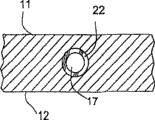
Fig. 1 shows the vertical view of abrasive sheet of the present invention.
Fig. 2 shows the side view of the abrasive sheet of being got along the line segment A-A of Fig. 1, and does not wherein include auxiliary pad.
Fig. 3 shows the zoomed-in view of the abrasive sheet of being got along the line segment B-B of Fig. 1, and it does not include auxiliary pad.
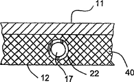
Fig. 4 shows the side view of the abrasive sheet of being got along the line segment A-A of Fig. 1, and comprising an auxiliary pad.
Fig. 5 shows the zoomed-in view of the abrasive sheet of being got along the line segment B-B of Fig. 1, and comprising an auxiliary pad.
Fig. 6 shows the side view of the abrasive sheet of being got along the line segment A-A of Fig. 1, and comprising a solid bed and an auxiliary pad.
The specific embodiment
The invention provides a kind of abrasive sheet and in order to grind the method for a substrate (especially semiconductor device).As shown in Figure 1, the main body of abrasive sheet 10 comprises a front 11, a back side 12 and peripheral surface 13.One lapped face be can't help the front just to be provided by the back side.Though the main body of abrasive sheet 10 can have any shape, yet it preferably forms one and has the circle of rotary middle spindle 14.One endpoint detection mouth 15 extends through the main body of this abrasive sheet, and is through to the back side 12 by positive 11.One discharging conduit 16 forms fluid with this endpoint detection mouth 15 and is communicated with.
In use, this abrasive sheet forms with substrate to be ground and contact, and this abrasive sheet and substrate are to be present under therebetween the situation at the grinding synthetic to move relative to each other.This endpoint detection mouth can monitor this milled processed in the original place, should too much grinding synthetic can be discharged by the detecting mouth by the discharging conduit simultaneously, because too much grinding synthetic can hamper the supervision of milled processed.In detail, when substrate to be ground and when mobile with respect to abrasive sheet, its part of this substrate by the detecting mouth of this abrasive sheet can expose out (as inspection with).Owing to check for substrate during grinding, so this milled processed can be with respect to this substrate and come abort process (that is, detect and grind end points) at reasonable time point.
The main body of abrasive sheet can comprise any suitable material or the composite structure of material.Best, the main body of this abrasive sheet comprises a polymeric material, such as polyurethane.Any suitable material all can be placed on the front and/or the back side of abrasive sheet, so that lapped face to be provided.For instance, this front can comprise the material that is different from this abrasive sheet main body, so that this front is more suitable for as the lapped face that grinds substrate to be ground with this abrasive sheet.
Discharging conduit 16 forms fluid with endpoint detection mouth 15 and is communicated with, shown in Fig. 1 and 2.This discharging conduit can suitably be connected perforation 15 with the opening 17 that is arranged in peripheral surface.This opening 17 can have any suitable shape or size.Discharging conduit 16 can be at any position between perforation 15 and the opening in peripheral surface 17.It can expose to the front 11 or the back side 12 of abrasive sheet, or is embedded in the main body 10 of abrasive sheet.When the discharging conduit exposed to the front of abrasive sheet or the back side, this discharging conduit just formed a chase in the surface of abrasive sheet.Best, this discharging conduit 16 (for example, on its whole length) is by 23,24 coverings of a part at the front and the back side of abrasive sheet.This discharging conduit can be made of single conduit or a plurality of conduit, and these a plurality of conduits can be identical or different on structure and profile.The thickness of this discharging conduit is the 10-90% of the thickness of this abrasive sheet substantially.This discharging conduit itself can be the part (that is, partially or even wholly be formed on the conduit in the abrasive sheet) of this abrasive sheet, and perhaps this discharging conduit can be the separate type assembly that any suitable material constitutes.This discharging conduit can have any suitable moulding, for example a body 22.In the abrasive sheet that a kind of its discharging conduit is made of a separate type body, this body is preferably made by polymeric material, and has any suitable width and cross sectional shape (for example, circle 22 as shown in Figure 3, or rectangle).The discharging conduit of abrasive sheet can have any suitable compressibility, but preferably its degree of compressibility is about as much as the compressibility of the material that constitutes this abrasive sheet main body.
This abrasive sheet also can comprise an auxiliary pad 40, shown in Fig. 4 and 5.Should can be constituted by any suitable material by auxiliary pad, but preferably made by a kind of material that can not absorb the grinding synthetic.Should can have any suitable thickness by auxiliary pad, and can with any part on the surface of abrasive sheet, perhaps, extend jointly, and have a suitable gap portions that aligns with this endpoint detection mouth with the whole surface of abrasive sheet.Should auxiliary pad preferably be positioned in contrast to desire with contacted another surface of this substrate to be ground upward (that is, in contrast to lapped face), and it desires abrasive sheet to be supported on the contacted surface of supporting construction on the lapping device with the pressure head of this lapping device or other preferably to constitute this abrasive sheet.When abrasive sheet comprised an auxiliary pad, this discharging conduit preferably was positioned in the auxiliary pad.In order to increase the local robustness of detecting mouth, a solid bed 60 can be used with this abrasive sheet.This solid bed can be made of any suitable material, and when being used with an abrasive sheet that includes auxiliary pad, it is preferably disposed between other position of this auxiliary pad and abrasive sheet, as shown in Figure 6.Best, this solid bed is made of polymeric material, such as polynary carbonate.This solid bed can have any suitable thickness, to have suitable flintiness.This solid bed can only make an addition to the zone that surrounds this discharging conduit, or forms a layer body that extends jointly with some or all zone at all the other positions of whole abrasive sheet, and has one and the suitable gap portions that aligns of endpoint detection mouth.
The present invention also comprises a kind of method of making this abrasive sheet.This method comprises that (a) provides a main body, it has a front, a back side and a peripheral surface, (b) on main body, provide a lapped face, (c) formation one is through to the perforation at the back side by the front, with as an endpoint detection mouth, and (d) in main body, form a discharging conduit, and form fluid and be communicated with this perforation, to form an abrasive sheet by this main body, this abrasive sheet comprises lapped face, endpoint detection mouth and discharging conduit by this.In above-mentioned project, for example, main body, lapped face, abrasive sheet and discharging conduit are to disclose all hereinbefore.
The present invention also provides a kind of method of grinding one substrate, it comprises use abrasive sheet of the present invention, for example, contacts with the surface of this substrate by making this abrasive sheet, and grind under the situation of synthetic existence one, this abrasive sheet is moved with respect to substrate surface.Best, the polishing progress of this substrate can see through this endpoint detection mouth and be monitored by any suitable technology.Be different from and be collected in this endpoint detection mouth, this flows into certain part at least of the grinding synthetic of endpoint detection mouth, and preferably all or whole in fact grinding synthetics, can flow into via the discharging conduit in the suitable opening in the peripheral surface.Best, this grinding pad is to rotate continuously during grinding, and makes this flow into the grinding synthetic in the endpoint detection mouth, can be by centrifugal force and capillary auxiliary and got rid of via this discharging conduit.Grind synthetic this discharging conduit that preferably keeps flowing through,, can guarantee that this endpoint detection mouth is unimpeded, and can accurately monitor the polishing progress of substrate to be ground with during milled processed.Generally speaking, the grinding synthetic that flows into this endpoint detection mouth and discharging conduit concentrates in the opening of peripheral surface, and is preferably in and leaves this discharging conduit and just collected afterwards.The grinding synthetic of being concentrated at least some, and can in milled processed, recycle use for whole or essence is whole.
The present invention grinds the method for a substrate can or polish any substrate in order to grinding, for example, and by the substrate that glass, metal, metal oxide, metal composite, semiconductor substrate or its combined material constituted.This substrate can comprise, comprise substantially or comprise any proper metal.For instance, proper metal comprises copper, aluminium, tantalum, titanium, tungsten, gold, platinum, iridium, ruthenium and synthetic thereof (for example alloy or mixture).This substrate can comprise, comprise substantially or comprise any proper metal oxide.For instance, the proper metal oxide comprises aluminium oxide, silica, titanium oxide, cerium oxide, zirconium dioxide, germanium oxide, magnesia and composition thereof.In addition, this substrate can comprise, comprise substantially or comprise any proper metal synthetic.For instance, the proper metal synthetic comprises that metal nitride (for example, tantalum nitride, titanium nitride, and tungsten nitride), metal carbides (for example, carborundum and tungsten carbide), nickel-phosphorus, aluminium-silicon boron, silicon boron glass, silicon phosphorus glass (PSG), silicon phosphorus boron glass (BPSG), silicon/germanium alloy and silicon/germanium/carbon alloy.This substrate can comprise, comprise substantially or comprise any suitable semiconductor substrate.Suitable semiconductor substrate comprises silicon (silicon-on-insulator) and GaAs on monocrystalline silicon, polysilicon, no silicon metal, the insulant.
Method of the present invention can be used in polishing or grind many hard workpiece, such as internal memory or hard disk, metal (for example, noble metal), primary insulation (ILD) layer, micro-electromechanical system, ferroelectric, magnetic head, polymeric membrane and have film low and high-k.Be meant any disk, hard disk or preserve the internal memory disc of information with the dish-like formula of electricity at this used " internal memory or hard disk ".Internal memory or hard disk have one usually and comprise the surface of nickel-phosphorus, but should also can comprise any other suitable material in the surface.
Method of the present invention is to be specially adapted to grind or polishing semiconductor device, for example, has the semiconductor device of how much of the device characteristics of about 0.25 micron or littler (for example, 0.18 micron or littler).At this used " device characteristic " speech, be meant the simple function assembly, such as transistor, resistor, capacitor, integrated circuit or the like.Method of the present invention can be in order to grind or the surface of polishing semiconductor device, for example during semiconductor is made by the formed isolation structure of shallow trench partition method (STI grinding).The inventive method can also a kind of primary insulation (ILD grinding) structure grind the dielectric or the metal level of semiconductor device.
The method that the present invention grinds a substrate also can comprise makes a light (for example, a laser) arrive the surface of substrate by the endpoint detection mouth of abrasive sheet, for example during grinding or polishing a substrate, to check or to monitor this milled processed situation.In order to check and to monitor the technology of milled processed, can reach by light or other ray that substrate surface reflected by analyzing, this type of technology is that industry is known.For instance, these class methods are to disclose at United States Patent (USP) the 5th, 196 No. 353,5,433, No. 651,5,609, No. 511,5,643, No. 046,5,658, No. 183,5,730, No. 642,5,838, No. 447,5,872, No. 633,5,893, No. 796,5,949, No. 927 and 5,964, No. 643.Owing in the endpoint detection mouth of abrasive sheet of the present invention, do not use stopper, the challenge that the stopper optics flaw of therefore just can preventing is caused.This endpoint detection mouth also can be used with any other technology, to check or to monitor this milled processed situation.Best, at the inspection and the supervision of the milled processed process of substrate to be ground, it just can determine the grinding end points, that is at a specific substrate, it can determine when finish this polish process.
Here cite all documents, comprise patent, patent specification, and open source literature, all be incorporated in full in this specification, with as a reference with it for reference.
Though the present invention focuses on a preferred embodiment and illustrates as above, yet for those skilled in the art as can be seen, the preferred embodiments of the present invention still can have many variations, and the present invention also can implement in the mode that is different from above detailed description.Therefore, in the spirit and category of claims of the present invention, the present invention still comprises all this type of modification and variation.
Claims (19)
1. abrasive sheet, it comprises
(a) main body, it comprises a front, a back side and a peripheral surface, described peripheral surface comprises an opening,
(b) lapped face is arranged at the front or the back side of described main body,
(c) an endpoint detection mouth, its front by main body is through to the back side, and
(d) a discharging conduit, it is communicated with the opening formation fluid of this endpoint detection mouth and described peripheral surface,
It is characterized in that described main body comprises a polymeric material.
2. according to the abrasive sheet of claim 1, wherein this discharging conduit exposes to the front.
3. according to the abrasive sheet of claim 1, wherein this discharging conduit is covered by a position in front.
4. according to the abrasive sheet of claim 3, wherein this discharging conduit is covered by a position at the back side.
5. according to the abrasive sheet of claim 4, wherein this abrasive sheet also comprises a body, and it constitutes this discharging conduit.
6. according to the abrasive sheet of claim 5, wherein this body is made of polymeric material.
7. according to the abrasive sheet of claim 1, wherein this lapped face is by placing the front of main body or the back side to form a material.
8. according to the abrasive sheet of claim 1, wherein this polymeric material comprises polyurethane.
9. according to the abrasive sheet of claim 1, wherein this letdown tank road has a compressibility, and it approximately is equal to the compressibility of this polymeric material.
10. according to the abrasive sheet of claim 1, wherein also comprise an auxiliary pad.
11. according to the abrasive sheet of claim 10, wherein said discharging conduit is positioned at described auxiliary pad.
12., wherein also comprise a solid bed according to the abrasive sheet of claim 10.
13. a method of making each described abrasive sheet of claim 1-9, it comprises
(a) provide a main body, it has a front, a back side and a peripheral surface, and described main body comprises a polymeric material, and described peripheral surface comprises an opening,
(b) on main body, provide a lapped face,
(c) form one and be through to the perforation at the back side by the front, with as an endpoint detection mouth, and
(d) in main body, form a discharging conduit, and be communicated with the opening formation fluid of this perforation and described peripheral surface,
To form an abrasive sheet by this main body, this abrasive sheet comprises lapped face, endpoint detection mouth and discharging conduit by this.
14. a method of grinding a substrate, it comprises
(a) provide a kind of abrasive sheet as claimed in claim 1,
(b) provide a substrate,
(c) provide a polishing fluid to this lapped face or this substrate and this lapped face,
(d) this lapped face is contacted with substrate, and
(e) this lapped face is moved with respect to substrate, to grind this substrate.
15. according to the method for claim 14, wherein during grinding, some polishing fluid flows into this endpoint detection mouth at least, and this discharging conduit of flowing through.
16., wherein, also comprise making light pass through this endpoint detection mouth, to monitor the polishing progress of this substrate according to the method for claim 15.
17. according to the method for claim 16, wherein this light is a laser.
18. according to the method for claim 16, wherein this milled processed program is according to deciding termination by the result who monitors this substrate grinding.
19., wherein, comprise that further at least a portion with polishing fluid is recycled to lapped face and/or this substrate by the discharging conduit according to the method for claim 15.
Applications Claiming Priority (2)
| Application Number | Priority Date | Filing Date | Title |
|---|---|---|---|
| US09/788,082 US6623331B2 (en) | 2001-02-16 | 2001-02-16 | Polishing disk with end-point detection port |
| US09/788,082 | 2001-02-16 |
Publications (2)
| Publication Number | Publication Date |
|---|---|
| CN1484568A CN1484568A (en) | 2004-03-24 |
| CN100503168C true CN100503168C (en) | 2009-06-24 |
Family
ID=25143403
Family Applications (1)
| Application Number | Title | Priority Date | Filing Date |
|---|---|---|---|
| CNB028034600A Expired - Fee Related CN100503168C (en) | 2001-02-16 | 2002-02-05 | Polishing disk with end-point detection port |
Country Status (8)
| Country | Link |
|---|---|
| US (1) | US6623331B2 (en) |
| EP (1) | EP1368157B1 (en) |
| JP (1) | JP4369122B2 (en) |
| CN (1) | CN100503168C (en) |
| AU (1) | AU2002306506A1 (en) |
| DE (1) | DE60201515T2 (en) |
| TW (1) | TWI222389B (en) |
| WO (1) | WO2002064315A1 (en) |
Cited By (1)
| Publication number | Priority date | Publication date | Assignee | Title |
|---|---|---|---|---|
| CN102133734B (en) * | 2010-01-21 | 2015-02-04 | 智胜科技股份有限公司 | Grinding pad with detecting window and manufacturing method thereof |
Families Citing this family (23)
| Publication number | Priority date | Publication date | Assignee | Title |
|---|---|---|---|---|
| US8485862B2 (en) | 2000-05-19 | 2013-07-16 | Applied Materials, Inc. | Polishing pad for endpoint detection and related methods |
| US6599765B1 (en) * | 2001-12-12 | 2003-07-29 | Lam Research Corporation | Apparatus and method for providing a signal port in a polishing pad for optical endpoint detection |
| US7001242B2 (en) * | 2002-02-06 | 2006-02-21 | Applied Materials, Inc. | Method and apparatus of eddy current monitoring for chemical mechanical polishing |
| US6913514B2 (en) * | 2003-03-14 | 2005-07-05 | Ebara Technologies, Inc. | Chemical mechanical polishing endpoint detection system and method |
| US7354334B1 (en) * | 2004-05-07 | 2008-04-08 | Applied Materials, Inc. | Reducing polishing pad deformation |
| US7018581B2 (en) | 2004-06-10 | 2006-03-28 | Rohm And Haas Electronic Materials Cmp Holdings, Inc. | Method of forming a polishing pad with reduced stress window |
| US7252871B2 (en) * | 2004-06-16 | 2007-08-07 | Rohm And Haas Electronic Materials Cmp Holdings, Inc. | Polishing pad having a pressure relief channel |
| US20060286906A1 (en) * | 2005-06-21 | 2006-12-21 | Cabot Microelectronics Corporation | Polishing pad comprising magnetically sensitive particles and method for the use thereof |
| US20060291530A1 (en) * | 2005-06-23 | 2006-12-28 | Alexander Tregub | Treatment of CMP pad window to improve transmittance |
| US20070037487A1 (en) * | 2005-08-10 | 2007-02-15 | Kuo Charles C | Polishing pad having a sealed pressure relief channel |
| TWI287486B (en) * | 2006-05-04 | 2007-10-01 | Iv Technologies Co Ltd | Polishing pad and method thereof |
| US7998866B2 (en) * | 2006-09-05 | 2011-08-16 | Cabot Microelectronics Corporation | Silicon carbide polishing method utilizing water-soluble oxidizers |
| US7678700B2 (en) * | 2006-09-05 | 2010-03-16 | Cabot Microelectronics Corporation | Silicon carbide polishing method utilizing water-soluble oxidizers |
| US7455571B1 (en) | 2007-06-20 | 2008-11-25 | Rohm And Haas Electronic Materials Cmp Holdings, Inc. | Window polishing pad |
| US9017140B2 (en) | 2010-01-13 | 2015-04-28 | Nexplanar Corporation | CMP pad with local area transparency |
| US9156124B2 (en) | 2010-07-08 | 2015-10-13 | Nexplanar Corporation | Soft polishing pad for polishing a semiconductor substrate |
| CN102441839B (en) * | 2011-11-11 | 2014-06-04 | 上海华力微电子有限公司 | Method for improving CMP (chemical mechanical polishing) process stability of polishing materials on polishing pad |
| US20140120802A1 (en) * | 2012-10-31 | 2014-05-01 | Wayne O. Duescher | Abrasive platen wafer surface optical monitoring system |
| TWI518176B (en) * | 2015-01-12 | 2016-01-21 | 三芳化學工業股份有限公司 | Polishing pad and method for making the same |
| US9475168B2 (en) | 2015-03-26 | 2016-10-25 | Rohm And Haas Electronic Materials Cmp Holdings, Inc. | Polishing pad window |
| US10569383B2 (en) * | 2017-09-15 | 2020-02-25 | Rohm And Haas Electronic Materials Cmp Holdings, Inc. | Flanged optical endpoint detection windows and CMP polishing pads containing them |
| JP7083722B2 (en) * | 2018-08-06 | 2022-06-13 | 株式会社荏原製作所 | Polishing equipment and polishing method |
| JP7162465B2 (en) | 2018-08-06 | 2022-10-28 | 株式会社荏原製作所 | Polishing device and polishing method |
Citations (4)
| Publication number | Priority date | Publication date | Assignee | Title |
|---|---|---|---|---|
| US6014218A (en) * | 1997-12-03 | 2000-01-11 | Siemens Aktiengesellschaft | Device and method for end-point monitoring used in the polishing of components, in particular semiconductor components |
| US6095902A (en) * | 1998-09-23 | 2000-08-01 | Rodel Holdings, Inc. | Polyether-polyester polyurethane polishing pads and related methods |
| US6106728A (en) * | 1997-06-23 | 2000-08-22 | Iida; Shinya | Slurry recycling system and method for CMP apparatus |
| US6142857A (en) * | 1998-01-06 | 2000-11-07 | Speedfam-Ipec Corporation | Wafer polishing with improved backing arrangement |
Family Cites Families (55)
| Publication number | Priority date | Publication date | Assignee | Title |
|---|---|---|---|---|
| US4317698A (en) | 1980-11-13 | 1982-03-02 | Applied Process Technology, Inc. | End point detection in etching wafers and the like |
| DE3132028A1 (en) | 1981-08-13 | 1983-03-03 | Roehm Gmbh | IMPROVED POLISHING PLATES FOR POLISHING PLASTIC SURFACES |
| US4462860A (en) | 1982-05-24 | 1984-07-31 | At&T Bell Laboratories | End point detection |
| US4611919A (en) | 1984-03-09 | 1986-09-16 | Tegal Corporation | Process monitor and method thereof |
| JPS60242975A (en) | 1984-05-14 | 1985-12-02 | Kanebo Ltd | Surface grinding device |
| US4660979A (en) | 1984-08-17 | 1987-04-28 | At&T Technologies, Inc. | Method and apparatus for automatically measuring semiconductor etching process parameters |
| US4674236A (en) | 1985-05-13 | 1987-06-23 | Toshiba Machine Co., Ltd. | Polishing machine and method of attaching emery cloth to the polishing machine |
| JPS63147327A (en) | 1986-12-10 | 1988-06-20 | Dainippon Screen Mfg Co Ltd | Detection of end point during surface treatment |
| US4851311A (en) | 1987-12-17 | 1989-07-25 | Texas Instruments Incorporated | Process for determining photoresist develop time by optical transmission |
| US4826563A (en) | 1988-04-14 | 1989-05-02 | Honeywell Inc. | Chemical polishing process and apparatus |
| JPH0252205A (en) | 1988-08-17 | 1990-02-21 | Dainippon Screen Mfg Co Ltd | Film thickness measuring method |
| JPH02137852A (en) | 1988-11-18 | 1990-05-28 | Dainippon Screen Mfg Co Ltd | Development end point detecting method for photoresist |
| US5229303A (en) | 1989-08-29 | 1993-07-20 | At&T Bell Laboratories | Device processing involving an optical interferometric thermometry using the change in refractive index to measure semiconductor wafer temperature |
| US5166080A (en) | 1991-04-29 | 1992-11-24 | Luxtron Corporation | Techniques for measuring the thickness of a film formed on a substrate |
| US5076024A (en) | 1990-08-24 | 1991-12-31 | Intelmatec Corporation | Disk polisher assembly |
| US5270222A (en) | 1990-12-31 | 1993-12-14 | Texas Instruments Incorporated | Method and apparatus for semiconductor device fabrication diagnosis and prognosis |
| US5189490A (en) | 1991-09-27 | 1993-02-23 | University Of Hartford | Method and apparatus for surface roughness measurement using laser diffraction pattern |
| US5499733A (en) | 1992-09-17 | 1996-03-19 | Luxtron Corporation | Optical techniques of measuring endpoint during the processing of material layers in an optically hostile environment |
| US5733171A (en) | 1996-07-18 | 1998-03-31 | Speedfam Corporation | Apparatus for the in-process detection of workpieces in a CMP environment |
| US5433650A (en) | 1993-05-03 | 1995-07-18 | Motorola, Inc. | Method for polishing a substrate |
| JP3326443B2 (en) | 1993-08-10 | 2002-09-24 | 株式会社ニコン | Wafer polishing method and apparatus therefor |
| US5891352A (en) | 1993-09-16 | 1999-04-06 | Luxtron Corporation | Optical techniques of measuring endpoint during the processing of material layers in an optically hostile environment |
| US5441598A (en) | 1993-12-16 | 1995-08-15 | Motorola, Inc. | Polishing pad for chemical-mechanical polishing of a semiconductor substrate |
| US5433651A (en) | 1993-12-22 | 1995-07-18 | International Business Machines Corporation | In-situ endpoint detection and process monitoring method and apparatus for chemical-mechanical polishing |
| US5413941A (en) | 1994-01-06 | 1995-05-09 | Micron Technology, Inc. | Optical end point detection methods in semiconductor planarizing polishing processes |
| JPH08316279A (en) | 1995-02-14 | 1996-11-29 | Internatl Business Mach Corp <Ibm> | Thickness measuring method for semiconductor base body and its measurement device |
| US5893796A (en) | 1995-03-28 | 1999-04-13 | Applied Materials, Inc. | Forming a transparent window in a polishing pad for a chemical mechanical polishing apparatus |
| US5533923A (en) | 1995-04-10 | 1996-07-09 | Applied Materials, Inc. | Chemical-mechanical polishing pad providing polishing unformity |
| IL113829A (en) | 1995-05-23 | 2000-12-06 | Nova Measuring Instr Ltd | Apparatus for optical inspection of wafers during polishing |
| JP3042593B2 (en) * | 1995-10-25 | 2000-05-15 | 日本電気株式会社 | Polishing pad |
| US5695601A (en) | 1995-12-27 | 1997-12-09 | Kabushiki Kaisha Toshiba | Method for planarizing a semiconductor body by CMP method and an apparatus for manufacturing a semiconductor device using the method |
| US5681216A (en) | 1996-02-06 | 1997-10-28 | Elantec, Inc. | High precision polishing tool |
| US6074287A (en) | 1996-04-12 | 2000-06-13 | Nikon Corporation | Semiconductor wafer polishing apparatus |
| US5800248A (en) | 1996-04-26 | 1998-09-01 | Ontrak Systems Inc. | Control of chemical-mechanical polishing rate across a substrate surface |
| US5663797A (en) | 1996-05-16 | 1997-09-02 | Micron Technology, Inc. | Method and apparatus for detecting the endpoint in chemical-mechanical polishing of semiconductor wafers |
| US5910846A (en) | 1996-05-16 | 1999-06-08 | Micron Technology, Inc. | Method and apparatus for detecting the endpoint in chemical-mechanical polishing of semiconductor wafers |
| JP2865061B2 (en) | 1996-06-27 | 1999-03-08 | 日本電気株式会社 | Polishing pad, polishing apparatus, and semiconductor device manufacturing method |
| US5645469A (en) | 1996-09-06 | 1997-07-08 | Advanced Micro Devices, Inc. | Polishing pad with radially extending tapered channels |
| US5795218A (en) | 1996-09-30 | 1998-08-18 | Micron Technology, Inc. | Polishing pad with elongated microcolumns |
| US5674116A (en) | 1996-10-09 | 1997-10-07 | Cmi International Inc. | Disc with coolant passages for an abrasive machining assembly |
| US6246098B1 (en) | 1996-12-31 | 2001-06-12 | Intel Corporation | Apparatus for reducing reflections off the surface of a semiconductor surface |
| US5838448A (en) | 1997-03-11 | 1998-11-17 | Nikon Corporation | CMP variable angle in situ sensor |
| US6102775A (en) | 1997-04-18 | 2000-08-15 | Nikon Corporation | Film inspection method |
| DE19720623C1 (en) | 1997-05-16 | 1998-11-05 | Siemens Ag | Polishing device for semiconductor substrate |
| US6108091A (en) | 1997-05-28 | 2000-08-22 | Lam Research Corporation | Method and apparatus for in-situ monitoring of thickness during chemical-mechanical polishing |
| US6146248A (en) * | 1997-05-28 | 2000-11-14 | Lam Research Corporation | Method and apparatus for in-situ end-point detection and optimization of a chemical-mechanical polishing process using a linear polisher |
| US5882251A (en) | 1997-08-19 | 1999-03-16 | Lsi Logic Corporation | Chemical mechanical polishing pad slurry distribution grooves |
| US5963781A (en) | 1997-09-30 | 1999-10-05 | Intel Corporation | Technique for determining semiconductor substrate thickness |
| US5972162A (en) | 1998-01-06 | 1999-10-26 | Speedfam Corporation | Wafer polishing with improved end point detection |
| JPH11254298A (en) * | 1998-03-06 | 1999-09-21 | Speedfam Co Ltd | Slurry circulation supplying type surface polishing device |
| US6068539A (en) | 1998-03-10 | 2000-05-30 | Lam Research Corporation | Wafer polishing device with movable window |
| US6106662A (en) * | 1998-06-08 | 2000-08-22 | Speedfam-Ipec Corporation | Method and apparatus for endpoint detection for chemical mechanical polishing |
| US6146242A (en) * | 1999-06-11 | 2000-11-14 | Strasbaugh, Inc. | Optical view port for chemical mechanical planarization endpoint detection |
| US6077147A (en) | 1999-06-19 | 2000-06-20 | United Microelectronics Corporation | Chemical-mechanical polishing station with end-point monitoring device |
| JP3508747B2 (en) | 2001-08-08 | 2004-03-22 | 株式会社ニコン | Polishing pad and wafer polishing apparatus |
-
2001
- 2001-02-16 US US09/788,082 patent/US6623331B2/en not_active Expired - Lifetime
- 2001-12-31 TW TW090133214A patent/TWI222389B/en not_active IP Right Cessation
-
2002
- 2002-02-05 WO PCT/US2002/004587 patent/WO2002064315A1/en active IP Right Grant
- 2002-02-05 DE DE60201515T patent/DE60201515T2/en not_active Expired - Lifetime
- 2002-02-05 AU AU2002306506A patent/AU2002306506A1/en not_active Abandoned
- 2002-02-05 CN CNB028034600A patent/CN100503168C/en not_active Expired - Fee Related
- 2002-02-05 EP EP02740116A patent/EP1368157B1/en not_active Expired - Lifetime
- 2002-02-05 JP JP2002564089A patent/JP4369122B2/en not_active Expired - Fee Related
Patent Citations (4)
| Publication number | Priority date | Publication date | Assignee | Title |
|---|---|---|---|---|
| US6106728A (en) * | 1997-06-23 | 2000-08-22 | Iida; Shinya | Slurry recycling system and method for CMP apparatus |
| US6014218A (en) * | 1997-12-03 | 2000-01-11 | Siemens Aktiengesellschaft | Device and method for end-point monitoring used in the polishing of components, in particular semiconductor components |
| US6142857A (en) * | 1998-01-06 | 2000-11-07 | Speedfam-Ipec Corporation | Wafer polishing with improved backing arrangement |
| US6095902A (en) * | 1998-09-23 | 2000-08-01 | Rodel Holdings, Inc. | Polyether-polyester polyurethane polishing pads and related methods |
Cited By (1)
| Publication number | Priority date | Publication date | Assignee | Title |
|---|---|---|---|---|
| CN102133734B (en) * | 2010-01-21 | 2015-02-04 | 智胜科技股份有限公司 | Grinding pad with detecting window and manufacturing method thereof |
Also Published As
| Publication number | Publication date |
|---|---|
| US20020115379A1 (en) | 2002-08-22 |
| WO2002064315A1 (en) | 2002-08-22 |
| EP1368157B1 (en) | 2004-10-06 |
| DE60201515T2 (en) | 2005-02-03 |
| EP1368157A1 (en) | 2003-12-10 |
| JP4369122B2 (en) | 2009-11-18 |
| WO2002064315A8 (en) | 2004-04-08 |
| JP2004522598A (en) | 2004-07-29 |
| US6623331B2 (en) | 2003-09-23 |
| TWI222389B (en) | 2004-10-21 |
| AU2002306506A1 (en) | 2002-08-28 |
| CN1484568A (en) | 2004-03-24 |
| DE60201515D1 (en) | 2004-11-11 |
Similar Documents
| Publication | Publication Date | Title |
|---|---|---|
| CN100503168C (en) | Polishing disk with end-point detection port | |
| US7189141B2 (en) | Polishing pad with transparent window having reduced window leakage for a chemical mechanical polishing apparatus | |
| JP6030703B2 (en) | Use of CsOH in dielectric CMP slurry | |
| US6723144B2 (en) | Semiconductor device fabricating method | |
| KR101195276B1 (en) | Polishing pad comprising hydrophobic region and endpoint detection port | |
| TW548734B (en) | Optical window structure | |
| TWI535524B (en) | Grinding method of grinding and polishing pad | |
| TW542768B (en) | Device and method for polishing a semiconductor substrate | |
| JP2002530861A (en) | Method for reducing dishing speed during CMP in metal semiconductor structure | |
| TWI246722B (en) | Semiconductor substrate, method for fabricating the same, and method for fabricating semiconductor device | |
| US9539696B2 (en) | Retainer ring, polish apparatus, and polish method | |
| US6213852B1 (en) | Polishing apparatus and method of manufacturing a semiconductor device using the same | |
| US6312321B1 (en) | Polishing apparatus | |
| US6391779B1 (en) | Planarization process | |
| CN100464394C (en) | Manufacture of semiconductor device with cmp | |
| JP2004502311A (en) | Projection type gimbal point drive | |
| JP2000091415A (en) | Sti-forming method | |
| JP2009224680A (en) | Retainer ring, and manufacturing method of semiconductor device | |
| CN112086354B (en) | Flattening method of IGBT device | |
| JP3823308B2 (en) | Semiconductor device polishing apparatus and polishing pad | |
| Kim et al. | Tribological approaches to material removal rate during chemical mechanical polishing | |
| TW525257B (en) | Improvement method of forming integrated circuit shallow trench isolation region | |
| US20220102285A1 (en) | Cmp safe alignment mark | |
| CN115056137A (en) | Polishing pad with grinding consistency end point detection window and application thereof | |
| KR19990008774A (en) | How to automatically detect the end point of chemical mechanical polishing using pH sensor |
Legal Events
| Date | Code | Title | Description |
|---|---|---|---|
| C06 | Publication | ||
| PB01 | Publication | ||
| C10 | Entry into substantive examination | ||
| SE01 | Entry into force of request for substantive examination | ||
| C14 | Grant of patent or utility model | ||
| GR01 | Patent grant | ||
| CF01 | Termination of patent right due to non-payment of annual fee | ||
| CF01 | Termination of patent right due to non-payment of annual fee |
Granted publication date: 20090624 Termination date: 20180105 |