CN100523887C - Electromagnetic wave frequency filter - Google Patents
Electromagnetic wave frequency filter Download PDFInfo
- Publication number
- CN100523887C CN100523887C CNB2004800321134A CN200480032113A CN100523887C CN 100523887 C CN100523887 C CN 100523887C CN B2004800321134 A CNB2004800321134 A CN B2004800321134A CN 200480032113 A CN200480032113 A CN 200480032113A CN 100523887 C CN100523887 C CN 100523887C
- Authority
- CN
- China
- Prior art keywords
- waveguide
- electromagnetic wave
- resonator
- output
- input waveguide
- Prior art date
- Legal status (The legal status is an assumption and is not a legal conclusion. Google has not performed a legal analysis and makes no representation as to the accuracy of the status listed.)
- Expired - Fee Related
Links
Images


Classifications
-
- G—PHYSICS
- G02—OPTICS
- G02B—OPTICAL ELEMENTS, SYSTEMS OR APPARATUS
- G02B6/00—Light guides; Structural details of arrangements comprising light guides and other optical elements, e.g. couplings
- G02B6/10—Light guides; Structural details of arrangements comprising light guides and other optical elements, e.g. couplings of the optical waveguide type
- G02B6/12—Light guides; Structural details of arrangements comprising light guides and other optical elements, e.g. couplings of the optical waveguide type of the integrated circuit kind
- G02B6/12007—Light guides; Structural details of arrangements comprising light guides and other optical elements, e.g. couplings of the optical waveguide type of the integrated circuit kind forming wavelength selective elements, e.g. multiplexer, demultiplexer
-
- G—PHYSICS
- G02—OPTICS
- G02B—OPTICAL ELEMENTS, SYSTEMS OR APPARATUS
- G02B6/00—Light guides; Structural details of arrangements comprising light guides and other optical elements, e.g. couplings
- G02B6/10—Light guides; Structural details of arrangements comprising light guides and other optical elements, e.g. couplings of the optical waveguide type
- G02B6/12—Light guides; Structural details of arrangements comprising light guides and other optical elements, e.g. couplings of the optical waveguide type of the integrated circuit kind
-
- B—PERFORMING OPERATIONS; TRANSPORTING
- B82—NANOTECHNOLOGY
- B82Y—SPECIFIC USES OR APPLICATIONS OF NANOSTRUCTURES; MEASUREMENT OR ANALYSIS OF NANOSTRUCTURES; MANUFACTURE OR TREATMENT OF NANOSTRUCTURES
- B82Y20/00—Nanooptics, e.g. quantum optics or photonic crystals
-
- G—PHYSICS
- G02—OPTICS
- G02B—OPTICAL ELEMENTS, SYSTEMS OR APPARATUS
- G02B6/00—Light guides; Structural details of arrangements comprising light guides and other optical elements, e.g. couplings
- G02B6/10—Light guides; Structural details of arrangements comprising light guides and other optical elements, e.g. couplings of the optical waveguide type
- G02B6/12—Light guides; Structural details of arrangements comprising light guides and other optical elements, e.g. couplings of the optical waveguide type of the integrated circuit kind
- G02B6/122—Basic optical elements, e.g. light-guiding paths
- G02B6/1225—Basic optical elements, e.g. light-guiding paths comprising photonic band-gap structures or photonic lattices
-
- H—ELECTRICITY
- H01—ELECTRIC ELEMENTS
- H01P—WAVEGUIDES; RESONATORS, LINES, OR OTHER DEVICES OF THE WAVEGUIDE TYPE
- H01P1/00—Auxiliary devices
- H01P1/20—Frequency-selective devices, e.g. filters
- H01P1/2005—Electromagnetic photonic bandgaps [EPB], or photonic bandgaps [PBG]
-
- G—PHYSICS
- G02—OPTICS
- G02B—OPTICAL ELEMENTS, SYSTEMS OR APPARATUS
- G02B6/00—Light guides; Structural details of arrangements comprising light guides and other optical elements, e.g. couplings
- G02B6/10—Light guides; Structural details of arrangements comprising light guides and other optical elements, e.g. couplings of the optical waveguide type
- G02B6/12—Light guides; Structural details of arrangements comprising light guides and other optical elements, e.g. couplings of the optical waveguide type of the integrated circuit kind
- G02B2006/12133—Functions
- G02B2006/12164—Multiplexing; Demultiplexing
Abstract
In this electromagnetic wave frequency filter, an electromagnetic wave of a predetermined frequency matching a resonant frequency of a resonator 4 1 is transmitted from an input waveguide 2 to an output waveguide 3 through the resonator 4 1, and is outputted from a drop port P3 1. This filter has an input-waveguide-side reflector 21 1 and an output-waveguide-side reflector 31 1, which reflect the electromagnetic wave of the predetermined frequency. The electromagnetic wave frequency filter satisfies the following relation: Q(inb)/(1-costheta1)<<QV, Q(inb)/(1-costheta2)=Q(inr)/(1-costheta2), theta1, theta2 are not equal to 2Npi(N=0, 1,...), where 1 is a phase shift amount of the electromagnetic wave reflected by the input-waveguide-side reflector 21 1, 2 is a phase shift amount of the electromagnetic wave reflected by the output-waveguide-side reflector 31 1, Q inb is a Q-factor between the resonator 4 1 and the input waveguide 2, Q inr is a Q-factor between the resonator 4 1 and the output waveguide 3 1, and Q v is a Q-factor between the resonator 4 1 and free space.
Description
Technical field
The present invention relates to a kind of electromagnetic wave frequency filter, it is used for optionally obtaining the electromagnetic wave of preset frequency.
Background technology
Recently, in order to increase transmittability, the optical communication system that uses wavelength-division multiplex is very popular in the optical communication field etc.In the optical communication system that uses wavelength-division multiplex, need Port Multiplier, demultiplexer and wavelength filter (frequency filter).Usually, use array waveguide grating (AWG) as demultiplexer.Yet because array waveguide grating is by using the silica-based optical waveguide to form so for about several square centimeters, looking forward to that littler demultiplexer is arranged.Thereby, in order to make the demultiplexer miniaturization, go out to use the frequency filter of photonic crystal of the refractive index cycle structure of magnitude (in most of the cases, it is about the half-wavelength of estimating electromagnetic wave band) at many local developments with optical wavelength.
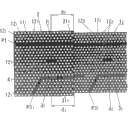
For example, as such frequency filter, the electromagnetic wave frequency filter as shown in 14A and 14B has been proposed.This electromagnetic wave frequency filter is in so-called template photon crystal 1, it is set on the Width of input waveguide 2 and 2 one-tenth spaced relationship of input waveguide to have linear input waveguide 2, output waveguide 3, and resonator 4 its be arranged between the center section of the center section of input waveguide 2 and output waveguide 3.In the electromagnetic wave frequency filter shown in Figure 14 A and the 14B, the formation of input waveguide 2 and output waveguide 3 is by make two linear defectives (that is the upset of refractive index periodic structure) in the refractive index cycle structure of the photon crystal 1 of two dimension.And the formation of resonator 4 is by make a point-like defective in the refractive index cycle structure at the photon crystal 1 of two dimension.In template 2 D photon crystal 1, the both sides on the thickness direction of plate 11 by high refractive index medium for example Si make, and with uniform low refractive index dielectric for example air and SiO
2In the middle of sandwiching, so electromagnetic wave (for example light) is limited by total reflection on thickness direction by restriction of the photon band gap in the plane and electromagnetic wave.
In the electromagnetic wave frequency filter of mentioning in the above, an end of input waveguide 2 is defined as port P1 (input end P1), and the other end of input waveguide 2 is defined as P2, and an end of output waveguide 3 is defined as port P3 (output terminal P3), and its other end is defined as port P4.When the electromagnetic wave of a plurality of different frequencies incided input end P1, from these a plurality of electromagnetic waves, the electromagnetic wave of the preset frequency of the resonance frequency of coupling resonator 4 was transferred to output waveguide 3 by resonator 4, is exported from output terminal P3 then.Electromagnetic wave with frequency different with the resonance frequency of resonator 4 is propagated towards the end 2 of input waveguide 2.In Figure 14 A, solid arrow illustrates the electromagnetic transmission path that has with the resonance frequency matched frequency of resonator 4, and alternately the length dash-dot arrows illustrates the frequency electromagnetic wave propagation path different with the resonance frequency of resonator 4.
Electromagnetic wave frequency filter above-mentioned can be used as photoswitch, and it changes the output of output terminal P3 and switches choosing from the electromagnetic of output terminal P3.
By the way, by using mode coupling theory, the present inventor is evaluated at output intensity from each port P1 to P4 and the output intensity from resonator 4 to free space in the conventional electromagnetic wave frequency filter shown in Figure 14 A, the 14B, and its result who obtains is shown in Figure 15.When the application model coupled wave theory, the Q factor between resonator 4 and input waveguide 2 is defined as Q
InAnd the Q factor between resonator 4 and free space is defined as Q
vIn Figure 15, transverse axis is represented Q
In/ Q
v, and Z-axis is represented output intensity, and the output intensity of " X1 " expression end P2 in Figure 15, the output intensity of " X2 " expression end P1, P3 and P4, " X3 " represents the output intensity of free space.As shown in figure 15, in conventional electromagnetic wave frequency filter, in theory only be 25% to the maximal value (being the wavelength efficiency of selection) of the transfer efficiency of output terminal P3, therefore the too not enough problem of transfer efficiency is just arranged.In addition, Q
InBe with resonator-input waveguide system in from the bleed relevant value of amount of the energy to input waveguide 2 of resonator 4.In other words, Q
InBe to be illustrated in resonator-input waveguide system, resonator 4 can store a value of how many energy.Q
InBe defined as follows and state expression formula:
Q
in=ω
0×W/(-dW/dt)
Wherein, ω
0The resonance frequency of expression resonator 4, W represents to be stored in the energy in the resonator 4, and (dW/dt) expression from resonator 4 to input waveguide the energy of time per unit loss 2.Q
vIt is relevant with the amount of the energy to free space that bleeds from resonator 4 in a resonator-free space system value.In other words, Q
vBe to be illustrated in resonator-free space system, resonator 4 can store a value of how many energy.Q
vBe defined as follows and state expression formula:
Q
v=ω
0×W/(-dW/dt)
Wherein, ω
0The resonance frequency of expression resonator 4, W represents to be stored in the energy in the resonator 4, and (the energy of time per unit loss dW/dt) representing from resonator 4 to free space.
In addition, proposed with the electromagnetic wave frequency filter shown in Figure 14 A and the 14B Comparatively speaking, can reach the electromagnetic wave frequency filter of higher transmission efficient.This electromagnetic wave frequency filter comprises 2 D photon crystal, wherein two dimensional surface is provided with the cylindrical bar of being made by the medium with refractive index higher than air, and input waveguide, output waveguide and two resonators (for example are formed on this 2 D photon crystal, see Japanese Kohyo (the translation version that country announces) No.2001-50887, p.22-23, p.40-46, Fig. 3,8 and 22, reach people " Couping of Modes Analysis ofResonant Channel Add-Drop Filters " such as C.Manolatou, IEEE JOURNAL QUANTUMELETRONICS, VOL 35, and NO 9,1999, p.1322-1331, reach people such as Shanhui Fan, " Channel Drop Tunneling through Localized States ", PHYSICAL REVIEWLETTERS, VOL 80, NO 5,1998, p.960-963).
In this electromagnetic wave frequency filter, electromagnetic wave of propagating towards the opposite end of the input end of input waveguide and the electromagnetic wave of propagating towards the opposite end of the output terminal of output waveguide can be by the mode of resonance cancellations of two resonators.Specifically, two resonators constitute the wherein symmetric pattern of two resonator in-phase oscillation and the antisymmetric mode of two resonator anti-phase oscillations, when the resonance frequency in symmetric pattern and the resonance frequency in antisymmetric mode are mutually the same, relative input waveguide in symmetric pattern, the rate of decay of output waveguide and out-of-plane free space its each all equals relative their rate of decay in antisymmetric mode respectively, phase differential between the vibration of the vibration of symmetric pattern and antisymmetric mode (for example satisfies specified conditions, π), electromagnetic wave of propagating from the reverse direction of the input end at input waveguide (upstream end) of resonator and the electromagnetic wave propagated from the reverse direction of the output terminal in output waveguide (output terminal) of resonator can be by cancellations.Therefore, can bring in from only specific output and optionally export electromagnetic wave.
Incidentally, in above-mentioned conventional electromagnetic wave frequency filter, can calculate each resonance frequency omega in symmetric pattern with following equation with two resonators
sWith the resonance frequency omega in antisymmetric mode
a:
ω
S=ω
O-{μ-(1/τe)×sinΦ-(1/τe’)×sinΦ’}
ω
a=ω
O+{μ-(1/τe)×sinΦ-(1/τe’)×sinΦ’}
Wherein μ is the binding energy by any waveguide not between resonator, Φ is at the phase-shift phase of resonator between them when resonator intercouples by input waveguide, Φ ' is at the phase-shift phase of resonator between them when resonator intercouples by output waveguide, (1/ τ e) is the rate of decay of the energy from the resonator to the input waveguide, (1/ τ e) ' be the rate of decay of the energy from the resonator to the output waveguide, ω
OIt is the resonant frequency under the situation of each resonator individualism.From top equation, can know and see the resonance frequency omega of these patterns
S, ω
aSubstantially different each other, therefore, in order to make these resonance frequency omega of two patterns
S, ω
aConsistent each other, must satisfy following conditions:
μ-(1/τe)×sinΦ-(1/τe’)×sinΦ’=0
Yet,, need to adopt complicated structure for the condition above satisfying.For example, must be set at a value inequality, perhaps will be set at other rods and Comparatively speaking be a very little value near the radius of the rod of resonator near the refractive index of the rod of resonator with other excellent refractive indexes.Therefore, many design limit are arranged, and be difficult to design and make electromagnetic wave frequency filter.
Summary of the invention
Consider the problems referred to above, the purpose of this invention is to provide a kind of electromagnetic wave frequency filter, choose the electromagnetic wave of preset frequency from the output terminal of output waveguide in the electromagnetic wave of a plurality of frequencies that it can be from be input to input waveguide, and can form by easier design.
Electromagnetic wave frequency filter according to the present invention comprises and is configured to electromagnetic input waveguide that receives a plurality of frequencies in the end be input to input waveguide and the output waveguide that is arranged side by side with described input waveguide, and is arranged on the resonator between input waveguide and the output waveguide.This resonator has the electromagnetic wave of preset frequency of predetermined resonance frequency and resonance and this resonance frequency coupling so that electromagnetic wave is transferred to output waveguide from input waveguide, makes thus to send electromagnetic wave from the output terminal of an end of output waveguide.The invention is characterized in input waveguide have the input waveguide side reverberator its be used for reflecting this resonance frequency electromagnetic wave at the opposition side of the resonator of an end of input waveguide, output waveguide have the output waveguide side reverberator its be used for the electromagnetic wave of reflection preset frequency on the opposition side of an end of output waveguide, this electromagnetic wave frequency filter satisfies relation of plane down:
Q
inb/(1-cosθ
1)《Q
V
Q
inb/(1-cosθ
2)=Q
inr/(1-cosθ
2)
θ
1、θ
2≠2Nπ(N=0,1,...)
Wherein, θ
1Be to be transfused to waveguide side reflector reflection and to get back near the resonator electromagnetic phase-shift phase, θ
2Be to be output waveguide side reflector reflection and to get back near the resonator electromagnetic phase-shift phase, Q
InbBe the Q factor between resonator and input waveguide, Q
InrBe the Q factor between resonator and output waveguide, and Q
VBe the Q factor between resonator and free space, Q
InbBe in resonator-input waveguide system with bleed from resonator to a relevant value of amount of the energy of input waveguide.In other words, Q
InbBe meant and be illustrated in the value how many energy resonator in resonator-input waveguide system can store.Q
InbDefine as following expression formula:
Q
inb=ω
0×W/(-dW/dt)
Wherein, ω
0The resonance frequency of expression resonator, W represents to be stored in the energy in the resonator, and (the energy of time per unit loss in dW/dt) representing from the resonator to the input waveguide.Q
InrIt is relevant with the amount of the energy to output waveguide that bleeds from resonator in a resonator-output waveguide system value.In other words, Q
InrBe to be illustrated in resonator-output waveguide system, resonator 4 can store a value of how many energy.Q
InrBe defined as follows and state expression formula:
Q
inr=ω
0×W/(-dW/dt)
Wherein, ω
0The resonance frequency of expression resonator, W represents to be stored in the energy in the resonator, and (the energy of time per unit loss in dW/dt) representing from the resonator to the output waveguide.Q
vIt is relevant with the amount of the energy to free space that bleeds from resonator in a resonator-free space system value.In other words, Q
vBe to be illustrated in resonator-free space system, resonator can store a value of how many energy.Q
vBe defined as follows and state expression formula:
Q
v=ω
0×W/(-dW/dt)
ω wherein
0The resonance frequency of expression resonator, W represents to be stored in the energy in the resonator, and (the energy of time per unit loss in dW/dt) representing from the resonator to the free space.Yet, each Q
Inb, Q
InrAnd Q
VBe to decide by the total system that comprises input waveguide and output waveguide.If at an end of input waveguide or at an end of output waveguide the parasitic reflection parts are arranged, for example crooked waveguide of spurious resonance parts is perhaps arranged, each Q in inputing or outputing waveguide
Inb, Q
InrAnd Q
VConsider that these parasitic elements decide.
Electromagnetic wave frequency filter of the present invention is effectively the electromagnetic wave of a plurality of frequencies on inciding input waveguide, chooses the electromagnetic wave of preset frequency of the resonance frequency of coupling resonator from the output terminal of output waveguide, and can be formed by easier design.Concerning electromagnetic wave frequency filter, can reach transfer efficiency near 100%.
Preferably, this electromagnetic wave frequency filter has heterojunction structure in the face, first photonic crystal and second photonic crystal that in this heterojunction structure, have the refractive index cycle structure on two-dimensional surface at least with cycle refractive index cycle structure different with the refractive index cycle structure of first photonic crystal, by placed side by side with the one side in, the formation of input waveguide is by make linear defective in the refractive index cycle structure at first and second photonic crystals on the whole length in the orientation upper edge of these photonic crystals, and the formation of output waveguide is by striding the linear defective of manufacturing in the refractive index cycle structure of these photonic crystals at first and second photonic crystals in the orientation of these photonic crystals, and the formation of resonator is by make spot defect in first photonic crystal, the resonance frequency of resonator is included in second photonic crystal not to be had in the frequency band in the waveguide mode, the input waveguide side reflector forms by be formed on the border that a part in first photonic crystal and input waveguide be formed between the part in second photonic crystal at input waveguide, and the output waveguide side reflector forms by be formed on the border that a part in first photonic crystal and output waveguide be formed between the part in second photonic crystal in output waveguide.
In this case, the electromagnetic wave of resonance frequency can heterojunction structure be reflected in this face by using.
Best, first photonic crystal and second photonic crystal its each are 2 D photon crystal, be equal to each other and be set in the gap between resonator and the input waveguide and the gap between resonator and output waveguide, between resonator and input waveguide side reflector along on the input waveguide direction apart from d
1And between resonator and output waveguide side reflector along on the output waveguide direction apart from d
2Be set at (the d that is equal to each other
1=d
2), and the propagation constant β of input waveguide
1Propagation constant β with output waveguide
2Be set at (the β that is equal to each other
1=β
2), be formed on part in first 2 D photon crystal and input waveguide at input waveguide and be formed on axle magnitude of misalignment between the part in second 2 D photon crystal and output waveguide and be formed on part in first 2 D photon crystal and output waveguide and be formed on axle magnitude of misalignment between the part in second 2 D photon crystal and be set at and be equal to each other, so that be transfused to the electromagnetic reflection phase shift Δ of the reverberator reflection of waveguide side
1Electromagnetic reflection phase shift Δ with the reverberator reflection that is output the waveguide side
2(Δ is equal to each other
1=Δ
2).
In this case, θ
1=θ
2, transfer efficiency is about θ
1And θ
2The fluctuation range of fluctuation less, therefore can increase θ
1And θ
2The tolerance of fluctuation.
Best, near the boundary between first photonic crystal and second photonic crystal, one of them the phase of the cycles property ground of refractive index cycle structure of at least the first 2 D photon crystal and second 2 D photon crystal changes makes input waveguide smoothly and continuously extend and contiguous described border.
In this case, the contiguous border between first photonic crystal and second photonic crystal because input waveguide smoothly and continuously extends, because of the axle dislocation of input waveguide produces, the electromagnetic reflection loss that frequency is different with the resonance frequency of resonator in being formed on first photonic crystal can be reduced.
Best in addition, first photonic crystal and second photonic crystal are set so that the axle dislocation that can not produce input waveguide between first photonic crystal and second photonic crystal at the relative position in the orientation of input waveguide and output waveguide, and the distance setting between the input waveguide side reflector resonator is for satisfying cos θ
1=cos θ
2Relation.
In this case, because of the axle dislocation of input waveguide produces, the electromagnetic reflection loss that frequency is different with described resonance frequency can be eliminated.
Perhaps, equally preferably, first photonic crystal and second photonic crystal are set so that the axle dislocation that can not produce input waveguide between first photonic crystal and second photonic crystal at the relative position in the orientation of input waveguide and output waveguide, and are provided for Δ on the output waveguide side reflector
2With Δ
1The phase compensator of coupling.
In this case, the reflection efficiency of the reverberator of the reflection efficiency of the reverberator of output waveguide side and input waveguide side can be complementary, can increase the d that adjusts the distance thus
1And d
2The tolerance of variation.
Equally preferably, this electromagnetic wave frequency filter has heterojunction structure in the face, first photonic crystal that in this heterojunction structure, has the refractive index cycle structure in two-dimensional surface at least and second photonic crystal with its cycle refractive index cycle structure different with the refractive index cycle structure of this first photonic crystal by placed side by side in same plane, the formation of input waveguide is by make linear defective in the refractive index cycle structure at first and second photonic crystals on the whole length in the orientation upper edge of these photonic crystals, and the formation of resonator is by make spot defect in first photonic crystal, and the formation of output waveguide is by the linear defective of manufacturing in the refractive index cycle structure of first photonic crystal, and the end opposite of output waveguide constitutes the output waveguide side reflector.
In this case, in input waveguide, heterojunction structure reflects the electromagnetic wave of resonance frequency in this face by using, and in output waveguide, reflects the electromagnetic wave of resonance frequency by use at the photon band gap of first 2 D photon crystal of the end opposite of output waveguide.
In above-mentioned situation, best first photonic crystal and second photonic crystal its each are 2 D photon crystal, the reverberator of described resonator and described input waveguide side along on the described input waveguide direction apart from d
1With the reverberator of described resonator and described output waveguide side along on the described output waveguide direction apart from d
2Be set at and satisfy cos θ
1=cos θ
2Relation.
In this case, the design electromagnetic wave frequency filter just becomes easy.
Best, the refractive index cycle structural change of first photonic crystal can rapidly not change for the electromagnetic field distribution of the end opposite of feasible close output waveguide.
In this case, can prevent the rapid variation that distributes of electromagnetic field near the end opposite of output waveguide, thereby can be reduced to the radiation loss of free space, thereby improve transfer efficiency.
Preferably, electromagnetic wave frequency filter is designed to make Q
Inb, Q
Inr, cos θ
1With cos θ
2Satisfy following relation: Q
Inb=Q
InrWith cos θ
1=cos θ
2
In this case, can be in symmetrical structure about resonator, promptly the distance setting between the distance between resonator and the input waveguide and resonator and output waveguide improve transfer efficiency, so Filter Design just becomes easy for being equal to each other.
Equally preferably, electromagnetic wave frequency filter also comprises a control device, and it is used for the output that changes output terminal near one of them refractive index of the reverberator of the reverberator of input waveguide side at least and output waveguide side by changing, perhaps a control device its be used for the output that changes output terminal near one of them cycle of refractive index cycle structure of the reverberator of the reverberator of input waveguide side at least and output waveguide side by changing, perhaps a control device its be used for the output that changes output terminal near the refractive index of each input and output waveguide reflector and resonator by changing.
In these situations, this electromagnetic wave frequency filter can be used as frequency and selects (wavelength selection) electromagnetic wave switch.
Q
Inb≠ Q
InrPreferred too, this electromagnetic wave frequency filter also comprises a control device, and it is by changing the output that changes output terminal near the refractive index of the reverberator of output waveguide side.
In this case, this electromagnetic wave frequency filter can be used as frequency and selects (wavelength selection) electromagnetic wave switch, in addition, because transfer efficiency response θ
2The amount of change and the amount that changes be increased, can reduce the amount of energy input and make switching speed faster.
Description of drawings
Fig. 1 illustrates the synoptic diagram of first embodiment of the invention;
Fig. 2 illustrates the characteristic evaluation diagram of first embodiment;
Fig. 3 illustrates the floor map of second embodiment of the invention;
Fig. 4 illustrates the floor map of third embodiment of the invention;
Fig. 5 illustrates the characteristic evaluation diagram of the 3rd embodiment;
Fig. 6 illustrates the floor map of another structure of the 3rd embodiment;
Fig. 7 illustrates the floor map of fourth embodiment of the invention;
Fig. 8 illustrates the characteristic evaluation diagram of the 4th embodiment;
Fig. 9 A illustrates the floor map of fifth embodiment of the invention and Fig. 9 B illustrates the enlarged drawing of Fig. 9 A one substantial portion;
Figure 10 illustrates the floor map of sixth embodiment of the invention;
Figure 11 illustrates the characteristic evaluation diagram of the 6th embodiment;
Figure 12 illustrates the floor map of seventh embodiment of the invention;
Figure 13 illustrates the characteristic evaluation diagram of the 7th embodiment;
Figure 14 A illustrates the floor map of conventional structure, and Figure 14 B illustrates the enlarged drawing of the substantial portion of Figure 14 A;
Figure 15 illustrates the characteristic evaluation diagram of Figure 14 A.
Embodiment
Below, will specifically describe the present invention with reference to the accompanying drawings.
First embodiment
As shown in Figure 1, the electromagnetic wave frequency filter of this embodiment has heterojunction structure in the face, wherein its each have a plurality of 2 D photon crystals 1 of refractive indices that are different from periodic structure
1, 1
2..., upward (in Fig. 1, only shown two 2 D photon crystals 1 by the direction (horizontal direction of Fig. 1) at two dimensional surface placed side by side
1, 1
2).This electromagnetic wave frequency filter has input waveguide 2, and the formation of this waveguide is by at all 2 D photon crystals 1
1, 1
2... the refractive index cycle structure at 2 D photon crystal 1
1, 1
2..., the whole length of orientation upper edge 2 D photon crystal on make a linear defective.This electromagnetic wave frequency filter also has output waveguide 3
1, 3
2..., its each formation is by at every pair of 2 D photon crystal adjacent one another are 1
n, 1
m(n=1,2 ..., in refractive index cycle structure m=n+1) at these 2 D photon crystals 1
1, 1
2... make linear defective in the orientation, make that this linear defective strides across every pair of 2 D photon crystal 1
n, 1
mThis electromagnetic wave frequency filter also has resonator 4
1, 4
2..., its each formation is by at every pair of 2 D photon crystal 1
n, 1
mIn a 2 D photon crystal 1
nThe refractive index cycle structure in make spot defect.One end of input waveguide 2 (left end of Fig. 1) is defined as input end P1, and each output waveguide 3
1, 3
2... an end (left end of Fig. 1) be respectively defined as output terminal P3
1, P3
2....
Each output waveguide 3
1, 3
2... be set to input waveguide 2 side by side, and each resonator 4
1, 4
2... be arranged on input waveguide 2 and each output waveguide 3
1, 3
2... center section between, each resonator has resonance frequency omega
01, ω
02....In this electromagnetic wave frequency filter, when the electromagnetic wave of a plurality of frequencies incides input end P1, from the electromagnetic wave of these a plurality of frequencies with each resonance frequency omega
01, ω
02... the electromagnetic wave of the preset frequency that is complementary is passed through each resonator 4 from input waveguide 2
1, 4
2... be transferred to each output waveguide 3
1, 3
2... and from each output waveguide 3
1, 3
2... output terminal P3
1, P3
2... output.Resonator 4
1, 4
2... each resonance frequency omega
01, ω
02... different with other, for example frequency (first preset frequency) and resonator 4
1Resonance frequency omega
01The electromagnetic wave that is complementary is by resonator 4
1By from output waveguide 3
1Output terminal P3
1Output (sending), and frequency (second preset frequency) and resonator 4
2Resonance frequency omega
02The electromagnetic wave that is complementary is by resonator 4
2By from output waveguide 3
2Output terminal P3
2Output (sending).Each output waveguide 3
1, 3
2... center section parallel with input waveguide 2.
Each 2 D photon crystal 1
1, 1
2... be so-called template 2 D photon crystal, it comprises by high refractive index medium Si and be clipped in uniform the low refractive index dielectric for example air and the SiO of both sides of the thickness direction of this high refractive index medium for example
2The plate of making 11
1, 11
2....In the face of 2 D photon crystal, light is limited by photon band gap, and on thickness direction, light is limited by total reflection.At each 2 D photon crystal 1
1, 1
2... middlely arranged a plurality of circular holes 12
1, 12
2... with at vertical panel 11
1, 11
2... the plane of thickness direction in have two-dimensionally periodic structure, constitute plate 11
1, 11
2... high refractive index medium with at circular hole 12
1, 12
2... in constitute 2 D photon crystal 1 as the air of low refractive index dielectric with refractive index cycle structure
1, 1
2....Specifically, each photon crystal 1
1, 1
2... formation be by at each plate 11
1, 11
2... on cell is each lattice point of imaginary two-dimentional triangle dot matrix of equilateral triangle, make circular hole 12
1, 12
2....In other words, circular hole 12
1, 12
2... be arranged as the triangle case form, with each 11
1, 11
2... the perpendicular plane of thickness direction on.
In the electromagnetic wave frequency filter of this embodiment, every pair of 2 D photon crystal 1
1, 1
2... the refractive index cycle structure have proportionate relationship, at 2 D photon crystal 1
mIn at circular hole 12
m(m=n+1, n=1,2 ...) orientation on cycle be set at than at 2 D photon crystal 1
nIn at circular hole 12
n(n=1,2 ...) and orientation on little several number percents of cycle (for example 1.2%) so that by using every pair of 2 D photon crystal 1
n, 1
mHeterojunction structure in the formation face.
In particular, in this embodiment, optical communication wavelength coverage for example C-band (1530nm-1565nm) and L-band (1565nm-1625nm) is assumed that the electromagnetic frequency band that will be input to input end P1.At 2 D photon crystal 1
1In at circular hole 12
1Orientation on cycle (a
1) be set at 0.42 μ m, each circular hole 12
1Radius be set at 0.29a
1, and plate 11
1Thickness setting be 0.6a
1Be placed on 2 D photon crystal 1
1The photon crystal 1 on next door
2In, each circular hole 12
2Radius and plate 11
2Thickness equal 2 D photon crystal 1
1, and at circular hole 12
2Orientation on cycle (a
2) (in other words, 2 D photon crystal 1
2Cycle of refractive index cycle structure, it is the distance between the lattice point of two-dimentional triangle dot matrix) be set to than 2 D photon crystal 1
1Circular hole 12
1Cycle a
1Little by 1.2%.By will be at circular hole 12
1, 12
2Orientation on cycle a
1, a
2Be set at such value, can form photon band gap, this photon band gap is that a wavelength coverage any electromagnetic wave (light) above-mentioned frequency band that all directions incident comes in two-dimensional surface in this scope all can not be propagated.Input waveguide 2, output waveguide 3
1, 3
2... and resonator 4
1, 4
2..., its each formation is the circular hole 12 by skipping over proper number
1, 12
2....In this embodiment, though each output waveguide 3
1, 3
2... have sweep, because light is propagated at 2 D photon crystal 1 in the static state of photon band gap
1, 1
2... be limited on all directions in the middle two-dimensional surface, so electromagnetic wave can not have radiation loss and propagates in output waveguide.Circular hole 12
1, 12
2Cycle a
1, a
2Value and each circular hole 12
1, 12
2Radius be not particularly limited to these values.Each cycle a
1, a
2It can be the cycle (for example, its be about electromagnetic wavelength half) of the same magnitude of the electromagnetic wavelength in above-mentioned frequency band.
In this embodiment, suppose the electromagnetic wave in the optical communication wavelength coverage that use mentions in the above, the formation of electromagnetic wave frequency filter is by using so-called SOI (silicon on insulator) substrate, and its center section at thickness direction has the silicon dioxide film (the dioxide film of implantation) for dielectric film.2 D photon crystal 1 in the electromagnetic wave frequency filter of this embodiment
1, 1
2..., input waveguide 2, output waveguide 3
1, 3
2... resonator 4
1, 4
2... formation be silicon layer by the main surface side of using photoetching technique and etching technique processing SOI substrate.Therefore can form 2 D photon crystal 1 with comparalive ease
1, 1
2..., input waveguide 2, output waveguide 3
1, 3
2... resonator 4
1, 4
2....For example, on the silicon layer of the main surface side of commercial SOI wafer, form the protective seam that is patterned into anticipated shape, make with this silicon layer of dry ecthing machine etching then to keep corresponding input waveguide 2, output waveguide 3
1, 3
2... resonator 4
1, 4
2, and plate 11
1, 11
2... part and remove corresponding circular hole 12
1, 12
2... part.As a result, can form 2 D photon crystal 1 simultaneously
1, 1
2..., input waveguide 2, output waveguide 3
1, 3
2... resonator 4
1, 4
2....In the optical communication wavelength coverage of C-band and L-band or the like, the refractive index of Si is about 3.4, SiO
2Refractive index be about 1.5 and air is 1, therefore at plate 11
1, 11
2... and be 55-70%, and compare with the relative index of refraction difference (0.3%) between the coating that this is a very large value at the typical optical fiber SMIS in the relative index of refraction difference of the coating of its both sides.Thereby, compare with optical fiber, can strengthen the light restriction effect, can make the wave filter miniaturization.
As mentioned above such, in the electromagnetic wave frequency filter of this embodiment, by every pair of 2 D photon crystal 1
n, 1
mHeterojunction structure in the formation face strides across this to 2 D photon crystal 1 and form
n, 1
mInput waveguide 2 and output waveguide 3
n(n=1,2, waveguide mode ..) is at 2 D photon crystal 1
n, 1
mIn be different.Thereby, propagating by being formed on 2 D photon crystal 1
nIn waveguide 2,3
nA plurality of frequencies of part in some frequencies, can not propagate by being formed on 2 D photon crystal 1
mIn waveguide 2,3
nPart, and they are reflected.Resonance frequency is set to and the frequency that is reflected is complementary.In other words, in the electromagnetic wave frequency filter of this embodiment, be formed on 2 D photon crystal 1
nIn resonator 4
n(n=1,2, resonance frequency ..) is included in 2 D photon crystal 1
mIn have in the frequency band of no wave guide mode formula, at 2 D photon crystal 1
n, 1
mBetween the border near, be used for reflection and have and be formed on 2 D photon crystal 1
nIn resonator 4
n(n=1,2, the electromagnetic input waveguide side reflector 21 of resonance frequency matched frequency ..)
n(n=1,2 ..), by being formed on 2 D photon crystal 1
n(hereinafter referred to as front side 2 D photon crystal 1
n) in input waveguide 2 part and be formed on 2 D photon crystal 1
m(hereinafter referred to as rear side 2 D photon crystal 1
m) in the part of input waveguide 2 between the border form, have and resonator 4 and be used for reflection
n(n=1,2, the electromagnetic output waveguide side reflector 31 of resonance frequency matched frequency ..)
n(n=1,2 ..), by being formed on front side 2 D photon crystal 1
nIn output waveguide 3
1Part and be formed on rear side 2 D photon crystal 1
mIn the part of output waveguide 3 between the border form.
In other words, in the electromagnetic wave frequency filter of present embodiment, an end of input waveguide 2 is defined as input end P1, each output waveguide 3
1, 3
2... an end be defined as output terminal P3 respectively
1, P3
2..., be used to reflect each resonator 4
1, 4
2... the electromagnetic input waveguide side reflector 21 of resonance frequency
1... be arranged on the input waveguide 2 at input waveguide 2 from each resonator 4
1, 4
2... the opposition side of an end, and be used to reflect each resonator 4
1, 4
2... the electromagnetic output waveguide side reflector 31 of resonance frequency
1... be arranged on each output waveguide 3
1, 3
2... opposition side, therefore, in the electromagnetic wave frequency filter of present embodiment, from input waveguide 2 by each resonator 4
1, 4
2... be transferred to each output waveguide 3
1, 3
2..., and towards each output waveguide 3
1, 3
2... output terminal P3
1, P3
2... the electromagnetic wave propagated of end opposite by each output waveguide side reflector 31
1... the reflection, and electromagnetic wave its be transferred to each resonator 4 from input waveguide 2
1, 4
2... get back to input waveguide 2 then and propagate towards the end opposite of the input end P1 of input waveguide 2 then, and electromagnetic wave its mate each resonator 4
1, 4
2... resonance frequency and propagate and be not transferred to each resonator 4 towards the end opposite of input waveguide 2
1, 4
2... on, by each input waveguide side reflector 21
1... reflection.In Fig. 1, the dashdotted arrow of the length that replaces illustrates frequency and resonator 4
1, 4
2... the different electromagnetic wave propagation path of resonance frequency, and solid arrow illustrates frequency and resonator 4
1The example of the electromagnetic transmission path that is complementary of resonance frequency, this electromagnetic transmission path is for being transfused to waveguide side reflector 21
1Reflection is also passed through resonator 4
1Move on to output waveguide 3
1And be output waveguide side reflector 31
1Reflection is then from output terminal 3
1Output.
In the electromagnetic wave frequency filter of present embodiment, when at resonator 4
1With input waveguide side reflector 21
1Between be shown d along the distance table on the direction of input waveguide 2
1, at resonator 4
1With output waveguide side reflector 31
1Between along output waveguide 3
1Direction on distance table be shown d
2, the propagation constant of input waveguide 2 is expressed as β
1, output waveguide 3
1Propagation constant be expressed as β
2, be transfused to waveguide side reflector 21
1The electromagnetic reflection phase shift of reflection is expressed as Δ
1, be output waveguide side reflector 31
1The electromagnetic reflection phase shift of reflection is expressed as Δ
2, be transfused to waveguide side reflector 21
1Reflection is also got back near resonator 4
1Electromagnetic phase-shift phase be expressed as θ
1, be output waveguide side reflector 31
1Reflection is also got back near resonator 4
1Electromagnetic phase-shift phase be expressed as θ
2, each phase-shift phase θ
1And θ
2By following Equation for Calculating:
θ
1=2β
1×d
1+Δ
1
θ
2=2β
2×d
2+Δ
2
Can use mode coupling theory to calculate output terminal P3 in addition
1Transfer efficiency D, it is expressed by following equation:
[equation 1]
Wherein, Q
InbIt is resonator 4
1And the Q factor between the input waveguide 2, Q
InrIt is resonator 4
1With input waveguide 3
1Between the Q factor, ω is electromagnetic frequency, ω
0It is resonator 4
1Resonance frequency, S
+ 1It is coupling resonator 4 in a plurality of electromagnetic waves that are input to by input end P1 in the input waveguide 2
1The electromagnetic amplitude of preset frequency of resonance frequency, and S
-3Be from output terminal P3
1The electromagnetic amplitude of output.
In above-mentioned equation, because the resonator 4 of the electromagnetic wave frequency filter of present embodiment
1Formation be by at template 2 D photon crystal 1
1In the refractive index cycle structure in manufacturing defect, and this defective is so-called donor-type defective, i.e. the formation of this defective is by forming circular hole 12 to expection in the refractive index cycle structure
1Locational 2 D photon crystal 1
1Part in add semiconductor material (in the present embodiment, the formation of this donor-type defective be by to two circular holes 12
1The middle Si that adds), the radiation loss to free space also can obtain high Q than low
V(Q
Inb/ (1-cos θ
1) " Q
V).Like this, the 1/Q in above-mentioned equation
VCan ignore is 0.Therefore, when each parameter d
1, d
2, β
1, β
2, Δ
1, Δ
2, θ
1, θ
2, Q
Inb, Q
InrAnd Q
VBe set at when satisfying following conditions:
Q
inb/(1-cosθ
1)=Q
inr/(1-cosθ
2)
θ
1、θ
2≠2Nπ(N=0,1,...)
Transfer efficiency D can be near 1, promptly near 100%.In other words, compare, can improve transfer efficiency with easier design the electromagnetic wave frequency filter of present embodiment with conventional wave filter.In addition, by for example publication (people such as Y.Akahane, Great improvement of Q-factor by shifting latticepoints of a two-dimensional photonic crystal slab point defect resonator (Japanese), Extended Abstracts of the 50
ThJapan society of Applied Physics and RelatedSocieties, 29a-YN-9 (2003, March)), and publication (people such as Y.Akahane, Design ofchannel drop filter by using a donor-type cavity with high-quality factor in atwo-dimensional photonic crystal slab, APPLIED PHYSICS LETTERS, VOL.82, NO.9,2003, p.1341-1343), reported by having high Q factor Q
V2 D photon crystal in make the donor-type defective and the resonator that forms.In the former, report to obtain 45000 Q
V, and in the latter, report to obtain 5000 Q
V
In the electromagnetic wave frequency filter of present embodiment, resonator 4
1, 4
2... set positions be to make all resonators 4
1, 4
2... be arranged in along 2 D photon crystal 1
1, 1
2... orientation on the straight line of advancing, be equal to each other and be set to, so that the Q factor Q in the distance between each resonator and the input waveguide 2 and the distance between each resonator and each output waveguide
InbAnd Q
Inr(Q is equal to each other
Inb=Q
Inr).In addition, by setting d
1=d
2, Δ
1=Δ
2And β
1=β
2, with phase-shift phase θ
1And θ
2Be set at equal (θ
1=θ
2).Like this because cos θ
1=cos θ
2, phase-shift phase θ
1, θ
2Has the relation shown in Fig. 2 with transfer efficiency D.In Fig. 2, transverse axis is represented phase-shift phase θ
1, and Z-axis is represented phase-shift phase θ
2, and transfer efficiency D is represented by the level line of GTG, wherein then transfer efficiency becomes color that then it becomes high more to low more color near white near black.In the electromagnetic wave frequency filter of present embodiment, by will be at input waveguide 2 be formed on 2 D photon crystal 1
1In part and input waveguide 2 be formed on 2 D photon crystal 1
2In part between the axle magnitude of misalignment, and in output waveguide 3
1Be formed on 2 D photon crystal 1
1In part and output waveguide 3
1Be formed on 2 D photon crystal 1
2In part between output waveguide 3
1The axle magnitude of misalignment, be set at and be equal to each other, and with the reflection phase shift Δ
1And Δ
2Be set at (the Δ that is equal to each other
1=Δ
2).Therefore, θ
1=θ
2, phase-shift phase θ then
1, θ
2Respond apart from d along dash line L
1(=d
2) variation and change, thereby, for phase-shift phase θ
1, θ
2The fluctuation range of transfer efficiency (being the wavelength efficiency of selection) of fluctuation less, can increase phase-shift phase θ
1, θ
2The tolerance of fluctuation.
It should be noted that, though above-mentioned equation 1 is to be used to find the solution output terminal P3
1The equation of transfer efficiency, can be to other output terminals P3
2... set up same relationship expression.
As mentioned above such, in the electromagnetic wave frequency filter of present embodiment, each resonator 4 of coupling in the electromagnetic wave of a plurality of frequencies in being input to input waveguide 2
1, 4
2... the electromagnetic wave of preset frequency of resonance frequency by from output waveguide 3
1, 3
2... each output terminal P3
1, P3
2... in when selecting, compare with conventional electromagnetic wave frequency filter, can improve transfer efficiency (wavelength efficiency of selection).In addition, because about resonator 4
1, 4
2... symmetrical structure in promptly at each resonator 4
1, 4
2... and the distance between the input waveguide 2 with at each resonator 4
1, 4
2... and each output waveguide 3
1, 3
2... between distance be set to when equating, can increase transfer efficiency, more or less freely to the design of electromagnetic wave frequency filter.
Though adopt Si in the present embodiment as constituting 2 D photon crystal 1
1, 1
2... plate 11
1, 11
2... high refractive index medium, it is not limited to Si, but can be other materials, for example GaAs, InP.
[second embodiment]
In the electromagnetic wave frequency filter of first embodiment, resonator 4
1, 4
2... be provided so that all resonators 4
1, 4
2... arrange in a straight line, and at these 2 D photon crystals 1
1, 1
2... orientation on every pair of 2 D photon crystal 1 adjacent one another are
n, 1
m(n=1,2 ..., m=n+1) cycle in the refractive index cycle structure in differs from one another.Like this, input waveguide 22 D photon crystal 1 before input waveguide is formed on
n(in Fig. 1, at 2 D photon crystal 1
1In) part and input waveguide 2 input waveguide be formed on the back 2 D photon crystal 1
m(in Fig. 1, at 2 D photon crystal 1
2In) part between, have axle dislocation (dislocation of optical axis).The result is, to frequency and resonator 4
n(in Fig. 1, resonator 4
1) the different electromagnetic wave of resonance frequency, can produce the reflection loss that the axle dislocation because of input waveguide 2 causes, thus, at a plurality of output terminal P3
1, P3
2... in the situation of arranging along the longitudinal direction of input waveguide 2, the output terminal P3 of back
2... transfer efficiency (wavelength efficiency of selection) along with to output terminal P3
1Degree of closeness decline and become lower.
By comparison, in the present embodiment, as shown in Figure 3, at 2 D photon crystal 1
1, 1
2... orientation on every pair of 2 D photon crystal 1 adjacent one another are
n, 1
m(n=1,2 ..., boundary vicinity m=n+1), preceding 2 D photon crystal 1
n(in Fig. 1, at 2 D photon crystal 1
1In) and back 2 D photon crystal 1
m(in Fig. 1, at 2 D photon crystal 1
2In) both all interim change of cycle of refractive index cycle structure, make that input waveguide 2 is level and smooth and extend continuously and near the border.The basic structure of the electromagnetic wave frequency filter of present embodiment is basically the same as those in the first embodiment, and therefore, the part similar with first embodiment indicates with identical Reference numeral, and no longer carries out repeat specification here.
In the electromagnetic wave frequency filter of present embodiment, close at a plurality of 2 D photon crystals 1 because input waveguide 2 smoothly and continuously extends
1, 1
2... orientation on every pair of 2 D photon crystal 1 adjacent one another are
n, 1
m(n=1,2 ..., border m=n+1), to frequency be formed on before 2 D photon crystal 1
nIn resonator 4
nThe different electromagnetic wave of resonance frequency, a reflection loss that causes because of the axle dislocation of input waveguide 2 can be reduced, and thus, compares with first embodiment, can increase the output terminal P3 of back
2... transfer efficiency.
Though preceding 2 D photon crystal 1 in the present embodiment,
nWith back 2 D photon crystal 1
mThe all interim change of the cycle of both refractive index cycle structures can be the cyclomorphosis of the refractive index cycle structure of at least one 2 D photon crystal.
[the 3rd embodiment]
In the electromagnetic wave frequency filter of second embodiment, smoothly and continuously extend and close every pair of 2 D photon crystal 1 because input waveguide 2
n, 1
m(n=1,2 ..., border m=n+1) is to frequency and resonator 4
nThe different electromagnetic wave of resonance frequency, a reflection loss that causes because of the axle dislocation of input waveguide 2 can be reduced, and thus, compares with first embodiment, can increase the output terminal P3 of back
2... transfer efficiency.Yet, even in the electromagnetic wave frequency filter of second embodiment, also produce the reflection loss that the axle dislocation because of input waveguide 2 causes, make each output terminal P3
1, P3
2... transfer efficiency become mutually different.Thereby, wish the further output terminal P3 of raising back
2... transfer efficiency (wavelength efficiency of selection).
The electromagnetic wave frequency filter of present embodiment has the identical basic structure with first and second embodiment, and except as shown in Figure 4, its input waveguide 2 is formed on each photon crystal 1
1, 1
2... thereby in the optical axis of part be consistent with each other at these a plurality of 2 D photon crystals 1
1, 1
2... orientation on every pair of 2 D photon crystal 1 adjacent one another are
n, 1
m(n=1,2 ..., boundary vicinity m=n+1) can not produce the axle dislocation.Though resonator 4
1, 4
2... be arranged on the straight line in first and second embodiment, the resonator of present embodiment is not arranged on the straight line so that the optical axis of input waveguide 2 is positioned on the straight line, and the resonator 4 of present embodiment
1, 4
2... relative position and first and second embodiment in different.The part similar with first and second embodiment indicates with identical Reference numeral, and no longer carries out repeat specification here.
In the electromagnetic wave frequency filter of present embodiment, because at these a plurality of 2 D photon crystals 1
1, 1
2... orientation on every pair of 2 D photon crystal 1 adjacent one another are
n, 1
m(n=1,2 ..., boundary vicinity input waveguide 2 m=n+1) does not have axle dislocation, to frequency be formed on before 2 D photon crystal 1
nIn resonator 4
nThe different electromagnetic wave of resonance frequency, a reflection loss that causes because of the axle dislocation of input waveguide 2 can be eliminated, and can make each output terminal P3 thus
1, P3
2... transfer efficiency average.
Incidentally, Fig. 5 shows the θ of the electromagnetic wave frequency filter of present embodiment
1, θ
2With output terminal P3
1Transfer efficiency D between relation.Because Δ
1≠ Δ
2, θ
1And θ
2In response to distance d
1(=d
2) variation and change along the dash line L of Fig. 5.Thereby d adjusts the distance
1(=d
2) the tolerance of variation reduce.Fig. 2 illustrated among the mode that Fig. 5 watched and first embodiment is identical.
In contrast, for example, as shown in Figure 6, phase compensator 32, it is by regulating near output waveguide side reflector 31
1Cycle make Δ
2With Δ
1Coupling can be arranged on output waveguide side reflector 31
1On.In this case, because Δ
2=Δ
1, can make output waveguide side reflector 31
1Reflection efficiency and input waveguide side reflector 21
1Reflection efficiency be complementary.Therefore, θ
1And θ
2In response to distance d
1(=d
2) variation and change along the dash line L ' of Fig. 5.Thereby d adjusts the distance
1(=d
2) the tolerance of variation increase.
[the 4th embodiment]
The electromagnetic wave frequency filter of present embodiment has the identical basic structure with the 3rd embodiment, except as shown in Figure 7, and its each output waveguide 3
1, 3
2... formation be by at each photon crystal 1
1, 1
2... the refractive index cycle structure in make linear defective, and each output waveguide 3
1, 3
2... an end be respectively output terminal P3
1, P3
2..., each output waveguide 3
1, 3
2... end opposite be configured for reflecting respectively the electromagnetic output waveguide side reflector 31 of the resonance frequency of each resonator
1, 31
2....In other words, though each output waveguide 3 of the 3rd embodiment
1, 3
2... be to stride across 2 D photon crystal 1
n, 1
mAnd form and each output waveguide ginseng reverberator 31
1, 31
2... be by every pair of 2 D photon crystal 1
n, 1
mFace in heterojunction structure constitute, each output waveguide of present embodiment is formed in each photon crystal 1
1, 1
2... in and each output waveguide side reflector 31
1, 31
2... be by each photon crystal 1
1, 1
2... photon band gap constitute.In the present embodiment, about output waveguide 3
1, at resonator 4
1With output waveguide side reflector 31
1Between along output waveguide 3
1Direction on apart from d
2Be defined as satisfying relational expression: cos θ
1=cos θ
2, as for other output waveguides 3
2..., same, at each resonator 4
2... and output waveguide side reflector 31
2... between along output waveguide 3
2... direction on distance be defined as satisfying same relation.The part similar with the 3rd embodiment indicates with identical Reference numeral, and no longer carries out repeat specification here.
In the electromagnetic wave frequency filter of present embodiment, be positioned at input waveguide 2 and each output waveguide 3
1, 3
2... between each resonator 4
1, 4
2... the electromagnetic wave of resonance frequency can be by in each output waveguide 3
1, 3
2... the photon band gap reflection of end opposite, in addition, can not produce each output waveguide 3
1, 3
2... axle dislocation.Thereby, can further improve each output terminal P3
1, P3
2... transfer efficiency.
As Fig. 2 of first embodiment, Fig. 8 shows the θ of the electromagnetic wave frequency filter of present embodiment
1, θ
2And the relation between the transfer efficiency D.In Fig. 8, θ
2(e
2=2 β
2* d
2+ Δ
2) in response to distance d
2Variation and change along the dash line L of Fig. 8.Like this, as shown in Figure 8, by setting d
1And d
2To satisfy cos θ
1=cos θ
2Relation, can reach transfer efficiency near 100%.
[the 5th embodiment]
In the electromagnetic wave frequency filter of the 4th embodiment, in each output waveguide 3
1, 3
2... end opposite near the electromagnetic field changes in distribution rapid, therefore be easy to take place from each output waveguide 3
1, 3
2... end opposite near to the radiation of free space.
In contrast, the electromagnetic wave frequency filter of present embodiment, shown in Fig. 9 A and 9B, it is in each output waveguide 3
1, 3
2... end opposite near cycle of refractive index cycle structure change.Specifically, in the present embodiment, circular hole 12
1, 12
2... each cycle in orientation is making in each output waveguide 3 of changing
1, 3
2... end opposite near electromagnetic field be distributed as gradually but not rapid variation.The basic structure of the electromagnetic wave frequency filter of present embodiment is identical with the 4th embodiment's, and the part similar with the 4th embodiment indicates with identical Reference numeral, and no longer carries out repeat specification here.
Therefore, in the electromagnetic wave frequency filter of present embodiment, can prevent in each output waveguide 3
1, 3
2... end opposite near electromagnetic field distribute and to change rapidly, thereby can reduce radiation loss to free space.The result is further to improve each output terminal P3
1, P3
2... transfer efficiency.
[the 6th embodiment]
The electromagnetic wave frequency filter of present embodiment has the basic structure identical with first embodiment, and its structure is shown in Figure 10.This embodiment electromagnetic wave frequency filter also comprises the control device (not shown), and it is used for by changing output waveguide side reflector 31
1, 31
2... near refractive index changes output terminal P3
1, P3
2... output.In the electromagnetic wave frequency filter of present embodiment, near the refractive index the output waveguide side reflector, for example 31
1When controlled device changes, the propagation constant β of the output waveguide of in first embodiment, describing
2With the reflection phase shift Δ
2Its each all change, so phase-shift phase θ
2Change.Finally, output terminal P3
1Transfer efficiency change.In the electromagnetic wave frequency filter of present embodiment, 2 D photon crystal 1
1, 1
2... plate 11
1, 11
2... material can be from such material suitably select, its refractive index of described material changes (in other words, having the material of electrooptical effect, light luminous effect, thermo-optic effect, magneto-optic effect etc.) in response to electric field, light, heat, magnetic field etc., the structure of control device can be according to plate 11
1, 11
2... material suitably select.Perhaps the material that changes in response to electric field, light, heat, magnetic field etc. of its refractive index can be packed into circular hole 12
1, 12
2... in, perhaps such material can be deposited in output waveguide 3
1... go up at output waveguide side reflector 31
1... near.As refractive index by control light the semiconductor material that changes, known have a for example such semiconductor material of Si, GaAs, InP, InGaAsP and AlGaAs.
The same with Fig. 2 of first embodiment, Figure 11 is the θ that the electromagnetic wave frequency filter of present embodiment is shown
1, θ
2And the diagram of the relation between the transfer efficiency D.For example, at θ
1In the situation of=π, when working as output waveguide side reflector 31 by changing
1Near refractive index and change θ
2The time, transfer efficiency D changes along the dash line among Figure 11.Thereby, can continuously change transfer efficiency D.In other words, be designed to satisfy θ at wave filter
1In the situation of=π, when output waveguide side reflector 31
1Near refractive index is changed to satisfy θ
2During=1.95 π, transfer efficiency D becomes near 0, and when output waveguide side reflector 31
1Near refractive index is changed to satisfy θ
2During=π, transfer efficiency D becomes near 100%.Therefore the electromagnetic wave frequency filter of present embodiment can be used for frequency selection (wavelength selection) electromagnetic wave switch (photoswitch).
Though the control device in the electromagnetic wave frequency filter of present embodiment is to change output waveguide side reflector 31
1, 31
2... near refractive index, this control device can change near one of them refractive index of input waveguide side reflector and output waveguide side reflector at least to change defeated middle-end P3
1, P3
2... output.Perhaps, this control device can be by using the substrate for example comprise piezoelectric element or piezoelectric, changes near one of them cycle of refractive index cycle structure of input waveguide side reflector and output waveguide side reflector at least.Certainly, can provide control device in each electromagnetic wave frequency filter in the foregoing description 1-5.
[the 7th embodiment]
When the electromagnetic wave frequency filter of the 6th embodiment is used as electromagnetic wave switch (photoswitch), concerning switch, need, for example make it at θ with control device
2The condition of=π and at θ
2Between the condition of=1.95 π.Therefore, control device uses relatively large energy, and as its switching speed of electromagnetic wave switch for slower.
The electromagnetic wave frequency filter of present embodiment has the basic structure identical with the 6th embodiment, and it has the control device (not shown), and it is used for by changing output waveguide side reflector 31
1, 31
2... near refractive index changes output terminal P3
1, P3
2... output.But in the electromagnetic wave frequency filter of present embodiment, as shown in figure 12, at resonator 4
1And the gap between the input waveguide 2 is set to greater than at resonator 4
1With output waveguide 3
1Between the gap so that the Q factor Q
InbBe different from the Q factor Q
InrThe part similar with the 6th embodiment indicates with identical Reference numeral, and no longer carries out repeat specification here.
The same with the Figure 11 among the 6th embodiment, Figure 13 shows the θ of the electromagnetic wave frequency filter of present embodiment
1, θ
2And the relation between the transfer efficiency D.For example, at θ
1In the situation of=π, when working as output waveguide side reflector 31 by changing
1Near refractive index and change θ
2The time, transfer efficiency D changes along the dash line among Figure 13.Compare with the 6th embodiment, transfer efficiency D is in response to phase-shift phase θ
2Variation and the amount that changes can increase.Thereby, be designed to satisfy θ at wave filter
1In the situation of=π, when output waveguide side reflector 31
1Near refractive index is changed to satisfy θ
2During=1.95 π, transfer efficiency D becomes near 0, and when output waveguide side reflector 31
1Near refractive index is changed to satisfy θ
2During=1.8 π, transfer efficiency D becomes near 100%.Therefore the electromagnetic wave frequency filter when present embodiment is used as frequency selection electromagnetic wave switch (photoswitch), compare with the electromagnetic wave switch of the 6th embodiment, can reduce the energy input of control device, and it makes switching speed faster as electromagnetic wave switch (photoswitch).
Certainly, the control device of present embodiment can be arranged in the electromagnetic wave frequency filter among each the foregoing description 1-5.Perhaps,, can use, be used for by changing input waveguide side reflector 21 for this electromagnetic wave frequency filter is used as the electromagnetic wave switch
1..., output waveguide side reflector 31
1... and resonator 4
1... near refractive index changes output terminal P3
1, P3
2... the control device of output.
Though the 2 D photon crystal 1 in above-mentioned each embodiment
1, 1
2... be to use the periodic structure of silicon and this two media of air to make up, this 2 D photon crystal can have the refractive index different with silicon and be filled into circular hole 12 with a kind of with silicon
1, 12
2... in dielectric material.Perhaps, this 2 D photon crystal can make up with the periodic structure of three kinds or more kinds of media.For example circular hole 12
1, 12
2... be formed on the plate 11 that silicon is made
1, 11
2... in, and by SiO
2Or Si
3N
4The dielectric film of making is formed on the inside surface of circular hole to cover them, thus, has formed the 2 D photon crystal that is made up by these three kinds of media of silicon, dielectric film and air.In addition, heterojunction structure can make up with photonic crystal in the face that illustrates in above-mentioned each embodiment, and as each 2 D photon crystal 1
1, 1
2... substitute, can adopt three-D photon crystal.Though in the above-described embodiments each 4
1, 4
2... be side by side to be positioned at input waveguide 2 and each output waveguide 3
1, 3
2... between, also can be in input waveguide 2 and each output waveguide 3
1, 3
2... between two or more resonators are arranged.In other words, can be in input waveguide 2 and each output waveguide 3
1, 3
2... between one group of resonator is arranged.
Claims (15)
1. electromagnetic wave frequency filter comprises:
Input waveguide, it is configured to the electromagnetic wave of a plurality of frequencies that receive an end that is input to described input waveguide;
The output waveguide that is arranged side by side with described input waveguide; And
Resonator, it is arranged between described input waveguide and the described output waveguide, described resonator have a resonance frequency and with the electromagnetic wave resonance of preset frequency of this resonance frequency of coupling so that described electromagnetic wave is transferred to described output waveguide from described input waveguide, allow described electromagnetic wave to send thus from the output terminal of an end of described output waveguide;
Wherein
Described input waveguide has the input waveguide side reflector, and it is used for reflecting described resonance frequency electromagnetic wave at the opposition side of an end of described input waveguide and resonator,
Described output waveguide has the output waveguide side reflector, and it is used for the electromagnetic wave of reflection preset frequency on the opposition side of an end of described output waveguide,
Described electromagnetic wave frequency filter satisfies following relation:
Q
inb/(1-cosθ
1)《Q
V
Q
inb/(1-cosθ
2)=Q
inr/(1-cosθ
2)
θ
1、θ
2≠2Nπ(N=0,1,...)
θ wherein
1Got back near the electromagnetic phase-shift phase the described resonator by the reflection of described input waveguide side reflector, θ
2Got back near the electromagnetic phase-shift phase the described resonator by the reflection of described output waveguide side reflector, Q
InbBe the Q factor between described resonator and described input waveguide, Q
InrBe the Q factor between described resonator and described output waveguide, and Q
VIt is the Q factor between described resonator and free space.
2. electromagnetic wave frequency filter as claimed in claim 1, wherein said electromagnetic wave frequency filter has heterojunction structure in the face, first photonic crystal that in this heterojunction structure, has the refractive index cycle structure on two-dimensional surface at least with have second photonic crystal of cycle with the different refractive index cycle structure of the refractive index cycle structure of first photonic crystal, by placed side by side with the one side in
The formation of described input waveguide is by the linear defective of manufacturing in the refractive index cycle structure at first and second photonic crystals on the whole length in the orientation upper edge of these photonic crystals,
The formation of described output waveguide is by making linear defective striding in the orientation of these photonic crystals in the refractive index cycle structure of these photonic crystals at first and second photonic crystals,
The formation of described resonator is by making spot defect in first photonic crystal, and the resonance frequency of described resonator is included in second photonic crystal not to be had in the frequency band in the waveguide mode,
Described input waveguide side reflector forms by be formed on the border that a part in first photonic crystal and input waveguide be formed between the part in second photonic crystal at input waveguide,
Described output waveguide side reflector forms by be formed on the border that a part in first photonic crystal and output waveguide be formed between the part in second photonic crystal in output waveguide.
3. electromagnetic wave frequency filter as claimed in claim 2, wherein each described first photonic crystal and described second photonic crystal are a 2 D photon crystal,
Be set in the gap between described resonator and the described input waveguide and the gap between described resonator and described output waveguide and be equal to each other, between described resonator and described input waveguide side reflector along on the input waveguide direction apart from d
1And between described resonator and described output waveguide side reflector along on the output waveguide direction apart from d
2Be set at and be equal to each other,
The propagation constant β of input waveguide
1Propagation constant β with output waveguide
2Be set at and be equal to each other,
Be formed on part in first 2 D photon crystal and input waveguide at input waveguide and be formed on axle magnitude of misalignment between the part in second 2 D photon crystal and output waveguide and be formed on part in first 2 D photon crystal and output waveguide and be formed on axle magnitude of misalignment between the part in second 2 D photon crystal and be set at and be equal to each other, so that be transfused to the electromagnetic reflection phase shift Δ of waveguide side reflector reflection
1With the electromagnetic reflection phase shift Δ that is output the reflection of waveguide side reflector
2Be equal to each other.
4. electromagnetic wave frequency filter as claimed in claim 3, wherein near the boundary between first photonic crystal and second photonic crystal, one of them the phase of the cycles property ground of refractive index cycle structure of described at least first 2 D photon crystal and described second 2 D photon crystal changes makes contiguous this edge smoothing of input waveguide and extending continuously.
5. electromagnetic wave frequency filter as claimed in claim 3, wherein said first photonic crystal and described second photonic crystal are set so that the axle dislocation that can not produce input waveguide between described first photonic crystal and described second photonic crystal at the relative position in the orientation of described input waveguide and described output waveguide
Distance setting between the input waveguide side reflector resonator is for satisfying cos θ
1=cos θ
2Relation.
6. electromagnetic wave frequency filter as claimed in claim 3, wherein said first photonic crystal and described second photonic crystal are set so that the axle dislocation that can not produce input waveguide between described first photonic crystal and described second photonic crystal at the relative position in the orientation of described input waveguide and described output waveguide
Described output waveguide side reflector has and is used for Δ
2With Δ
1The phase compensator of coupling.
7. electromagnetic wave frequency filter as claimed in claim 1, wherein said electromagnetic wave frequency filter has heterojunction structure in the face, first photonic crystal that in this heterojunction structure, has the refractive index cycle structure in two-dimensional surface at least and second photonic crystal with its cycle refractive index cycle structure different with the refractive index cycle structure of this first photonic crystal by placed side by side in same plane
The formation of described input waveguide is by the linear defective of manufacturing in the refractive index cycle structure at first and second photonic crystals on the whole length in the orientation upper edge of these photonic crystals,
The formation of described resonator is by making spot defect in first photonic crystal,
The formation of described output waveguide is by the linear defective of manufacturing in the refractive index cycle structure of first photonic crystal,
The end opposite of described output waveguide constitutes the output waveguide side reflector.
8. electromagnetic wave frequency filter as claimed in claim 7, wherein each described first photonic crystal and described second photonic crystal are a 2 D photon crystal,
Between described resonator and described input waveguide side reflector along on the input waveguide direction apart from d
1And between described resonator and described output waveguide side reflector along on the output waveguide direction apart from d
2Be set at the feasible cos θ that satisfies
1=cos θ
2Relation.
9. electromagnetic wave frequency filter as claimed in claim 8, the refractive index cycle structural change of wherein said first photonic crystal can rapidly not change for the electromagnetic field distribution of the end opposite of feasible close described output waveguide.
10. electromagnetic wave frequency filter as claimed in claim 1, wherein Q
Inb, Q
Inr, cos θ
1With cos θ
2Satisfy following relation:
Q
inb=Q
inr
cosθ
1=cosθ
2。
11. electromagnetic wave frequency filter as claimed in claim 1 also comprises a control device, it is used for the output that changes output terminal near one of them refractive index of described at least input waveguide side reflector and described output waveguide side reflector by changing.
12. as claim 2 or 7 described electromagnetic wave frequency filters, also comprise a control device, it is used for the output that changes output terminal near one of them cycle of refractive index cycle structure of described at least input waveguide side reflector and described output waveguide side reflector by changing.
13. electromagnetic wave frequency filter as claimed in claim 1 also comprises a control device, it is used for changing by the refractive index that changes close described output waveguide side reflector the output of output terminal.
14. electromagnetic wave frequency filter as claimed in claim 1, wherein Q
InbAnd Q
InrDiffer from one another,
Described electromagnetic wave frequency filter also comprises a control device, and it is used for changing by the refractive index that changes close described output waveguide side reflector the output of output terminal.
15. electromagnetic wave frequency filter as claimed in claim 1 also comprises
One control device, it is used for changing by the refractive index that changes close each described input waveguide side reflector and described output waveguide side reflector and described resonator the output of output terminal.
Applications Claiming Priority (3)
| Application Number | Priority Date | Filing Date | Title |
|---|---|---|---|
| JP307266/2003 | 2003-08-29 | ||
| JP2003307266A JP3721181B2 (en) | 2003-08-29 | 2003-08-29 | Electromagnetic frequency filter |
| PCT/JP2004/012287 WO2005022221A1 (en) | 2003-08-29 | 2004-08-26 | Electromagnetic wave frequency filter |
Publications (2)
| Publication Number | Publication Date |
|---|---|
| CN1875303A CN1875303A (en) | 2006-12-06 |
| CN100523887C true CN100523887C (en) | 2009-08-05 |
Family
ID=34269433
Family Applications (1)
| Application Number | Title | Priority Date | Filing Date |
|---|---|---|---|
| CNB2004800321134A Expired - Fee Related CN100523887C (en) | 2003-08-29 | 2004-08-26 | Electromagnetic wave frequency filter |
Country Status (8)
| Country | Link |
|---|---|
| US (1) | US7321707B2 (en) |
| EP (1) | EP1662281A4 (en) |
| JP (1) | JP3721181B2 (en) |
| KR (1) | KR100739522B1 (en) |
| CN (1) | CN100523887C (en) |
| CA (1) | CA2536568C (en) |
| TW (1) | TWI237709B (en) |
| WO (1) | WO2005022221A1 (en) |
Families Citing this family (166)
| Publication number | Priority date | Publication date | Assignee | Title |
|---|---|---|---|---|
| JP3692354B2 (en) * | 2002-12-26 | 2005-09-07 | 独立行政法人科学技術振興機構 | Electromagnetic frequency filter |
| US20070189703A1 (en) * | 2006-02-14 | 2007-08-16 | Coveytech, Llc | All-optical logic gates using nonlinear elements-claim set I |
| US7409131B2 (en) | 2006-02-14 | 2008-08-05 | Coveytech, Llc | All-optical logic gates using nonlinear elements—claim set V |
| US7664355B2 (en) * | 2006-02-14 | 2010-02-16 | Coveytech Llc | All-optical gates using nonlinear elements-claim set III |
| KR101603769B1 (en) | 2009-10-16 | 2016-03-16 | 삼성전자주식회사 | Transmission filter for electromagnetic wave and electromagnetic camera using the same |
| US8353871B2 (en) | 2010-07-05 | 2013-01-15 | Roller Jet Ltd. | Drug delivery device with needles and roller |
| US9113347B2 (en) | 2012-12-05 | 2015-08-18 | At&T Intellectual Property I, Lp | Backhaul link for distributed antenna system |
| US10009065B2 (en) | 2012-12-05 | 2018-06-26 | At&T Intellectual Property I, L.P. | Backhaul link for distributed antenna system |
| US9999038B2 (en) | 2013-05-31 | 2018-06-12 | At&T Intellectual Property I, L.P. | Remote distributed antenna system |
| US9525524B2 (en) | 2013-05-31 | 2016-12-20 | At&T Intellectual Property I, L.P. | Remote distributed antenna system |
| US8897697B1 (en) | 2013-11-06 | 2014-11-25 | At&T Intellectual Property I, Lp | Millimeter-wave surface-wave communications |
| US9209902B2 (en) | 2013-12-10 | 2015-12-08 | At&T Intellectual Property I, L.P. | Quasi-optical coupler |
| JP6281869B2 (en) * | 2014-02-27 | 2018-02-21 | 国立大学法人大阪大学 | Directional coupler and multiplexer / demultiplexer devices |
| BR102014016549B1 (en) * | 2014-05-22 | 2021-10-13 | Universidade Federal Do Pará | COMPACT OPTICAL KEY BASED ON A TWO-DIMENSIONAL 120-DEGREE FOLDING PHOTONIC CRYSTAL |
| BR102014016547B1 (en) * | 2014-05-22 | 2022-05-31 | Universidade Federal Do Pará | Compact optical switch based on a two-dimensional photonic crystal with 60 degree bending |
| US9692101B2 (en) | 2014-08-26 | 2017-06-27 | At&T Intellectual Property I, L.P. | Guided wave couplers for coupling electromagnetic waves between a waveguide surface and a surface of a wire |
| US9768833B2 (en) | 2014-09-15 | 2017-09-19 | At&T Intellectual Property I, L.P. | Method and apparatus for sensing a condition in a transmission medium of electromagnetic waves |
| US10063280B2 (en) | 2014-09-17 | 2018-08-28 | At&T Intellectual Property I, L.P. | Monitoring and mitigating conditions in a communication network |
| US9615269B2 (en) | 2014-10-02 | 2017-04-04 | At&T Intellectual Property I, L.P. | Method and apparatus that provides fault tolerance in a communication network |
| US9685992B2 (en) | 2014-10-03 | 2017-06-20 | At&T Intellectual Property I, L.P. | Circuit panel network and methods thereof |
| US9503189B2 (en) | 2014-10-10 | 2016-11-22 | At&T Intellectual Property I, L.P. | Method and apparatus for arranging communication sessions in a communication system |
| US9762289B2 (en) | 2014-10-14 | 2017-09-12 | At&T Intellectual Property I, L.P. | Method and apparatus for transmitting or receiving signals in a transportation system |
| US9973299B2 (en) | 2014-10-14 | 2018-05-15 | At&T Intellectual Property I, L.P. | Method and apparatus for adjusting a mode of communication in a communication network |
| US9312919B1 (en) | 2014-10-21 | 2016-04-12 | At&T Intellectual Property I, Lp | Transmission device with impairment compensation and methods for use therewith |
| US9520945B2 (en) | 2014-10-21 | 2016-12-13 | At&T Intellectual Property I, L.P. | Apparatus for providing communication services and methods thereof |
| US9627768B2 (en) | 2014-10-21 | 2017-04-18 | At&T Intellectual Property I, L.P. | Guided-wave transmission device with non-fundamental mode propagation and methods for use therewith |
| US9577306B2 (en) | 2014-10-21 | 2017-02-21 | At&T Intellectual Property I, L.P. | Guided-wave transmission device and methods for use therewith |
| US9769020B2 (en) | 2014-10-21 | 2017-09-19 | At&T Intellectual Property I, L.P. | Method and apparatus for responding to events affecting communications in a communication network |
| US9780834B2 (en) | 2014-10-21 | 2017-10-03 | At&T Intellectual Property I, L.P. | Method and apparatus for transmitting electromagnetic waves |
| US9653770B2 (en) | 2014-10-21 | 2017-05-16 | At&T Intellectual Property I, L.P. | Guided wave coupler, coupling module and methods for use therewith |
| US10009067B2 (en) | 2014-12-04 | 2018-06-26 | At&T Intellectual Property I, L.P. | Method and apparatus for configuring a communication interface |
| US9997819B2 (en) | 2015-06-09 | 2018-06-12 | At&T Intellectual Property I, L.P. | Transmission medium and method for facilitating propagation of electromagnetic waves via a core |
| US9654173B2 (en) | 2014-11-20 | 2017-05-16 | At&T Intellectual Property I, L.P. | Apparatus for powering a communication device and methods thereof |
| US9954287B2 (en) | 2014-11-20 | 2018-04-24 | At&T Intellectual Property I, L.P. | Apparatus for converting wireless signals and electromagnetic waves and methods thereof |
| US9742462B2 (en) | 2014-12-04 | 2017-08-22 | At&T Intellectual Property I, L.P. | Transmission medium and communication interfaces and methods for use therewith |
| US10340573B2 (en) | 2016-10-26 | 2019-07-02 | At&T Intellectual Property I, L.P. | Launcher with cylindrical coupling device and methods for use therewith |
| US9544006B2 (en) | 2014-11-20 | 2017-01-10 | At&T Intellectual Property I, L.P. | Transmission device with mode division multiplexing and methods for use therewith |
| US9680670B2 (en) | 2014-11-20 | 2017-06-13 | At&T Intellectual Property I, L.P. | Transmission device with channel equalization and control and methods for use therewith |
| US10243784B2 (en) | 2014-11-20 | 2019-03-26 | At&T Intellectual Property I, L.P. | System for generating topology information and methods thereof |
| US9461706B1 (en) | 2015-07-31 | 2016-10-04 | At&T Intellectual Property I, Lp | Method and apparatus for exchanging communication signals |
| US9800327B2 (en) | 2014-11-20 | 2017-10-24 | At&T Intellectual Property I, L.P. | Apparatus for controlling operations of a communication device and methods thereof |
| US10144036B2 (en) | 2015-01-30 | 2018-12-04 | At&T Intellectual Property I, L.P. | Method and apparatus for mitigating interference affecting a propagation of electromagnetic waves guided by a transmission medium |
| US9876570B2 (en) | 2015-02-20 | 2018-01-23 | At&T Intellectual Property I, Lp | Guided-wave transmission device with non-fundamental mode propagation and methods for use therewith |
| US9749013B2 (en) | 2015-03-17 | 2017-08-29 | At&T Intellectual Property I, L.P. | Method and apparatus for reducing attenuation of electromagnetic waves guided by a transmission medium |
| US10224981B2 (en) | 2015-04-24 | 2019-03-05 | At&T Intellectual Property I, Lp | Passive electrical coupling device and methods for use therewith |
| US9705561B2 (en) | 2015-04-24 | 2017-07-11 | At&T Intellectual Property I, L.P. | Directional coupling device and methods for use therewith |
| US9948354B2 (en) | 2015-04-28 | 2018-04-17 | At&T Intellectual Property I, L.P. | Magnetic coupling device with reflective plate and methods for use therewith |
| US9793954B2 (en) | 2015-04-28 | 2017-10-17 | At&T Intellectual Property I, L.P. | Magnetic coupling device and methods for use therewith |
| US9871282B2 (en) | 2015-05-14 | 2018-01-16 | At&T Intellectual Property I, L.P. | At least one transmission medium having a dielectric surface that is covered at least in part by a second dielectric |
| US9490869B1 (en) | 2015-05-14 | 2016-11-08 | At&T Intellectual Property I, L.P. | Transmission medium having multiple cores and methods for use therewith |
| US9748626B2 (en) | 2015-05-14 | 2017-08-29 | At&T Intellectual Property I, L.P. | Plurality of cables having different cross-sectional shapes which are bundled together to form a transmission medium |
| US10650940B2 (en) | 2015-05-15 | 2020-05-12 | At&T Intellectual Property I, L.P. | Transmission medium having a conductive material and methods for use therewith |
| US9917341B2 (en) | 2015-05-27 | 2018-03-13 | At&T Intellectual Property I, L.P. | Apparatus and method for launching electromagnetic waves and for modifying radial dimensions of the propagating electromagnetic waves |
| US9866309B2 (en) | 2015-06-03 | 2018-01-09 | At&T Intellectual Property I, Lp | Host node device and methods for use therewith |
| US9912381B2 (en) | 2015-06-03 | 2018-03-06 | At&T Intellectual Property I, Lp | Network termination and methods for use therewith |
| US10812174B2 (en) | 2015-06-03 | 2020-10-20 | At&T Intellectual Property I, L.P. | Client node device and methods for use therewith |
| US10103801B2 (en) | 2015-06-03 | 2018-10-16 | At&T Intellectual Property I, L.P. | Host node device and methods for use therewith |
| US9913139B2 (en) | 2015-06-09 | 2018-03-06 | At&T Intellectual Property I, L.P. | Signal fingerprinting for authentication of communicating devices |
| US10142086B2 (en) | 2015-06-11 | 2018-11-27 | At&T Intellectual Property I, L.P. | Repeater and methods for use therewith |
| US9608692B2 (en) | 2015-06-11 | 2017-03-28 | At&T Intellectual Property I, L.P. | Repeater and methods for use therewith |
| US9820146B2 (en) | 2015-06-12 | 2017-11-14 | At&T Intellectual Property I, L.P. | Method and apparatus for authentication and identity management of communicating devices |
| US9667317B2 (en) | 2015-06-15 | 2017-05-30 | At&T Intellectual Property I, L.P. | Method and apparatus for providing security using network traffic adjustments |
| US9509415B1 (en) | 2015-06-25 | 2016-11-29 | At&T Intellectual Property I, L.P. | Methods and apparatus for inducing a fundamental wave mode on a transmission medium |
| US9865911B2 (en) | 2015-06-25 | 2018-01-09 | At&T Intellectual Property I, L.P. | Waveguide system for slot radiating first electromagnetic waves that are combined into a non-fundamental wave mode second electromagnetic wave on a transmission medium |
| US9640850B2 (en) | 2015-06-25 | 2017-05-02 | At&T Intellectual Property I, L.P. | Methods and apparatus for inducing a non-fundamental wave mode on a transmission medium |
| US9836957B2 (en) | 2015-07-14 | 2017-12-05 | At&T Intellectual Property I, L.P. | Method and apparatus for communicating with premises equipment |
| US10033107B2 (en) | 2015-07-14 | 2018-07-24 | At&T Intellectual Property I, L.P. | Method and apparatus for coupling an antenna to a device |
| US10148016B2 (en) | 2015-07-14 | 2018-12-04 | At&T Intellectual Property I, L.P. | Apparatus and methods for communicating utilizing an antenna array |
| US9847566B2 (en) | 2015-07-14 | 2017-12-19 | At&T Intellectual Property I, L.P. | Method and apparatus for adjusting a field of a signal to mitigate interference |
| US10033108B2 (en) | 2015-07-14 | 2018-07-24 | At&T Intellectual Property I, L.P. | Apparatus and methods for generating an electromagnetic wave having a wave mode that mitigates interference |
| US9628116B2 (en) | 2015-07-14 | 2017-04-18 | At&T Intellectual Property I, L.P. | Apparatus and methods for transmitting wireless signals |
| US9882257B2 (en) | 2015-07-14 | 2018-01-30 | At&T Intellectual Property I, L.P. | Method and apparatus for launching a wave mode that mitigates interference |
| US10320586B2 (en) | 2015-07-14 | 2019-06-11 | At&T Intellectual Property I, L.P. | Apparatus and methods for generating non-interfering electromagnetic waves on an insulated transmission medium |
| US9722318B2 (en) | 2015-07-14 | 2017-08-01 | At&T Intellectual Property I, L.P. | Method and apparatus for coupling an antenna to a device |
| US10170840B2 (en) | 2015-07-14 | 2019-01-01 | At&T Intellectual Property I, L.P. | Apparatus and methods for sending or receiving electromagnetic signals |
| US10205655B2 (en) | 2015-07-14 | 2019-02-12 | At&T Intellectual Property I, L.P. | Apparatus and methods for communicating utilizing an antenna array and multiple communication paths |
| US9853342B2 (en) | 2015-07-14 | 2017-12-26 | At&T Intellectual Property I, L.P. | Dielectric transmission medium connector and methods for use therewith |
| US10341142B2 (en) | 2015-07-14 | 2019-07-02 | At&T Intellectual Property I, L.P. | Apparatus and methods for generating non-interfering electromagnetic waves on an uninsulated conductor |
| US10044409B2 (en) | 2015-07-14 | 2018-08-07 | At&T Intellectual Property I, L.P. | Transmission medium and methods for use therewith |
| US9608740B2 (en) | 2015-07-15 | 2017-03-28 | At&T Intellectual Property I, L.P. | Method and apparatus for launching a wave mode that mitigates interference |
| US10090606B2 (en) | 2015-07-15 | 2018-10-02 | At&T Intellectual Property I, L.P. | Antenna system with dielectric array and methods for use therewith |
| US9793951B2 (en) | 2015-07-15 | 2017-10-17 | At&T Intellectual Property I, L.P. | Method and apparatus for launching a wave mode that mitigates interference |
| US10784670B2 (en) | 2015-07-23 | 2020-09-22 | At&T Intellectual Property I, L.P. | Antenna support for aligning an antenna |
| US9912027B2 (en) | 2015-07-23 | 2018-03-06 | At&T Intellectual Property I, L.P. | Method and apparatus for exchanging communication signals |
| US9948333B2 (en) | 2015-07-23 | 2018-04-17 | At&T Intellectual Property I, L.P. | Method and apparatus for wireless communications to mitigate interference |
| US9749053B2 (en) | 2015-07-23 | 2017-08-29 | At&T Intellectual Property I, L.P. | Node device, repeater and methods for use therewith |
| US9871283B2 (en) | 2015-07-23 | 2018-01-16 | At&T Intellectual Property I, Lp | Transmission medium having a dielectric core comprised of plural members connected by a ball and socket configuration |
| US9967173B2 (en) | 2015-07-31 | 2018-05-08 | At&T Intellectual Property I, L.P. | Method and apparatus for authentication and identity management of communicating devices |
| US9735833B2 (en) | 2015-07-31 | 2017-08-15 | At&T Intellectual Property I, L.P. | Method and apparatus for communications management in a neighborhood network |
| US10020587B2 (en) | 2015-07-31 | 2018-07-10 | At&T Intellectual Property I, L.P. | Radial antenna and methods for use therewith |
| US9904535B2 (en) | 2015-09-14 | 2018-02-27 | At&T Intellectual Property I, L.P. | Method and apparatus for distributing software |
| US10136434B2 (en) | 2015-09-16 | 2018-11-20 | At&T Intellectual Property I, L.P. | Method and apparatus for use with a radio distributed antenna system having an ultra-wideband control channel |
| US10009901B2 (en) | 2015-09-16 | 2018-06-26 | At&T Intellectual Property I, L.P. | Method, apparatus, and computer-readable storage medium for managing utilization of wireless resources between base stations |
| US10079661B2 (en) | 2015-09-16 | 2018-09-18 | At&T Intellectual Property I, L.P. | Method and apparatus for use with a radio distributed antenna system having a clock reference |
| US10009063B2 (en) | 2015-09-16 | 2018-06-26 | At&T Intellectual Property I, L.P. | Method and apparatus for use with a radio distributed antenna system having an out-of-band reference signal |
| US9769128B2 (en) | 2015-09-28 | 2017-09-19 | At&T Intellectual Property I, L.P. | Method and apparatus for encryption of communications over a network |
| US9729197B2 (en) | 2015-10-01 | 2017-08-08 | At&T Intellectual Property I, L.P. | Method and apparatus for communicating network management traffic over a network |
| US9876264B2 (en) | 2015-10-02 | 2018-01-23 | At&T Intellectual Property I, Lp | Communication system, guided wave switch and methods for use therewith |
| US9882277B2 (en) | 2015-10-02 | 2018-01-30 | At&T Intellectual Property I, Lp | Communication device and antenna assembly with actuated gimbal mount |
| US10355367B2 (en) | 2015-10-16 | 2019-07-16 | At&T Intellectual Property I, L.P. | Antenna structure for exchanging wireless signals |
| US10665942B2 (en) | 2015-10-16 | 2020-05-26 | At&T Intellectual Property I, L.P. | Method and apparatus for adjusting wireless communications |
| CN105572917B (en) * | 2016-02-15 | 2021-02-19 | 深圳大学 | Double-path reverse optical clock signal generator with photonic crystal waveguide |
| CN105572920B (en) * | 2016-02-15 | 2021-02-19 | 深圳大学 | Double-path reverse-phase optical clock signal generator based on photonic crystal cross waveguide |
| JP6530332B2 (en) * | 2016-02-26 | 2019-06-12 | 日本電信電話株式会社 | Optical waveguide and drop filter |
| US9912419B1 (en) | 2016-08-24 | 2018-03-06 | At&T Intellectual Property I, L.P. | Method and apparatus for managing a fault in a distributed antenna system |
| US9860075B1 (en) | 2016-08-26 | 2018-01-02 | At&T Intellectual Property I, L.P. | Method and communication node for broadband distribution |
| US10291311B2 (en) | 2016-09-09 | 2019-05-14 | At&T Intellectual Property I, L.P. | Method and apparatus for mitigating a fault in a distributed antenna system |
| US11032819B2 (en) | 2016-09-15 | 2021-06-08 | At&T Intellectual Property I, L.P. | Method and apparatus for use with a radio distributed antenna system having a control channel reference signal |
| US10135146B2 (en) | 2016-10-18 | 2018-11-20 | At&T Intellectual Property I, L.P. | Apparatus and methods for launching guided waves via circuits |
| US10340600B2 (en) | 2016-10-18 | 2019-07-02 | At&T Intellectual Property I, L.P. | Apparatus and methods for launching guided waves via plural waveguide systems |
| US10135147B2 (en) | 2016-10-18 | 2018-11-20 | At&T Intellectual Property I, L.P. | Apparatus and methods for launching guided waves via an antenna |
| US9991580B2 (en) | 2016-10-21 | 2018-06-05 | At&T Intellectual Property I, L.P. | Launcher and coupling system for guided wave mode cancellation |
| US10374316B2 (en) | 2016-10-21 | 2019-08-06 | At&T Intellectual Property I, L.P. | System and dielectric antenna with non-uniform dielectric |
| US10811767B2 (en) | 2016-10-21 | 2020-10-20 | At&T Intellectual Property I, L.P. | System and dielectric antenna with convex dielectric radome |
| US9876605B1 (en) | 2016-10-21 | 2018-01-23 | At&T Intellectual Property I, L.P. | Launcher and coupling system to support desired guided wave mode |
| US10312567B2 (en) | 2016-10-26 | 2019-06-04 | At&T Intellectual Property I, L.P. | Launcher with planar strip antenna and methods for use therewith |
| US10224634B2 (en) | 2016-11-03 | 2019-03-05 | At&T Intellectual Property I, L.P. | Methods and apparatus for adjusting an operational characteristic of an antenna |
| US10291334B2 (en) | 2016-11-03 | 2019-05-14 | At&T Intellectual Property I, L.P. | System for detecting a fault in a communication system |
| US10225025B2 (en) | 2016-11-03 | 2019-03-05 | At&T Intellectual Property I, L.P. | Method and apparatus for detecting a fault in a communication system |
| US10498044B2 (en) | 2016-11-03 | 2019-12-03 | At&T Intellectual Property I, L.P. | Apparatus for configuring a surface of an antenna |
| US10340601B2 (en) | 2016-11-23 | 2019-07-02 | At&T Intellectual Property I, L.P. | Multi-antenna system and methods for use therewith |
| US10178445B2 (en) | 2016-11-23 | 2019-01-08 | At&T Intellectual Property I, L.P. | Methods, devices, and systems for load balancing between a plurality of waveguides |
| US10535928B2 (en) | 2016-11-23 | 2020-01-14 | At&T Intellectual Property I, L.P. | Antenna system and methods for use therewith |
| US10340603B2 (en) | 2016-11-23 | 2019-07-02 | At&T Intellectual Property I, L.P. | Antenna system having shielded structural configurations for assembly |
| US10090594B2 (en) | 2016-11-23 | 2018-10-02 | At&T Intellectual Property I, L.P. | Antenna system having structural configurations for assembly |
| JP2018088456A (en) * | 2016-11-28 | 2018-06-07 | 住友電気工業株式会社 | Quantum cascade semiconductor laser |
| US10361489B2 (en) | 2016-12-01 | 2019-07-23 | At&T Intellectual Property I, L.P. | Dielectric dish antenna system and methods for use therewith |
| US10305190B2 (en) | 2016-12-01 | 2019-05-28 | At&T Intellectual Property I, L.P. | Reflecting dielectric antenna system and methods for use therewith |
| US9927517B1 (en) | 2016-12-06 | 2018-03-27 | At&T Intellectual Property I, L.P. | Apparatus and methods for sensing rainfall |
| US10382976B2 (en) | 2016-12-06 | 2019-08-13 | At&T Intellectual Property I, L.P. | Method and apparatus for managing wireless communications based on communication paths and network device positions |
| US10819035B2 (en) | 2016-12-06 | 2020-10-27 | At&T Intellectual Property I, L.P. | Launcher with helical antenna and methods for use therewith |
| US10694379B2 (en) | 2016-12-06 | 2020-06-23 | At&T Intellectual Property I, L.P. | Waveguide system with device-based authentication and methods for use therewith |
| US10755542B2 (en) | 2016-12-06 | 2020-08-25 | At&T Intellectual Property I, L.P. | Method and apparatus for surveillance via guided wave communication |
| US10326494B2 (en) | 2016-12-06 | 2019-06-18 | At&T Intellectual Property I, L.P. | Apparatus for measurement de-embedding and methods for use therewith |
| US10020844B2 (en) | 2016-12-06 | 2018-07-10 | T&T Intellectual Property I, L.P. | Method and apparatus for broadcast communication via guided waves |
| US10637149B2 (en) | 2016-12-06 | 2020-04-28 | At&T Intellectual Property I, L.P. | Injection molded dielectric antenna and methods for use therewith |
| US10439675B2 (en) | 2016-12-06 | 2019-10-08 | At&T Intellectual Property I, L.P. | Method and apparatus for repeating guided wave communication signals |
| US10727599B2 (en) | 2016-12-06 | 2020-07-28 | At&T Intellectual Property I, L.P. | Launcher with slot antenna and methods for use therewith |
| US10135145B2 (en) | 2016-12-06 | 2018-11-20 | At&T Intellectual Property I, L.P. | Apparatus and methods for generating an electromagnetic wave along a transmission medium |
| US10027397B2 (en) | 2016-12-07 | 2018-07-17 | At&T Intellectual Property I, L.P. | Distributed antenna system and methods for use therewith |
| US10243270B2 (en) | 2016-12-07 | 2019-03-26 | At&T Intellectual Property I, L.P. | Beam adaptive multi-feed dielectric antenna system and methods for use therewith |
| US10446936B2 (en) | 2016-12-07 | 2019-10-15 | At&T Intellectual Property I, L.P. | Multi-feed dielectric antenna system and methods for use therewith |
| US10547348B2 (en) | 2016-12-07 | 2020-01-28 | At&T Intellectual Property I, L.P. | Method and apparatus for switching transmission mediums in a communication system |
| US10359749B2 (en) | 2016-12-07 | 2019-07-23 | At&T Intellectual Property I, L.P. | Method and apparatus for utilities management via guided wave communication |
| US9893795B1 (en) | 2016-12-07 | 2018-02-13 | At&T Intellectual Property I, Lp | Method and repeater for broadband distribution |
| US10139820B2 (en) | 2016-12-07 | 2018-11-27 | At&T Intellectual Property I, L.P. | Method and apparatus for deploying equipment of a communication system |
| US10389029B2 (en) | 2016-12-07 | 2019-08-20 | At&T Intellectual Property I, L.P. | Multi-feed dielectric antenna system with core selection and methods for use therewith |
| US10168695B2 (en) | 2016-12-07 | 2019-01-01 | At&T Intellectual Property I, L.P. | Method and apparatus for controlling an unmanned aircraft |
| US10389037B2 (en) | 2016-12-08 | 2019-08-20 | At&T Intellectual Property I, L.P. | Apparatus and methods for selecting sections of an antenna array and use therewith |
| US10411356B2 (en) | 2016-12-08 | 2019-09-10 | At&T Intellectual Property I, L.P. | Apparatus and methods for selectively targeting communication devices with an antenna array |
| US10530505B2 (en) | 2016-12-08 | 2020-01-07 | At&T Intellectual Property I, L.P. | Apparatus and methods for launching electromagnetic waves along a transmission medium |
| US10326689B2 (en) | 2016-12-08 | 2019-06-18 | At&T Intellectual Property I, L.P. | Method and system for providing alternative communication paths |
| US9911020B1 (en) | 2016-12-08 | 2018-03-06 | At&T Intellectual Property I, L.P. | Method and apparatus for tracking via a radio frequency identification device |
| US10938108B2 (en) | 2016-12-08 | 2021-03-02 | At&T Intellectual Property I, L.P. | Frequency selective multi-feed dielectric antenna system and methods for use therewith |
| US10103422B2 (en) | 2016-12-08 | 2018-10-16 | At&T Intellectual Property I, L.P. | Method and apparatus for mounting network devices |
| US10777873B2 (en) | 2016-12-08 | 2020-09-15 | At&T Intellectual Property I, L.P. | Method and apparatus for mounting network devices |
| US9998870B1 (en) | 2016-12-08 | 2018-06-12 | At&T Intellectual Property I, L.P. | Method and apparatus for proximity sensing |
| US10916969B2 (en) | 2016-12-08 | 2021-02-09 | At&T Intellectual Property I, L.P. | Method and apparatus for providing power using an inductive coupling |
| US10601494B2 (en) | 2016-12-08 | 2020-03-24 | At&T Intellectual Property I, L.P. | Dual-band communication device and method for use therewith |
| US10069535B2 (en) | 2016-12-08 | 2018-09-04 | At&T Intellectual Property I, L.P. | Apparatus and methods for launching electromagnetic waves having a certain electric field structure |
| US9838896B1 (en) | 2016-12-09 | 2017-12-05 | At&T Intellectual Property I, L.P. | Method and apparatus for assessing network coverage |
| US10340983B2 (en) | 2016-12-09 | 2019-07-02 | At&T Intellectual Property I, L.P. | Method and apparatus for surveying remote sites via guided wave communications |
| US10264586B2 (en) | 2016-12-09 | 2019-04-16 | At&T Mobility Ii Llc | Cloud-based packet controller and methods for use therewith |
| US9973940B1 (en) | 2017-02-27 | 2018-05-15 | At&T Intellectual Property I, L.P. | Apparatus and methods for dynamic impedance matching of a guided wave launcher |
| US10298293B2 (en) | 2017-03-13 | 2019-05-21 | At&T Intellectual Property I, L.P. | Apparatus of communication utilizing wireless network devices |
| CN111025431B (en) * | 2019-12-11 | 2021-08-10 | 深圳市光科全息技术有限公司 | Three-dimensional photonic crystal and application thereof |
Family Cites Families (15)
| Publication number | Priority date | Publication date | Assignee | Title |
|---|---|---|---|---|
| JP2817947B2 (en) | 1989-05-11 | 1998-10-30 | ジャパンゴアテックス株式会社 | Adhesive sheet for multilayer printed circuit board |
| JPH06283866A (en) | 1993-03-30 | 1994-10-07 | Nitto Denko Corp | Multilayer circuit board and manufacture thereof |
| US6101300A (en) | 1997-06-09 | 2000-08-08 | Massachusetts Institute Of Technology | High efficiency channel drop filter with absorption induced on/off switching and modulation |
| EP1238299A1 (en) | 1999-09-15 | 2002-09-11 | Seng-Tiong Ho | Photon transistors |
| JP4322402B2 (en) * | 2000-06-22 | 2009-09-02 | 大日本印刷株式会社 | Printed wiring board and manufacturing method thereof |
| US6459046B1 (en) * | 2000-08-28 | 2002-10-01 | Matsushita Electric Industrial Co., Ltd. | Printed circuit board and method for producing the same |
| JP3923244B2 (en) | 2000-09-01 | 2007-05-30 | 富士フイルム株式会社 | Optical element |
| JP4053279B2 (en) | 2001-11-07 | 2008-02-27 | 株式会社リコー | Method for manufacturing periodic structure |
| US6819691B2 (en) * | 2002-01-28 | 2004-11-16 | The Board Of Trustees Of The Leland Stanford Junior University | Creating sharp asymmetric lineshapes in microcavity structures |
| JP3721142B2 (en) | 2002-03-26 | 2005-11-30 | 独立行政法人科学技術振興機構 | Two-dimensional photonic crystal point defect interference optical resonator and optical reflector |
| JP3682289B2 (en) * | 2002-12-06 | 2005-08-10 | 独立行政法人科学技術振興機構 | Two-dimensional photonic crystal optical multiplexer / demultiplexer using boundary reflection |
| JP3692354B2 (en) * | 2002-12-26 | 2005-09-07 | 独立行政法人科学技術振興機構 | Electromagnetic frequency filter |
| JP3847261B2 (en) * | 2003-02-10 | 2006-11-22 | 国立大学法人京都大学 | Resonator and wavelength multiplexer / demultiplexer in two-dimensional photonic crystal |
| US7587144B2 (en) * | 2004-01-12 | 2009-09-08 | Oewaves, Inc. | Tunable radio frequency and microwave photonic filters |
| EP1839078A4 (en) * | 2005-01-13 | 2017-12-13 | Oewaves, Inc. | Tunable multi-loop opto-electronic oscillator with tunable rf or microwave filter based on optical filtering |
-
2003
- 2003-08-29 JP JP2003307266A patent/JP3721181B2/en not_active Expired - Fee Related
-
2004
- 2004-08-26 WO PCT/JP2004/012287 patent/WO2005022221A1/en active Application Filing
- 2004-08-26 US US10/569,922 patent/US7321707B2/en not_active Expired - Fee Related
- 2004-08-26 CN CNB2004800321134A patent/CN100523887C/en not_active Expired - Fee Related
- 2004-08-26 KR KR1020067004072A patent/KR100739522B1/en not_active IP Right Cessation
- 2004-08-26 CA CA002536568A patent/CA2536568C/en not_active Expired - Fee Related
- 2004-08-26 EP EP04772243A patent/EP1662281A4/en not_active Ceased
- 2004-08-27 TW TW093125941A patent/TWI237709B/en not_active IP Right Cessation
Also Published As
| Publication number | Publication date |
|---|---|
| EP1662281A4 (en) | 2007-12-19 |
| CA2536568C (en) | 2008-02-19 |
| KR20060064059A (en) | 2006-06-12 |
| TWI237709B (en) | 2005-08-11 |
| CN1875303A (en) | 2006-12-06 |
| JP3721181B2 (en) | 2005-11-30 |
| US20060269188A1 (en) | 2006-11-30 |
| WO2005022221A1 (en) | 2005-03-10 |
| CA2536568A1 (en) | 2005-03-10 |
| EP1662281A1 (en) | 2006-05-31 |
| TW200510798A (en) | 2005-03-16 |
| KR100739522B1 (en) | 2007-07-13 |
| US7321707B2 (en) | 2008-01-22 |
| JP2005077673A (en) | 2005-03-24 |
Similar Documents
| Publication | Publication Date | Title |
|---|---|---|
| CN100523887C (en) | Electromagnetic wave frequency filter | |
| US9260289B2 (en) | Optical-microwave-quantum transducer | |
| US7561761B2 (en) | Photonic systems and methods for encoding data in carrier electromagnetic waves | |
| US6891993B2 (en) | Multi-channel wavelength division multiplexing using photonic crystals | |
| US6832033B2 (en) | Hetero-structure photonic bandgap materials | |
| US7590325B2 (en) | Two-dimensional photonic crystal optical multiplexer/demultiplexer | |
| US20160202414A1 (en) | Systems And Methods For Suspended Polymer Photonic Crystal Cavities And Waveguides | |
| GB2386254A (en) | Superlattices | |
| US8610994B1 (en) | Silicon photonics thermal phase shifter with reduced temperature range | |
| US20060051014A1 (en) | Two-dimensional photonic crystal optical multiplexer demultiplexer utilizing boundary reflection | |
| Moghaddam et al. | Improved photonic crystal directional coupler with short length | |
| US7428348B2 (en) | Electro-optical switching using coupled photonic crystal waveguides | |
| Tanaka et al. | Analysis of a line-defect waveguide on a silicon-on-insulator two-dimensional photonic-crystal slab | |
| US20070110381A1 (en) | Waveguide and device including the same | |
| US20040126055A1 (en) | Photonic crystal interferometric switch | |
| McGurn | Intrinsic localized modes in photonic crystal circuits | |
| US20100119195A1 (en) | Method and apparatus for a wavelength insensitive 90-degree hybrid device | |
| US20050152649A1 (en) | Device for directional and wavelength-selective optical coupling | |
| Chigrin et al. | Numerical characterization of nanopillar photonic crystal waveguides and directional couplers | |
| Tsarev | Thin heterogeneous optical silicon-on-insulator waveguides and their application in reconfigurable optical multiplexers | |
| Li et al. | Probing photonic crystals on silicon-on-insulator with Ge∕ Si self-assembled islands as an internal source | |
| JP2004045709A (en) | Coupled optical waveguide | |
| Naka et al. | A sharply bent waveguide with a microcavity constructed by an air-bridge type two-dimensional photonic crystal slab | |
| Joannopoulos et al. | Novelties of light with photonic crystals |
Legal Events
| Date | Code | Title | Description |
|---|---|---|---|
| C06 | Publication | ||
| PB01 | Publication | ||
| C10 | Entry into substantive examination | ||
| SE01 | Entry into force of request for substantive examination | ||
| C14 | Grant of patent or utility model | ||
| GR01 | Patent grant | ||
| C17 | Cessation of patent right | ||
| CF01 | Termination of patent right due to non-payment of annual fee |
Granted publication date: 20090805 Termination date: 20130826 |