CN102569349A - 使用纳米线晶体管的集成显示器 - Google Patents
使用纳米线晶体管的集成显示器 Download PDFInfo
- Publication number
- CN102569349A CN102569349A CN201210040611XA CN201210040611A CN102569349A CN 102569349 A CN102569349 A CN 102569349A CN 201210040611X A CN201210040611X A CN 201210040611XA CN 201210040611 A CN201210040611 A CN 201210040611A CN 102569349 A CN102569349 A CN 102569349A
- Authority
- CN
- China
- Prior art keywords
- transistor
- nano
- pixel
- nanowire
- transistors
- Prior art date
- Legal status (The legal status is an assumption and is not a legal conclusion. Google has not performed a legal analysis and makes no representation as to the accuracy of the status listed.)
- Pending
Links
- 239000002070 nanowire Substances 0.000 title claims abstract description 278
- 239000002071 nanotube Substances 0.000 claims abstract description 16
- 239000011159 matrix material Substances 0.000 claims description 26
- 238000013461 design Methods 0.000 claims description 22
- 229910021417 amorphous silicon Inorganic materials 0.000 claims description 19
- 239000010409 thin film Substances 0.000 claims description 18
- 239000000463 material Substances 0.000 claims description 17
- 239000004065 semiconductor Substances 0.000 claims description 13
- VYPSYNLAJGMNEJ-UHFFFAOYSA-N Silicium dioxide Chemical compound O=[Si]=O VYPSYNLAJGMNEJ-UHFFFAOYSA-N 0.000 claims description 7
- 239000002159 nanocrystal Substances 0.000 claims description 4
- 229920003023 plastic Polymers 0.000 claims description 4
- 239000004033 plastic Substances 0.000 claims description 4
- 235000012239 silicon dioxide Nutrition 0.000 claims description 3
- 239000000377 silicon dioxide Substances 0.000 claims description 3
- 230000004927 fusion Effects 0.000 claims description 2
- 238000007599 discharging Methods 0.000 claims 3
- 240000007594 Oryza sativa Species 0.000 claims 1
- 235000007164 Oryza sativa Nutrition 0.000 claims 1
- 239000004078 cryogenic material Substances 0.000 claims 1
- 235000012149 noodles Nutrition 0.000 claims 1
- 235000009566 rice Nutrition 0.000 claims 1
- 239000004973 liquid crystal related substance Substances 0.000 abstract description 17
- 230000005669 field effect Effects 0.000 abstract description 4
- 229910052710 silicon Inorganic materials 0.000 description 19
- 239000002019 doping agent Substances 0.000 description 17
- 239000010703 silicon Substances 0.000 description 15
- XUIMIQQOPSSXEZ-UHFFFAOYSA-N Silicon Chemical compound [Si] XUIMIQQOPSSXEZ-UHFFFAOYSA-N 0.000 description 14
- 229910021420 polycrystalline silicon Inorganic materials 0.000 description 14
- 238000010586 diagram Methods 0.000 description 13
- 238000005516 engineering process Methods 0.000 description 10
- 239000000758 substrate Substances 0.000 description 10
- 239000010408 film Substances 0.000 description 9
- 239000011521 glass Substances 0.000 description 9
- 239000004020 conductor Substances 0.000 description 6
- 229910052782 aluminium Inorganic materials 0.000 description 5
- 230000005540 biological transmission Effects 0.000 description 5
- 239000013078 crystal Substances 0.000 description 5
- 230000008901 benefit Effects 0.000 description 4
- 239000003990 capacitor Substances 0.000 description 4
- 238000000034 method Methods 0.000 description 4
- 230000000737 periodic effect Effects 0.000 description 4
- 229910052711 selenium Inorganic materials 0.000 description 4
- 230000005684 electric field Effects 0.000 description 3
- 229910052738 indium Inorganic materials 0.000 description 3
- 238000004519 manufacturing process Methods 0.000 description 3
- 229910052698 phosphorus Inorganic materials 0.000 description 3
- 229910052717 sulfur Inorganic materials 0.000 description 3
- 229910052714 tellurium Inorganic materials 0.000 description 3
- 229910017115 AlSb Inorganic materials 0.000 description 2
- 229910005542 GaSb Inorganic materials 0.000 description 2
- 229910001218 Gallium arsenide Inorganic materials 0.000 description 2
- 229910000673 Indium arsenide Inorganic materials 0.000 description 2
- 239000004411 aluminium Substances 0.000 description 2
- XAGFODPZIPBFFR-UHFFFAOYSA-N aluminium Chemical compound [Al] XAGFODPZIPBFFR-UHFFFAOYSA-N 0.000 description 2
- 238000004458 analytical method Methods 0.000 description 2
- 230000004888 barrier function Effects 0.000 description 2
- 229910052799 carbon Inorganic materials 0.000 description 2
- 230000008859 change Effects 0.000 description 2
- 229910052733 gallium Inorganic materials 0.000 description 2
- 229910052732 germanium Inorganic materials 0.000 description 2
- WPYVAWXEWQSOGY-UHFFFAOYSA-N indium antimonide Chemical compound [Sb]#[In] WPYVAWXEWQSOGY-UHFFFAOYSA-N 0.000 description 2
- RPQDHPTXJYYUPQ-UHFFFAOYSA-N indium arsenide Chemical compound [In]#[As] RPQDHPTXJYYUPQ-UHFFFAOYSA-N 0.000 description 2
- MRNHPUHPBOKKQT-UHFFFAOYSA-N indium;tin;hydrate Chemical compound O.[In].[Sn] MRNHPUHPBOKKQT-UHFFFAOYSA-N 0.000 description 2
- 239000007788 liquid Substances 0.000 description 2
- -1 nanometer rods Substances 0.000 description 2
- 230000010287 polarization Effects 0.000 description 2
- 230000004044 response Effects 0.000 description 2
- 229910010271 silicon carbide Inorganic materials 0.000 description 2
- 229910052718 tin Inorganic materials 0.000 description 2
- YBNMDCCMCLUHBL-UHFFFAOYSA-N (2,5-dioxopyrrolidin-1-yl) 4-pyren-1-ylbutanoate Chemical compound C=1C=C(C2=C34)C=CC3=CC=CC4=CC=C2C=1CCCC(=O)ON1C(=O)CCC1=O YBNMDCCMCLUHBL-UHFFFAOYSA-N 0.000 description 1
- 229910015894 BeTe Inorganic materials 0.000 description 1
- ZOXJGFHDIHLPTG-UHFFFAOYSA-N Boron Chemical compound [B] ZOXJGFHDIHLPTG-UHFFFAOYSA-N 0.000 description 1
- OKTJSMMVPCPJKN-UHFFFAOYSA-N Carbon Chemical compound [C] OKTJSMMVPCPJKN-UHFFFAOYSA-N 0.000 description 1
- 229910004613 CdTe Inorganic materials 0.000 description 1
- 229910021589 Copper(I) bromide Inorganic materials 0.000 description 1
- 229910021591 Copper(I) chloride Inorganic materials 0.000 description 1
- 229910021595 Copper(I) iodide Inorganic materials 0.000 description 1
- VMQMZMRVKUZKQL-UHFFFAOYSA-N Cu+ Chemical compound [Cu+] VMQMZMRVKUZKQL-UHFFFAOYSA-N 0.000 description 1
- 229910016344 CuSi Inorganic materials 0.000 description 1
- 229910005829 GeS Inorganic materials 0.000 description 1
- 229910005866 GeSe Inorganic materials 0.000 description 1
- 229910005900 GeTe Inorganic materials 0.000 description 1
- 229910005939 Ge—Sn Inorganic materials 0.000 description 1
- 229910004262 HgTe Inorganic materials 0.000 description 1
- 239000004988 Nematic liquid crystal Substances 0.000 description 1
- 229910002665 PbTe Inorganic materials 0.000 description 1
- 229910018540 Si C Inorganic materials 0.000 description 1
- 229910008355 Si-Sn Inorganic materials 0.000 description 1
- 229910021607 Silver chloride Inorganic materials 0.000 description 1
- 229910021608 Silver(I) fluoride Inorganic materials 0.000 description 1
- 229910008310 Si—Ge Inorganic materials 0.000 description 1
- 229910006453 Si—Sn Inorganic materials 0.000 description 1
- 229910005642 SnTe Inorganic materials 0.000 description 1
- 229910007709 ZnTe Inorganic materials 0.000 description 1
- 229910052787 antimony Inorganic materials 0.000 description 1
- 229910052785 arsenic Inorganic materials 0.000 description 1
- 230000033228 biological regulation Effects 0.000 description 1
- 230000015572 biosynthetic process Effects 0.000 description 1
- 229910052796 boron Inorganic materials 0.000 description 1
- 229910052793 cadmium Inorganic materials 0.000 description 1
- UHYPYGJEEGLRJD-UHFFFAOYSA-N cadmium(2+);selenium(2-) Chemical compound [Se-2].[Cd+2] UHYPYGJEEGLRJD-UHFFFAOYSA-N 0.000 description 1
- 239000000969 carrier Substances 0.000 description 1
- 238000004891 communication Methods 0.000 description 1
- 229910052802 copper Inorganic materials 0.000 description 1
- OXBLHERUFWYNTN-UHFFFAOYSA-M copper(I) chloride Chemical compound [Cu]Cl OXBLHERUFWYNTN-UHFFFAOYSA-M 0.000 description 1
- 239000011258 core-shell material Substances 0.000 description 1
- 210000002858 crystal cell Anatomy 0.000 description 1
- 239000002178 crystalline material Substances 0.000 description 1
- 229910021419 crystalline silicon Inorganic materials 0.000 description 1
- 229910003460 diamond Inorganic materials 0.000 description 1
- 239000010432 diamond Substances 0.000 description 1
- 230000000694 effects Effects 0.000 description 1
- 230000005685 electric field effect Effects 0.000 description 1
- 238000002474 experimental method Methods 0.000 description 1
- 230000008676 import Effects 0.000 description 1
- RHZWSUVWRRXEJF-UHFFFAOYSA-N indium tin Chemical compound [In].[Sn] RHZWSUVWRRXEJF-UHFFFAOYSA-N 0.000 description 1
- 238000007689 inspection Methods 0.000 description 1
- 229910052742 iron Inorganic materials 0.000 description 1
- 229910052749 magnesium Inorganic materials 0.000 description 1
- 229910052753 mercury Inorganic materials 0.000 description 1
- 229910052751 metal Inorganic materials 0.000 description 1
- 239000002184 metal Substances 0.000 description 1
- 230000005012 migration Effects 0.000 description 1
- 238000013508 migration Methods 0.000 description 1
- 238000012821 model calculation Methods 0.000 description 1
- 229910003465 moissanite Inorganic materials 0.000 description 1
- 239000002127 nanobelt Substances 0.000 description 1
- 239000000123 paper Substances 0.000 description 1
- SLIUAWYAILUBJU-UHFFFAOYSA-N pentacene Chemical compound C1=CC=CC2=CC3=CC4=CC5=CC=CC=C5C=C4C=C3C=C21 SLIUAWYAILUBJU-UHFFFAOYSA-N 0.000 description 1
- 229920000642 polymer Polymers 0.000 description 1
- 238000007639 printing Methods 0.000 description 1
- 230000008569 process Effects 0.000 description 1
- 239000004576 sand Substances 0.000 description 1
- SBIBMFFZSBJNJF-UHFFFAOYSA-N selenium;zinc Chemical compound [Se]=[Zn] SBIBMFFZSBJNJF-UHFFFAOYSA-N 0.000 description 1
- 229910052709 silver Inorganic materials 0.000 description 1
- ADZWSOLPGZMUMY-UHFFFAOYSA-M silver bromide Chemical compound [Ag]Br ADZWSOLPGZMUMY-UHFFFAOYSA-M 0.000 description 1
- HKZLPVFGJNLROG-UHFFFAOYSA-M silver monochloride Chemical compound [Cl-].[Ag+] HKZLPVFGJNLROG-UHFFFAOYSA-M 0.000 description 1
- REYHXKZHIMGNSE-UHFFFAOYSA-M silver monofluoride Chemical compound [F-].[Ag+] REYHXKZHIMGNSE-UHFFFAOYSA-M 0.000 description 1
- 238000004513 sizing Methods 0.000 description 1
- 238000003860 storage Methods 0.000 description 1
- OCGWQDWYSQAFTO-UHFFFAOYSA-N tellanylidenelead Chemical compound [Pb]=[Te] OCGWQDWYSQAFTO-UHFFFAOYSA-N 0.000 description 1
- 229910052716 thallium Inorganic materials 0.000 description 1
- 229910001887 tin oxide Inorganic materials 0.000 description 1
- 229910000314 transition metal oxide Inorganic materials 0.000 description 1
- 239000012780 transparent material Substances 0.000 description 1
- 229910052725 zinc Inorganic materials 0.000 description 1
Images


Classifications
-
- G—PHYSICS
- G02—OPTICS
- G02F—OPTICAL DEVICES OR ARRANGEMENTS FOR THE CONTROL OF LIGHT BY MODIFICATION OF THE OPTICAL PROPERTIES OF THE MEDIA OF THE ELEMENTS INVOLVED THEREIN; NON-LINEAR OPTICS; FREQUENCY-CHANGING OF LIGHT; OPTICAL LOGIC ELEMENTS; OPTICAL ANALOGUE/DIGITAL CONVERTERS
- G02F1/00—Devices or arrangements for the control of the intensity, colour, phase, polarisation or direction of light arriving from an independent light source, e.g. switching, gating or modulating; Non-linear optics
- G02F1/01—Devices or arrangements for the control of the intensity, colour, phase, polarisation or direction of light arriving from an independent light source, e.g. switching, gating or modulating; Non-linear optics for the control of the intensity, phase, polarisation or colour
- G02F1/13—Devices or arrangements for the control of the intensity, colour, phase, polarisation or direction of light arriving from an independent light source, e.g. switching, gating or modulating; Non-linear optics for the control of the intensity, phase, polarisation or colour based on liquid crystals, e.g. single liquid crystal display cells
- G02F1/133—Constructional arrangements; Operation of liquid crystal cells; Circuit arrangements
- G02F1/136—Liquid crystal cells structurally associated with a semi-conducting layer or substrate, e.g. cells forming part of an integrated circuit
-
- H—ELECTRICITY
- H01—ELECTRIC ELEMENTS
- H01L—SEMICONDUCTOR DEVICES NOT COVERED BY CLASS H10
- H01L27/00—Devices consisting of a plurality of semiconductor or other solid-state components formed in or on a common substrate
- H01L27/02—Devices consisting of a plurality of semiconductor or other solid-state components formed in or on a common substrate including semiconductor components specially adapted for rectifying, oscillating, amplifying or switching and having at least one potential-jump barrier or surface barrier; including integrated passive circuit elements with at least one potential-jump barrier or surface barrier
- H01L27/12—Devices consisting of a plurality of semiconductor or other solid-state components formed in or on a common substrate including semiconductor components specially adapted for rectifying, oscillating, amplifying or switching and having at least one potential-jump barrier or surface barrier; including integrated passive circuit elements with at least one potential-jump barrier or surface barrier the substrate being other than a semiconductor body, e.g. an insulating body
- H01L27/1214—Devices consisting of a plurality of semiconductor or other solid-state components formed in or on a common substrate including semiconductor components specially adapted for rectifying, oscillating, amplifying or switching and having at least one potential-jump barrier or surface barrier; including integrated passive circuit elements with at least one potential-jump barrier or surface barrier the substrate being other than a semiconductor body, e.g. an insulating body comprising a plurality of TFTs formed on a non-semiconducting substrate, e.g. driving circuits for AMLCDs
- H01L27/1222—Devices consisting of a plurality of semiconductor or other solid-state components formed in or on a common substrate including semiconductor components specially adapted for rectifying, oscillating, amplifying or switching and having at least one potential-jump barrier or surface barrier; including integrated passive circuit elements with at least one potential-jump barrier or surface barrier the substrate being other than a semiconductor body, e.g. an insulating body comprising a plurality of TFTs formed on a non-semiconducting substrate, e.g. driving circuits for AMLCDs with a particular composition, shape or crystalline structure of the active layer
-
- B—PERFORMING OPERATIONS; TRANSPORTING
- B82—NANOTECHNOLOGY
- B82Y—SPECIFIC USES OR APPLICATIONS OF NANOSTRUCTURES; MEASUREMENT OR ANALYSIS OF NANOSTRUCTURES; MANUFACTURE OR TREATMENT OF NANOSTRUCTURES
- B82Y10/00—Nanotechnology for information processing, storage or transmission, e.g. quantum computing or single electron logic
-
- B—PERFORMING OPERATIONS; TRANSPORTING
- B82—NANOTECHNOLOGY
- B82Y—SPECIFIC USES OR APPLICATIONS OF NANOSTRUCTURES; MEASUREMENT OR ANALYSIS OF NANOSTRUCTURES; MANUFACTURE OR TREATMENT OF NANOSTRUCTURES
- B82Y20/00—Nanooptics, e.g. quantum optics or photonic crystals
-
- B—PERFORMING OPERATIONS; TRANSPORTING
- B82—NANOTECHNOLOGY
- B82Y—SPECIFIC USES OR APPLICATIONS OF NANOSTRUCTURES; MEASUREMENT OR ANALYSIS OF NANOSTRUCTURES; MANUFACTURE OR TREATMENT OF NANOSTRUCTURES
- B82Y30/00—Nanotechnology for materials or surface science, e.g. nanocomposites
-
- G—PHYSICS
- G02—OPTICS
- G02F—OPTICAL DEVICES OR ARRANGEMENTS FOR THE CONTROL OF LIGHT BY MODIFICATION OF THE OPTICAL PROPERTIES OF THE MEDIA OF THE ELEMENTS INVOLVED THEREIN; NON-LINEAR OPTICS; FREQUENCY-CHANGING OF LIGHT; OPTICAL LOGIC ELEMENTS; OPTICAL ANALOGUE/DIGITAL CONVERTERS
- G02F1/00—Devices or arrangements for the control of the intensity, colour, phase, polarisation or direction of light arriving from an independent light source, e.g. switching, gating or modulating; Non-linear optics
- G02F1/01—Devices or arrangements for the control of the intensity, colour, phase, polarisation or direction of light arriving from an independent light source, e.g. switching, gating or modulating; Non-linear optics for the control of the intensity, phase, polarisation or colour
- G02F1/13—Devices or arrangements for the control of the intensity, colour, phase, polarisation or direction of light arriving from an independent light source, e.g. switching, gating or modulating; Non-linear optics for the control of the intensity, phase, polarisation or colour based on liquid crystals, e.g. single liquid crystal display cells
- G02F1/133—Constructional arrangements; Operation of liquid crystal cells; Circuit arrangements
- G02F1/1333—Constructional arrangements; Manufacturing methods
- G02F1/1343—Electrodes
-
- G—PHYSICS
- G09—EDUCATION; CRYPTOGRAPHY; DISPLAY; ADVERTISING; SEALS
- G09G—ARRANGEMENTS OR CIRCUITS FOR CONTROL OF INDICATING DEVICES USING STATIC MEANS TO PRESENT VARIABLE INFORMATION
- G09G3/00—Control arrangements or circuits, of interest only in connection with visual indicators other than cathode-ray tubes
- G09G3/20—Control arrangements or circuits, of interest only in connection with visual indicators other than cathode-ray tubes for presentation of an assembly of a number of characters, e.g. a page, by composing the assembly by combination of individual elements arranged in a matrix no fixed position being assigned to or needed to be assigned to the individual characters or partial characters
-
- H—ELECTRICITY
- H01—ELECTRIC ELEMENTS
- H01L—SEMICONDUCTOR DEVICES NOT COVERED BY CLASS H10
- H01L27/00—Devices consisting of a plurality of semiconductor or other solid-state components formed in or on a common substrate
- H01L27/02—Devices consisting of a plurality of semiconductor or other solid-state components formed in or on a common substrate including semiconductor components specially adapted for rectifying, oscillating, amplifying or switching and having at least one potential-jump barrier or surface barrier; including integrated passive circuit elements with at least one potential-jump barrier or surface barrier
- H01L27/12—Devices consisting of a plurality of semiconductor or other solid-state components formed in or on a common substrate including semiconductor components specially adapted for rectifying, oscillating, amplifying or switching and having at least one potential-jump barrier or surface barrier; including integrated passive circuit elements with at least one potential-jump barrier or surface barrier the substrate being other than a semiconductor body, e.g. an insulating body
- H01L27/1214—Devices consisting of a plurality of semiconductor or other solid-state components formed in or on a common substrate including semiconductor components specially adapted for rectifying, oscillating, amplifying or switching and having at least one potential-jump barrier or surface barrier; including integrated passive circuit elements with at least one potential-jump barrier or surface barrier the substrate being other than a semiconductor body, e.g. an insulating body comprising a plurality of TFTs formed on a non-semiconducting substrate, e.g. driving circuits for AMLCDs
-
- H—ELECTRICITY
- H01—ELECTRIC ELEMENTS
- H01L—SEMICONDUCTOR DEVICES NOT COVERED BY CLASS H10
- H01L29/00—Semiconductor devices adapted for rectifying, amplifying, oscillating or switching, or capacitors or resistors with at least one potential-jump barrier or surface barrier, e.g. PN junction depletion layer or carrier concentration layer; Details of semiconductor bodies or of electrodes thereof ; Multistep manufacturing processes therefor
- H01L29/02—Semiconductor bodies ; Multistep manufacturing processes therefor
- H01L29/06—Semiconductor bodies ; Multistep manufacturing processes therefor characterised by their shape; characterised by the shapes, relative sizes, or dispositions of the semiconductor regions ; characterised by the concentration or distribution of impurities within semiconductor regions
- H01L29/0657—Semiconductor bodies ; Multistep manufacturing processes therefor characterised by their shape; characterised by the shapes, relative sizes, or dispositions of the semiconductor regions ; characterised by the concentration or distribution of impurities within semiconductor regions characterised by the shape of the body
- H01L29/0665—Semiconductor bodies ; Multistep manufacturing processes therefor characterised by their shape; characterised by the shapes, relative sizes, or dispositions of the semiconductor regions ; characterised by the concentration or distribution of impurities within semiconductor regions characterised by the shape of the body the shape of the body defining a nanostructure
- H01L29/0669—Nanowires or nanotubes
- H01L29/0673—Nanowires or nanotubes oriented parallel to a substrate
-
- H—ELECTRICITY
- H10—SEMICONDUCTOR DEVICES; ELECTRIC SOLID-STATE DEVICES NOT OTHERWISE PROVIDED FOR
- H10K—ORGANIC ELECTRIC SOLID-STATE DEVICES
- H10K10/00—Organic devices specially adapted for rectifying, amplifying, oscillating or switching; Organic capacitors or resistors having a potential-jump barrier or a surface barrier
- H10K10/40—Organic transistors
- H10K10/46—Field-effect transistors, e.g. organic thin-film transistors [OTFT]
- H10K10/462—Insulated gate field-effect transistors [IGFETs]
-
- H—ELECTRICITY
- H10—SEMICONDUCTOR DEVICES; ELECTRIC SOLID-STATE DEVICES NOT OTHERWISE PROVIDED FOR
- H10K—ORGANIC ELECTRIC SOLID-STATE DEVICES
- H10K85/00—Organic materials used in the body or electrodes of devices covered by this subclass
- H10K85/20—Carbon compounds, e.g. carbon nanotubes or fullerenes
- H10K85/221—Carbon nanotubes
-
- G—PHYSICS
- G02—OPTICS
- G02F—OPTICAL DEVICES OR ARRANGEMENTS FOR THE CONTROL OF LIGHT BY MODIFICATION OF THE OPTICAL PROPERTIES OF THE MEDIA OF THE ELEMENTS INVOLVED THEREIN; NON-LINEAR OPTICS; FREQUENCY-CHANGING OF LIGHT; OPTICAL LOGIC ELEMENTS; OPTICAL ANALOGUE/DIGITAL CONVERTERS
- G02F1/00—Devices or arrangements for the control of the intensity, colour, phase, polarisation or direction of light arriving from an independent light source, e.g. switching, gating or modulating; Non-linear optics
- G02F1/01—Devices or arrangements for the control of the intensity, colour, phase, polarisation or direction of light arriving from an independent light source, e.g. switching, gating or modulating; Non-linear optics for the control of the intensity, phase, polarisation or colour
- G02F1/13—Devices or arrangements for the control of the intensity, colour, phase, polarisation or direction of light arriving from an independent light source, e.g. switching, gating or modulating; Non-linear optics for the control of the intensity, phase, polarisation or colour based on liquid crystals, e.g. single liquid crystal display cells
- G02F1/133—Constructional arrangements; Operation of liquid crystal cells; Circuit arrangements
- G02F1/1333—Constructional arrangements; Manufacturing methods
- G02F1/1345—Conductors connecting electrodes to cell terminals
- G02F1/13454—Drivers integrated on the active matrix substrate
-
- G—PHYSICS
- G02—OPTICS
- G02F—OPTICAL DEVICES OR ARRANGEMENTS FOR THE CONTROL OF LIGHT BY MODIFICATION OF THE OPTICAL PROPERTIES OF THE MEDIA OF THE ELEMENTS INVOLVED THEREIN; NON-LINEAR OPTICS; FREQUENCY-CHANGING OF LIGHT; OPTICAL LOGIC ELEMENTS; OPTICAL ANALOGUE/DIGITAL CONVERTERS
- G02F2202/00—Materials and properties
- G02F2202/36—Micro- or nanomaterials
-
- G—PHYSICS
- G09—EDUCATION; CRYPTOGRAPHY; DISPLAY; ADVERTISING; SEALS
- G09G—ARRANGEMENTS OR CIRCUITS FOR CONTROL OF INDICATING DEVICES USING STATIC MEANS TO PRESENT VARIABLE INFORMATION
- G09G2300/00—Aspects of the constitution of display devices
- G09G2300/08—Active matrix structure, i.e. with use of active elements, inclusive of non-linear two terminal elements, in the pixels together with light emitting or modulating elements
-
- G—PHYSICS
- G09—EDUCATION; CRYPTOGRAPHY; DISPLAY; ADVERTISING; SEALS
- G09G—ARRANGEMENTS OR CIRCUITS FOR CONTROL OF INDICATING DEVICES USING STATIC MEANS TO PRESENT VARIABLE INFORMATION
- G09G3/00—Control arrangements or circuits, of interest only in connection with visual indicators other than cathode-ray tubes
- G09G3/20—Control arrangements or circuits, of interest only in connection with visual indicators other than cathode-ray tubes for presentation of an assembly of a number of characters, e.g. a page, by composing the assembly by combination of individual elements arranged in a matrix no fixed position being assigned to or needed to be assigned to the individual characters or partial characters
- G09G3/34—Control arrangements or circuits, of interest only in connection with visual indicators other than cathode-ray tubes for presentation of an assembly of a number of characters, e.g. a page, by composing the assembly by combination of individual elements arranged in a matrix no fixed position being assigned to or needed to be assigned to the individual characters or partial characters by control of light from an independent source
- G09G3/36—Control arrangements or circuits, of interest only in connection with visual indicators other than cathode-ray tubes for presentation of an assembly of a number of characters, e.g. a page, by composing the assembly by combination of individual elements arranged in a matrix no fixed position being assigned to or needed to be assigned to the individual characters or partial characters by control of light from an independent source using liquid crystals
- G09G3/3611—Control of matrices with row and column drivers
- G09G3/3648—Control of matrices with row and column drivers using an active matrix
-
- G—PHYSICS
- G11—INFORMATION STORAGE
- G11C—STATIC STORES
- G11C13/00—Digital stores characterised by the use of storage elements not covered by groups G11C11/00, G11C23/00, or G11C25/00
- G11C13/02—Digital stores characterised by the use of storage elements not covered by groups G11C11/00, G11C23/00, or G11C25/00 using elements whose operation depends upon chemical change
- G11C13/025—Digital stores characterised by the use of storage elements not covered by groups G11C11/00, G11C23/00, or G11C25/00 using elements whose operation depends upon chemical change using fullerenes, e.g. C60, or nanotubes, e.g. carbon or silicon nanotubes
-
- H—ELECTRICITY
- H01—ELECTRIC ELEMENTS
- H01L—SEMICONDUCTOR DEVICES NOT COVERED BY CLASS H10
- H01L29/00—Semiconductor devices adapted for rectifying, amplifying, oscillating or switching, or capacitors or resistors with at least one potential-jump barrier or surface barrier, e.g. PN junction depletion layer or carrier concentration layer; Details of semiconductor bodies or of electrodes thereof ; Multistep manufacturing processes therefor
- H01L29/02—Semiconductor bodies ; Multistep manufacturing processes therefor
- H01L29/06—Semiconductor bodies ; Multistep manufacturing processes therefor characterised by their shape; characterised by the shapes, relative sizes, or dispositions of the semiconductor regions ; characterised by the concentration or distribution of impurities within semiconductor regions
- H01L29/0657—Semiconductor bodies ; Multistep manufacturing processes therefor characterised by their shape; characterised by the shapes, relative sizes, or dispositions of the semiconductor regions ; characterised by the concentration or distribution of impurities within semiconductor regions characterised by the shape of the body
- H01L29/0665—Semiconductor bodies ; Multistep manufacturing processes therefor characterised by their shape; characterised by the shapes, relative sizes, or dispositions of the semiconductor regions ; characterised by the concentration or distribution of impurities within semiconductor regions characterised by the shape of the body the shape of the body defining a nanostructure
-
- H—ELECTRICITY
- H10—SEMICONDUCTOR DEVICES; ELECTRIC SOLID-STATE DEVICES NOT OTHERWISE PROVIDED FOR
- H10K—ORGANIC ELECTRIC SOLID-STATE DEVICES
- H10K19/00—Integrated devices, or assemblies of multiple devices, comprising at least one organic element specially adapted for rectifying, amplifying, oscillating or switching, covered by group H10K10/00
- H10K19/10—Integrated devices, or assemblies of multiple devices, comprising at least one organic element specially adapted for rectifying, amplifying, oscillating or switching, covered by group H10K10/00 comprising field-effect transistors
-
- H—ELECTRICITY
- H10—SEMICONDUCTOR DEVICES; ELECTRIC SOLID-STATE DEVICES NOT OTHERWISE PROVIDED FOR
- H10K—ORGANIC ELECTRIC SOLID-STATE DEVICES
- H10K59/00—Integrated devices, or assemblies of multiple devices, comprising at least one organic light-emitting element covered by group H10K50/00
- H10K59/10—OLED displays
- H10K59/12—Active-matrix OLED [AMOLED] displays
- H10K59/121—Active-matrix OLED [AMOLED] displays characterised by the geometry or disposition of pixel elements
- H10K59/1213—Active-matrix OLED [AMOLED] displays characterised by the geometry or disposition of pixel elements the pixel elements being TFTs
Abstract
本发明涉及一种使用纳米线晶体管的显示器。具体地,描述了一种使用纳米线象素晶体管、纳米线行晶体管、纳米线列晶体管以及纳米线边缘电子设备的液晶显示器。纳米线象素晶体管用于控制向包含液晶的象素所施加的电压。纳米线行晶体管用于导通和截止纳米线象素晶体管,其位置沿着连接到纳米线行晶体管的行连线。纳米线列晶体管用于向纳米线象素晶体管施加电压,其位置沿着连接到纳米线列晶体管的列连线。此外还提供了显示器,包括使用纳米线晶体管的有机发光二极管(OLED)显示器、纳米管场效应显示器、等离子体显示器、微反射镜显示器、微机电(MEMs)显示器、电致变色显示器以及电泳显示器。
Description
本申请是申请日为2003年9月30日、申请号为03825281.3、发明名称为“使用纳米线晶体管的集成显示器”的中国发明专利申请的分案申请。
技术领域
本发明涉及显示器,并且更具体地,涉及使用纳米线(nanowire)晶体管的集成显示器。
背景技术
存在多种显示器技术。这些显示器技术包括液晶显示器、有机发光二极管显示器(OLED)、纳米管场效应显示器、等离子体显示器、微反射镜显示器、微机电(MEMs)显示器、电致变色(electrochromic)显示器以及电泳显示器。这些显示器类型中的每一个均具有独特的特性,其使得显示器类型或多或少地适用于具体的显示功能(例如计算机显示器、监视(watch)显示器)。尽管如此,每一种显示类型具有与可以包括象素、电子的底板相关的共同特性,以便当出现象素和例如玻璃的下基板(base substrate)时进行变化。在此对于液晶显示器这一较为普通的显示器类型之一进行详细描述,从而强调显示器的特性。
液晶显示器(LCD)是由当施加电场时其光的反射系数或透射系数进行改变的材料所构成的显示器。液晶显示器用于从手表显示器到膝上计算机到电视屏幕的大量应用中。如其名称所示,LCD的基本部件是液晶。液晶具有一些使其成为LCD的独特性质。液晶的一个特性是其受电场的影响。用于LCD中的液晶的最普通的形式称作扭转向列液晶。正如本领域的技术人员所公知的,这些晶体可预测地响应电场的施加,从而控制通过晶体的光量。设置液晶以形成显示器中的象素。象素是LCD上的图像的最小离散元素。典型地,每个单元区域(例如,平方英寸)的象素数越多,分辨率越高。
类似其它显示技术,LCD的另一关键要素是用于对在显示器技术(例如,显微镜、等离子体、纳米管等)中所使用的液晶或具体部件进行控制和驱动的电子设备(electronics)。通过应用和LCD类型极大改变了电子设备的复杂度。例如,LCD的两种普通类型是无源和有源矩阵LCD。在无源矩阵LCD中,简单传导栅格(grid)用于向形成象素的液晶提供电流。栅格由通常为氧化铟锡的透明传导材料的列和行形成。为了点亮象素,向列施加电压,并向在指定象素处相交的行施加负电压,以传送在象素处反扭转(untwist)液晶的场,从而允许透射或反射光线。驱动无源矩阵LCD的电子设备相对简单。针对相对简单的电子设备的折衷是无源矩阵LCD的每一个象素具有当象素数增加时变得越来越小的占空比。这导致较慢的响应时间和较差的对比度。结果是,可以降低LCD刷新图像的能力并且图像不鲜明。
有源矩阵LCD具有更复杂的电子设备,从而引起每一个象素在百分之一的时间内具有所施加的电场。这使得对于使用液晶仅需极短的响应时间、较高对比度以及直接象素寻址,从而使得有源矩阵LCD非常适用于视频和快速图形应用。有源矩阵LCD依赖于薄膜晶体管(TFT)。具体地,独立的TFT与每一个象素相关联。同样地,对于其它技术,其越复杂则越依赖于TFT。
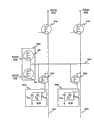
图1示出了使用TFT的典型有源矩阵LCD,有源矩阵LCD100。有源矩阵LCD100包括偏振器膜110、上玻璃基板120、滤色器130、透明电极140、液晶150、象素晶体管及连线(trace)160、边缘电子设备(edge electronics)170、下玻璃基板180以及偏振器膜190。总体来说,象素晶体管(及连线)170和下玻璃基板180可以称作底板,或者在这种情况下称作有源矩阵底板(即,透明(前)电极与液晶不是底板的一部分)。术语有源矩阵底板也可以用于指不包括边缘电子设备170的以上部件。这些层中的每一个彼此层叠,以便产生可以用于例如膝上计算机显示器的液晶显示器。在这种情况下,将可以添加框架从而支持LCD并且将显示器固定到膝上底座上。将使用电路从而允许从膝上计算机到LCD的通信,以便显示所希望的图形或视频。
当要通过有源矩阵显示器100进行图像显示时,使用TFT和边缘电子设备发送电信号,以便配置位于适当象素处的液晶从而使得没有光或者一部分光从象素透射。边缘电子设备可以包括:移位寄存器、将输出侧信号与显示器上的信号进行匹配的电平移位器(level shifter)以及输出缓冲器。图2示出了TFT和边缘电子设备的布局。图2包括:一组薄膜列晶体管210A至210n,一组薄膜行晶体管220A至220n,一组传导列连线240A至240n,一组传导行连线250A至250n,一组例如薄膜象素晶体管230的薄膜象素晶体管,以及一组例如象素260的象素。例如薄膜象素晶体管230的薄膜象素晶体管与每一行和列连线的交叉点相关联。象素与行和列连线的交叉点相关联。象素260提供象素的一个示例。因此,例如,当寻址到象素230时,适当的信号发送给薄膜列晶体管210A、薄膜行晶体管220A以及薄膜象素晶体管260。
目前,可以使用非晶硅薄膜晶体管(a-Si TFTs)或者多晶硅TFT(p-Si或者poly-Si TFTs)或者块硅(bulk-silicon)晶体管作为LCD显示器和其它类型的大多数显示器中的行、列以及象素晶体管。这些类型的晶体管的使用给显示器施加了一些设计限制。首先,与由a-Si或者poly-Si制造的晶体管相关联的性能极大地小于使用块硅的性能。块硅的使用通常不适用于象素晶体管,因为许多商用可变LCD或者其它显示器类型的尺寸大于用于制造传统的块硅晶体管的硅片的尺寸,并且对于用作象素底板而言,块硅的价格过高。另外,因为LCD基板必须清洁(clean),故用于制作块硅晶体管的硅片仅可以用作反射显示器的基板。第二,a-Si和poly-Si晶体管不具有用于行和列晶体管的足够性能,因此现有的LCD或其它显示器类型在板的边缘附近具有大量的互连,以便在集成电路中将行和列连线连接到使用晶体硅(例如,块硅)晶体管的外部电路。这些互连增加了电路和组装复杂性以及互连故障,并降低了制造产量。第三,a-Si和poly-Si电路的相对较大的尺寸和互连增加了显示器的重量。第四,因为需要相对较高的温度用于制造a-Si和poly-Si设备,透明基板的选择主要局限于使用玻璃、高温玻璃或者石英。
与使用块硅设备的电路相比较,需要改进了性能特性的电路,而且可以低成本应用于比典型硅片更大的区域以及与大量透明基板相兼容的温度。
此外,还需要可以集成到LCD板和其它显示器以便减小系统复杂度和重量的电路。
此外,还需要可以应用于例如塑料的柔性基板的电路。
发明内容
本发明涉及使用纳米线晶体管的显示器。具体地,描述了使用纳米线象素晶体管、纳米线行晶体管、纳米线列晶体管以及纳米线边缘电子设备的液晶显示器。纳米线象素晶体管用于控制施加于包含液晶的象素的电压。纳米线行晶体管对用于导通和截止位于沿与纳米线行对相连的行连线处的象素晶体管。纳米线列晶体管用于向位于沿连接到纳米线列晶体管的连线处的纳米线象素晶体管提供电压。纳米线边缘电子设备用于控制行和列晶体管。在可选的实施例中,提出了一种使用纳米线晶体管与用于象素、行和列晶体管以及边缘电子设备的其它形式晶体管相结合的液晶显示器。例如,使用非晶硅象素晶体管的液晶显示器配备了纳米线晶体管,用于行和列晶体管。在本发明的可选实施例中,也提供了包括以下的显示器技术:有机发光二极管显示器(OLED)、纳米管场效应显示器、等离子体显示器、微反射镜显示器、微机电(MEMs)显示器、电致变色显示器以及使用纳米线晶体管的电泳显示器。
在显示器中使用纳米线晶体管具有很多优点。首先,纳米线晶体管可以定位于包括玻璃和塑料的多种基板上。结果是,可以在柔性基板上开发显示器,其使用柔软和/或可弯曲的显示器开展大量应用。其次,当与a-Si和poly-Si TFT相比较时,纳米线晶体管具有较好的性能,因此允许将与行和列晶体管相关联的边缘电子设备集成到行和列连线之间。这使得可以制造具有增长的平面尺寸与框架尺寸比的显示器,尤其是LCD,用于保持屏幕并降低外部控制电路的复杂度。此外,因为纳米线晶体管较小,其可以减少与通常较差的传统的a-Si或polySi TFT相关联的模糊,因为较大的a-Si或poly Si TFT趋向于对通过例如LCD的显示器反射或者透射的光的重要部分进行阻挡。对于类似OLED的发射显示器,较小的晶体管使得底板区域的大部分可以由直接在底板上构建的OLED所占据,而不是在象素晶体管的顶部建立OLED的更困难的工艺。
其它的实施例、特点以及本发明的优点,与本发明的各实施例的结果和操作一起,都在以下参考附图进行详细描述。
附图说明
参考附图对本发明进行描述。在附图中,相同的参考数字表示相同或者功能类似的部件。在附图中首次出现的部件由相应的参考数字最左边的数位表示。
图1是有源矩阵LCD的图示。
图2是TFT和用于寻址LCD内的象素的边缘电子设备的图示。
图3A是使用根据本发明实施例的纳米线晶体管的LCD的图示。
图3B是根据本发明实施例的使用纳米线晶体管LCD的详细部分的图示。
图4是据本发明实施例的在LCD内的4个纳米线象素晶体管的图示。
图5是据本发明实施例的在LCD内的一对纳米线行晶体管的图示。
图6是据本发明实施例的在LCD之内的两个纳米线列晶体管的图示。
具体实施方式
应该理解这里所描述的具体实现是本发明的示例,并且不表示局限于本发明的任何其它局限范围。实际上,为了简短,传统的电子设备、制造、半导体设备,纳米管、纳米棒、纳米线与纳米带技术,以及系统(以及系统的独立工作部件的部件)的其它功能方面可以不在此详细描述。此外,尽管为所讨论的具体实现设置了纳米线的数量和这些纳米线的间距,并不表示实现要局限于此,还可以使用大范围的纳米线数量和间距。另外,可以变化纳米线的尺寸和构成。所描述的实现不表示要进行局限,并且可以使用大范围的尺寸和部件。
如此处所使用,术语“纳米线”通常指延长的任何导体或半导材料,其包括至少一个小于500nm的横截面尺寸,并且优选小于100nm,并且具有大于10的长宽比(长度:宽度),优选大于50,并且更优选大于100。这种纳米线的示例包括类似以下所描述的半导体纳米线:公开的国际专利申请No.WO 02/17362、WO 02/48701和WO01/03208、碳纳米管以及类似尺寸的其它延长的导体或半导体结构。
尽管这里所描述的LCD模型主要基于与硅相关联的性质,可以使用纳米线的其它类型,包括半导体纳米线,其包括选自以下的半导体材料,例如,Si,Ge,Sn,Se,Te,B,C(包括金刚石),P,B-C,B-P(BP6),B-Si,Si-C,Si-Ge,Si-Sn以及Ge-Sn,SiC,BN/BP/BAs,AlN/AlP/AlAs/AlSb,GaN/GaP/GaAs/GaSb,InN/InP/InAs/InSb,BN/BP/BAs,AlN/AlP/AlAs/AlSb,GaN/GaP/GaAs/GaSb,InN/InP/InAs/InSb,ZnO/ZnS/ZnSe/ZnTe,CdS/CdSe/CdTe,HgS/HgSe/HgTe,BeS/BeSe/BeTe/MgS/MgSe,GeS,GeSe,GeTe,SnS,SnSe,SnTe,PbO,PbS,PbSe,PbTe,CuF,CuCl,CuBr,CuI,AgF,AgCl,AgBr,AgI,BeSiN2,CaCN2,ZnGeP2,CdSnAs2,ZnSnSb2,CuGeP3,CuSi2P3,(Cu,Ag)(Al,Ga,In,Tl,Fe)(S,Se,Te)2,Si3N4,Ge3N4,Al2O3,(Al,Ga,In)2(S,Se,Te)3,Al2CO,以及两个或者多个这种半导体的适当组合。
在特定方面,半导体可以包括掺杂剂,其来自包括以下内容的群:来自元素周期表的组III的p型掺杂剂;来自元素周期表的组V的n型掺杂剂;选自包括P、Al和In的组的p型掺杂剂;选自包括P、As和Sb的组的n型掺杂剂;来自元素周期表的组II的p型掺杂剂;选自包括Mg、Zn、Cd和Hg的组的p型掺杂剂;来自元素周期表的组IV的p型掺杂剂;选自包括C和Si的组的p型掺杂剂;或者选自包括Si、Ge、Sn、S、Se和Te的组的n型掺杂剂。本领域的普通技术人员很容易理解可以使用其它公知的半导体掺杂剂。
此外,纳米线可以包括碳纳米管,或者导体或半导体有机聚合材料(例如,并五苯以及过渡金属氧化物)。
因此,尽管出于演示目的,贯穿这里的说明称作术语“纳米线”,其表示此处的描述还包括纳米管的使用。纳米管可以形成于这里所描述的单独用于纳米管或与纳米管相结合的结合/薄膜中,从而提供这里所描述的特点和优点。此外,纳米管不需要包括纯碳,但可以包含例如硼等其它材料,正如通过本发明的技术之一所认识到的。
此外,注意本发明的纳米线的薄膜可以是“异类的(heterogeneous)”膜,其包括:半导体纳米线和/或纳米管,和/或不同的纳米线组合,和/或不同部件的任何组合和/或结构特性。例如,“异类膜”可以包括具有不同直径和长度的纳米线/纳米管,并且纳米管和/或“异类结构”纳米管具有不同的特性。
通过实质上“对准的”或“定向的”意味着在一组或一群纳米线中的大多数纳米线的纵轴被定向在单个方向的30度之内。尽管可以认为超过50%的大量纳米线即大多数,在不同的实施例中,可以认为60%、75%、80%、90%或者纳米线的其它百分比是如此定向的大多数。在特定的优选方面,纳米线的大多数被定向于所希望方向的10度以内。在附加的实施例中,纳米线的大多数可以定向在所希望方向的其它范围数以内,包括随机或各向同性地定向。
应该理解这里所进行的空间描述(例如,“以上”、“以下”、“上方”、“下方”、“顶部”、“底部”等)仅用于描述的目的,并且本发明的设备可以以任何方向或方式进行空间排列。
最后,在集中讨论LCD的示例显示类型的同时,本发明应用于具有使用电子设备驱动象素改变的底板的显示器技术的任何类型,包括但不限于有机发光二极管(OLED)显示器、掺杂纳米晶体的OLED、纳米管场效应显示器、等离子体显示器、微反射镜显示器、微机电(MEMs)显示器、电致变色显示器等等。
图3A提供了根据本发明的实施例的使用纳米线晶体管的LCD300。LCD 300包括一组纳米线列晶体管310A至310n、一组纳米线行晶体管对320A至320n、一组纳米线象素晶体管330A至330z、一组传导列连线340A至340z、一组行连线350A到350n和一组象素360A到360z。每一个纳米线列晶体管与沿自纳米线列晶体管延伸的列连线的一组纳米线象素晶体管相连接。例如,纳米线列晶体管310A与沿列连线340A的纳米线象素晶体管330A、330M和330S相连接。每一个纳米线行晶体管对与沿自纳米线行晶体管延伸的行连线的一组纳米线象素晶体管相连接。例如,纳米线行晶体管320A与沿行连线350A的一组纳米线象素晶体管相连接。纳米线象素晶体管与相应的象素相关联。例如,纳米线象素晶体管330A与象素360A相关联。
此外,纳米线边缘电子设备(在图3A中未示出)可以用于控制纳米线列、行以及象素晶体管。纳米线边缘电子设备还可以用于驱动目前使用纳米线制造的列、行以及象素晶体管。纳米线边缘电子设备可以包括纳米线移位寄存器、纳米线电平移位器以及纳米线缓冲器。纳米线移位寄存器指使用纳米线晶体管实现的移位寄存器。纳米线电平移位器指使用纳米线晶体管实现的电平移位器。纳米线缓冲器指使用纳米线移位器实现的缓冲器。可以使用纳米晶体管实现边缘电子设备的其它类型。
在操作中,当要改变象素的亮度时,向用于象素所在列的纳米线列晶体管施加电压。导通用于象素所在行的纳米线行晶体管,从而允许电流流向纳米线象素晶体管。当纳米象素晶体管导通时,电流流过纳米线象素晶体管,从而使得在该象素两端存在电压,其大约等于施加于列上以产生透射象素的希望光强的电压。
尽管图3A示出了其中列、行以及象素晶体管都是纳米线晶体管的实施例。在可选的实施例中,纳米线晶体管与a-Si或poly-Si晶体管的任意组合可以用于列、行以及象素晶体管。例如,在一个实施例中,象素晶体管可以是a-Si TFT或poly-Si TFT,并且行和列晶体管可以是纳米线晶体管。这是有益的代替,因为对于象素晶体管的性能要求相对较低,并且可以通过a-Si TFT容易地实现。在另一示例中,列晶体管可以是a-Si TFT或poly-Si TFT,并且行和象素晶体管可以是纳米线晶体管。在另一示例中,行晶体管可以是a-Si TFT或poly-Si TFT,并且列和象素晶体管可以是纳米线晶体管。在另一示例中,象素晶体管和行晶体管可以是a-Si TFT或poly-Si TFT,并且列晶体管可以是纳米线晶体管。在另一示例中,象素晶体管和列晶体管可以是a-Si TFT或poly-Si TFT,并且行晶体管可以是纳米线晶体管。
图3B提供了根据本发明实施例的LCD300的部分390的更详细的视图。图3B强调了使用纳米线晶体管的LCD的许多方面,即,一对纳米线行晶体管连接到每一个行连线,并且每一个象素具有与其相关联的电阻和电容,其影响对于晶体管的设计考虑。应该注意,行和列连线还具有与其相关联的、影响设计准则的电阻和电容。纳米线行晶体管322和324形成纳米线行晶体管对320A,并通过行连线350A与纳米线象素晶体管330A和330B相连接。正如根据以下图5的更详细的描述,纳米线行晶体管322和324用于导通和截止纳米线象素晶体管,例如纳米线象素晶体管330A和330B。
此外,图3B描述了每一个象素具有与该象素相关联的电容和电阻。例如,象素360A包括电容Clcd、电容Cs和电阻Rlcd。电容Clcd表示与象素360A内的液晶相关联的电容。电阻Rlcd表示与象素360A内的液晶相关联的电阻。电容Cs是存储电容,添加其以便提高性能。
根据这里的示教,相关领域的技术人员可以将纳米线晶体管加入LCD中,而不需大量实验。此外,尽管设计工具示出了对于纳米线晶体管的具体类型的使用,但示例并不意欲进行限制。相当的相关领域的技术人员将可以应用这里的示教和以下所讨论的设计工具中所使用的概念,从而利用大范围的具有变化特性的纳米线半导体来开发集成的LCD或者其它显示器类型,这些变化特性例如纳米晶体材料的类型、掺杂剂、线的数量以及定向。
发明人开发了纳米线LCD设计工具,以便说明针对驱动LCD的象素内的液晶的电子设备使用纳米线晶体管的可行性。工具包括用户界面、LCD设计输入部件、纳米线特性输入部件、晶体管需求引擎以及纳米线设计引擎。用户界面使得用户可以输入设计准则和显示结果。LCD设计输入部件采集关于LCD类型的信息(例如LCD尺寸、象素密度等)。纳米线特性输入部件采集关于纳米线特性的信息,包括尺寸、纳米线晶体材料、掺杂剂以及相关的性能特性。晶体管需求引擎产生行、列以及象素晶体管所需的性能需求。纳米线设计引擎接收晶体管需求引擎的输出作为输入,并确定具体应用所需的纳米线晶体管的类型。
纳米线LCD设计工具用于说明纳米线晶体管可以用于驱动LCD之内的象素。工具的使用也有利于识别与在LCD中使用纳米线晶体管相关联的独一无二的益处。
在分析中,对于纳米线性能使用了保守的估计。具体地,利用了块硅的大约一半典型值的表面迁移率(surface mobility)(μs),其中相对于用于与掺杂剂相关的迁移的减少的掺杂剂量,使用了适当的的标准(μs)。在其中栅极控制晶体管的导电率的沟道中,假设掺杂剂是Na=1017/cm3,并且在没有栅极控制的源极和漏极中,Nd=1019/cm3。沟道、源极和漏极的长度每一个都假设为10μm。这些假设是保守的,以便确保可以使用最低成本的平版印刷。
此外,假设使用环形的栅极,其意味着栅极触点围绕纳米线。此外,假设纳米线具有核壳(core shell)设计,二氧化硅围绕在纳米线核周围并且栅极涂敷在氧化物周围。使用这种方法,假设直径为60nm的硅核纳米线具有40nm厚的SiO2壳,使得纳米线具有140nm的总直径。最后,假设保守的阈值和驱动电压,使得阈值电压(Vt)假设为2伏且驱动电压(Vd)假设为5伏。用于a-Si和poly-Si晶体管的驱动电压通常较高。所使用的电压假设与典型集成电路内所使用的电压更一致。2002年9月30日提交的美国临时申请No.60/414,323以及2003年5月7日提交的No.60/468,276描述了纳米线半导体并提供了支持这些假设的性能数据,通过在此参考将其整体包含。注意可以制造类似的底板电子设备,而不需要保角(conformal)栅极和/或保角栅极氧化物。
LCD板的假设基于现有LCD板的典型特征。具体地,假设LCD板具有21英寸对角线显示器,其分辨率为1024×768RGB象素,刷新频率60Hz。对于每一个RGB象素,存在三种象素(红、绿和蓝)。因此,列间距可以约为110μm并且行间距可以约为330μm。假设一个pF的电容与每一个象素相关联。假设行连线是10μm宽且1μm厚的铝(Al)。假设使用超过0.5μm厚的SiO2制造行绝缘层。假设列连线也是10μm宽且2μm厚的铝(Al)。假设使用超过2μm厚的SiO2制造列绝缘层。对于行和列连线的参数的选择确定了连线的电阻和电容。反之,沿象素的连线的电阻和电容以及晶体管电容和电阻确定了可以切换的线有多快,以及在行、列和象素晶体管内需要什么性能等级。
根据这些LCD准则,所制造的工具的输出用于为列、行和象素晶体管定义需求。相关领域的技术人员将可以理解规定TFT晶体管尺寸的方法。见,例如Satoru Tomita等人1997年4月5日发表于Journal ofthe Society of Information Display第339-404页的文章Transistor Sizingfor AMLCD Integrated TFT Drive Circuits。具体地,对于象素晶体管,将需要所确定的导通电阻小于1.6M欧姆的模型,并且将需要大于835G欧姆的截止电阻用于象素晶体管。导通和介质电阻基于多种因素。具体地,需要高截止阻抗从而避免在象素中的不希望的闪变效应。为了避免闪变,象素两端的电容电压必须在刷新(假设60Hz的刷新频率)之间的16.6ms下降(coast)而没有明显泄漏。泄漏率是纳米线象素晶体管的截止电阻的函数。LCD电阻或晶体管中的泄漏将引起象素上的电压在刷新之间改变,其可以包括象素中不希望的闪变。为了分析的目的,假设象素上的电压在刷新之间不能进行超过10%的改变。另一方面,要求导通电阻足够低,以便允许象素在可用的时间内充电。考虑到这些准则得到了上述导通和截止电阻。
一旦这些电阻已知,即可确定所需的晶体管的纳米线的数量。针对假设对其进行确定的工具使用了具有可以满足设计限制的少到1个纳米线的纳米线象素晶体管。超过一个纳米线也可以接受。
图4提供了根据本发明的实施例的LCD中4个纳米线象素晶体管的图示。正如分析结果所建议的,图示描述了单线纳米线象素晶体管的使用。所示的LCD的部分包括4个单线纳米线象素晶体管410A、410B、410C以及410D;多个象素的部分包括绿象素420;行连线430以及列连线440。纳米线象素晶体管410C具有连接到透明导体的一端,例如与绿象素420相关联的氧化铟锡。氧化铟锡导体用于向液晶单元的一侧施加电压。纳米线象素晶体管的另一端连接到列连线440上。在这些连接点之间的一点上,纳米线象素晶体管410C连接到行连线430。该连接点用作纳米线象素晶体管410C的栅极。基板概念在于施加到行连线430的电压将导通和截止纳米线象素晶体管410C。在可选的实施例中,可以在纳米线象素晶体管中使用多于一个的纳米线。
此外,分析还产生了针对纳米线行晶体管的设计结果,其说明了使用纳米线晶体管作为行晶体管的可行性。工具的使用确定了对于行晶体管的当前的设计需求可以用包含至少150个纳米线的纳米线晶体管来满足。所考虑的另一问题是检查一对纳米线行晶体管是否适合于两个行连线之间。模型计算说明纳米线行晶体管对的尺寸明显小于行连线之间的距离(大约小于4-10%),因此纳米线晶体管可以容易地放置于行连线之间。
在可选的实施例中,可以使用较高迁移率的纳米线,因此每个晶体管需要更少的纳米线。此外,这些数字将根据所希望的象素尺寸而增减。
图5提供了在LCD内的一对纳米线行晶体管的图示。图示包括纳米线行晶体管510、纳米线行晶体管520、象素530、纳米线象素晶体管540、列连线550、行连线560、上连线570、栅极连线572、下连线574以及栅极连线576。纳米线行晶体管510包括纳米线组515。类似地,纳米线行晶体管520包括纳米线组525。纳米线行晶体管510和520用于导通和截止纳米线象素晶体管540。
纳米线行晶体管510具有与行连线560相连的纳米线组515的一侧,以及与上连线570相连的另一侧。上连线570连接到导通电压上。在集中充当晶体管栅极的纳米线组515上的这些连接之间的每一个纳米线上的点与栅极连线572相连接。
纳米线行晶体管520具有与行连线560相连的纳米线组525的一侧,以及与下连线574相连的另一侧。下连线574接地。在集中充当晶体管栅极的纳米线组525上的这些连接之间的每一个纳米线上的点连接到栅极连线576。
当要导通纳米象素晶体管560时,向栅极连线572施加栅极电压从而导通纳米线行晶体管510。同时将栅极连线576接地从而截止纳米线行晶体管520。结果是,栅极电压连接到纳米象素晶体管栅极545,从而导通纳米象素晶体管540。当要截止纳米象素晶体管510时,进行相反的过程。从栅极连线572去除栅极电压,从而截止纳米线行晶体管510。并且,同时向栅极连线576施加栅极电压,从而导通纳米线行晶体管520。结果是,纳米线象素晶体管栅极545的栅极电压变为接地电压从而截止纳米线象素晶体管540。
此外,分析还产生了针对纳米线列晶体管的设计结果,其说明了使用纳米线晶体管作为列晶体管的可行性。工具的使用确定了当前的设计需求可以用包含至少3000个纳米线的纳米线晶体管来满足。列晶体管比晶体管的其它类型需要更多的纳米线,因为由于其具有较短的充电时间从而要求列晶体管具有较低的导通电阻,并且列线具有大量的电容。正如在纳米线行晶体管的情况下,工具说明了纳米线晶体管将适合于列连线之间。在每一种情况下,要求满足性能准则的纳米线的具体数量将受如以上所讨论的纳米晶体材料类型、掺杂剂量级以及其它因素的影响。
图6提供了根据本发明的实施例的LCD内的两个纳米线列晶体管的图示。图示包括纳米线列晶体管610、纳米线列晶体管620、列连线630、视频连线640以及栅极连线650。纳米线列晶体管610包括纳米线组615。纳米线列晶体管610可以用于向连接到列连线630的纳米线象素晶体管施加电压。
纳米线列晶体管610具有与列连线630相连接的纳米线组615的一侧,以及与视频连线640相连接的另一侧。视频连线640连接到用于驱动与列连线630相连接的纳米线象素晶体管的高压上。该视频电压设置象素电压并因此设置象素的亮度。在共同作为晶体管栅极的纳米线组615上的这些连接之间的每一个纳米线上的点连接到栅极连线650。栅极连线650连接到用于导通和截止象素列的控制电路。
正如可以从图3A、3B、4、5和6中所观察到的,可以按一个方向放置纳米线。即,在这种情况下,所有纳米线都是水平的,使得在基板上的纳米线的放置比纳米线为多种方向时更容易。在2002年9月30日提交的美国临时申请No.60/414,323中描述了实现该类型定位的方法。另外,纳米线可以根据具体设计准则放置于其它方向。此外,用于形成象素、行和列晶体管的纳米线数量是设计准则的函数,可以包括但不局限于超过2个纳米线、超过10个纳米线、超过100个纳米线以及超过1000个纳米线。
此外,使用纳米线晶体管的显示器可以形成于具有大范围特性的下基板上,例如下玻璃基板180。具体地,用于下基板的材料可以包括但不局限于玻璃、塑料、聚合物、晶体、金属或者纸。此外,用于下基板的材料特性可以包括但不局限于是透明材料、半透明材料、不透明材料、彩色材料、对入射光线偏振的材料以及不对入射光线偏振的材料。最后,用于下基板的材料可以是“低温”材料,其具有可以包括但不局限于低于500华氏度、低于300华氏度、低于200华氏度以及低于100华氏度的熔化温度。
结论
已经给出了本发明的典型实施例。本发明不局限于这些示例。这里提出这些示例的是为了描述而不是限制。根据这里所包含的示教,可选方案(包括这里所描述内容的等价物、扩展、变体、偏离等)对于那些相关领域的技术人员很容易理解。这种可选方案在本发明的范围和实质之内。
Claims (45)
1.一种在显示器中使用的有源矩阵底板,包括:
多个象素;
多个列晶体管,其中所述多个列晶体管之内的列晶体管向多个象素晶体管的子集两端施加电压;和
多个行晶体管,其中所述多个行晶体管之内的至少两个行晶体管导通或截止对应的象素晶体管;
多个象素晶体管,其中在所述多个象素晶体管之内的象素晶体管控制在所述多个象素之内的相应象素,其中所述多个象素晶体管之内的每一个象素晶体管、所述多个列晶体管之内的每一个列晶体管以及所述多个行晶体管之内的每一个行晶体管是纳米线晶体管,所述纳米线晶体管包括在晶体管的源极和漏极之间延伸的多个纳米线,并且每一个纳米线晶体管包括足够至少以希望速度对象素进行充电和放电的平均数目的纳米线;以及
边缘电子设备,其控制所述列晶体管、所述行晶体管和所述象素晶体管中的一个或更多个,其中所述边缘电子设备包括多个纳米线晶体管,每个纳米线晶体管包括在该晶体管的第一源极和第一漏极之间延伸的多个纳米线。
2.根据权利要求1所述的有源矩阵底板,其特征在于每一个列纳米线晶体管包括至少在源极和漏极之间延伸的至少100个纳米线。
3.根据权利要求1所述的有源矩阵底板,其特征在于每一个行纳米线晶体管包括至少在源极和漏极之间延伸的至少100个纳米线。
4.根据权利要求1所述的有源矩阵底板,其特征在于纳米线边缘电子设备包括纳米线缓冲器。
5.根据权利要求1所述的有源矩阵底板,其特征在于纳米线边缘电子设备包括纳米线移位寄存器。
6.根据权利要求1所述的有源矩阵底板,其特征在于纳米线边缘电子设备包括纳米线电平移位器。
7.根据权利要求1所述的有源矩阵底板,其特征在于显示器是液晶显示器。
8.根据权利要求1所述的有源矩阵底板,其特征在于显示器是有机发光显示器OLED。
9.根据权利要求8所述的有源矩阵底板,其特征在于所述OLED包括纳米晶体。
10.根据权利要求1所述的有源矩阵底板,其特征在于显示器是电泳显示器。
11.根据权利要求1所述的有源矩阵底板,其特征在于显示器是等离子体显示器。
12.根据权利要求1所述的有源矩阵底板,其特征在于显示器是电致变色显示器。
13.根据权利要求1所述的有源矩阵底板,其特征在于显示器是微机电MEMs显示器。
14.根据权利要求1所述的有源矩阵底板,其特征在于显示器是微反射镜显示器。
15.根据权利要求1所述的有源矩阵底板,其特征在于显示器是场发射显示器。
16.根据权利要求15所述的有源矩阵底板,其特征在于显示器是纳米管场发射显示器。
17.根据权利要求1所述的有源矩阵底板,其特征在于显示器是刚性的。
18.根据权利要求1所述的有源矩阵底板,其特征在于显示器是柔性的。
19.根据权利要求1所述的有源矩阵底板,其特征在于显示器是非平面的。
20.根据权利要求1所述的有源矩阵底板,其特征在于所述纳米线具有核壳设计,其中二氧化硅生长在纳米线核周围并且栅极涂敷在氧化物周围。
21.根据权利要求20所述的有源矩阵底板,其特征在于所述纳米线还包括围绕所述纳米线的栅极触点。
22.一种具有下基板的液晶显示器,包括:
(a)多个象素;
(b)多个象素晶体管,其中所述多个象素晶体管之内的象素晶体管控制所述多个象素之内的相应象素;
(c)多个列晶体管,其中所述多个列晶体管之内的列晶体管向所述多个象素晶体管的子集两端施加电压;以及
(d)多个行晶体管,其中所述多个行晶体管之内的至少两个行晶体管导通和截止相应的象素晶体管,其中i)所述多个象素晶体管、ii)所述多个列晶体管以及iii)所述多个行晶体管中的至少之一是纳米线晶体管,所述纳米线晶体管包括在所述纳米线晶体管的源极和漏极之间延伸的多个纳米线,并且每一个纳米线晶体管包括足够至少以希望速度对象素进行充电和放电的平均数目的纳米线;以及
(e)边缘电子设备,其控制所述列晶体管、所述行晶体管和所述象素晶体管中的一个或更多个,其中所述边缘电子设备包括多个纳米线晶体管,每个纳米线晶体管包括在该晶体管的第一源极和第一漏极之间延伸的多个纳米线。
23.根据权利要求22所述的液晶显示器,其特征在于纳米线边缘电子设备包括纳米线缓冲器。
24.根据权利要求22所述的液晶显示器,其特征在于纳米线边缘电子设备包括纳米线移位寄存器。
25.根据权利要求22所述的液晶显示器,其特征在于纳米线边缘电子设备包括纳米线电平移位器。
26.根据权利要求22所述的液晶显示器,其特征在于所述多个象素晶体管之内的象素晶体管、所述多个列晶体管之内的列晶体管和所述多个行晶体管之内的行晶体管是纳米线晶体管。
27.根据权利要求22所述的液晶显示器,其特征在于i)所述多个象素晶体管、ii)所述多个列晶体管以及iii)所述多个行晶体管中的至少之一是a-Si薄膜晶体管。
28.根据权利要求22所述的液晶显示器,其特征在于i)所述多个象素晶体管、ii)所述多个列晶体管以及iii)所述多个行晶体管中的至少之一是体Si薄膜晶体管。
29.根据权利要求22所述的液晶显示器,其特征在于i)所述多个象素晶体管、ii)所述多个列晶体管以及iii)所述多个行晶体管中的至少之一是有机半导体。
30.根据权利要求22所述的液晶显示器,其特征在于i)所述多个象素晶体管、ii)所述多个列晶体管以及iii)所述多个行晶体管中的至少之一是多晶硅薄膜晶体管。
31.根据权利要求22的液晶显示器,其特征在于用于形成晶体管的纳米线是对准的平行线。
32.根据权利要求22的液晶显示器,其特征在于随机并且各向同性地对齐纳米线。
33.根据权利要求22所述的液晶显示器,其特征在于纳米线列晶体管位于列连线之间。
34.根据权利要求22所述的液晶显示器,其特征在于纳米线列晶体管位于与列连线共线处。
35.根据权利要求22所述的液晶显示器,其特征在于纳米线行晶体管位于行连线之间。
36.根据权利要求22所述的液晶显示器,其特征在于纳米线行晶体管位于与行连线共线处。
37.根据权利要求22所述的液晶显示器,其特征在于纳米线晶体管包括连接纳米线晶体管的源极和漏极的至少10个纳米线。
38.根据权利要求22所述的液晶显示器,其特征在于纳米线晶体管包括连接纳米线晶体管的源极和漏极的至少100个纳米线。
39.根据权利要求22所述的液晶显示器,其特征在于下基板是柔性材料。
40.根据权利要求22所述的液晶显示器,其特征在于下基板是具有熔化温度低于500华氏度的低温材料。
41.根据权利要求22所述的液晶显示器,其特征在于下基板是塑料。
42.根据权利要求22所述的液晶显示器,其特征在于下基板是半透明的材料。
43.根据权利要求22所述的液晶显示器,其特征在于所述纳米线包括核壳设计,其中二氧化硅生长在纳米线核周围并且栅极涂敷在氧化物周围。
44.一种在显示器内所使用的有源矩阵底板,包括:
多个象素;
多个非晶硅象素晶体管,其中所述多个象素晶体管之内的象素晶体管控制在所述多个象素之内的相应象素;
多个行晶体管,被配置成使电流能够流向所述象素晶体管;以及
多个列晶体管,其中所述多个列晶体管之内的列晶体管向所述多个象素晶体管的子集两端施加电压,并且其中所述多个象素晶体管之内的每一个列晶体管是纳米线晶体管,所述纳米线晶体管包括在晶体管的源极和漏极之间延伸的多个纳米线,每一个纳米线晶体管包括足够至少以希望速度对象素进行充电和放电的平均数目的纳米线;以及
边缘电子设备,其控制所述列晶体管、所述行晶体管和所述象素晶体管中的一个或更多个,其中所述边缘电子设备包括多个纳米线晶体管,每个纳米线晶体管包括在该晶体管的第一源极和第一漏极之间延伸的多个纳米线。
45.根据权利要求44所述的有源矩阵底板,其特征在于每一个纳米线晶体管包括至少在源极和漏极之间延伸的至少100个纳米线。
Applications Claiming Priority (8)
| Application Number | Priority Date | Filing Date | Title |
|---|---|---|---|
| US41432302P | 2002-09-30 | 2002-09-30 | |
| US41435902P | 2002-09-30 | 2002-09-30 | |
| US60/414,323 | 2002-09-30 | ||
| US60/414,359 | 2002-09-30 | ||
| US46827603P | 2003-05-07 | 2003-05-07 | |
| US60/468,276 | 2003-05-07 | ||
| US48880103P | 2003-07-22 | 2003-07-22 | |
| US60/488,801 | 2003-07-22 |
Related Parent Applications (1)
| Application Number | Title | Priority Date | Filing Date |
|---|---|---|---|
| CN 03825281 Division CN1703730A (zh) | 2002-09-30 | 2003-09-30 | 使用纳米线晶体管的集成显示器 |
Publications (1)
| Publication Number | Publication Date |
|---|---|
| CN102569349A true CN102569349A (zh) | 2012-07-11 |
Family
ID=32074643
Family Applications (1)
| Application Number | Title | Priority Date | Filing Date |
|---|---|---|---|
| CN201210040611XA Pending CN102569349A (zh) | 2002-09-30 | 2003-09-30 | 使用纳米线晶体管的集成显示器 |
Country Status (8)
| Country | Link |
|---|---|
| US (2) | US7102605B2 (zh) |
| EP (1) | EP1563480A4 (zh) |
| JP (1) | JP4669784B2 (zh) |
| KR (1) | KR101043578B1 (zh) |
| CN (1) | CN102569349A (zh) |
| CA (1) | CA2499944A1 (zh) |
| TW (1) | TWI354261B (zh) |
| WO (1) | WO2004032190A2 (zh) |
Families Citing this family (129)
| Publication number | Priority date | Publication date | Assignee | Title |
|---|---|---|---|---|
| US8958917B2 (en) * | 1998-12-17 | 2015-02-17 | Hach Company | Method and system for remote monitoring of fluid quality and treatment |
| US7454295B2 (en) | 1998-12-17 | 2008-11-18 | The Watereye Corporation | Anti-terrorism water quality monitoring system |
| US9056783B2 (en) * | 1998-12-17 | 2015-06-16 | Hach Company | System for monitoring discharges into a waste water collection system |
| US20110125412A1 (en) * | 1998-12-17 | 2011-05-26 | Hach Company | Remote monitoring of carbon nanotube sensor |
| EP2298968A3 (en) | 2000-08-22 | 2011-10-05 | President and Fellows of Harvard College | Method for growing nanowires |
| AU2002229046B2 (en) | 2000-12-11 | 2006-05-18 | President And Fellows Of Harvard College | Nanosensors |
| US7417782B2 (en) | 2005-02-23 | 2008-08-26 | Pixtronix, Incorporated | Methods and apparatus for spatial light modulation |
| US8920619B2 (en) | 2003-03-19 | 2014-12-30 | Hach Company | Carbon nanotube sensor |
| US7397455B2 (en) * | 2003-06-06 | 2008-07-08 | Samsung Electronics Co., Ltd. | Liquid crystal display backplane layouts and addressing for non-standard subpixel arrangements |
| GB0323285D0 (en) * | 2003-10-04 | 2003-11-05 | Koninkl Philips Electronics Nv | Device and method of making a device having a patterned layer on a flexible substrate |
| US7553371B2 (en) * | 2004-02-02 | 2009-06-30 | Nanosys, Inc. | Porous substrates, articles, systems and compositions comprising nanofibers and methods of their use and production |
| US8025960B2 (en) * | 2004-02-02 | 2011-09-27 | Nanosys, Inc. | Porous substrates, articles, systems and compositions comprising nanofibers and methods of their use and production |
| US20110039690A1 (en) * | 2004-02-02 | 2011-02-17 | Nanosys, Inc. | Porous substrates, articles, systems and compositions comprising nanofibers and methods of their use and production |
| US7532194B2 (en) * | 2004-02-03 | 2009-05-12 | Idc, Llc | Driver voltage adjuster |
| KR100708644B1 (ko) | 2004-02-26 | 2007-04-17 | 삼성에스디아이 주식회사 | 박막 트랜지스터, 이를 구비한 평판 표시장치, 박막트랜지스터의 제조방법, 평판 표시장치의 제조방법, 및도너 시트의 제조방법 |
| US6912082B1 (en) * | 2004-03-11 | 2005-06-28 | Palo Alto Research Center Incorporated | Integrated driver electronics for MEMS device using high voltage thin film transistors |
| WO2005094440A2 (en) * | 2004-03-18 | 2005-10-13 | Nanosys Inc. | Nanofiber surface based capacitors |
| JP2008507114A (ja) | 2004-04-27 | 2008-03-06 | ザ ボード オブ トラスティーズ オブ ザ ユニヴァーシティー オブ イリノイ | ソフトリソグラフィ用複合パターニングデバイス |
| CA2564220A1 (en) | 2004-04-30 | 2005-12-15 | Nanosys, Inc. | Systems and methods for nanowire growth and harvesting |
| US7785922B2 (en) | 2004-04-30 | 2010-08-31 | Nanosys, Inc. | Methods for oriented growth of nanowires on patterned substrates |
| US20050279274A1 (en) * | 2004-04-30 | 2005-12-22 | Chunming Niu | Systems and methods for nanowire growth and manufacturing |
| US7943491B2 (en) | 2004-06-04 | 2011-05-17 | The Board Of Trustees Of The University Of Illinois | Pattern transfer printing by kinetic control of adhesion to an elastomeric stamp |
| US7799699B2 (en) | 2004-06-04 | 2010-09-21 | The Board Of Trustees Of The University Of Illinois | Printable semiconductor structures and related methods of making and assembling |
| US8217381B2 (en) | 2004-06-04 | 2012-07-10 | The Board Of Trustees Of The University Of Illinois | Controlled buckling structures in semiconductor interconnects and nanomembranes for stretchable electronics |
| US7521292B2 (en) | 2004-06-04 | 2009-04-21 | The Board Of Trustees Of The University Of Illinois | Stretchable form of single crystal silicon for high performance electronics on rubber substrates |
| EP2650907A3 (en) | 2004-06-04 | 2014-10-08 | The Board of Trustees of the University of Illinois | Methods and devices for fabricating and assembling printable semiconductor elements |
| CA2572798A1 (en) * | 2004-07-07 | 2006-07-27 | Nanosys, Inc. | Systems and methods for harvesting and integrating nanowires |
| US8089152B2 (en) * | 2004-09-16 | 2012-01-03 | Nanosys, Inc. | Continuously variable graded artificial dielectrics using nanostructures |
| US8558311B2 (en) | 2004-09-16 | 2013-10-15 | Nanosys, Inc. | Dielectrics using substantially longitudinally oriented insulated conductive wires |
| US7365395B2 (en) * | 2004-09-16 | 2008-04-29 | Nanosys, Inc. | Artificial dielectrics using nanostructures |
| JP2008523590A (ja) | 2004-12-06 | 2008-07-03 | プレジデント・アンド・フェロウズ・オブ・ハーバード・カレッジ | ナノスケールワイヤベースのデータ格納装置 |
| US7116275B2 (en) | 2005-01-28 | 2006-10-03 | Lockheed Martin Corporation | Operationally reconfigurable array |
| US7999994B2 (en) | 2005-02-23 | 2011-08-16 | Pixtronix, Inc. | Display apparatus and methods for manufacture thereof |
| US8310442B2 (en) | 2005-02-23 | 2012-11-13 | Pixtronix, Inc. | Circuits for controlling display apparatus |
| US8519945B2 (en) | 2006-01-06 | 2013-08-27 | Pixtronix, Inc. | Circuits for controlling display apparatus |
| US8159428B2 (en) | 2005-02-23 | 2012-04-17 | Pixtronix, Inc. | Display methods and apparatus |
| US7746529B2 (en) | 2005-02-23 | 2010-06-29 | Pixtronix, Inc. | MEMS display apparatus |
| US7742016B2 (en) | 2005-02-23 | 2010-06-22 | Pixtronix, Incorporated | Display methods and apparatus |
| US7755582B2 (en) | 2005-02-23 | 2010-07-13 | Pixtronix, Incorporated | Display methods and apparatus |
| US8482496B2 (en) | 2006-01-06 | 2013-07-09 | Pixtronix, Inc. | Circuits for controlling MEMS display apparatus on a transparent substrate |
| US7675665B2 (en) | 2005-02-23 | 2010-03-09 | Pixtronix, Incorporated | Methods and apparatus for actuating displays |
| US7271945B2 (en) * | 2005-02-23 | 2007-09-18 | Pixtronix, Inc. | Methods and apparatus for actuating displays |
| US9158106B2 (en) | 2005-02-23 | 2015-10-13 | Pixtronix, Inc. | Display methods and apparatus |
| US9261694B2 (en) | 2005-02-23 | 2016-02-16 | Pixtronix, Inc. | Display apparatus and methods for manufacture thereof |
| US9082353B2 (en) | 2010-01-05 | 2015-07-14 | Pixtronix, Inc. | Circuits for controlling display apparatus |
| US20070205969A1 (en) | 2005-02-23 | 2007-09-06 | Pixtronix, Incorporated | Direct-view MEMS display devices and methods for generating images thereon |
| US9229222B2 (en) | 2005-02-23 | 2016-01-05 | Pixtronix, Inc. | Alignment methods in fluid-filled MEMS displays |
| KR101109623B1 (ko) * | 2005-04-07 | 2012-01-31 | 엘지디스플레이 주식회사 | 박막트랜지스터와 그 제조방법. |
| KR101145146B1 (ko) | 2005-04-07 | 2012-05-14 | 엘지디스플레이 주식회사 | 박막트랜지스터와 그 제조방법 |
| US20100227382A1 (en) | 2005-05-25 | 2010-09-09 | President And Fellows Of Harvard College | Nanoscale sensors |
| WO2006132659A2 (en) | 2005-06-06 | 2006-12-14 | President And Fellows Of Harvard College | Nanowire heterostructures |
| US7927948B2 (en) | 2005-07-20 | 2011-04-19 | Micron Technology, Inc. | Devices with nanocrystals and methods of formation |
| EP1750310A3 (en) * | 2005-08-03 | 2009-07-15 | Samsung Electro-Mechanics Co., Ltd. | Omni-directional reflector and light emitting diode adopting the same |
| US7575978B2 (en) | 2005-08-04 | 2009-08-18 | Micron Technology, Inc. | Method for making conductive nanoparticle charge storage element |
| US7989290B2 (en) | 2005-08-04 | 2011-08-02 | Micron Technology, Inc. | Methods for forming rhodium-based charge traps and apparatus including rhodium-based charge traps |
| US7692610B2 (en) * | 2005-11-30 | 2010-04-06 | Semiconductor Energy Laboratory Co., Ltd. | Display device |
| JP4500797B2 (ja) * | 2005-12-06 | 2010-07-14 | キヤノン株式会社 | キャパシタと電界効果型トランジスタとを有する回路装置及び表示装置 |
| US7608877B2 (en) | 2005-12-06 | 2009-10-27 | Canon Kabushiki Kaisha | Circuit device having capacitor and field effect transistor, and display apparatus therewith |
| US7741197B1 (en) | 2005-12-29 | 2010-06-22 | Nanosys, Inc. | Systems and methods for harvesting and reducing contamination in nanowires |
| CN101331590B (zh) * | 2005-12-29 | 2011-04-20 | 纳米系统公司 | 用于在有图案基底上取向生长纳米线的方法 |
| US7427201B2 (en) * | 2006-01-12 | 2008-09-23 | Green Cloak Llc | Resonant frequency filtered arrays for discrete addressing of a matrix |
| US8526096B2 (en) | 2006-02-23 | 2013-09-03 | Pixtronix, Inc. | Mechanical light modulators with stressed beams |
| JP4970997B2 (ja) | 2006-03-30 | 2012-07-11 | パナソニック株式会社 | ナノワイヤトランジスタの製造方法 |
| JP5060740B2 (ja) | 2006-05-26 | 2012-10-31 | シャープ株式会社 | 集積回路装置およびその製造方法、ならびに表示装置 |
| US7876489B2 (en) | 2006-06-05 | 2011-01-25 | Pixtronix, Inc. | Display apparatus with optical cavities |
| GB0611452D0 (en) * | 2006-06-12 | 2006-07-19 | Plastic Logic Ltd | Page refreshing e-reader |
| JP2009540333A (ja) | 2006-06-12 | 2009-11-19 | プレジデント アンド フェロウズ オブ ハーバード カレッジ | ナノセンサーおよび関連技術 |
| US7554621B2 (en) * | 2006-06-26 | 2009-06-30 | Panasonic Corporation | Nanostructured integrated circuits with capacitors |
| WO2008033303A2 (en) | 2006-09-11 | 2008-03-20 | President And Fellows Of Harvard College | Branched nanoscale wires |
| CN102324462B (zh) * | 2006-10-12 | 2015-07-01 | 凯博瑞奥斯技术公司 | 基于纳米线的透明导体及其应用 |
| US20080094853A1 (en) | 2006-10-20 | 2008-04-24 | Pixtronix, Inc. | Light guides and backlight systems incorporating light redirectors at varying densities |
| KR20090087467A (ko) * | 2006-11-07 | 2009-08-17 | 나노시스, 인크. | 나노와이어 성장 시스템 및 방법 |
| WO2008127314A1 (en) | 2006-11-22 | 2008-10-23 | President And Fellows Of Harvard College | High-sensitivity nanoscale wire sensors |
| CN104637954B (zh) | 2007-01-17 | 2018-02-16 | 伊利诺伊大学评议会 | 制造半导体基光学系统的方法 |
| US7852546B2 (en) | 2007-10-19 | 2010-12-14 | Pixtronix, Inc. | Spacers for maintaining display apparatus alignment |
| US9176318B2 (en) | 2007-05-18 | 2015-11-03 | Pixtronix, Inc. | Methods for manufacturing fluid-filled MEMS displays |
| WO2008097867A1 (en) * | 2007-02-07 | 2008-08-14 | Green Cloak Llc | Displays including addressable trace structures |
| US8183566B2 (en) * | 2007-03-01 | 2012-05-22 | Hewlett-Packard Development Company, L.P. | Hetero-crystalline semiconductor device and method of making same |
| US8367506B2 (en) | 2007-06-04 | 2013-02-05 | Micron Technology, Inc. | High-k dielectrics with gold nano-particles |
| KR100868941B1 (ko) * | 2007-07-20 | 2008-11-17 | 황장환 | 무촉매 탄소 나노 튜브를 이용한 유기 발광 디스플레이소자 및 그의 제조 방법 |
| KR100868940B1 (ko) * | 2007-07-20 | 2008-11-17 | 황장환 | 도핑된 탄소 나노 튜브를 이용한 유기 발광 디스플레이소자 및 그의 제조 방법 |
| JP2009134275A (ja) * | 2007-11-02 | 2009-06-18 | Sony Corp | カラー液晶表示装置組立体及び光変換装置 |
| US8273983B2 (en) * | 2007-12-21 | 2012-09-25 | Hewlett-Packard Development Company, L.P. | Photonic device and method of making same using nanowires |
| CN103872002B (zh) | 2008-03-05 | 2017-03-01 | 伊利诺伊大学评议会 | 可拉伸和可折叠的电子器件 |
| GB2459251A (en) | 2008-04-01 | 2009-10-21 | Sharp Kk | Semiconductor nanowire devices |
| US8248560B2 (en) | 2008-04-18 | 2012-08-21 | Pixtronix, Inc. | Light guides and backlight systems incorporating prismatic structures and light redirectors |
| WO2010005707A1 (en) | 2008-06-16 | 2010-01-14 | The Board Of Trustees Of The University Of Illinois | Medium scale carbon nanotube thin film integrated circuits on flexible plastic substrates |
| EP2304802B8 (en) * | 2008-07-18 | 2013-12-04 | Panasonic Corporation | Semiconductor material |
| US8886334B2 (en) | 2008-10-07 | 2014-11-11 | Mc10, Inc. | Systems, methods, and devices using stretchable or flexible electronics for medical applications |
| WO2010042653A1 (en) | 2008-10-07 | 2010-04-15 | Mc10, Inc. | Catheter balloon having stretchable integrated circuitry and sensor array |
| US8389862B2 (en) | 2008-10-07 | 2013-03-05 | Mc10, Inc. | Extremely stretchable electronics |
| JP5442234B2 (ja) | 2008-10-24 | 2014-03-12 | 株式会社半導体エネルギー研究所 | 半導体装置及び表示装置 |
| US8169679B2 (en) | 2008-10-27 | 2012-05-01 | Pixtronix, Inc. | MEMS anchors |
| US7884004B2 (en) * | 2009-02-04 | 2011-02-08 | International Business Machines Corporation | Maskless process for suspending and thinning nanowires |
| KR101706915B1 (ko) | 2009-05-12 | 2017-02-15 | 더 보드 오브 트러스티즈 오브 더 유니버시티 오브 일리노이 | 변형가능 및 반투과 디스플레이를 위한 초박형, 미세구조 무기발광다이오드의 인쇄 어셈블리 |
| ES2910086T3 (es) | 2009-05-19 | 2022-05-11 | Oned Mat Inc | Materiales nanoestructurados para aplicaciones de batería |
| WO2010138506A1 (en) | 2009-05-26 | 2010-12-02 | Nanosys, Inc. | Methods and systems for electric field deposition of nanowires and other devices |
| US8623288B1 (en) | 2009-06-29 | 2014-01-07 | Nanosys, Inc. | Apparatus and methods for high density nanowire growth |
| WO2011038228A1 (en) | 2009-09-24 | 2011-03-31 | President And Fellows Of Harvard College | Bent nanowires and related probing of species |
| WO2011041727A1 (en) | 2009-10-01 | 2011-04-07 | Mc10, Inc. | Protective cases with integrated electronics |
| JP6046491B2 (ja) | 2009-12-16 | 2016-12-21 | ザ ボード オブ トラスティーズ オブ ザ ユニヴァーシティー オブ イリノイ | コンフォーマル電子機器を使用した生体内での電気生理学 |
| US10441185B2 (en) | 2009-12-16 | 2019-10-15 | The Board Of Trustees Of The University Of Illinois | Flexible and stretchable electronic systems for epidermal electronics |
| US9936574B2 (en) | 2009-12-16 | 2018-04-03 | The Board Of Trustees Of The University Of Illinois | Waterproof stretchable optoelectronics |
| US8666471B2 (en) | 2010-03-17 | 2014-03-04 | The Board Of Trustees Of The University Of Illinois | Implantable biomedical devices on bioresorbable substrates |
| EP2531881A2 (en) | 2010-02-02 | 2012-12-12 | Pixtronix Inc. | Methods for manufacturing cold seal fluid-filled display apparatus |
| KR101659642B1 (ko) | 2010-02-02 | 2016-09-26 | 픽스트로닉스 인코포레이티드 | 디스플레이 장치를 제어하기 위한 회로 |
| US9442285B2 (en) | 2011-01-14 | 2016-09-13 | The Board Of Trustees Of The University Of Illinois | Optical component array having adjustable curvature |
| US9765934B2 (en) | 2011-05-16 | 2017-09-19 | The Board Of Trustees Of The University Of Illinois | Thermally managed LED arrays assembled by printing |
| WO2012166686A2 (en) | 2011-05-27 | 2012-12-06 | Mc10, Inc. | Electronic, optical and/or mechanical apparatus and systems and methods for fabricating same |
| WO2012167096A2 (en) | 2011-06-03 | 2012-12-06 | The Board Of Trustees Of The University Of Illinois | Conformable actively multiplexed high-density surface electrode array for brain interfacing |
| KR101979354B1 (ko) | 2011-12-01 | 2019-08-29 | 더 보오드 오브 트러스티스 오브 더 유니버시티 오브 일리노이즈 | 프로그램 변형을 실행하도록 설계된 과도 장치 |
| KR101963229B1 (ko) | 2011-12-05 | 2019-03-29 | 삼성전자주식회사 | 접을 수 있는 박막 트랜지스터 |
| US9554484B2 (en) | 2012-03-30 | 2017-01-24 | The Board Of Trustees Of The University Of Illinois | Appendage mountable electronic devices conformable to surfaces |
| US9457128B2 (en) | 2012-09-07 | 2016-10-04 | President And Fellows Of Harvard College | Scaffolds comprising nanoelectronic components for cells, tissues, and other applications |
| US9786850B2 (en) | 2012-09-07 | 2017-10-10 | President And Fellows Of Harvard College | Methods and systems for scaffolds comprising nanoelectronic components |
| US9171794B2 (en) | 2012-10-09 | 2015-10-27 | Mc10, Inc. | Embedding thin chips in polymer |
| US9134552B2 (en) | 2013-03-13 | 2015-09-15 | Pixtronix, Inc. | Display apparatus with narrow gap electrostatic actuators |
| WO2014165634A2 (en) * | 2013-04-05 | 2014-10-09 | President And Fellows Of Harvard College | Three-dimensional networks comprising nanoelectronics |
| US9379166B2 (en) * | 2014-11-04 | 2016-06-28 | Atom Nanoelectronics, Inc. | Active matrix light emitting diodes display module with carbon nanotubes control circuits and methods of fabrication |
| JP2015181166A (ja) * | 2015-04-14 | 2015-10-15 | 株式会社半導体エネルギー研究所 | 表示装置 |
| WO2016196673A1 (en) | 2015-06-01 | 2016-12-08 | The Board Of Trustees Of The University Of Illinois | Alternative approach to uv sensing |
| KR20180033468A (ko) | 2015-06-01 | 2018-04-03 | 더 보드 오브 트러스티즈 오브 더 유니버시티 오브 일리노이 | 무선 전력 및 근거리 통신기능을 갖는 소형화된 전자 시스템 |
| US10925543B2 (en) | 2015-11-11 | 2021-02-23 | The Board Of Trustees Of The University Of Illinois | Bioresorbable silicon electronics for transient implants |
| CN105373259B (zh) * | 2015-12-11 | 2018-11-27 | 上海中航光电子有限公司 | 一种阵列基板、显示面板及显示装置 |
| US10117305B2 (en) | 2016-05-09 | 2018-10-30 | Industrial Technology Research Institute | Driving system and method for planar organic electroluminescent device |
| CN111393159A (zh) * | 2020-04-04 | 2020-07-10 | 南开大学 | 一种数码可控打印izo纳米线电极的方法 |
| CN111333103B (zh) * | 2020-04-04 | 2022-03-15 | 南开大学 | 一种数码可控打印izo半导体纳米线的方法 |
| CN114647119B (zh) * | 2020-12-18 | 2023-10-13 | 京东方科技集团股份有限公司 | 调光结构和调光设备 |
| CN113140452A (zh) * | 2021-04-21 | 2021-07-20 | 北海惠科光电技术有限公司 | 氧化铟锡纳米线及其制备方法和薄膜晶体管 |
Family Cites Families (44)
| Publication number | Priority date | Publication date | Assignee | Title |
|---|---|---|---|---|
| JPS6392928A (ja) * | 1986-10-07 | 1988-04-23 | Matsushita Electric Ind Co Ltd | アクテイブ二重マトリクスカラ−液晶表示装置 |
| JP2572003B2 (ja) * | 1992-03-30 | 1997-01-16 | 三星電子株式会社 | 三次元マルチチャンネル構造を有する薄膜トランジスタの製造方法 |
| US5962863A (en) | 1993-09-09 | 1999-10-05 | The United States Of America As Represented By The Secretary Of The Navy | Laterally disposed nanostructures of silicon on an insulating substrate |
| JP3476241B2 (ja) * | 1994-02-25 | 2003-12-10 | 株式会社半導体エネルギー研究所 | アクティブマトリクス型表示装置の表示方法 |
| US5747928A (en) * | 1994-10-07 | 1998-05-05 | Iowa State University Research Foundation, Inc. | Flexible panel display having thin film transistors driving polymer light-emitting diodes |
| WO1997049132A1 (en) | 1996-06-20 | 1997-12-24 | Jeffrey Frey | Light-emitting semiconductor device |
| EP2189839A1 (en) * | 1997-10-31 | 2010-05-26 | Seiko Epson Corporation | Electrooptical apparatus and electronic device |
| CA2323879C (en) * | 1998-04-10 | 2007-01-16 | E Ink Corporation | Electronic displays using organic-based field effect transistors |
| US6140993A (en) * | 1998-06-16 | 2000-10-31 | Atmel Corporation | Circuit for transferring high voltage video signal without signal loss |
| US6256767B1 (en) | 1999-03-29 | 2001-07-03 | Hewlett-Packard Company | Demultiplexer for a molecular wire crossbar network (MWCN DEMUX) |
| US6459095B1 (en) | 1999-03-29 | 2002-10-01 | Hewlett-Packard Company | Chemically synthesized and assembled electronics devices |
| US6815218B1 (en) | 1999-06-09 | 2004-11-09 | Massachusetts Institute Of Technology | Methods for manufacturing bioelectronic devices |
| EP2239794A3 (en) | 1999-07-02 | 2011-03-23 | President and Fellows of Harvard College | Nanoscopic wire-based devices, arrays, and methods of their manufacture |
| US6438025B1 (en) | 1999-09-08 | 2002-08-20 | Sergei Skarupo | Magnetic memory device |
| RU2173003C2 (ru) | 1999-11-25 | 2001-08-27 | Септре Электроникс Лимитед | Способ образования кремниевой наноструктуры, решетки кремниевых квантовых проводков и основанных на них устройств |
| KR100360476B1 (ko) | 2000-06-27 | 2002-11-08 | 삼성전자 주식회사 | 탄소나노튜브를 이용한 나노 크기 수직 트랜지스터 및 그제조방법 |
| WO2002003472A2 (en) | 2000-06-29 | 2002-01-10 | California Institute Of Technology | Aerosol silicon nanoparticles for use in semiconductor device fabrication |
| US6798000B2 (en) | 2000-07-04 | 2004-09-28 | Infineon Technologies Ag | Field effect transistor |
| GB2364933B (en) * | 2000-07-18 | 2002-12-31 | Lg Electronics Inc | Method of horizontally growing carbon nanotubes |
| DE10036897C1 (de) * | 2000-07-28 | 2002-01-03 | Infineon Technologies Ag | Feldeffekttransistor, Schaltungsanordnung und Verfahren zum Herstellen eines Feldeffekttransistors |
| US6447663B1 (en) | 2000-08-01 | 2002-09-10 | Ut-Battelle, Llc | Programmable nanometer-scale electrolytic metal deposition and depletion |
| US7301199B2 (en) | 2000-08-22 | 2007-11-27 | President And Fellows Of Harvard College | Nanoscale wires and related devices |
| EP2298968A3 (en) | 2000-08-22 | 2011-10-05 | President and Fellows of Harvard College | Method for growing nanowires |
| AU2002229046B2 (en) | 2000-12-11 | 2006-05-18 | President And Fellows Of Harvard College | Nanosensors |
| US6423583B1 (en) | 2001-01-03 | 2002-07-23 | International Business Machines Corporation | Methodology for electrically induced selective breakdown of nanotubes |
| JP4663139B2 (ja) * | 2001-02-16 | 2011-03-30 | 株式会社半導体エネルギー研究所 | 半導体装置の作製方法 |
| US6593065B2 (en) | 2001-03-12 | 2003-07-15 | California Institute Of Technology | Method of fabricating nanometer-scale flowchannels and trenches with self-aligned electrodes and the structures formed by the same |
| TW554388B (en) | 2001-03-30 | 2003-09-21 | Univ California | Methods of fabricating nanostructures and nanowires and devices fabricated therefrom |
| US7084507B2 (en) | 2001-05-02 | 2006-08-01 | Fujitsu Limited | Integrated circuit device and method of producing the same |
| JP2003017508A (ja) * | 2001-07-05 | 2003-01-17 | Nec Corp | 電界効果トランジスタ |
| US6896864B2 (en) | 2001-07-10 | 2005-05-24 | Battelle Memorial Institute | Spatial localization of dispersed single walled carbon nanotubes into useful structures |
| NZ513637A (en) | 2001-08-20 | 2004-02-27 | Canterprise Ltd | Nanoscale electronic devices & fabrication methods |
| JP2005501404A (ja) | 2001-08-30 | 2005-01-13 | コーニンクレッカ フィリップス エレクトロニクス エヌ ヴィ | 磁気抵抗装置および電子装置 |
| JP2003202834A (ja) * | 2001-10-24 | 2003-07-18 | Semiconductor Energy Lab Co Ltd | 半導体装置およびその駆動方法 |
| US20040005258A1 (en) | 2001-12-12 | 2004-01-08 | Fonash Stephen J. | Chemical reactor templates: sacrificial layer fabrication and template use |
| US7049625B2 (en) | 2002-03-18 | 2006-05-23 | Max-Planck-Gesellschaft Zur Fonderung Der Wissenschaften E.V. | Field effect transistor memory cell, memory device and method for manufacturing a field effect transistor memory cell |
| US6872645B2 (en) | 2002-04-02 | 2005-03-29 | Nanosys, Inc. | Methods of positioning and/or orienting nanostructures |
| US20030189202A1 (en) | 2002-04-05 | 2003-10-09 | Jun Li | Nanowire devices and methods of fabrication |
| US6760245B2 (en) | 2002-05-01 | 2004-07-06 | Hewlett-Packard Development Company, L.P. | Molecular wire crossbar flash memory |
| US7358121B2 (en) | 2002-08-23 | 2008-04-15 | Intel Corporation | Tri-gate devices and methods of fabrication |
| US7115916B2 (en) * | 2002-09-26 | 2006-10-03 | International Business Machines Corporation | System and method for molecular optical emission |
| US7051945B2 (en) * | 2002-09-30 | 2006-05-30 | Nanosys, Inc | Applications of nano-enabled large area macroelectronic substrates incorporating nanowires and nanowire composites |
| US7067867B2 (en) | 2002-09-30 | 2006-06-27 | Nanosys, Inc. | Large-area nonenabled macroelectronic substrates and uses therefor |
| US7619562B2 (en) * | 2002-09-30 | 2009-11-17 | Nanosys, Inc. | Phased array systems |
-
2003
- 2003-09-30 CN CN201210040611XA patent/CN102569349A/zh active Pending
- 2003-09-30 WO PCT/US2003/030636 patent/WO2004032190A2/en active Search and Examination
- 2003-09-30 TW TW092127033A patent/TWI354261B/zh not_active IP Right Cessation
- 2003-09-30 KR KR1020057005419A patent/KR101043578B1/ko active IP Right Grant
- 2003-09-30 JP JP2005500327A patent/JP4669784B2/ja not_active Expired - Lifetime
- 2003-09-30 US US10/673,669 patent/US7102605B2/en not_active Expired - Lifetime
- 2003-09-30 EP EP03770551A patent/EP1563480A4/en not_active Withdrawn
- 2003-09-30 CA CA002499944A patent/CA2499944A1/en not_active Abandoned
-
2006
- 2006-07-21 US US11/490,630 patent/US7701428B2/en active Active
Also Published As
| Publication number | Publication date |
|---|---|
| KR20050053708A (ko) | 2005-06-08 |
| JP4669784B2 (ja) | 2011-04-13 |
| US20040135951A1 (en) | 2004-07-15 |
| US7102605B2 (en) | 2006-09-05 |
| TW200417947A (en) | 2004-09-16 |
| AU2003279043A1 (en) | 2004-04-23 |
| EP1563480A4 (en) | 2010-03-03 |
| EP1563480A2 (en) | 2005-08-17 |
| WO2004032190A2 (en) | 2004-04-15 |
| US20060256059A1 (en) | 2006-11-16 |
| CA2499944A1 (en) | 2004-04-15 |
| KR101043578B1 (ko) | 2011-06-23 |
| TWI354261B (en) | 2011-12-11 |
| US7701428B2 (en) | 2010-04-20 |
| WO2004032190A3 (en) | 2005-06-23 |
| JP2006501689A (ja) | 2006-01-12 |
Similar Documents
| Publication | Publication Date | Title |
|---|---|---|
| CN102569349A (zh) | 使用纳米线晶体管的集成显示器 | |
| CN1703730A (zh) | 使用纳米线晶体管的集成显示器 | |
| JP7432029B2 (ja) | 半導体装置 | |
| JP6453416B2 (ja) | 表示装置 | |
| CN101826520B (zh) | 半导体装置 | |
| US9076392B2 (en) | Display device and driving method thereof | |
| CN106782416A (zh) | 一种显示面板及显示装置 | |
| JP2018092161A (ja) | 表示装置およびその動作方法 | |
| Gelinck et al. | 3.1: Invited Paper: Rollable QVGA Active‐Matrix Displays Based on Organic Electronics | |
| AU2003279043B2 (en) | Integrated displays using nanowire transistors | |
| WO2005101354A2 (en) | Display circuit having asymmetrical nonlinear resistive elements |
Legal Events
| Date | Code | Title | Description |
|---|---|---|---|
| C06 | Publication | ||
| PB01 | Publication | ||
| C10 | Entry into substantive examination | ||
| SE01 | Entry into force of request for substantive examination | ||
| C02 | Deemed withdrawal of patent application after publication (patent law 2001) | ||
| WD01 | Invention patent application deemed withdrawn after publication |
Application publication date: 20120711 |