CN1245581A - Organic light emitting device containing protection layer - Google Patents
Organic light emitting device containing protection layer Download PDFInfo
- Publication number
- CN1245581A CN1245581A CN97181500A CN97181500A CN1245581A CN 1245581 A CN1245581 A CN 1245581A CN 97181500 A CN97181500 A CN 97181500A CN 97181500 A CN97181500 A CN 97181500A CN 1245581 A CN1245581 A CN 1245581A
- Authority
- CN
- China
- Prior art keywords
- layer
- organic light
- compound
- dopant
- emitting device
- Prior art date
- Legal status (The legal status is an assumption and is not a legal conclusion. Google has not performed a legal analysis and makes no representation as to the accuracy of the status listed.)
- Pending
Links
- 239000000463 material Substances 0.000 claims abstract description 137
- 238000000034 method Methods 0.000 claims abstract description 40
- CLYVDMAATCIVBF-UHFFFAOYSA-N pigment red 224 Chemical compound C=12C3=CC=C(C(OC4=O)=O)C2=C4C=CC=1C1=CC=C2C(=O)OC(=O)C4=CC=C3C1=C42 CLYVDMAATCIVBF-UHFFFAOYSA-N 0.000 claims abstract description 35
- 238000005401 electroluminescence Methods 0.000 claims abstract description 14
- AMGQUBHHOARCQH-UHFFFAOYSA-N indium;oxotin Chemical compound [In].[Sn]=O AMGQUBHHOARCQH-UHFFFAOYSA-N 0.000 claims abstract description 11
- 239000010410 layer Substances 0.000 claims description 393
- 150000001875 compounds Chemical class 0.000 claims description 108
- 239000002019 doping agent Substances 0.000 claims description 90
- 238000000151 deposition Methods 0.000 claims description 74
- 239000000758 substrate Substances 0.000 claims description 69
- 230000008021 deposition Effects 0.000 claims description 60
- -1 phthalocyanine compound Chemical class 0.000 claims description 45
- 125000000217 alkyl group Chemical group 0.000 claims description 38
- 125000003118 aryl group Chemical group 0.000 claims description 34
- 239000011241 protective layer Substances 0.000 claims description 27
- BHEPBYXIRTUNPN-UHFFFAOYSA-N hydridophosphorus(.) (triplet) Chemical compound [PH] BHEPBYXIRTUNPN-UHFFFAOYSA-N 0.000 claims description 23
- 239000006096 absorbing agent Substances 0.000 claims description 22
- 230000005525 hole transport Effects 0.000 claims description 21
- 229910052751 metal Inorganic materials 0.000 claims description 19
- 239000002184 metal Substances 0.000 claims description 19
- 238000004519 manufacturing process Methods 0.000 claims description 18
- 125000001997 phenyl group Chemical group [H]C1=C([H])C([H])=C(*)C([H])=C1[H] 0.000 claims description 17
- 229910052757 nitrogen Inorganic materials 0.000 claims description 16
- 229910052782 aluminium Inorganic materials 0.000 claims description 13
- COHYTHOBJLSHDF-UHFFFAOYSA-N indigo powder Natural products N1C2=CC=CC=C2C(=O)C1=C1C(=O)C2=CC=CC=C2N1 COHYTHOBJLSHDF-UHFFFAOYSA-N 0.000 claims description 13
- 229910052760 oxygen Inorganic materials 0.000 claims description 13
- 239000000126 substance Substances 0.000 claims description 12
- 229910003472 fullerene Inorganic materials 0.000 claims description 10
- 229910052733 gallium Inorganic materials 0.000 claims description 10
- 230000008569 process Effects 0.000 claims description 10
- 239000011777 magnesium Substances 0.000 claims description 9
- UFWIBTONFRDIAS-UHFFFAOYSA-N Naphthalene Chemical compound C1=CC=CC2=CC=CC=C21 UFWIBTONFRDIAS-UHFFFAOYSA-N 0.000 claims description 8
- XAGFODPZIPBFFR-UHFFFAOYSA-N aluminium Chemical compound [Al] XAGFODPZIPBFFR-UHFFFAOYSA-N 0.000 claims description 8
- 125000005605 benzo group Chemical group 0.000 claims description 8
- UVNXNSUKKOLFBM-UHFFFAOYSA-N imidazo[2,1-b][1,3,4]thiadiazole Chemical compound N1=CSC2=NC=CN21 UVNXNSUKKOLFBM-UHFFFAOYSA-N 0.000 claims description 8
- AWJUIBRHMBBTKR-UHFFFAOYSA-N isoquinoline Chemical compound C1=NC=CC2=CC=CC=C21 AWJUIBRHMBBTKR-UHFFFAOYSA-N 0.000 claims description 8
- 229910052725 zinc Inorganic materials 0.000 claims description 8
- 239000011701 zinc Substances 0.000 claims description 8
- GYHNNYVSQQEPJS-UHFFFAOYSA-N Gallium Chemical compound [Ga] GYHNNYVSQQEPJS-UHFFFAOYSA-N 0.000 claims description 7
- 229910052749 magnesium Inorganic materials 0.000 claims description 7
- COHYTHOBJLSHDF-BUHFOSPRSA-N indigo dye Chemical compound N\1C2=CC=CC=C2C(=O)C/1=C1/C(=O)C2=CC=CC=C2N1 COHYTHOBJLSHDF-BUHFOSPRSA-N 0.000 claims description 6
- 229910052738 indium Inorganic materials 0.000 claims description 6
- YTVNOVQHSGMMOV-UHFFFAOYSA-N naphthalenetetracarboxylic dianhydride Chemical compound C1=CC(C(=O)OC2=O)=C3C2=CC=C2C(=O)OC(=O)C1=C32 YTVNOVQHSGMMOV-UHFFFAOYSA-N 0.000 claims description 6
- HCHKCACWOHOZIP-UHFFFAOYSA-N Zinc Chemical compound [Zn] HCHKCACWOHOZIP-UHFFFAOYSA-N 0.000 claims description 5
- RBTKNAXYKSUFRK-UHFFFAOYSA-N heliogen blue Chemical compound [Cu].[N-]1C2=C(C=CC=C3)C3=C1N=C([N-]1)C3=CC=CC=C3C1=NC([N-]1)=C(C=CC=C3)C3=C1N=C([N-]1)C3=CC=CC=C3C1=N2 RBTKNAXYKSUFRK-UHFFFAOYSA-N 0.000 claims description 5
- 125000000623 heterocyclic group Chemical group 0.000 claims description 5
- 230000001681 protective effect Effects 0.000 claims description 5
- 229910052711 selenium Inorganic materials 0.000 claims description 5
- 229910052717 sulfur Inorganic materials 0.000 claims description 5
- 229910052714 tellurium Inorganic materials 0.000 claims description 5
- 125000000026 trimethylsilyl group Chemical group [H]C([H])([H])[Si]([*])(C([H])([H])[H])C([H])([H])[H] 0.000 claims description 5
- FYYHWMGAXLPEAU-UHFFFAOYSA-N Magnesium Chemical group [Mg] FYYHWMGAXLPEAU-UHFFFAOYSA-N 0.000 claims description 4
- DGEZNRSVGBDHLK-UHFFFAOYSA-N [1,10]phenanthroline Chemical compound C1=CN=C2C3=NC=CC=C3C=CC2=C1 DGEZNRSVGBDHLK-UHFFFAOYSA-N 0.000 claims description 4
- 125000002080 perylenyl group Chemical group C1(=CC=C2C=CC=C3C4=CC=CC5=CC=CC(C1=C23)=C45)* 0.000 claims description 4
- CSHWQDPOILHKBI-UHFFFAOYSA-N peryrene Natural products C1=CC(C2=CC=CC=3C2=C2C=CC=3)=C3C2=CC=CC3=C1 CSHWQDPOILHKBI-UHFFFAOYSA-N 0.000 claims description 4
- IEQIEDJGQAUEQZ-UHFFFAOYSA-N phthalocyanine Chemical compound N1C(N=C2C3=CC=CC=C3C(N=C3C4=CC=CC=C4C(=N4)N3)=N2)=C(C=CC=C2)C2=C1N=C1C2=CC=CC=C2C4=N1 IEQIEDJGQAUEQZ-UHFFFAOYSA-N 0.000 claims description 4
- 229910052799 carbon Inorganic materials 0.000 claims description 3
- 125000000547 substituted alkyl group Chemical group 0.000 claims description 3
- 235000000177 Indigofera tinctoria Nutrition 0.000 claims description 2
- 238000010438 heat treatment Methods 0.000 claims description 2
- 229940097275 indigo Drugs 0.000 claims description 2
- 230000003287 optical effect Effects 0.000 claims description 2
- APFVFJFRJDLVQX-UHFFFAOYSA-N indium atom Chemical compound [In] APFVFJFRJDLVQX-UHFFFAOYSA-N 0.000 claims 3
- OBKARQMATMRWQZ-UHFFFAOYSA-N naphthalene-1,2,5,6-tetracarboxylic acid Chemical compound OC(=O)C1=C(C(O)=O)C=CC2=C(C(O)=O)C(C(=O)O)=CC=C21 OBKARQMATMRWQZ-UHFFFAOYSA-N 0.000 claims 3
- 150000002500 ions Chemical class 0.000 claims 2
- 125000002524 organometallic group Chemical group 0.000 claims 2
- 239000001045 blue dye Substances 0.000 claims 1
- 239000012808 vapor phase Substances 0.000 claims 1
- 238000002347 injection Methods 0.000 abstract description 32
- 239000007924 injection Substances 0.000 abstract description 32
- 239000011368 organic material Substances 0.000 abstract description 8
- ABMLGFPCLXTCEI-UHFFFAOYSA-N 4,8-bis(1,3-dithiol-2-ylidene)-[1,2,5]thiadiazolo[3,4-f][2,1,3]benzothiadiazole Chemical compound S1C=CSC1=C(C=1C2=NSN=1)C1=NSN=C1C2=C1SC=CS1 ABMLGFPCLXTCEI-UHFFFAOYSA-N 0.000 abstract 2
- 150000003254 radicals Chemical class 0.000 description 39
- 230000006870 function Effects 0.000 description 24
- OKKJLVBELUTLKV-UHFFFAOYSA-N Methanol Chemical compound OC OKKJLVBELUTLKV-UHFFFAOYSA-N 0.000 description 15
- XKRFYHLGVUSROY-UHFFFAOYSA-N Argon Chemical compound [Ar] XKRFYHLGVUSROY-UHFFFAOYSA-N 0.000 description 14
- VYPSYNLAJGMNEJ-UHFFFAOYSA-N Silicium dioxide Chemical compound O=[Si]=O VYPSYNLAJGMNEJ-UHFFFAOYSA-N 0.000 description 14
- 238000002360 preparation method Methods 0.000 description 14
- 239000000243 solution Substances 0.000 description 13
- XCJYREBRNVKWGJ-UHFFFAOYSA-N copper(II) phthalocyanine Chemical compound [Cu+2].C12=CC=CC=C2C(N=C2[N-]C(C3=CC=CC=C32)=N2)=NC1=NC([C]1C=CC=CC1=1)=NC=1N=C1[C]3C=CC=CC3=C2[N-]1 XCJYREBRNVKWGJ-UHFFFAOYSA-N 0.000 description 12
- 239000000975 dye Substances 0.000 description 12
- 239000011159 matrix material Substances 0.000 description 12
- 239000012044 organic layer Substances 0.000 description 12
- 230000003595 spectral effect Effects 0.000 description 12
- 239000010409 thin film Substances 0.000 description 12
- KFZMGEQAYNKOFK-UHFFFAOYSA-N Isopropanol Chemical compound CC(C)O KFZMGEQAYNKOFK-UHFFFAOYSA-N 0.000 description 11
- 238000010521 absorption reaction Methods 0.000 description 10
- 239000010408 film Substances 0.000 description 10
- 239000011521 glass Substances 0.000 description 10
- 238000004891 communication Methods 0.000 description 9
- 239000003989 dielectric material Substances 0.000 description 9
- 238000001194 electroluminescence spectrum Methods 0.000 description 9
- 238000005424 photoluminescence Methods 0.000 description 9
- 150000003839 salts Chemical class 0.000 description 9
- 241000894007 species Species 0.000 description 9
- 238000001771 vacuum deposition Methods 0.000 description 9
- CSCPPACGZOOCGX-UHFFFAOYSA-N Acetone Chemical compound CC(C)=O CSCPPACGZOOCGX-UHFFFAOYSA-N 0.000 description 8
- IJGRMHOSHXDMSA-UHFFFAOYSA-N Atomic nitrogen Chemical compound N#N IJGRMHOSHXDMSA-UHFFFAOYSA-N 0.000 description 8
- BQCADISMDOOEFD-UHFFFAOYSA-N Silver Chemical compound [Ag] BQCADISMDOOEFD-UHFFFAOYSA-N 0.000 description 8
- QVGXLLKOCUKJST-UHFFFAOYSA-N atomic oxygen Chemical compound [O] QVGXLLKOCUKJST-UHFFFAOYSA-N 0.000 description 8
- 239000001257 hydrogen Substances 0.000 description 8
- 229910052739 hydrogen Inorganic materials 0.000 description 8
- 239000001301 oxygen Substances 0.000 description 8
- 229910052715 tantalum Inorganic materials 0.000 description 8
- GUVRBAGPIYLISA-UHFFFAOYSA-N tantalum atom Chemical compound [Ta] GUVRBAGPIYLISA-UHFFFAOYSA-N 0.000 description 8
- TVIVIEFSHFOWTE-UHFFFAOYSA-K tri(quinolin-8-yloxy)alumane Chemical compound [Al+3].C1=CN=C2C([O-])=CC=CC2=C1.C1=CN=C2C([O-])=CC=CC2=C1.C1=CN=C2C([O-])=CC=CC2=C1 TVIVIEFSHFOWTE-UHFFFAOYSA-K 0.000 description 8
- OAICVXFJPJFONN-UHFFFAOYSA-N Phosphorus Chemical compound [P] OAICVXFJPJFONN-UHFFFAOYSA-N 0.000 description 7
- XUIMIQQOPSSXEZ-UHFFFAOYSA-N Silicon Chemical compound [Si] XUIMIQQOPSSXEZ-UHFFFAOYSA-N 0.000 description 7
- GWEVSGVZZGPLCZ-UHFFFAOYSA-N Titan oxide Chemical compound O=[Ti]=O GWEVSGVZZGPLCZ-UHFFFAOYSA-N 0.000 description 7
- 229910052786 argon Inorganic materials 0.000 description 7
- 238000000576 coating method Methods 0.000 description 7
- 238000000295 emission spectrum Methods 0.000 description 7
- 230000005284 excitation Effects 0.000 description 7
- 238000000103 photoluminescence spectrum Methods 0.000 description 7
- 239000004033 plastic Substances 0.000 description 7
- 229920003023 plastic Polymers 0.000 description 7
- 230000009467 reduction Effects 0.000 description 7
- 229910052710 silicon Inorganic materials 0.000 description 7
- 239000010703 silicon Substances 0.000 description 7
- 229910052709 silver Inorganic materials 0.000 description 7
- 239000004332 silver Substances 0.000 description 7
- 239000002904 solvent Substances 0.000 description 7
- PWEBUXCTKOWPCW-UHFFFAOYSA-N squaric acid Chemical compound OC1=C(O)C(=O)C1=O PWEBUXCTKOWPCW-UHFFFAOYSA-N 0.000 description 7
- 238000012546 transfer Methods 0.000 description 7
- OGGKVJMNFFSDEV-UHFFFAOYSA-N 3-methyl-n-[4-[4-(n-(3-methylphenyl)anilino)phenyl]phenyl]-n-phenylaniline Chemical compound CC1=CC=CC(N(C=2C=CC=CC=2)C=2C=CC(=CC=2)C=2C=CC(=CC=2)N(C=2C=CC=CC=2)C=2C=C(C)C=CC=2)=C1 OGGKVJMNFFSDEV-UHFFFAOYSA-N 0.000 description 6
- HEMHJVSKTPXQMS-UHFFFAOYSA-M Sodium hydroxide Chemical compound [OH-].[Na+] HEMHJVSKTPXQMS-UHFFFAOYSA-M 0.000 description 6
- WYURNTSHIVDZCO-UHFFFAOYSA-N Tetrahydrofuran Chemical compound C1CCOC1 WYURNTSHIVDZCO-UHFFFAOYSA-N 0.000 description 6
- 230000008901 benefit Effects 0.000 description 6
- 230000000903 blocking effect Effects 0.000 description 6
- 229910052732 germanium Inorganic materials 0.000 description 6
- 239000003446 ligand Substances 0.000 description 6
- SJCKRGFTWFGHGZ-UHFFFAOYSA-N magnesium silver Chemical compound [Mg].[Ag] SJCKRGFTWFGHGZ-UHFFFAOYSA-N 0.000 description 6
- 238000004544 sputter deposition Methods 0.000 description 6
- 125000001424 substituent group Chemical group 0.000 description 6
- 229930185605 Bisphenol Natural products 0.000 description 5
- 239000000980 acid dye Substances 0.000 description 5
- 239000006117 anti-reflective coating Substances 0.000 description 5
- 238000006243 chemical reaction Methods 0.000 description 5
- 239000011248 coating agent Substances 0.000 description 5
- 239000003086 colorant Substances 0.000 description 5
- ZSWFCLXCOIISFI-UHFFFAOYSA-N endo-cyclopentadiene Natural products C1C=CC=C1 ZSWFCLXCOIISFI-UHFFFAOYSA-N 0.000 description 5
- 229920000642 polymer Polymers 0.000 description 5
- 239000002244 precipitate Substances 0.000 description 5
- ZUQDDQFXSNXEOD-UHFFFAOYSA-N quinoxalin-5-ol Chemical compound C1=CN=C2C(O)=CC=CC2=N1 ZUQDDQFXSNXEOD-UHFFFAOYSA-N 0.000 description 5
- 239000000377 silicon dioxide Substances 0.000 description 5
- 238000001228 spectrum Methods 0.000 description 5
- XLYOFNOQVPJJNP-UHFFFAOYSA-N water Chemical compound O XLYOFNOQVPJJNP-UHFFFAOYSA-N 0.000 description 5
- UOCLXMDMGBRAIB-UHFFFAOYSA-N 1,1,1-trichloroethane Chemical compound CC(Cl)(Cl)Cl UOCLXMDMGBRAIB-UHFFFAOYSA-N 0.000 description 4
- 239000007983 Tris buffer Substances 0.000 description 4
- 150000001450 anions Chemical class 0.000 description 4
- IISBACLAFKSPIT-UHFFFAOYSA-N bisphenol A Chemical compound C=1C=C(O)C=CC=1C(C)(C)C1=CC=C(O)C=C1 IISBACLAFKSPIT-UHFFFAOYSA-N 0.000 description 4
- 230000015556 catabolic process Effects 0.000 description 4
- 239000007850 fluorescent dye Substances 0.000 description 4
- 239000012458 free base Substances 0.000 description 4
- CHPZKNULDCNCBW-UHFFFAOYSA-N gallium nitrate Chemical compound [Ga+3].[O-][N+]([O-])=O.[O-][N+]([O-])=O.[O-][N+]([O-])=O CHPZKNULDCNCBW-UHFFFAOYSA-N 0.000 description 4
- GNPVGFCGXDBREM-UHFFFAOYSA-N germanium atom Chemical compound [Ge] GNPVGFCGXDBREM-UHFFFAOYSA-N 0.000 description 4
- 238000004020 luminiscence type Methods 0.000 description 4
- 230000007246 mechanism Effects 0.000 description 4
- 235000012239 silicon dioxide Nutrition 0.000 description 4
- 229910001316 Ag alloy Inorganic materials 0.000 description 3
- UHOVQNZJYSORNB-UHFFFAOYSA-N Benzene Chemical compound C1=CC=CC=C1 UHOVQNZJYSORNB-UHFFFAOYSA-N 0.000 description 3
- XMWRBQBLMFGWIX-UHFFFAOYSA-N C60 fullerene Chemical class C12=C3C(C4=C56)=C7C8=C5C5=C9C%10=C6C6=C4C1=C1C4=C6C6=C%10C%10=C9C9=C%11C5=C8C5=C8C7=C3C3=C7C2=C1C1=C2C4=C6C4=C%10C6=C9C9=C%11C5=C5C8=C3C3=C7C1=C1C2=C4C6=C2C9=C5C3=C12 XMWRBQBLMFGWIX-UHFFFAOYSA-N 0.000 description 3
- RTZKZFJDLAIYFH-UHFFFAOYSA-N Diethyl ether Chemical compound CCOCC RTZKZFJDLAIYFH-UHFFFAOYSA-N 0.000 description 3
- IAZDPXIOMUYVGZ-UHFFFAOYSA-N Dimethylsulphoxide Chemical compound CS(C)=O IAZDPXIOMUYVGZ-UHFFFAOYSA-N 0.000 description 3
- 108091006149 Electron carriers Proteins 0.000 description 3
- UFHFLCQGNIYNRP-UHFFFAOYSA-N Hydrogen Chemical compound [H][H] UFHFLCQGNIYNRP-UHFFFAOYSA-N 0.000 description 3
- YXFVVABEGXRONW-UHFFFAOYSA-N Toluene Chemical compound CC1=CC=CC=C1 YXFVVABEGXRONW-UHFFFAOYSA-N 0.000 description 3
- 239000002800 charge carrier Substances 0.000 description 3
- 229910052681 coesite Inorganic materials 0.000 description 3
- 229910052906 cristobalite Inorganic materials 0.000 description 3
- 238000006731 degradation reaction Methods 0.000 description 3
- 239000008367 deionised water Substances 0.000 description 3
- 229910021641 deionized water Inorganic materials 0.000 description 3
- 238000005137 deposition process Methods 0.000 description 3
- 230000009977 dual effect Effects 0.000 description 3
- 238000005516 engineering process Methods 0.000 description 3
- 239000011888 foil Substances 0.000 description 3
- 150000002431 hydrogen Chemical group 0.000 description 3
- IBHBKWKFFTZAHE-UHFFFAOYSA-N n-[4-[4-(n-naphthalen-1-ylanilino)phenyl]phenyl]-n-phenylnaphthalen-1-amine Chemical group C1=CC=CC=C1N(C=1C2=CC=CC=C2C=CC=1)C1=CC=C(C=2C=CC(=CC=2)N(C=2C=CC=CC=2)C=2C3=CC=CC=C3C=CC=2)C=C1 IBHBKWKFFTZAHE-UHFFFAOYSA-N 0.000 description 3
- ZUOUZKKEUPVFJK-UHFFFAOYSA-N phenylbenzene Natural products C1=CC=CC=C1C1=CC=CC=C1 ZUOUZKKEUPVFJK-UHFFFAOYSA-N 0.000 description 3
- 239000002243 precursor Substances 0.000 description 3
- 239000000047 product Substances 0.000 description 3
- 230000005855 radiation Effects 0.000 description 3
- 230000006798 recombination Effects 0.000 description 3
- 238000005215 recombination Methods 0.000 description 3
- 238000004528 spin coating Methods 0.000 description 3
- 229910052682 stishovite Inorganic materials 0.000 description 3
- YLQBMQCUIZJEEH-UHFFFAOYSA-N tetrahydrofuran Natural products C=1C=COC=1 YLQBMQCUIZJEEH-UHFFFAOYSA-N 0.000 description 3
- 238000002207 thermal evaporation Methods 0.000 description 3
- 239000004408 titanium dioxide Substances 0.000 description 3
- 229910052905 tridymite Inorganic materials 0.000 description 3
- 238000001429 visible spectrum Methods 0.000 description 3
- UJOBWOGCFQCDNV-UHFFFAOYSA-N 9H-carbazole Chemical compound C1=CC=C2C3=CC=CC=C3NC2=C1 UJOBWOGCFQCDNV-UHFFFAOYSA-N 0.000 description 2
- LFQSCWFLJHTTHZ-UHFFFAOYSA-N Ethanol Chemical compound CCO LFQSCWFLJHTTHZ-UHFFFAOYSA-N 0.000 description 2
- YXLXNENXOJSQEI-UHFFFAOYSA-L Oxine-copper Chemical compound [Cu+2].C1=CN=C2C([O-])=CC=CC2=C1.C1=CN=C2C([O-])=CC=CC2=C1 YXLXNENXOJSQEI-UHFFFAOYSA-L 0.000 description 2
- OFBQJSOFQDEBGM-UHFFFAOYSA-N Pentane Chemical compound CCCCC OFBQJSOFQDEBGM-UHFFFAOYSA-N 0.000 description 2
- JUJWROOIHBZHMG-UHFFFAOYSA-N Pyridine Chemical compound C1=CC=NC=C1 JUJWROOIHBZHMG-UHFFFAOYSA-N 0.000 description 2
- KAESVJOAVNADME-UHFFFAOYSA-N Pyrrole Chemical compound C=1C=CNC=1 KAESVJOAVNADME-UHFFFAOYSA-N 0.000 description 2
- 229910004205 SiNX Inorganic materials 0.000 description 2
- 238000000862 absorption spectrum Methods 0.000 description 2
- SMZOGRDCAXLAAR-UHFFFAOYSA-N aluminium isopropoxide Chemical compound [Al+3].CC(C)[O-].CC(C)[O-].CC(C)[O-] SMZOGRDCAXLAAR-UHFFFAOYSA-N 0.000 description 2
- PNEYBMLMFCGWSK-UHFFFAOYSA-N aluminium oxide Inorganic materials [O-2].[O-2].[O-2].[Al+3].[Al+3] PNEYBMLMFCGWSK-UHFFFAOYSA-N 0.000 description 2
- 150000001412 amines Chemical class 0.000 description 2
- 230000004888 barrier function Effects 0.000 description 2
- 239000002585 base Substances 0.000 description 2
- 230000015572 biosynthetic process Effects 0.000 description 2
- 235000010290 biphenyl Nutrition 0.000 description 2
- 239000004305 biphenyl Substances 0.000 description 2
- 230000008859 change Effects 0.000 description 2
- 238000010549 co-Evaporation Methods 0.000 description 2
- 239000004020 conductor Substances 0.000 description 2
- 125000000058 cyclopentadienyl group Chemical group C1(=CC=CC1)* 0.000 description 2
- 238000013461 design Methods 0.000 description 2
- 239000003599 detergent Substances 0.000 description 2
- 238000006471 dimerization reaction Methods 0.000 description 2
- 238000001035 drying Methods 0.000 description 2
- 230000000694 effects Effects 0.000 description 2
- 230000005281 excited state Effects 0.000 description 2
- 239000000706 filtrate Substances 0.000 description 2
- 229940044658 gallium nitrate Drugs 0.000 description 2
- 239000007789 gas Substances 0.000 description 2
- 229910052737 gold Inorganic materials 0.000 description 2
- 239000010931 gold Substances 0.000 description 2
- 125000004435 hydrogen atom Chemical group [H]* 0.000 description 2
- 229910010272 inorganic material Inorganic materials 0.000 description 2
- 239000011147 inorganic material Substances 0.000 description 2
- 229910052742 iron Inorganic materials 0.000 description 2
- 230000031700 light absorption Effects 0.000 description 2
- 239000007788 liquid Substances 0.000 description 2
- 125000000040 m-tolyl group Chemical group [H]C1=C([H])C(*)=C([H])C(=C1[H])C([H])([H])[H] 0.000 description 2
- 150000002680 magnesium Chemical class 0.000 description 2
- 229910021645 metal ion Inorganic materials 0.000 description 2
- 125000002496 methyl group Chemical group [H]C([H])([H])* 0.000 description 2
- 239000000203 mixture Substances 0.000 description 2
- 238000012986 modification Methods 0.000 description 2
- 230000004048 modification Effects 0.000 description 2
- 230000003647 oxidation Effects 0.000 description 2
- 238000007254 oxidation reaction Methods 0.000 description 2
- 238000000623 plasma-assisted chemical vapour deposition Methods 0.000 description 2
- 239000010453 quartz Substances 0.000 description 2
- 239000011541 reaction mixture Substances 0.000 description 2
- 229910052707 ruthenium Inorganic materials 0.000 description 2
- 229910052594 sapphire Inorganic materials 0.000 description 2
- 239000010980 sapphire Substances 0.000 description 2
- 239000002356 single layer Substances 0.000 description 2
- 239000007787 solid Substances 0.000 description 2
- 238000010561 standard procedure Methods 0.000 description 2
- 238000000859 sublimation Methods 0.000 description 2
- 229910052718 tin Inorganic materials 0.000 description 2
- RIOQSEWOXXDEQQ-UHFFFAOYSA-N triphenylphosphine Chemical compound C1=CC=CC=C1P(C=1C=CC=CC=1)C1=CC=CC=C1 RIOQSEWOXXDEQQ-UHFFFAOYSA-N 0.000 description 2
- 230000005641 tunneling Effects 0.000 description 2
- PIINXYKJQGMIOZ-UHFFFAOYSA-N 1,2-dipyridin-2-ylethane-1,2-dione Chemical compound C=1C=CC=NC=1C(=O)C(=O)C1=CC=CC=N1 PIINXYKJQGMIOZ-UHFFFAOYSA-N 0.000 description 1
- 125000001637 1-naphthyl group Chemical group [H]C1=C([H])C([H])=C2C(*)=C([H])C([H])=C([H])C2=C1[H] 0.000 description 1
- CSDQQAQKBAQLLE-UHFFFAOYSA-N 4-(4-chlorophenyl)-4,5,6,7-tetrahydrothieno[3,2-c]pyridine Chemical compound C1=CC(Cl)=CC=C1C1C(C=CS2)=C2CCN1 CSDQQAQKBAQLLE-UHFFFAOYSA-N 0.000 description 1
- ZRXVCYGHAUGABY-UHFFFAOYSA-N 4-bromo-n,n-bis(4-bromophenyl)aniline Chemical compound C1=CC(Br)=CC=C1N(C=1C=CC(Br)=CC=1)C1=CC=C(Br)C=C1 ZRXVCYGHAUGABY-UHFFFAOYSA-N 0.000 description 1
- QGICIDGCKPUALM-UHFFFAOYSA-N 4-ethynyl-n,n-bis(4-ethynylphenyl)aniline Chemical compound C1=CC(C#C)=CC=C1N(C=1C=CC(=CC=1)C#C)C1=CC=C(C#C)C=C1 QGICIDGCKPUALM-UHFFFAOYSA-N 0.000 description 1
- GVPZSYRAEBIWEP-UHFFFAOYSA-N 5,8-bis(methylcarbamoyl)naphthalene-1,4-dicarboxylic acid Chemical compound C1=CC(C(O)=O)=C2C(C(=O)NC)=CC=C(C(=O)NC)C2=C1C(O)=O GVPZSYRAEBIWEP-UHFFFAOYSA-N 0.000 description 1
- RJCHVBHJXJDUNL-UHFFFAOYSA-N 5,8-dicarbamoylnaphthalene-1,4-dicarboxylic acid Chemical compound C1=CC(C(O)=O)=C2C(C(=N)O)=CC=C(C(O)=N)C2=C1C(O)=O RJCHVBHJXJDUNL-UHFFFAOYSA-N 0.000 description 1
- QTBSBXVTEAMEQO-UHFFFAOYSA-M Acetate Chemical group CC([O-])=O QTBSBXVTEAMEQO-UHFFFAOYSA-M 0.000 description 1
- 229910000838 Al alloy Inorganic materials 0.000 description 1
- VHUUQVKOLVNVRT-UHFFFAOYSA-N Ammonium hydroxide Chemical compound [NH4+].[OH-] VHUUQVKOLVNVRT-UHFFFAOYSA-N 0.000 description 1
- OVOCFVNMDSFGFG-UHFFFAOYSA-N C1=CC(=CC=2C(=CC(=C(C12)C(=O)O)C(=O)O)C(=O)O)C(=O)O Chemical compound C1=CC(=CC=2C(=CC(=C(C12)C(=O)O)C(=O)O)C(=O)O)C(=O)O OVOCFVNMDSFGFG-UHFFFAOYSA-N 0.000 description 1
- DRSHXJFUUPIBHX-UHFFFAOYSA-N COc1ccc(cc1)N1N=CC2C=NC(Nc3cc(OC)c(OC)c(OCCCN4CCN(C)CC4)c3)=NC12 Chemical compound COc1ccc(cc1)N1N=CC2C=NC(Nc3cc(OC)c(OC)c(OCCCN4CCN(C)CC4)c3)=NC12 DRSHXJFUUPIBHX-UHFFFAOYSA-N 0.000 description 1
- DCERHCFNWRGHLK-UHFFFAOYSA-N C[Si](C)C Chemical group C[Si](C)C DCERHCFNWRGHLK-UHFFFAOYSA-N 0.000 description 1
- HPYIUKIBUJFXII-UHFFFAOYSA-N Cyclopentadienyl radical Chemical class [CH]1C=CC=C1 HPYIUKIBUJFXII-UHFFFAOYSA-N 0.000 description 1
- MYMOFIZGZYHOMD-UHFFFAOYSA-N Dioxygen Chemical compound O=O MYMOFIZGZYHOMD-UHFFFAOYSA-N 0.000 description 1
- 241000155250 Iole Species 0.000 description 1
- WHXSMMKQMYFTQS-UHFFFAOYSA-N Lithium Chemical compound [Li] WHXSMMKQMYFTQS-UHFFFAOYSA-N 0.000 description 1
- 229910002666 PdCl2 Inorganic materials 0.000 description 1
- XOLBLPGZBRYERU-UHFFFAOYSA-N SnO2 Inorganic materials O=[Sn]=O XOLBLPGZBRYERU-UHFFFAOYSA-N 0.000 description 1
- JFBZPFYRPYOZCQ-UHFFFAOYSA-N [Li].[Al] Chemical compound [Li].[Al] JFBZPFYRPYOZCQ-UHFFFAOYSA-N 0.000 description 1
- 238000002835 absorbance Methods 0.000 description 1
- 239000002253 acid Substances 0.000 description 1
- 230000032683 aging Effects 0.000 description 1
- OFCNXPDARWKPPY-UHFFFAOYSA-N allopurinol Chemical compound OC1=NC=NC2=C1C=NN2 OFCNXPDARWKPPY-UHFFFAOYSA-N 0.000 description 1
- 229910045601 alloy Inorganic materials 0.000 description 1
- 239000000956 alloy Substances 0.000 description 1
- 239000004411 aluminium Substances 0.000 description 1
- XEPMXWGXLQIFJN-UHFFFAOYSA-K aluminum;2-carboxyquinolin-8-olate Chemical compound [Al+3].C1=C(C([O-])=O)N=C2C(O)=CC=CC2=C1.C1=C(C([O-])=O)N=C2C(O)=CC=CC2=C1.C1=C(C([O-])=O)N=C2C(O)=CC=CC2=C1 XEPMXWGXLQIFJN-UHFFFAOYSA-K 0.000 description 1
- 239000000908 ammonium hydroxide Substances 0.000 description 1
- 229910021417 amorphous silicon Inorganic materials 0.000 description 1
- 125000000129 anionic group Chemical group 0.000 description 1
- 229910000411 antimony tetroxide Inorganic materials 0.000 description 1
- 239000007864 aqueous solution Substances 0.000 description 1
- 125000006615 aromatic heterocyclic group Chemical group 0.000 description 1
- 125000000732 arylene group Chemical group 0.000 description 1
- 230000009286 beneficial effect Effects 0.000 description 1
- HFACYLZERDEVSX-UHFFFAOYSA-N benzidine Chemical compound C1=CC(N)=CC=C1C1=CC=C(N)C=C1 HFACYLZERDEVSX-UHFFFAOYSA-N 0.000 description 1
- XSCHRSMBECNVNS-UHFFFAOYSA-N benzopyrazine Natural products N1=CC=NC2=CC=CC=C21 XSCHRSMBECNVNS-UHFFFAOYSA-N 0.000 description 1
- 230000005540 biological transmission Effects 0.000 description 1
- XZCJVWCMJYNSQO-UHFFFAOYSA-N butyl pbd Chemical compound C1=CC(C(C)(C)C)=CC=C1C1=NN=C(C=2C=CC(=CC=2)C=2C=CC=CC=2)O1 XZCJVWCMJYNSQO-UHFFFAOYSA-N 0.000 description 1
- 239000006229 carbon black Substances 0.000 description 1
- 239000011111 cardboard Substances 0.000 description 1
- 125000003636 chemical group Chemical group 0.000 description 1
- 239000003153 chemical reaction reagent Substances 0.000 description 1
- 238000004140 cleaning Methods 0.000 description 1
- 239000000470 constituent Substances 0.000 description 1
- 238000007796 conventional method Methods 0.000 description 1
- GBRBMTNGQBKBQE-UHFFFAOYSA-L copper;diiodide Chemical compound I[Cu]I GBRBMTNGQBKBQE-UHFFFAOYSA-L 0.000 description 1
- 229910052593 corundum Inorganic materials 0.000 description 1
- 230000007423 decrease Effects 0.000 description 1
- 230000003247 decreasing effect Effects 0.000 description 1
- 230000007547 defect Effects 0.000 description 1
- 230000001066 destructive effect Effects 0.000 description 1
- HPNMFZURTQLUMO-UHFFFAOYSA-N diethylamine Chemical compound CCNCC HPNMFZURTQLUMO-UHFFFAOYSA-N 0.000 description 1
- 229910001882 dioxygen Inorganic materials 0.000 description 1
- 238000000313 electron-beam-induced deposition Methods 0.000 description 1
- 230000002708 enhancing effect Effects 0.000 description 1
- 239000000284 extract Substances 0.000 description 1
- 230000005669 field effect Effects 0.000 description 1
- 238000001914 filtration Methods 0.000 description 1
- 229920002457 flexible plastic Polymers 0.000 description 1
- 150000002258 gallium Chemical class 0.000 description 1
- 230000009477 glass transition Effects 0.000 description 1
- PCHJSUWPFVWCPO-UHFFFAOYSA-N gold Chemical compound [Au] PCHJSUWPFVWCPO-UHFFFAOYSA-N 0.000 description 1
- 125000005842 heteroatom Chemical group 0.000 description 1
- 238000005286 illumination Methods 0.000 description 1
- 238000010348 incorporation Methods 0.000 description 1
- 239000011810 insulating material Substances 0.000 description 1
- 230000010354 integration Effects 0.000 description 1
- 230000009878 intermolecular interaction Effects 0.000 description 1
- 239000004973 liquid crystal related substance Substances 0.000 description 1
- 229910052744 lithium Inorganic materials 0.000 description 1
- 238000001755 magnetron sputter deposition Methods 0.000 description 1
- 238000002844 melting Methods 0.000 description 1
- 230000008018 melting Effects 0.000 description 1
- 238000001465 metallisation Methods 0.000 description 1
- 238000002156 mixing Methods 0.000 description 1
- BLFVVZKSHYCRDR-UHFFFAOYSA-N n-[4-[4-(n-naphthalen-2-ylanilino)phenyl]phenyl]-n-phenylnaphthalen-2-amine Chemical group C1=CC=CC=C1N(C=1C=C2C=CC=CC2=CC=1)C1=CC=C(C=2C=CC(=CC=2)N(C=2C=CC=CC=2)C=2C=C3C=CC=CC3=CC=2)C=C1 BLFVVZKSHYCRDR-UHFFFAOYSA-N 0.000 description 1
- 125000001624 naphthyl group Chemical group 0.000 description 1
- QJGQUHMNIGDVPM-UHFFFAOYSA-N nitrogen group Chemical group [N] QJGQUHMNIGDVPM-UHFFFAOYSA-N 0.000 description 1
- 238000005457 optimization Methods 0.000 description 1
- 238000013086 organic photovoltaic Methods 0.000 description 1
- 150000004866 oxadiazoles Chemical class 0.000 description 1
- 239000003973 paint Substances 0.000 description 1
- 239000011087 paperboard Substances 0.000 description 1
- 239000002245 particle Substances 0.000 description 1
- 238000002161 passivation Methods 0.000 description 1
- 230000008447 perception Effects 0.000 description 1
- KJOLVZJFMDVPGB-UHFFFAOYSA-N perylenediimide Chemical compound C=12C3=CC=C(C(NC4=O)=O)C2=C4C=CC=1C1=CC=C2C(=O)NC(=O)C4=CC=C3C1=C42 KJOLVZJFMDVPGB-UHFFFAOYSA-N 0.000 description 1
- 229920001610 polycaprolactone Polymers 0.000 description 1
- 229920000728 polyester Polymers 0.000 description 1
- 239000002861 polymer material Substances 0.000 description 1
- 229920001343 polytetrafluoroethylene Polymers 0.000 description 1
- 238000005381 potential energy Methods 0.000 description 1
- 239000000843 powder Substances 0.000 description 1
- 238000005086 pumping Methods 0.000 description 1
- UMJSCPRVCHMLSP-UHFFFAOYSA-N pyridine Natural products COC1=CC=CN=C1 UMJSCPRVCHMLSP-UHFFFAOYSA-N 0.000 description 1
- 125000004076 pyridyl group Chemical group 0.000 description 1
- 238000010791 quenching Methods 0.000 description 1
- 239000002994 raw material Substances 0.000 description 1
- 238000010992 reflux Methods 0.000 description 1
- 238000002390 rotary evaporation Methods 0.000 description 1
- PWEBUXCTKOWPCW-UHFFFAOYSA-L squarate Chemical compound [O-]C1=C([O-])C(=O)C1=O PWEBUXCTKOWPCW-UHFFFAOYSA-L 0.000 description 1
- 239000010935 stainless steel Substances 0.000 description 1
- 229910001220 stainless steel Inorganic materials 0.000 description 1
- 238000003756 stirring Methods 0.000 description 1
- 125000001544 thienyl group Chemical group 0.000 description 1
- 230000007704 transition Effects 0.000 description 1
- 239000012780 transparent material Substances 0.000 description 1
- CWMFRHBXRUITQE-UHFFFAOYSA-N trimethylsilylacetylene Chemical group C[Si](C)(C)C#C CWMFRHBXRUITQE-UHFFFAOYSA-N 0.000 description 1
- 238000007740 vapor deposition Methods 0.000 description 1
- 238000005406 washing Methods 0.000 description 1
- 229910009112 xH2O Inorganic materials 0.000 description 1
- 229910001845 yogo sapphire Inorganic materials 0.000 description 1
Images


Classifications
-
- B—PERFORMING OPERATIONS; TRANSPORTING
- B82—NANOTECHNOLOGY
- B82Y—SPECIFIC USES OR APPLICATIONS OF NANOSTRUCTURES; MEASUREMENT OR ANALYSIS OF NANOSTRUCTURES; MANUFACTURE OR TREATMENT OF NANOSTRUCTURES
- B82Y10/00—Nanotechnology for information processing, storage or transmission, e.g. quantum computing or single electron logic
-
- H—ELECTRICITY
- H10—SEMICONDUCTOR DEVICES; ELECTRIC SOLID-STATE DEVICES NOT OTHERWISE PROVIDED FOR
- H10K—ORGANIC ELECTRIC SOLID-STATE DEVICES
- H10K50/00—Organic light-emitting devices
- H10K50/10—OLEDs or polymer light-emitting diodes [PLED]
- H10K50/17—Carrier injection layers
-
- H—ELECTRICITY
- H10—SEMICONDUCTOR DEVICES; ELECTRIC SOLID-STATE DEVICES NOT OTHERWISE PROVIDED FOR
- H10K—ORGANIC ELECTRIC SOLID-STATE DEVICES
- H10K59/00—Integrated devices, or assemblies of multiple devices, comprising at least one organic light-emitting element covered by group H10K50/00
- H10K59/80—Constructional details
- H10K59/875—Arrangements for extracting light from the devices
- H10K59/878—Arrangements for extracting light from the devices comprising reflective means
-
- H—ELECTRICITY
- H10—SEMICONDUCTOR DEVICES; ELECTRIC SOLID-STATE DEVICES NOT OTHERWISE PROVIDED FOR
- H10K—ORGANIC ELECTRIC SOLID-STATE DEVICES
- H10K71/00—Manufacture or treatment specially adapted for the organic devices covered by this subclass
- H10K71/60—Forming conductive regions or layers, e.g. electrodes
-
- H—ELECTRICITY
- H10—SEMICONDUCTOR DEVICES; ELECTRIC SOLID-STATE DEVICES NOT OTHERWISE PROVIDED FOR
- H10K—ORGANIC ELECTRIC SOLID-STATE DEVICES
- H10K85/00—Organic materials used in the body or electrodes of devices covered by this subclass
- H10K85/30—Coordination compounds
- H10K85/321—Metal complexes comprising a group IIIA element, e.g. Tris (8-hydroxyquinoline) gallium [Gaq3]
- H10K85/324—Metal complexes comprising a group IIIA element, e.g. Tris (8-hydroxyquinoline) gallium [Gaq3] comprising aluminium, e.g. Alq3
-
- H—ELECTRICITY
- H10—SEMICONDUCTOR DEVICES; ELECTRIC SOLID-STATE DEVICES NOT OTHERWISE PROVIDED FOR
- H10K—ORGANIC ELECTRIC SOLID-STATE DEVICES
- H10K85/00—Organic materials used in the body or electrodes of devices covered by this subclass
- H10K85/30—Coordination compounds
- H10K85/321—Metal complexes comprising a group IIIA element, e.g. Tris (8-hydroxyquinoline) gallium [Gaq3]
- H10K85/326—Metal complexes comprising a group IIIA element, e.g. Tris (8-hydroxyquinoline) gallium [Gaq3] comprising gallium
-
- H—ELECTRICITY
- H10—SEMICONDUCTOR DEVICES; ELECTRIC SOLID-STATE DEVICES NOT OTHERWISE PROVIDED FOR
- H10K—ORGANIC ELECTRIC SOLID-STATE DEVICES
- H10K85/00—Organic materials used in the body or electrodes of devices covered by this subclass
- H10K85/60—Organic compounds having low molecular weight
- H10K85/615—Polycyclic condensed aromatic hydrocarbons, e.g. anthracene
- H10K85/621—Aromatic anhydride or imide compounds, e.g. perylene tetra-carboxylic dianhydride or perylene tetracarboxylic di-imide
-
- H—ELECTRICITY
- H10—SEMICONDUCTOR DEVICES; ELECTRIC SOLID-STATE DEVICES NOT OTHERWISE PROVIDED FOR
- H10K—ORGANIC ELECTRIC SOLID-STATE DEVICES
- H10K2102/00—Constructional details relating to the organic devices covered by this subclass
- H10K2102/10—Transparent electrodes, e.g. using graphene
- H10K2102/101—Transparent electrodes, e.g. using graphene comprising transparent conductive oxides [TCO]
- H10K2102/103—Transparent electrodes, e.g. using graphene comprising transparent conductive oxides [TCO] comprising indium oxides, e.g. ITO
-
- H—ELECTRICITY
- H10—SEMICONDUCTOR DEVICES; ELECTRIC SOLID-STATE DEVICES NOT OTHERWISE PROVIDED FOR
- H10K—ORGANIC ELECTRIC SOLID-STATE DEVICES
- H10K2102/00—Constructional details relating to the organic devices covered by this subclass
- H10K2102/301—Details of OLEDs
- H10K2102/302—Details of OLEDs of OLED structures
- H10K2102/3023—Direction of light emission
- H10K2102/3026—Top emission
-
- H—ELECTRICITY
- H10—SEMICONDUCTOR DEVICES; ELECTRIC SOLID-STATE DEVICES NOT OTHERWISE PROVIDED FOR
- H10K—ORGANIC ELECTRIC SOLID-STATE DEVICES
- H10K59/00—Integrated devices, or assemblies of multiple devices, comprising at least one organic light-emitting element covered by group H10K50/00
- H10K59/30—Devices specially adapted for multicolour light emission
- H10K59/32—Stacked devices having two or more layers, each emitting at different wavelengths
-
- H—ELECTRICITY
- H10—SEMICONDUCTOR DEVICES; ELECTRIC SOLID-STATE DEVICES NOT OTHERWISE PROVIDED FOR
- H10K—ORGANIC ELECTRIC SOLID-STATE DEVICES
- H10K59/00—Integrated devices, or assemblies of multiple devices, comprising at least one organic light-emitting element covered by group H10K50/00
- H10K59/80—Constructional details
- H10K59/805—Electrodes
- H10K59/8051—Anodes
-
- H—ELECTRICITY
- H10—SEMICONDUCTOR DEVICES; ELECTRIC SOLID-STATE DEVICES NOT OTHERWISE PROVIDED FOR
- H10K—ORGANIC ELECTRIC SOLID-STATE DEVICES
- H10K59/00—Integrated devices, or assemblies of multiple devices, comprising at least one organic light-emitting element covered by group H10K50/00
- H10K59/80—Constructional details
- H10K59/875—Arrangements for extracting light from the devices
- H10K59/876—Arrangements for extracting light from the devices comprising a resonant cavity structure, e.g. Bragg reflector pair
-
- H—ELECTRICITY
- H10—SEMICONDUCTOR DEVICES; ELECTRIC SOLID-STATE DEVICES NOT OTHERWISE PROVIDED FOR
- H10K—ORGANIC ELECTRIC SOLID-STATE DEVICES
- H10K59/00—Integrated devices, or assemblies of multiple devices, comprising at least one organic light-emitting element covered by group H10K50/00
- H10K59/80—Constructional details
- H10K59/8791—Arrangements for improving contrast, e.g. preventing reflection of ambient light
- H10K59/8792—Arrangements for improving contrast, e.g. preventing reflection of ambient light comprising light absorbing layers, e.g. black layers
-
- H—ELECTRICITY
- H10—SEMICONDUCTOR DEVICES; ELECTRIC SOLID-STATE DEVICES NOT OTHERWISE PROVIDED FOR
- H10K—ORGANIC ELECTRIC SOLID-STATE DEVICES
- H10K85/00—Organic materials used in the body or electrodes of devices covered by this subclass
- H10K85/20—Carbon compounds, e.g. carbon nanotubes or fullerenes
- H10K85/211—Fullerenes, e.g. C60
Abstract
The present invention is directed to organic light emitting devices comprised of a heterostructure for producing electroluminescence, wherein the heterostructure includes a protection layer between a hole transporting layer and an indium tin oxide anode layer. The hole injection enhancement layer may be comprised of 3,4,9,10-perylenetetracarboxylic dianhydride (PTCDA), bis(1,2,5-thiadiazolo)-p-quinobis(1,3-dithiole) (BTQBT), or other suitable, rigid organic materials. The present invention is further directed to methods of fabricating such devices, wherein the devices may include alternative combinations of materials for each of the layers included in the devices.
Description
Technical Field
The present invention relates to an organic light emitting device comprising a protective layer present between a hole transport layer and an ITO anode layer.
Technical Field
Organic Light Emitting Devices (OLEDs) are light emitting devices that are made up of several layers, one of which is made up of an organic material that can be made to electroluminesce by applying a voltage to the device, see c.w. tang et al, article "applied physical communication" (appl. phys. lett), 51, 913, (1987). Some OLEDs have been shown to have sufficient brightness, color gamut, and operating lifetime to be useful as a practical alternative to LCD-based full-color flat panel displays (see s.r. forrest, p.e. burrows, and m.e. thompson, in the "Laser Focus World" (Laser Focus World), p.1995, 2 months). In addition, since many of the thin films used in such devices are transparent in the visible light range, it is possible to realize a completely new type of display pixel in which red (R), green (G), and blue (B) emitting layers are arranged in a longitudinal laminated structure so as to provide a simple manufacturing method for manufacturing a display pixel having a small red, green, and blue pixel size and a large fill factor.
Transparent oleds (toled) have been reported to represent a significant trend towards achieving high resolution individually addressable stacks of red, green and blue pixel stages, see international patent applications PCT/US95/15790 and PCT/US 97/02681. The disclosed TOLED has a transparency of more than 70% when powered off and emits light efficiently (about 1% quantum efficiency) from both surfaces of the top and bottom devices when powered on. TOLEDs use transparent Indium Tin Oxide (ITO) as a hole injection electrode and a Mg-Ag-ITO layer for electron injection. In the disclosed device, the Mg-Ag-ITO electrode is used as a hole injection contact for the different color emitting OLEDs of the second stack on top of the TOLED. Each device of the stacked oled (soled) is composed of a longitudinal stack of multiple layers that can be individually addressed and emit its own characteristic color through the transparent organic layers, the transparent contact layers and the glass substrate, leaving the device to emit any color produced by changing the relative output of the red and blue emitting layers.
Thus, PCT/US95/15790 discloses an integrated OLED that can be individually varied and controlled in both color and brightness with an external power supply provided within a color tunable display device. In this regard, the article explains the principle of achieving integrated, full-color pixels and thus providing high image resolution, which is therefore possible because of the compact pixel size. Furthermore, the device can be manufactured using techniques that significantly reduce manufacturing costs as compared to the prior art.
Devices whose structure is based on the use of layers of organic photovoltaic materials generally rely on conventional mechanisms leading to light emission. This mechanism is generally based on radiative recombination of trapped charges. Specifically, an organic light emitting device includes at least two organic thin films separating the anode and cathode of the device. The material of one of these layers is specifically selected based on the ability of the material to transport holes ("hole transporting layer" denoted "HTL") and the material of one of the other layers is specifically selected based on the ability of the material to transport electrons ("electron transporting layer" denoted "ETL"). It is this structure that the device can be considered to be a diode with a forward bias when the potential applied to the anode is higher than the potential applied to the cathode. Under such bias conditions, the anode injects holes (positive charge carriers) into the hole transport layer, while the cathode injects electrons into the electron transport layer. The portion of the luminescent medium adjacent to the anode thus forms a hole injection and transport region, while the portion of the luminescent medium adjacent to the cathode forms an electron injection and transport region. The injected holes and electrons each migrate to the oppositely charged electrode. A fowler (Ftenkel) exciton is formed when an electron and a hole are located in the same molecule. This recombination of the short-lived state can be seen as a drop in electrons from the conduction potential energy to a valence band, accompanied by relaxation, preferably by a luminescence mechanism, under certain conditions. From the viewpoint of the operation principle of the conventional organic thin film device, the electroluminescent layer includes a light emitting region that receives mobile charge carriers (electrons and holes) from each electrode.
The material that produces the electroluminescent emission is typically the same material that functions as both the electron transporting layer and the hole transporting layer. Such devices are referred to as having a single heterostructure. Alternatively, the electroluminescent material may also be present in a separate emissive layer between the hole transporting layer and the electron transporting layer, the device being referred to as a double heterostructure.
The emissive material is present as a host material in either the electron transporting layer or the hole transporting layer, and in addition to this, the emissive material may also be present as a dopant contained within the host material. The materials are selected to be host and dopant materials so that there is efficient energy transfer between the host and dopant materials. The materials used to fabricate OLEDs are desirably capable of providing electroluminescence concentrated in a relatively narrow band near a selected spectral range, corresponding to one of the three primary colors red, green and blue, so that they can be used as color layers in OLEDs or SOLEDs. It is particularly desirable to be able to select compounds in which the emission can be altered by selectively changing substituents or modifying the structure of the material of the base that produces the emission. In addition, these materials are required to produce acceptable electrical properties for OLEDs. Again, such host and dopant materials can preferably be incorporated into the OLED by using raw materials that are readily incorporated into the hole transporting layer or the electron transporting layer using conventional techniques.
The demonstration of efficient electroluminescence produced by vacuum deposited molecular organic light emitting devices is of interest for their potential application in emissive flat displays. For use in low cost active matrix displays, it is desirable to exhibit device structures that can be electronically integrated with pixels. Conventional OLEDs are grown on transparent anodes such as ITO and the emitted light is visible through the substrate, integrated using, for example, silicon-based display driver devices. It is therefore desirable to develop OLEDs which emit light through the top transparent contact layer. Surface emitting polymer-based OLEDs with a top anode of transparent ITO and translucent Au or Al grown on silicon have been demonstrated, see article d.r. baigent et Al, "applied physical communication", 65, 2636 (1994); and H.H.Kim et al, "lightwave technology" (J.Lightwave Technol.) journal, 12, 2107 (1994).
Kim et al obtained similar integration of molecular OLEDs with silicon using a tunneling silicon dioxide interface. However, the tunneling interface increases the operating voltage of the device, and recently reported transparent TOLEDs can avoid this problem in structures, see the article by v.bulovic et al "Nature" (Nature)380, 29(1996), and the article by g.gu et al "applied physical communication" 68, 2606(1996), which can in principle be grown on silicon substrates. The TOLED anode forms an electrical contact, i.e., a "bottom contact," that directly contacts the substrate, whereas the display driver device employs n-channel field effect transistors (NFETs) such as amorphous silicon NFETs, which require the bottom contact of the OLED to be the cathode. This requires the fabrication of inverted oleds (ioleds), i.e. devices in which the order of the layers disposed on the substrate is reversed. For example, for a single heterostructure OLED, an electron injecting cathode layer is deposited on the substrate, an electron transporting layer is deposited on the cathode, a hole transporting layer is deposited on the electron transporting layer and a hole injecting anode layer is deposited on the hole transporting layer.
For example, it has been found that when an ITO layer is deposited directly on an organic layer or a Mg: Ag surface (which is typically deposited on several organic layers), the deposition rate may only be about 2-5 Å per minute, because the high energy particle beams used at higher ITO deposition rates can cause the organic layers to be very susceptible to damage, resulting in unacceptable severe degradation of the overall performance of the OLED.
Further, it is preferable if the hole injection performance of the hole injection layer can be improved. Copper phthalocyanine (CuPc) has been shown to act as an effective hole injection layer in conventional OLEDs, see article "applied physical communication" by s.a. vanslyke et al, 69, 2160(1996) and US patent US 4720432, and 3,4,9, 10-perylenetetracarboxylic dianhydride (PTCDA) was also previously known to be an effective hole injection layer, see article "applied physical communication" by p.e. burrows et al, 64, 2285(1994), article 210, 1(1996) by v.bulovic et al, and article 210, 13(1996) by v.bulovic et al, chemical physical "(chem.phys.). In addition, PTCDA (in which TTO electrodes are deposited on the surface of the film) is used in photodetector structures, as described in F.F.so et al, IEEE. electronics communications (IEEE. Trans. Electron. devices)36, 66(1989), which shows that this material is resistant to sputter deposition of ITO with minimal conductive performance degradation.
Conventional displays including LCDs (liquid crystal) and conventional OLED (organic light emitting device) displays have another disadvantage of not being well adapted to viewing in bright light environments. As shown in fig. 21, light R emitted by a strong light source L, such as the sun, may be reflected from one or more layers (primarily metal layers) of a conventional display D. The reflected light R interferes with the ability of the viewer V to view the information-containing light I generated by the display D, thereby reducing the perceived contrast of the image produced by the display D. Accordingly, there is a need for an OLED display with improved contrast for viewing in bright light environments.
Summary of The Invention
The present invention relates to an OLED and a method for its preparation comprising a heterostructure for producing electroluminescence, wherein the heterostructure comprises a layer present between a hole transport layer and an ITO anode layer, which enables the underlying organic layers to be protected from damage during the ITO sputter deposition process.
It is a feature of the present invention that the protective layer for an OLED not only protects the underlying organic layer, but the protective layer also functions as a hole injection enhancement layer. Examples of preferred embodiments of the present invention, wherein the protective layer also functions as a hole injection enhancement layer, as disclosed in 1997.5.29, filed U.S. patent application (serial No. 08/865491), include PTCDA or involve arylene-based compounds.
The invention further relates to an improved method of fabricating an ITO layer in an OLED wherein the deposition rate is increased from a lower initial deposition rate to a significantly higher deposition rate after the ITO layer is deposited to an effective thickness to prevent damage to underlying layers during the process of fabricating the ITO layer, more particularly, another aspect of the invention relates to a vacuum deposition method wherein the initial deposition rate is increased by a factor of about 5 to 10 after the layer thickness reaches about 50 to 200 Å, still further, this aspect of the invention relates to a method wherein the initial deposition rate is about 2 to 5 Å/min and the final deposition rate is at least about 50 to 60 Å/min.
The present invention further relates to a high contrast Transparent Organic Light Emitting Device (TOLED) display in which the contrast of the display is improved by minimizing display reflected light. This is achieved by using a display with a TOLED structure and by arranging a low reflection absorber behind the TOLED display. TOLEDs have a substantially transparent conductive layer and do not reflect light as the metal conductive layer of conventional OLEDs. The low reflection absorber disposed behind the TOLED display functions to absorb light passing through the TOLED. Most of the incident light on a TOLED display is absorbed by the low reflection absorber, with very little of the incident light being reflected back to the viewer. This arrangement provides an improved contrast of image display. The display of the present invention also exhibits an improved contrast of images of different colors.
The invention further relates to an OLED comprising a host material and a dopant compound, the combination of which can be used to produce emission that converges to a relatively narrow band around the wavelength of a pure color of one of the primary colors.
Additional objects and advantages of the present invention will become apparent to those skilled in the art upon examination of the following detailed description of the invention.
Drawings
Fig. 1 illustrates a representative IOLED for a single heterogeneous device.
FIG. 2 illustrates the positive bias current-voltage characteristics (I-V) in a 0.05mm IOLED with PTCDA and CuPc Protective Cap Layers (PCLs), the function of the cap layers as hole injection enhancement layers, and the electrical characteristics of the device without PCLs.
FIG. 3 illustrates the luminous intensity versus current (L-I) for the IOLED of FIG. 2.
FIG. 4 illustrates a structure similar to conventional Alq without a hole injection enhancement layer3I-V characteristic of EL emission spectrum shape of IOLED with hole injection enhancement layer compared to base OLED.
Fig. 5 illustrates the current-voltage relationship of an OLED with and without a 60 Å PTCDA layer between the ITO anode layer and the NPD hole transport layer.
FIG. 6 illustrates a cross-sectional view of an OLED having an ITO layer prepared in two steps, the first step being a low ITO deposition rate preparation and the second step being a relatively high ITO deposition rate preparation.
FIG. 7 illustrates the resistivity of a 1000 Å thick ITO layer deposited on glass at 200 ("standard cubic centimeters per minute") argon gas flow, 5 millitorr pressure, and 45 watts radio frequency power as a function of oxygen gas flow.
FIG. 8 illustrates the absorbance of a 1000 Å thick ITO layer deposited at 45 Watts RF power as a function of wavelength and oxygen flow (200 sccm argon flow, 5 mTorr pressure, 0.8 Å deposition rate per second on a glass substrate).
Fig. 9 illustrates the variation of the I-V characteristics (indicated by small circles) of the TOLED prepared with a higher ITO deposition rate compared to the I-V characteristics (dashed lines) of the TOLED prepared with an ITO layer prepared entirely at a low ITO deposition rate.
Fig. 10 illustrates a representative OLED for a single heterostructure device.
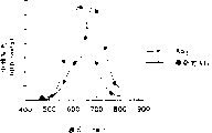
FIG. 11 illustrates Photoluminescence (PL) spectra of tris (5-hydroxy-quinoxaline) aluminum, tris (5-hydroxy-quinoline) aluminum and bis (5-hydroxy-quinoxaline) gallium.
FIG. 12 illustrates the electroluminescence spectra of OLEDs containing tris (5-hydroxy-quinoxaline) aluminum emissive layers with and without an inner salt of a bisphenyl squarate (squarium) compound of formula III as a dopant.
FIG. 13 illustrates the I-V characteristics of tris (5-hydroxy-quinoxaline) aluminum with and without an inner salt of a bisphenylsquaric acid (squarium) compound of formula VI as a dopant.
FIG. 14 illustrates the host compound Alq compared to the absorption spectrum of the dopant3And Alx3The dopant is diphenyl squaric acid inner salt dye ('BIS-OH'), an indigo dye and a fullerene compound, C60。
FIG. 15 illustrates photoluminescence spectra of dopants in solution, bis-phenyl squarate inner salt dye("BIS-OH") (in CH)2Cl2In (b), an indigo dye compound (in DMSO) and C60(in toluene).
FIG. 16 illustrates TPD-Alq3/C60Electroluminescent spectrum of device with host material Alq3C in60The relationship of the change in concentration increase.
FIG. 17 illustrates TPD-Alq3/(bisphenol squaric acid dye of general formula XI) electroluminescence spectra of the devices with host material Alq3The concentration of the dopant of the bisphenol squaric acid is changed.
FIG. 18 illustrates TPD-Alx3/(bisphenol squaric acid dye of formula XI) electroluminescence spectra of the device with host material Alx3The concentration of the dopant of the bisphenol squaric acid is changed.
FIG. 19 illustrates TPD-Alx3The electroluminescence spectrum of the indigo dye compound device, with a concentration of 1.7% of the indigo compound.
FIG. 20 illustrates representative compounds of formula XIII.
Fig. 21 illustrates a typical display device in a bright light environment.
Fig. 22 illustrates a high contrast TOLED display of the present invention in bright light environments.
Fig. 23 is a cross-sectional view of a first embodiment of the high contrast TOLED display of the present invention.
Fig. 24 is a cross-sectional view of a second embodiment of the high contrast TOLED display of the present invention.
Fig. 25 is a sectional view of a stacked light-emitting device of a first embodiment of the invention.
Fig. 26 is a sectional view of a stacked light-emitting device of a second embodiment of the invention.
Fig. 27 is a sectional view of a stacked light-emitting device of a third embodiment of the invention.
Fig. 28 is a cross-sectional view of one embodiment of an inverted stacked light emitting device of the present invention.
Fig. 29 illustrates an OLED with a distributed bragg reflector structure.
Detailed description of the preferred embodiments
The invention will now be described in detail with particular reference to certain preferred embodiments thereof, it being understood that these embodiments are provided by way of illustration and not of limitation.
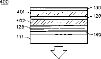
The inventive OLEDs comprise a heterostructure for producing electroluminescence, which can be produced as a single heterostructure or as a double heterostructure. A single or double heterostructure organic film material, and methods and apparatus for making the film are disclosed in U.S. patent No. 5554220, which is incorporated herein by reference. The term "electroluminescent-producing heterostructure" as used herein means a heterostructure comprising, in order for a single heterostructure: a hole injection anode layer, a hole transport layer, an electron transport layer and a cathode layer. There may be additional one or more layers between one or more of the pairs of layers. For example, for a double heterostructure, a separate emissive layer may be included between the hole transporting layer and the electron transporting layer.
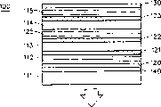
Either the anode layer or the cathode layer may contact the substrate and each electrode is in electrical contact connection capable of delivering a voltage across the device resulting in electroluminescence from the electron transport layer, the hole transport layer or a separate emissive layer. If the cathode layer is deposited on the substrate, the device may be said to have an Inverted OLED (IOLED) structure. The inverted OLED structure may also be referred to as an "OILED" structure. If the heterostructure producing electroluminescence is included as part of a stacked oled (soled), one or both electrodes of a single heterostructure may contact the electrodes of an adjoining heterostructure. Alternatively, an insulating layer may be provided between adjacent electrodes of the stacked OLEDs, depending on the circuitry used to drive the SOLED.
The term single or double heterostructure is intended herein only as an example to illustrate how an OLED embodying the invention can be made, but in no way limits the invention to the particular materials or order in which these layers are made as shown. For example, single heterostructures typically include: a substrate, which may be opaque or transparent, rigid or flexible, and/or plastic, metal or glass; a first electrode layer, typically a high work function hole injection anode layer, such as an Indium Tin Oxide (ITO) anode layer; a hole transport layer; an electron transport layer; and a second electrode layer, such as a low work function electron-injecting metal cathode layer, the metal being a magnesium silver alloy (Mg: Ag) or a lithium aluminum alloy (Li: Al).
Preferred materials that may be used as substrates in representative embodiments of the present invention include, in particular, glass, transparent polymers such as polyester, sapphire or quartz, or virtually any other material that may be used as a substrate for an OLED.
Preferred materials that may be used as the hole injection anode layer In representative embodiments of the present invention include, In particular, ITO, Zn-In-SnO2Or SbO2Or virtually any other material that can be used as an anode layer for hole injection in OLEDs.
Preferred materials that may be used as the hole transport layer in the representative embodiment of the present invention specifically include N, N '-diphenyl-N, N' -bis (3-tolyl) 1-1 'biphenyl-4, 4' diamine (TPD), 4, 4 '-bis [ N- (1-naphthyl) -N-phenyl-amino ] biphenyl (α -NPD) or 4, 4' -bis [ N- (2-naphthyl) -N-phenylamino ] biphenyl (β -NPD).
Preferred materials useful as electron transport layers include, in particular, tris (8-hydroxyquinoline) aluminum (Alq)3) And carbazole.
Preferred materials which can be used as the separate emissive layer, if present, include in particular dye-doped Alq3Or indeed any other material that can be used as the emissive layer of the OLED alone.
If an insulating layer is presentCan be made of an insulating material such as SiO2,SiNXOr Al2O3Or indeed any other material that can be used as an insulating layer in an OLED, can be deposited by various methods, such as Plasma Enhanced Chemical Vapor Deposition (PECVD) or electron beam deposition.
The OLEDs of the present invention may also include doped layers, such as those disclosed in "applied physics communications" (appl. phys. lett)70, 1665(1997) and Tang et al in the journal of applied physics (j.appl. phys.), 64, 3610(1989), which are incorporated herein by reference.
An advantage of the OLEDs of the present invention is that they can be manufactured entirely from vacuum deposited molecular organic materials, in contrast to, for example, OLEDs in which some of the layers are made from polymeric materials. Polymeric materials typically require solvent-based processes, such as spin-coating. Vacuum deposition methods, rather than solvent-based deposition of polymeric materials, are particularly suitable for use in fabricating the OLEDs of the present invention because they allow all vacuum deposition steps to be combined into a single sequential step through which the OLED is fabricated. Thus, this method does not require the use of solvents or the removal of air sensitive layers from the vacuum chamber, which exposes the layers to ambient conditions. The vacuum deposited material is one that can be deposited at a background pressure below atmospheric pressure, preferably about 10 deg.f-5-about 11-11Vacuum deposited material in torr.
Although there is no limitation to the range of layer thicknesses, the substrate may be 10 μm (microns) thin if it is a flexible plastic or metal foil substrate such as aluminum foil, or may be much thicker if it is a rigid, transparent or opaque substrate, or if it is constructed of a silicon-based display driver, and the ITO anode layer thickness is about 500 Å to greater than about 4000 Å (1 Å -10)-8cm), a hole transport layer of about 50 to greater than about 1000 Å, a single emissive layer of double heterostructure of about 50 to about 200 Å if present, an electron transport layer of about 50 to about 1000 Å, a metal cathode layer of about 50 to greater than about 100 Å, or much thicker if the cathode layer includes a silver protective layer and is opaque.
Thus, the layers present may in fact vary in type, number, thickness and order depending on whether the device comprises a single or double heterostructure, whether it is a SOLED or single OLED, whether it is a TOLED or IOLED, whether the OLED produces emission in a preferred spectral range, or whether other design variations are used.
However, the invention is particularly concerned with substantially any type of OLED structure having a protective layer between the hole transport layer and the anode layer. The invention relates in particular to OLEDs which comprise a protective layer which serves the function of a Protective Cap Layer (PCL) in order to reduce sputter damage to the underlying organic layers during the manufacture of the OLED. The invention further relates to an OLED comprising such a protective layer, which OLED has significantly enhanced hole injection efficiency properties. Enhanced hole injection efficiency is characterized by higher injection current at a given positive bias and/or higher maximum current before device failure. A "hole injection enhancement layer" is therefore a layer characterized by a current generation that is at least about 10%, typically about 50-100% or more higher than that of a device without such an additional layer. It is believed that such a layer generally provides an improved match to the energy levels of adjacent layers, resulting in enhanced hole injection.
The protective layer, which also functions to enhance the hole injection layer, may be formed by depositing, for example, the following compounds: a phthalocyanine compound or 3,4,9, 10-perylenetetracarboxylic dianhydride (PTCDA), of formula:
bis (1,2, 5-thiadiazolo) -p-quino-linobile (1, 3-dithiacyclopentadiene) (BTQBT), or other suitable rigid organic materials such as compounds of the general formula: 1, 4, 5, 8-naphthalene tetracarboxylic dianhydride (NTCDA):
 wherein R ═ hydrogen, alkyl, or aryl;
 wherein R ═ hydrogen, (1, 4, 5, 8-naphthalenetetracarboxylic diimide);
 wherein R ═ methyl, (N, N' -dimethyl-1, 4,5, 8-naphthalene tetracarboxylic acid diimide);
 wherein R ═ hydrogen, alkyl, or aryl;
 wherein R ═ hydrogen, (3, 4,9, 10-perylenetetracarboxylic diimide);
 wherein R ═ methyl, (N, N' -dimethyl-3, 4,9, 19-perylenetetracarboxylic diimide);
with the CA index name, bis-benzimidazolo [2, 1-a: 1 ', 2 ' -b ']Anthra (anthrac) [2, 1, 9-def: 6, 5, 10-d ' e ' f ']Di-isoquinoline-10, 21-dione;with the CA index name, bis-naphtho (bisnaphth) [2 ', 3',: 4,5]Imidazo [2, 1-a:2’,1’,-a’]Anthracno [2, 1, 9-def: 6, 5, 10-d ' e ' f ']Di-isoquinoline-10, 21-dione;
with the CA index name, bis-benzimidazolo [2, 1-b: 2 ', 1', -i]Benzo [ lmn ]][3,8]Phenanthroline-8, 1-dione;
with the CA index name, benzo [ lmn ] dinaphtho [2 ', 3': 4, 5] imidazo [2, 1-b: 2 ', 1' -I ] [3, 8] phenanthroline-9, 20-dione.
Any substituted derivative of these perylene, naphthalene, isoquinoline, phthalocyanine or phenanthroline based compounds, or family compounds, may also be used, all within the spirit of the present invention.
In a preferred embodiment, the cathode is deposited as an underlayer on a substrate on which the inverted OLED is deposited. Such inverted deposited OLEDs have the advantage of being fabricated entirely from vacuum deposited molecular organic materials, unlike, for example, OLEDs in which some of the layers are comprised of polymeric materials that cannot be conveniently deposited using vacuum deposition techniques. In inverted OLEDs containing polymers, a protective layer is generally not required because of the glass transition temperature (T) of the polymer materialg) Homomolecular organic materialT of (non-polymeric material)gWhich is much higher than usual and therefore more resistant to damage induced during ITO sputtering, such inverted OLEDs containing polymers cannot be conveniently fabricated using vacuum deposition techniques which allow for easy fabrication of the OLED. The protective cap layer is typically comprised of a crystalline organic layer that protects the underlying hole conducting material from damage during sputter deposition of the ITO anode.
The invention therefore relates to OLEDs which contain organic layers which are produced entirely from vacuum-deposited materials. Furthermore, the OLED of the present invention is comprised of a vacuum deposited molecular organic material containing a crystalline organic layer which not only protects the underlying hole transporting material from damage during sputter deposition of the ITO anode, but such layer also acts as a hole injection enhancement layer.
0.05mm2IOLED positive bias current-voltage characteristics (I-V) with PTCDA and CuPc PCLs are shown in FIG. 2, indicating that these characteristics are similar to conventional IOLEDs previously reported, where trap-limited conduction is observed, as reported by Z.Shen et al in "journal of applied Physics in Japan" (Jpn.J.appl.Phys.), 35, L401(1996), P.E.Burrows et al in "journal of applied Physics", 79, 7991(1996), (I α V)(m+1)). For an IOLED, m is 8, regardless of the specific device structure details or PCL thickness. The current density is 10mA/cm2The EL luminance of all devices is 40-100cd/m2Regardless of the details of the HTL, PCL, or anode structure, the IOLED featuring fig. 2 is a representative example of a device with different PTCDA or CuPc thicknesses the IOLED employing CuPc as the PCL has an operating voltage that is independent of the CuPc thickness between 40-170 Å, in contrast, the operating voltage of the PTCDA protected IOLED decreases sharply by 1.5V as the PTCDA thickness increases from 40 Å to 60 Å.
Although not intending to be a definite theoretical explanation of how hole injection is enhanced in PCL-containing OLEDs, it is believed that this enhancement is due in part to reduced damage to the vacuum deposited hole transport layer during deposition of the ITO layer and in part to reduced impediments to hole injection from the ITO into the hole injection enhancement layer.
The presence of PCL can also affect the maximum drive current (I) before device breakdownmax) In which IOLED without PCL only gets I of IOLED with PTCDA or CuPc PCL max10% of the total. FIGS. 2 and 3 confirm that ImaxThe difference is that all the IOLEDs are driven continuously at a higher current before breakdown of the device occurs.
Thus, it was shown that PCL protects the underlying organic material, lowers the operating voltage of IOLEDs and increases the I of PCL-containing fabricated IOLEDsmaxSimilar operating voltage reductions were also observed previously in conventional OLEDs with CuPc coated ITO anodes, see article by s.a. vanslyke et al in "applied physical communication", 69, 2160(1996) which is believed to be due to a reduced energy barrier for hole injection from ITO into CuPc as opposed to the energy barrier between ITO and HTL the lowest switching voltage (i.e. voltage equal to resistive conduction and trap-limited conduction) was obtained for iolds with PTCDA PCL having a thickness greater than 100 Å.
Fig. 3 shows the light intensity versus current (L-I) for the IOLED in fig. 2 the applied EL quantum efficiency of the protected IOLED is η ═ 0.15 ± 0.01% >, while the unprotected device is η ═ 0.30 ± 0.02% >, this difference is believed to be due in part to PCL absorption, since CuPc and PTCDA are both Alq at 530nm3For example, the thickness of CuPcPCL increased from 40 Å to 170 Å at η decreased by 25%. similarly, PTCDA protected IOLE increased from 10 Å to 120 Å for PTCDA thin film thicknessThe origin of the remaining difference between IOLEDs with and without PCL is not clear, although IT is generally believed that this is due to defects at the PTCDA/IT0 interface scattering some of the emitted light back into the PTCDA and can undergo another absorption therein3Different PCL materials (some of which are described above) whose emission is transparent, can somewhat enhance the efficiency of the IOLED. IOLEDs with PCLs have EL emission spectra shaped similarly to conventional Alq3OLEO-based (see fig. 4.) the IOLED spectrum with 60 Å thickness PTCDA PCL is slightly broader due to PCL absorption.
The results of fig. 5 show that a surface emitting, or Inverted Organic Led (IOLED), in which the cathode is bottom contacted and a new anode consisting of an organic hole injection PCL and a transparent, sputter deposited ITO film, can produce enhanced hole injection efficiency compared to an IOLED without such PCL. The IOLED can be grown on top of any smooth substrate to which the cathode will adhere, including opaque substrates such as silicon and metal foils. The I-V characteristics and EL spectra of IOLEDs are similar to those of conventional OLEDs, with higher operating voltages and somewhat reduced efficiency indicating further optimization of device contacts.
In particular, during the initial stages of the method of depositing ITO (which may cause substantial damage to the OLED), the deposition rate of ITO is preferably only about 2-5 Å per minute, although after the growing ITO layer reaches a certain threshold thickness sufficient to protect the underlying layer or layers, the deposition rate may increase several times, preferably to at least 5-10 times the initial deposition rate.
The RF power source used to prepare the ITO layer according to the method of the present invention is a high energy ATX-600 RF power source manufactured by Fort Collins, USA, and the power can be set at about 1W-7W for low ITO deposition rates and about 20-40W for high ITO deposition rates. Thus, during the transition from low ITO deposition rates to high ITO deposition rates, the power setting of the RF power supply is increased by as much as about 3-40 times. Preferably, this increase is at least about a 5-10 fold increase in the ITO deposition rate.
The underlying layer or layers may be a thin and relatively brittle magnesium silver cathode layer, an organic layer underlying the magnesium silver cathode layer, and/or an organic layer such as a hole transport layer, for example an ITO layer deposited directly thereon when fabricating an IOLED. As mentioned above, a low ITO deposition rate is a rate at which no particularly significant damage is detectable to the fragile layer, while a high ITO deposition rate is a rate at which significant damage is detectable to the fragile layer.
The ITO threshold thickness is the thickness sufficient to protect the underlying layer or layers from damage during the ITO deposition process, referred to herein as the "protective ITO layer," i.e., the thickness at which no particularly significant differences in the I-V characteristics of OLEDs manufactured using higher ITO deposition rates are observed, as compared to OLEDs manufactured using only low ITO deposition rates without damage. There is no particularly significant difference in the I-V characteristics, namely that the voltage required to obtain a particular current is within about 20% of the particular value observed for a particular OLED with non-destructive low ITO deposition rates for depositing ITO, over the entire range of voltages applied to the particular OLED structure.
The threshold thickness of the ITO growth layer required to protect the underlying layer may vary, depending on the actual material of the underlying layer, and this threshold thickness is preferably from about 50 to about 200 Å, and more preferably from about 50 to about 100 Å, the maximum rate of damage-free deposition used may vary widely depending on the actual material to be coated, and the deposition rate may be increased from about 2 to about 5 Å per minute to at least about 50 to about 60 Å per minute.
The performance of the OLED fabricated by the present invention can be evaluated by comparing the I-V characteristics of the OLED fabricated by the accelerated ITO deposition rate with that of the OLED fabricated by the deposition method using a single ITO deposition rate throughout. It has now been found that the accelerated deposition rate of ITO according to the present invention produces OLEDs having no particularly significant differences in I-V characteristics over OLEDs produced by an ITO deposition process that maintains a low deposition rate throughout.
In a preferred embodiment of the invention, the ITO layer is sputtered on the target using a radio frequency power supply in the presence of an oxygen flow, wherein the oxygen flow is selected to obtain the desired values of transparency and resistivity for a given ITO layer thickness. The actual oxygen flow selected may vary widely depending on the particular fabrication system used and is evaluated by the absorption of visible radiation by the ITO layer. In particular, it is preferred that the absorption of visible radiation (which varies with wavelength in the visible spectral range) be such that the total light transmission of an ITO layer fabricated using an accelerated deposition rate is comparable to that of ITO fabricated by low ITO deposition rate coating.
The range of variation of the oxygen flow is about 0.35-0.50sccm ("standard cm") for higher ITO deposition rates3Per minute) is 0 to up to about 0.2, preferably 0.1sccm for much lower ITO deposition rates. The performance of the ITO layers made using these methods was evaluated using these criteria and it was found that the I-V characteristics of the ITO coatings made using at least a 10-fold increase in ITO deposition rate were nearly equivalent compared to coatings made using only the lowest ITO deposition rate. Such an increase is typically obtained by setting the power of the rf power supply to 10 times greater.
In another aspect of the invention, the electron transport layer of an OLED made according to the present invention can include an organic radical, which can be suitable for preparing an electron transport layer for an OLEDThe method is used for manufacturing. In bookIn representative embodiments of the invention, the electron transport material may be represented by the chemical structure Cp of formula (I)ArThe expression, represents,
it can be considered to be a polyaryl-substituted cyclopentadienyl radical in which each Ar group, Ar1,Ar2,Ar3,Ar4And Ar5Is hydrogen, alkyl or a substituted or unsubstituted aromatic group. Although the term "Ar group" generally refers only to aryl groups, the term as used herein includes hydrogen or an alkyl group, although it is preferred that at most only one Ar group is hydrogen or an alkyl group and the remaining Ar groups are aromatic groups, most preferably all Ar groups are aromatic groups. The aromatic groups may each be chosen to be the same or different, the only limitation being placed on all compounds that may be encompassed by formula I as long as they are suitable for use in the preparation of an electron transport layer and the preparation of such compounds is chemically feasible. The organic radical compound defined herein is a material suitable for use as an electron transport layer as long as it can achieve a value of at least 10 per second for the carrier mobility of the electron transport layer-6cm2/V。
The substituted or unsubstituted aromatic group may be, for example, a phenyl group, a group having a condensed benzene ring such as a naphthyl group, or an aromatic heterocyclic group such as a pyridyl group or a thienyl group.
Each aromatic group may be unsubstituted or substituted with one or more substituents independently of the other aromatic group. The substituent or group may be an electron donating group, an electron accepting group or an alkyl group.
For those compounds that function not only as electron transport materials but also as emissive materials, substituted or unsubstituted aromatic groups can be selected to adjust the spectral emission characteristics to produce a desired color, such as can be characterized using the X-Y chromaticity coordinates of the CIE colorimetric system. For example, it is well known that substantial changes in the emission spectrum of phenyl-containing compounds can occur depending on whether the phenyl group is unsubstituted or substituted with electron donating or accepting groups in the ortho or para positions. In addition to being selected to tune the emission characteristics, the electron donating and electron accepting groups may also be selected to influence the extent of intermolecular interactions and thus carrier mobility. But also such substituents can be chosen so as to modulate the reduction potential of the organic radical, i.e. the energy required to reduce the radical, thereby converting the radical into the anion of the radical. By appropriate selection of the substituents in such a way that an easily accessible reduction potential is generated, the carrier mobility and/or carrier trap depth can advantageously be varied, so that stable organic radicals are generated which have an integrated electron transport and electron emission behavior and are particularly suitable for use as electron transport layers.
It is still more particularly established in the preferred embodiment that the organic radical is a pentaphenylcyclopentadienyl radical, CpφSee formula (II) below: wherein each aryl group of formula (I) is defined as a single phenyl group in formula (II) and is unsubstituted or independently substituted with R1、R2、R3、R4And R5And (b) substituted wherein each R group is independently one or more electron donating groups, electron accepting groups or alkyl groups.
In a specific illustrative embodiment of the present invention, the organic radical is unsubstituted Cp represented by the following general formula (III)φ·。
In another particular illustrative embodiment of the invention, the organic radical may be a tetraphenylcyclopentadienyl radical of the general formula (IV),
and it may be further substituted with changes, for example, hydrogen shown in the general formula (IV) may be substituted with an alkyl group.
While not intending to limit the organic free radicals disclosed in the representative embodiments to the theory of the present invention, it is believed that CpArThe effectiveness of free radicals as electron transport materials in the ETL of OLEDs is based on a combination of properties. They comprise a cyclopentadienyl ring which has a stereoshielding centre and which is capable of forming, as a result of the essentially complete stereoshielding of the cyclopentadienyl ringAn abnormally stable organic radical; the ability of cyclopentadienyl radicals to readily form anions that function with the radicals to act as electron carriers; the strongly aromatic character of cyclopentadienyl anions results in a strong overlap of the pi orbitals of the anion with those of the phenyl substituents, thus enhancing the electron mobility which promotes the effectiveness of the material as an electron carrier. It is another feature of the present invention that substituents included in the organic radicals can be selected to modify the emission spectrum and to modify the reduction potential of the radicals in a manner to obtain an overall combination of properties that are particularly suitable for use as an electron transport layer for electron transport and electron emission.
The invention therefore relates to an electron transport material suitable for use as an electron transport layer in an OLED, wherein the electron transport material consists of stable organic radicals having an easily acceptable reduction potential between the stable organic radicals and the anion formed by the radicals, such as pentaphenylcyclopentadienyl Cp of the general formula (III)φAnd pentaphenylcyclopentadienyl anions of the general formula (V):
an acceptable reduction potential results in suitable electron conduction through the electron transport layer, where suitable electron conduction is herein intended to mean an electron mobility of at least 10 per second-6cm2One electron conduction of/V.
Comprising CpφAn additional advantage provided by free-radical electron transport layers is that the electron transport material can in some cases act as an emissive material in the OLED. OLEDs can be fabricated with single heterostructures as long as the electron transporting material also functions as the emissive material. If the electron transporting material does not function as an emissive material, the OLED can be fabricated with a single heterostructure in which the hole transporting layer is the emissive layer or with a double heterostructure.
The invention further relates to a novel process for the preparation of Cp in integrated form as a thin layer of electron transporting material having high electron mobility and high electron carrier densityφFree radical processes in which the electron transport layer is included in a multilayer structure, in particular productionElectroluminescent heterostructures. It is believed that the prior art does not disclose an electron transport material composed of organic radicals. Thus, the present invention relates to the use of polyaryl-substituted cyclopentadienyl radicals, or more specifically polyphenyl-substituted cyclopentadienyl radicals, or even more specifically pentaphenylcyclopentadienyl radicals, as representative of preferred embodiments, it being understood that the present invention is generally directed to any organic radical that may be included in an electron transport layer for use as an electron transport material, so long as its electron mobility is at least 10 per second-6cm2/V。
In addition to being a free radical, CpφThe free radical being different from pentaphenylcyclopentadienyl itself, Cpφ H: Except that Cp has been reportedφH is a blue-emitting material when used in OLEDs, see C.Adachi et al in "applied physical communication", 56, 799-.
And CpφThe free radical being different from CpφH radicals, the latter not readily reducible. CpφBy loss of H after reduction+A stable anionic form is obtained, which is not energetically feasible. According to thisThere is no reason to expect Cp from some differencesφH has excellent carrier transport property, Cpφ-The radicals can be particularly well suited for this purpose.
Another feature of the present invention is based on the fact that conventional processes are generally difficult to prepare and store Cpφ-Cp of the inventionφ-Free-base materials can be readily prepared in vacuo from air-stable precursor complexes. Pentaphenylcyclopentadienyl metallocene complexes such as (Cp)φ)2M, where M ═ Fe, Ru, Sn, Ge, or Pb can be prepared as disclosed by Heeg et al. From metal salts and Cpφ-Anion [ Cpφ]-Such a material can be prepared by a process,
this can be illustrated by the following equation:
250 ℃ and 10-4Torr type
According to Heeg et al, Cp is an organic radical from the gas phaseφ-The deposited purple film consists of Cp onlyφ-Free radical formation.
The present invention relates to the use of such precursor materials and such methods to prepare electron transport layers, wherein the layers can be used in virtually any type of multilayer structure that includes an electron transport layer. Specifically, the electron transport layer containing radicals may be included in a multilayer structure of a light emitting device, that is, a heterostructure for generating electroluminescence, for example. The present invention thus relates to the incorporation of a target electron transport layer into a multilayer structure in which the electron transport layer is in electrical contact with the hole transport layer.
Materials containing stable organic radicals are intended to provide benefits and advantages that are uniquely suited for use as electron transport materials when such radical containing materials are incorporated into a multilayer structure as an electron transport layer. In a more preferred embodiment of the invention, it is intended that the electron transport layer be composed primarily of organic radicals, or even in some cases the invention relates to electron transport layers composed primarily of organic radicals, and it is also contemplated that such layers containing organic radicals that have undergone dimerization or even substantial dimerization may also function as effective electron transport materials, and therefore such desires are within the scope of the invention.
In fact, although the electron transport layer is composed primarily, if not exclusively, of organic free-base materials, the present invention may encompass any such electron transport layer, so long as the layer includes an organic free-base material, the presence of which contributes to the electron transport properties of the electron transport layer. For example, the layer may be comprised of an organic free-radical material contained within a matrix that is not free-radical but is still an electron transporting material. An electron transport layer consisting essentially of organic radicals is defined herein as a layer in which the organic radicals are the main constituent of the electron transport layer.
In a preferred embodiment of the invention, pentaphenylcyclopentadienyl complexes of germanium (decaphenylgermanocene) or lead (decaphenyllead-metallocene) are used as precursors for the preparation of thin-layer Cp in vacuum deposition systemsφ-The source of (1).
The invention further relates to an OLED in which the emissive layer comprises a dopant compound. Dopants capable of shifting the emission wavelength of an emissive layer composed solely of host material compounds are added to the host material in an amount effective to shift the emission wavelength such that the LED device preferentially emits light that is perceived by the naked eye as being close to one of the primary colors. Although it is recognized that the perception of color is characterized by a personal experience, the international commission on illumination has developed a quantitative chromaticity scale, also known as the CIE standard. According to this standard, a pure color can be represented by a single point, using a specific quantitative coordinate according to a defined (coordinate) axis of the chromaticity scale. Those skilled in the art will appreciate that such a single point on the CIE standard would represent a standard or target that is difficult to obtain in practice, but fortunately unnecessary.
In a preferred embodiment of the invention, the OLED produces a primary color and the dopant is incorporated into the host compound such that the OLED emits light that is perceived by the naked eye as being near the pure primary color. It is contemplated, through the practice of the present invention, to construct OLEDs characterized by emission near absolute (or pure) chromaticity values, which are defined on the CIE scale. In addition, it is also contemplated that the LED using the material of the present invention enables display brightnessOver 100cd/m2Although somewhat lower may be acceptable in certain circumstancesPerhaps as low as 10cd/m2Such a value.
A host compound is defined herein as a compound that can be doped with a dopant to emit light of a desired spectral characteristic. The term "host" herein means a compound within the emissive layer that functions as a component to accept hole/electron recombination energy and then transfer excitation energy to a dopant compound by an emission/absorption energy transfer process, the dopant compound being present at a generally low concentration. The dopant then relaxes to an excited state having a slightly lower energy level, which preferably radiates all the energy in the desired spectral region in the form of luminescence. A dopant capable of radiating 100% of the excitation energy of the excited state of the dopant is considered to have a quantum efficiency of 100%. With respect to the host/dopant concentration used in a color tunable SOLED, it is preferred that most, if not all, of the host's excitation energy be transferred to the dopant, which in turn may radiate from a lower energy level, but with high quantum efficiency, to produce visible radiation having the desired chromaticity.
With respect to the term matrix compound as used herein, it will be appreciated that such a compound may be found either within the electron transport/emission layer of a single heterostructure OLED device or within a separate emission layer of a double heterostructure device. One skilled in the art will appreciate that the use of dopant species such as those disclosed herein can extend not only the color range of OLED emission, but also the range of host compound/dopant selectable species. Thus, while the host compound may have strong emission in the region of the spectrum where the dopant species strongly absorbs light for an effective host compound/dopant system, it is preferred that the host species have no emission band in the region where the dopant also strongly emits. In structures where the matrix compound also functions as a charge carrier, criteria such as the redox potential of the substance are additionally taken into account. But in general the spectral properties of the host and dopant species are the most important criteria.
The amount of dopant of the present invention is an amount sufficient to shift the emission wavelength of the host material as close as possible to the pure primary color, which should be determined on the CIE scale. The effective amount is generally about 0.01 to 10.0 mol%, preferably about 0.1 to 1.0 mol%, based on the emissive layer. The primary criterion for determining the appropriate doping concentration is to be effective to achieve an emission with the appropriate spectral characteristics. By way of non-limiting example, if the amount of dopant species is too low, the device emission will also include components of the host compound itself that emit light at a wavelength that is shorter than the desired wavelength of emission from the dopant species. In contrast, if the dopant species is too high, the emission efficiency is negatively affected by self-quenching, a purely non-emissive mechanism. In addition, too high amounts of dopant species also have a negative effect on the hole or electron transport properties of the host material.
Another preferred embodiment of the present invention relates in particular to an emissive layer comprising a (5-hydroxy) quinoxaline metal complex matrix material, wherein M is Al, Ga, In, Zn or Mg, n is 3 if M is Al, Ga or In, and n is 2 if M is Zn or Mg.
Another embodiment of the present invention is directed to a dopant material comprised of an internal salt of the chemical structure of formula VI, wherein R is1,R2,R3And R4Is independently of one another substituted or unsubstituted alkyl, aryl or heterocycle (e.g. pyrrole), and R5And R6Are, independently of one another, substituted or unsubstituted alkyl, aryl, OH or NH2. Such compounds are referred to herein as bis-phenyl squarate compounds.
Another embodiment of the invention is directed to a dopant material comprised of an inner salt of a compound having the chemical structure of formula VII, wherein R is an alkyl group. This compound is herein referred to as squaric acid dye.
Another embodiment of the present invention relates to a dopant material consisting of one indigo dye of the chemical structure of formula VIII, wherein X is NH, NR9S, Se, Te or O, R herein9Is alkyl or phenyl, R7And R8Is independently of one another a substituted OR unsubstituted alkyl OR aryl group, OR a pi-electron donating group such as-OR, -Br, -NR2Etc., or a group accepting pi electrons such as-CN, -NO2And so on.
Another embodiment of the present invention more specifically relates to dopant materials consisting of one indigo dye of the chemical structure of formula IX, wherein X ═ NH.
Another embodiment of the invention relates to fullerenes such as C60A dopant material comprising fullerene.
As an illustrative example of the invention, the matrix compound is preferably composed of tris (5-hydroxy-quinoxaline) aluminum (Alx) in which M ═ Al and n ═ 33) Of the formula VAnd the dopant compound is preferably a squaric acid dye compound of the formula XI, 1, 3-bis [4- (dimethylamino) -2-hydroxyphenyl]-2, 4-dihydroxycyclobutene (dihydroycyclobuteneollum) dihydroxide, bis (inner salt) [63842-83-1]The method comprises the following steps:
vacuum deposited single heterostructure OLEDs can be fabricated with electron transport layers of host compounds of formula X and dopant compounds of formula XI, where the OLEDs have current-voltage (I-V) characteristics, and the photoluminescent and electroluminescent properties of UV-visible light are particularly suitable for OLEDs. It is believed that the effectiveness of this particular host material/dopant combination is based on the high level of energy transfer from the host material to the dopant being achieved. This proper matching of host material and dopant enables this high level of energy transfer to result in more efficient electroluminescence than when the host compound is used alone.
While the representative embodiments disclosed herein are not intended to be limited by the theory of the invention, as a means to demonstrate how the combination and matching of the host and dopant compounds can be selected to provide effective Electroluminescence (EL), the host compound Alx, with or without the dopant dye compound3With Alq3Compare their Photoluminescence (PL): it is also prepared with or without a dopant compound.
The PL of these compounds can be measured by standard techniques, such as immersing the compound in a solvent, exposing it to a light excitation source and measuring the photoluminescence spectrum as a function of wavelength with an instrument available from International photonics (Photon Technology International) at Somerville, nj.
FIG. 11 shows Alx3,Alq3And Gax3The PL spectrum of (1). Alx3Orange photoluminescence was generated with a maximum at about 620nm, relative to Alq with a PL maximum of about 515nm3A significant red shift. It is believed that this large red-shift helps to obtain a matrix compound Alx from the host compound3High level of energy transfer to the red fluorescent dye dopant. With undoped and doped Alx3The EL spectrum of the OLED prepared with the layers is shown in fig. 12. Whereas undoped host materials have a slightly red-shifted EL spectrum compared to the PL spectrum of the host material, maxima occur in the wavelength region where the orange appearance is still present, which is characterized, for example, by the standard CIE chromaticity system (x 0.565 and y 0.426). However, when the matrix material is doped with an inner salt dye of the formula XI, the EL spectrum maximum lies in a wavelength region which is clearly shifted towards red (x ═ 0.561, y ═ 0.403).
Another embodiment of the invention relates to an OLED having an emitting layer comprising a dopant consisting of an indigo dye compound of general formula VIII or a fullerene compound. In no way is the scope of such compounds limited in any way, the compounds being obtained from indigo dye compounds of the formula IX or fullerene compound C60And (4) representing. The absorption spectra of these compounds together with bisphenol squaric acid compounds of formula XI are shown in FIG. 14, indicating that these compounds have an absorption bandwidth that is suitable for matched acceptance of the compound Alx from the matrix compound3With Alq3Is used for photoluminescence.
The photoluminescence spectra of these dopants are shown in fig. 15, indicating that the luminescence of each of these compounds is in or towards the red region of the visible spectrum. In additionFurthermore, as by the electroluminescence spectrum of the OLED (with Alx for this OLED)3Or Alq3Incorporating fullerenes or squarylium dye dopants as host materials in a single heterostructure) indicate that each of these compounds is capable of having a complete transfer of excitation energy from the host material at sufficient dopant concentration, see fig. 16, 17 and 18. Then, part of this energy is radiated by the dopant as electroluminescence. It is particularly beneficial for the dopant to have the ability to replace substantially all of the emission of the host compound with the emission of the dopant, for example for use in a color tunable SOLED. In such devices, where there is more than one color emissive layer, it is desirable to haveEach layer has its own well-defined chromaticity and emission spectrum and does not overlap with the emission spectrum of any other layer.
The electroluminescent emission of OLEDs containing representative indigo dye compounds shows an emission band with a maximum near 650nm (CIE values x 0.693 and y 0.305), which gives a pure red appearance.
Zinc and magnesium derivatives of (5-hydroxy) quinoxaline have been prepared and found to produce PL spectra with Alx3Are nearly identical. From Alx as a host material for dopants emitting red, with good energy matching therein3From the efficacy point of view, such PL spectra indicate that zinc and magnesium derivatives may also be suitable for use as the selected host material emitting red dopants.
(5-hydroxy) quinoxalinegallium derivatives have been prepared and found to have the PL emission spectra shown in FIG. 11. These results indicate that gallium analogs may be effective not only as doped emissive materials, but also as undoped materials.
Examples of other matrix materials or receptive compounds include emissive compounds and/or classes of matrix compounds that have been shown and described in pending application serial No. US08/693359 filed 8/6 1996. Other representative examples of the invention include emissive compounds of formula XII: wherein M is a trivalent metal ion such as aluminum or gallium; r is alkyl, phenyl, substituted alkyl, substituted phenyl, triMethylsilyl or substituted trimethylsilyl; and wherein X, Y and Z are each independently C or N; wherein at least two of X, Y and Z are N; and a substance of formula XIII:
 specific examples of compounds according to formula I are shown in FIG. 20, which are commercially available (Aldrich Chemical Co., Inc.)
The emissive compound frequently used in green-emitting OLEDs disclosed in many of the U.S. patents to kodak corporation is a quinolate complex of the general formula (see Tang et al, US patent 5552678):where M is a trivalent metal ion such as aluminum and gallium. An exemplary compound according to this formula that emits green is tris (8-hydroxyquinolate) aluminum, also known as Alq3. The compounds of the invention represented by the formulae XII and XIII have red-shifted emission due to the change in the ligand structure. The choice of compounds of formula XII is based on the observation that the introduction of two nitrogen heteroatoms into the pyridine (pyridil) side of the quinolate ligand results relative to Alq3The emission wavelength is shifted by 100 nm.
In this way a red-shifted emission of the OLED is achieved, and compounds of the general formula XII have been designed and synthesized for the use of Alq3The emission of type-accepting compound materials is shifted towards this specific goal of shorter wavelengths. The ligand of formula XII is an example of a fused ring multiple heteroatom structure which provides many of the same structural features of the quinolyl radical ligands but with a substantial shift in Alq3Is transmitted.
The compounds represented by formula XIII, although not metal complexes, can also be made into hole-conducting materials for HTL layers in OLEDs. In addition to functioning as a hole transporting material, the compounds of formula XIII also exhibit satisfactory emission characteristics. The emission characteristics of this compound and of the compounds of the formula XII are summarized below. Wherein also Alq is provided3Comparative data for compounds.
| TABLE 1 | ||
| Compound (I) | Absorption wavelength lambda | Emission wavelength lambda |
| Alq3 | 380nm | 540nm |
| XII | 280nm | 390nm |
| XIII | 355nm | 402nm |
Fig. 22 shows a high contrast TOLED display in a bright light, e.g., daylight environment, according to another embodiment of the present invention. The high contrast TOLED display of the present invention comprises a TOLED display TD and a low reflective absorber, such as a black absorber BA, arranged behind the display TD. Methods of making TOLED display TD are disclosed in U.S. patent applications US 08/354674 and 08/613207, which are incorporated herein by reference in their entirety.
As illustrated in fig. 22, emitted light R from a bright light source L, such as the sun, passes through the various layers of the TOLED display TD and is absorbed by a black absorber BA. As a result, the light I emitted by the display TD and viewed by the viewer V is not obscured by ambient light reflected by the display as in the case of conventional displays.
FIG. 23 shows a cross-sectional view of one embodiment of a high contrast display of the present invention. The TOLED 1 is arranged on a transparent substrate 2, which is arranged on a low reflection absorber 3. The emitted light I from the TOLED 1 propagates towards the viewer. The TOLED 1 is made up of several different material layers, drawn as one layer for simplicity. The transparent substrate 2 is made of glass or plastic and may be flexible or rigid.
The low-reflection absorber 3 is formed, for example, by a paper or cardboard layer which is painted or printed black at least on the side facing the substrate 2. The low reflection absorber 3 can also be deposited directly on the bottom side of the substrate 2, for example by coating the substrate with a black, preferably matt, paint. The low reflection absorber 3 can also be provided by spin coating a plastic substrate with carbon black or by vapor deposition.
FIG. 24 shows a cross-sectional view of a second embodiment of a high contrast display in accordance with the present invention. In this embodiment, the low reflection absorber 3 is disposed between the TOLED 1 and the substrate 2. The low reflection absorber 3 is deposited on the substrate 2 in the embodiment of fig. 24. The substrate 2 need not be transparent. The low reflection absorber 3 and the substrate 2 may be made in one layer.
Since it is required that the surface of the low reflection absorber 3 facing the viewer be as absorptive as possible, this surface may be relatively rough, and thus it may not be suitable to fabricate the TOLED 1 thereon. Therefore, if necessary, a planarization layer 4 may be deposited on the low reflection absorber 3 so as to obtain a smooth plane so that the TOLED 1 can be deposited thereon. The planarization layer 4 is made of, for example, a polymer or plastic and can be applied by spin coating.
Although the low reflection absorber can be made as a "black absorber" as described above, the present invention also includes the use of a low reflection absorber having a color different from the emission color of the TOLED. For example, a dark green low reflection absorber, or other combination of selected colors, emitting the back of a red TOLED can be used within the scope of the present invention to provide a display with high color contrast. Thus, the low reflection surface may have a high degree of light absorption throughout the entire visible spectral range so as to produce a gray to black surface, or a high degree of absorption only in a portion of the spectral region corresponding to the wavelength region produced by the light emitting device. Preferably, the black absorber has a light absorption of at least about 50%, more preferably about 80-90% or higher.
To extract even more EL light in the vertical OLED direction, an anti-reflective coating (AR) can be deposited on the transparent ITO anode. For conventional OLEDs, an anti-reflective coating must be deposited on top of the transparent substrate before the ITO layer and the remaining OLED layers are deposited. In this configuration, the reflection in the transparent substrate must be carefully considered. For IOLEDs, the EL light does not pass through the substrate, simplifying the AR coating design. Also, for IOLEDs, an AR coating may also be deposited directly on the anode and thereby act as a passivation layer to protect the IOLED from damage associated with atmospheric degradation (aging).
Fabrication of the IOLED structures of the present invention may also use one or more filter structures that control the spectral width of the emitted light. Fig. 29 shows an IOLED 50 fabricated on a Distributed Bragg Reflector (DBR) structure 60, where the structure 60 is fabricated on a substrate 70. DBR structures are also called multilayer stacks (MLS) and are disclosed in h.a. moleod et al in Thin Film Optical Filters 94-110 (1969). The DBR structure formed is an 1/4 wavelength stack 62 of highly reflective layers of dielectric material. This stack 62 is made using 2-10 alternating layers of titanium dioxide and silicon dioxide. An ITO layer 61 is deposited on the stack 62. The cathode 55 of the OLED50 is formed as a thin translucent magnesium silver alloy layer, which is deposited directly on the ITO layer 61. An ETL/EL layer 54, HTL 53, protective layer 52 and ITO anode 51 are then deposited in sequence.
The ITO anode 51 in combination with the bottom DBR structure 60 provides excellent hole and micro-hole effects. Specifically, if the ETL/EL layer 54 thickness is substantially equal to λ/2n, λ being the emitted light wavelength, and n being the refractive index of the ITO anode layer 51 (about 2.0, vs. air), a spectral narrowing with a concomitant large increase in the effective efficiency of the OLED is obtained.
To narrow the spectrum of light emitted by the OLED of fig. 29, even further, another DBR structure can be placed on top of the OLED 50. But this would require that the electrical contact of the anode 51 of the OLED be provided from one side of the combined structure. Alternatively, such a top-side DBR may be replaced with a color filter layer composed of, for example, an organic dye thin film.
The present invention further provides monochromatic and polychromatic light-emitting devices in which a phosphor layer is used to down-convert the color of light emitted by the organic light-emitting material to a different color. In one embodiment of the present invention, a down-converting layer is used to convert blue light emitted by the organic light emitting material to red light within the stacked configuration of the OLED. In another embodiment of the present invention, blue light emitted from the organic light emitting layer is converted to green and/or red light using a down-converting layer. The light emitting devices of the present invention provide high brightness and high efficiency displays in a variety of monochrome and multicolor applications.
The present invention also provides an organic light emitting device in which a down conversion phosphor layer is used in order to provide a high efficiency and high brightness display. A light emitting device according to the present invention includes a multi-layer organic light emitting layer in a stacked configuration and a down-converting phosphorous containing layer between any two of the multi-layer organic light emitting layer.
In a first embodiment of the invention involving a down-converting phosphorous-containing layer, a light emitting device 100 is shown in fig. 25. In this stacked configuration of organic light emitting layers, a first blue light emitting layer 112 is provided overlying substrate 111, a green light emitting layer 113 is provided overlying first blue light emitting layer 112, a red down-converting phosphorous containing layer 114 is provided overlying green light emitting layer 113, and a second blue light emitting layer 115 is provided overlying down-converting phosphorous containing layer 114. Transparent conductive layers 120, 121, 122 and 123 are disposed between the light emitting layers. A metal contact layer 130 is provided overlying the second blue light-emitting layer 115.
The mirror structure 125 shown in FIG. 25 is characterized by passing and blocking the red wavelength band through and from the green and blue wavelength bands to prevent the red down-converting phosphor-containing layer 114 from being effectively pumped (pump) by the green-emitting layer 113 and the blue-emitting layer 112, respectively, the mirror structure 125 also serves to increase the device efficiency by at least a factor of two by reflecting blue and green light, and the mirror structure 125 causes the red down-converting phosphor-containing layer 114 to be effectively pumped by the second blue-emitting layer 115, which makes the layer 114 much smaller than the layer thickness necessary for a single channel device, e.g., the red down-converting phosphor-containing layer 114 can be as thin as 1000 a 1000 Å.
The mirror structure 125 may be any suitable material that allows red light to pass through but blocks green and blue light from passing through, as is well known in the art. For example, the mirror structure 125 includes at least two dielectric materials of different dielectric constants configured in a multi-layer stack structure. The thickness of the stacked layers defines the range of wavelengths allowed to pass through the structure. The inorganic material forming the mirror structure 125 generally comprises SiO2/TiO2And SiO2/SiNx. Although these inorganic materials are included within the scope of the present invention, it is preferred to use organic dielectric materials such as 3, 5, 7, 8-naphthalene tetracarboxylic dianhydride ("NTCDA") and polytetrafluoroethylene (TEFLON). The use of an organic dielectric material minimizes the risk of damage to the organic light emitting material during deposition of the dielectric material for the mirror structure 125.
As is well known in the art, the light emitting layers 112, 113 and 115 made of organic materials emit light when excited by electric current. Accordingly, the light emitting device shown in fig. 25 emits blue light when a voltage is applied across the conductive layers 120 and 121, and emits green light when a voltage is applied between the conductive layers 121 and 122. A voltage applied between the conductive layer 123 and the metal contact layer 130 emits red light, which causes the second blue light emitting layer 115 to emit blue light, which is then converted to red light by the red down-converting phosphorous containing layer 114. Blue light emitted from the second blue-emitting layer 115 cannot pass through the mirror structure 125 and thus resonate between 125 and 130 layers, resulting in efficient pumping of the red down-converting phosphor-containing layer 114. The resulting emitted red light passes through the light-emitting layers 113 and 112 and enters the substrate 111. The configuration shown in fig. 25 is more efficient in emitting red light than is possible using a red organic light emitting layer.
In the embodiment shown in fig. 25, substrate 111 is a substantially transparent material such as glass, quartz, sapphire, or plastic. The light emitting layers 112, 113 and 115 are drawn as a single layer in this figure for simplicity. However, as is well known in the art, these layers actually comprise multiple sublayers (e.g., HTL, EL, and ETL sublayers) when they are not single layer polymeric devices. The configuration of the sublayers obviously depends on whether the device is a DH (double heterostructure) or SH (single heterostructure) structure.
When the transparent conductive layer serves the dual function of a cathode for one light emitting layer and an anode for the other, e.g. 121 layers, it is preferred that it comprises a layer of indium tin oxide ("ITO"). When the transparent conductive layer such as 122 layer does not serve the dual functions of an anode and a cathode, i.e., functions as a cathode for the green light-emitting layer 113 but is separated from the second blue light-emitting layer 115 by the mirror structure 125, it preferably includes a compound electrode such as a semitransparent low work function metal and ITO. However, ITO is still preferred for anode layers that do not serve the dual function of cathode and anode. The metal contact layer 130 comprises any suitable material, such as magnesium, lithium, aluminum, silver, gold, and alloys thereof.
In another embodiment of the present invention, a green down-converting phosphorous containing layer 126 is interposed between the red down-converting phosphorous containing layer 114 and the second blue emitting layer 115, as shown in fig. 26. Layer 126 causes a more efficient conversion of blue light to red light by an intermediate conversion of blue light to green light.
In another embodiment of the present invention, a blue light emitting layer is used to pump both the red and green down-conversion phosphorous containing layers as shown in FIG. 27. In device 200, a first blue-emitting layer 112 is provided overlying substrate 111, a green down-converting phosphorous-containing layer 126 is provided overlying first blue-emitting layer 112, a second blue-emitting layer 115 is provided overlying green down-converting layer 126, a red down-converting phosphorous-containing layer 114 is provided overlying second blue-emitting layer 115, and a third blue-emitting layer 127 is provided overlying red down-converting phosphorous-containing layer 114. Between the light-emitting layers there are transparent conductive layers 120, 121, 122, 123 and 125. A metal contact layer 130 is provided to cover the third blue light emitting layer 127. In addition, first and second mirror structures 128 and 125 are disposed between first blue-emitting light layer 112 and green down-converting layer 126 and between second blue-emitting layer 115 and red down-converting phosphor-containing layer 114, respectively. The first mirror structure 128 allows passage of red and green light while blocking passage of blue light. The second mirror structure 125 allows the passage of red light and blocks the passage of blue and green light.
As representative embodiments of the present invention, wherein the OLED further comprises a down-converting phosphorous-containing layer, the OLED may be comprised of: a transparent substrate; a first blue organic light emitting layer covering the substrate; a green organic light emitting layer covering the first blue organic light emitting layer; a mirror structure overlying the green organic light emitting layer, the mirror structure comprising a multilayer stack of at least one dielectric material, the mirror structure passing red light and blocking green and blue light; a red down-converting phosphorous-containing layer covering the mirror structure; and a second blue organic light emitting layer covering the red down-converting phosphorous containing layer.
Alternatively, such an OLED comprising a down-converting phosphorous-containing layer may consist of: a transparent substrate; a first blue organic light emitting layer covering the substrate; a first mirror structure overlying the first blue organic light emitting layer, the mirror structure comprising a multilayer stack of at least one dielectric material, the mirror structure passing red and green light but blocking blue light; a green down-converting phosphorous-containing layer covering the first mirror structure; a second blue organic light emitting layer overlying the green down-converting phosphorous-containing layer; a mirror structure covering the second blue organic light emitting layer, the mirror structure including a multi-layer stack of at least one dielectric material, the mirror structure passing red light but blocking green and blue light; a red down-converting phosphorous-containing layer covering the mirror structure; and a third blue organic light emitting layer covering the red down-converting phosphorous containing layer.
The light emitting device of the present invention may optionally include a layer 140 of a low loss, high index of refraction dielectric material, such as titanium dioxide, between the transparent conductive layer 120 and the substrate 111. Layer 140 is particularly preferred when transparent conductive layer 120 is made of ITO, a high loss material. The refractive indices of titanium dioxide and ITO are approximately 2.6 and 2.2, respectively. Thus, layer 140 substantially eliminates waveguiding and absorption within the ITO, and light emitted from light emitting layers 112, 113 and 115 is now readily transmitted through layer 140 and substrate 111.
The invention will now be described in detail with respect to how certain specific representative embodiments may be practiced, it being understood that the materials, devices, and process steps therein are by way of example only. And in particular, it is not intended that the invention be limited to the particular methodology, materials, conditions, process parameters, equipment, etc., recited therein. Examples
Before depositing the organic thin film of a representative OLED of the present invention, the silicon substrate (100) was ultrasonically rinsed sequentially with a detergent solution and deionized water, then boiled in 1, 1, 1-trichloroethane, rinsed with acetone, and finally boiled in 2-propanol. The substrate may be dried with high purity nitrogen between each cleaning step. The background pressure before deposition is typically 7X 10⁻⁷Torr or less, and the pressure during deposition is about 5X 10⁻⁷-1.1×10⁻⁶And (5) torr.
I. IOLED with protective layer
IOLED structures (FIG. 1) were grown starting with a 1000 Å thick 25: 1Mg-Ag alloy cathode thermally evaporated in vacuo followed by 500 Å thick tris (8-hydroxyquinoline) aluminum (Alq)3) An electron transporting and Electroluminescent Layer (EL), and a 250 Å thick N, N ' -diphenyl-N, N ' -bis (3-tolyl) -1, 1 ' -biphenyl-4, 4 ' -diamine (TPD) Hole Transport Layer (HTL). As an alternative, 4 ' -bis [ N- (1-naphthyl) -N-phenyl-amino-group was also made]Biphenyl (α -NPD) was used as IOLED for the HTL similar results were obtained as with TPD to protect the fragile HTL from sputter deposition of the top ITO anode contact, either a thin film of 3,4,9, 10-perylenetetracarboxylic dianhydride (PTCDA) or a thin film of copper phthalocyanine (CuPc) was used.
The typical organic deposition rate ranged from 1 Å/s to 5 Å/s at room temperature for the substrate, the top ITO layer was finally deposited by RF magnetron sputtering of a pressed ITO target in a 2000: 1 argon to oxygen atmosphere at 5 mTorr pressure, the RF power was 5W, and the resulting deposition rate was 200 Å per hour.
With PTCDAAnd 0.05mm of CuPc PCLs2The current-voltage characteristics (I-V) of the IOLED in forward bias and without PCL are shown in FIG. 2. FIG. 3 shows the intensity versus current (L-I) for the IOLED of FIG. 2.
An OLED having the following layer sequence structure ITO layer/60 Å PTCDA/500 Å NPD/500 Å Alq was also prepared3/1000 Å MgAg/500 Å Ag and a similar OLED without the PTCDA layer the current-voltage characteristics of this device are shown in FIG. 5.
Fabrication of OLED by improved ITO deposition
In an exemplary embodiment of the invention using a modified ITO deposition process, a hole transport layer of approximately 300 Å TPD was deposited over a commercially available ITO anode layer of south wall technologies, Inc. of Palo Alto, Calif., using a glass substrate pre-coated with ITO, and approximately 500 Å of tris (8-hydroxyquinoline) aluminum (Alq) was deposited over the TPD hole transport layer3) Electron transport layer, and in Alq3A magnesium silver cathode layer of about 120 Å a is deposited on the electron transporting layer.
An ITO layer of the invention was then prepared by depositing about 150 Å ITO on the magnesium-silver cathode layer using only 5W of RF power at about 200sccm argon and 0.1sccm oxygen, followed by another 400 Å ITO using 45W of RF power at about 200sccm argon and about 0.42sccm oxygen.
Fig. 7 shows the current-voltage (I-V) characteristics of this heterostructure. There was no discernable difference between the I-V characteristics of such a device compared to an OLED made by depositing the ITO layer entirely at a lower deposition rate.
Although the particular OLED structure of FIG. 6 has been described, it should be understood that any OLED having ITO deposited using an initial low deposition rate followed by a significantly higher deposition rate falls within the scope of the present invention.
OLEDs with electron transport layers containing organic radicals
1. Monoheterostructure containing organic free radicals
The transparent substrate was pre-coated with an Indium Tin Oxide (ITO) layer having a sheet resistance of about 15 omega/square. The substrate is ultrasonically rinsed with a detergent solution and subsequently de-ionizedThe product was thoroughly washed with water, 1, 1, 1-trichloroethane, acetone and methanol, and dried with high purity nitrogen between each washing step. The cleaned and dried substrate is transferred to a vacuum deposition system. Then under high vacuum (< 2X 10)-6In torr) is fed intoAll organic and metallic depositions were performed by thermal evaporation from a baffled tantalum crucible at a rate of 2-4 Å/s.about 350 Å of N, N ' -diphenyl-N, N ' -bis (3-tolyl) -1, 1-biphenyl-4, 4 ' -diamine (TPD) was first vapor deposited on a clean ITO substrate and sample M (C) was then deposited5Ph5)2(M may be germanium or lead) heating to about 250 deg.C to release Cpφ-It can be deposited as a layer on top of the TPD film. Cpφ-The final thickness of the film was approximately 400 Å, then a 1000 Å circular array of electrodes with a diameter of 250mm with an atomic ratio of magnesium to silver of about 10: 1 was co-evaporated from a separate tantalum boat, and a 500 Å thick silver layer was deposited to inhibit air oxidation of the electrodes.
2. Double-hetero structure containing organic free radical
Making a double heterostructure comprising a single emissive layer, which may be doped or undoped tris (8-hydroxyquinoline) aluminum (Alq)3. The double heterostructure is prepared essentially as the single heterostructure except that a separate emitter layer, Alq, is deposited after deposition of the TPD and before deposition of the organic free base layer3。
OLEDs employing alternating host and/or dopant materials
In these embodiments, the alternating matrix and/or dopant materials of the invention are prepared and incorporated into an OLED, the hole transport layer is composed of N, N '-diphenyl-N, N' -bis (3-tolyl) -1, 1 '-biphenyl-4, 4' -diamine (TPD), and the electron transport layer is composed of doped or undoped tris (5-hydroxyquinoxaline) aluminum Alx3Or doped or undoped Alq3And (4) forming.
Hole transport layer material TPD and electron transport layer material Alx3And Alq3Synthesized according to literature methods, sublimed before use.
Dopant C60Purchased from Southern Chemical Group, LLC, and available commercially.
Bisphenol-squaric acid dopants of formula XI and indigo dye compound dopants are purchased from aldrich chemical co.
Preparation of tris (5-hydroxyquinoxaline) aluminium by reaction of aluminium triisopropoxide with 5-hydroxyquinoxaline in isopropanol under argon, (Alx)3). The isopropanol was dried with calcium hydride before use. The ligand is used in a slight excess. The isopropanol mixture was refluxed for one and a half hours under argon and the orange product was isolated by rotary evaporation.
200ml of 0.2g Ga (NO)3)3·xH2Tris (5-hydroxyquinoxaline) gallium, (Gax) was prepared by mixing an aqueous O solution with an excess of a 1% ethanolic ligand solution at 60 ℃ and subsequently adding 10% ammonium hydroxide to make the solution slightly alkaline3). An orange precipitate was obtained, cooled and filtered. Gax3Is prepared analogously to the journal of the Spectrochimica Acta (Spectrochimica Acta), Vol.1956, Vol.8, P1-8The method is as follows.
As to the reagents, 5-hydroxyquinoxaline can be prepared according to the article by s.k.freeman, p.e.spoerri, journal of organic chemistry (j.org.chem.), 1951, 16, 438; aluminum triisopropoxide (purity 99.99%) and Ga (NO)3)3·xH2O (99.999% pure) was purchased from Aldrich Chemical co, inc; isopropanol was obtained from Fisher Scientific (Fisher Scientific).
The ITO/borosilicate substrates (100 Ω/square) were prepared using standard procedures all chemicals were resistively heated in various tantalum boats TPD was first deposited at a rate of 1-4 Å/s, typically controlled at a thickness of about 300 Å.
Electron transport layer (Alq)3,Alx3) Can be doped with various dyes (C)60Bisphenol squaric acid dye and indigo dye compound of formula IX) the dopant is typically evaporated first, while the substrate is covered, the rate of dopant stabilizes and the host material is evaporated at a predetermined rate, then the cover is opened over the substrate and the host material and dopant are deposited at the desired concentration, the rate of dopant is typically 0.1-0.2 Å/s, the total thickness of this layer is controlled to be about 450 aÅ。
The substrate is then released from the air and the mask is placed directly on the substrate. The mask was made of stainless steel plate containing holes with diameters of 0.25, 0.5, 0.75 and 1.0 mm. The substrate is then returned to the vacuum chamber for further coating.
The rate of co-deposition of mg-ag is typically 2.6 Å/s.mg-ag ratios range from 7: 1 to 12: 1. the thickness of this layer is typically about 500 Å. finally 1000 Å of ag is deposited at a rate of 1-4 Å/s.
The I-V characteristics of these OLEDs were measured and FIG. 13 shows doped and undoped Alx3The characteristic of (1). Similar results with and without dopant indicate that the dopant does not interfere with the electrical performance of the device.
To a compound containing an Alq3Nearly all EL emission from OLEDs that emit electron transporting layers (where the energy match between the host material and the dopant is poor when the host material has and does not have the same fluorescent dye dopant) is derived from Alq3。
V. preparation of compounds of the general formula XII, where M ═ Ga
A0.25 g sample of 4-hydroxypyrazolo [3, 4-d ] pyrimidine was dissolved in 2.5ml of a 1.1M aqueous sodium hydroxide solution. A solution prepared by dissolving 0.114g of gallium nitrate in 1.5ml of water was slowly added to the above aqueous sodium hydroxide solution. A precipitate formed as a result of the addition of gallium nitrate. This white precipitate was isolated by filtration, washed twice with 5ml aliquots of ethanol and air dried. Upon excitation at 250nm, the isolated precipitate had an emission maximum at 390 nm.
Preparation of Compounds of formula XIII
1. Preparation of tris (4-ethynylphenyl) amine [ N (C)6H4CCH)3]
An aqueous solution thereof was prepared by dissolving 1.26g (0.0225mol) of KOH in methanol. The KOH solution was added to a solution of tris (4-trimethylsilylethynyl phenyl) amine prepared by adding 2.00g (0.0038mol) to 100ml of Tetrahydrofuran (THF) to form an orange solution and stirring at room temperature for 3 hours. The reaction mixture was filtered through celite to remove a small amount of orange precipitate formed. The celite was washed with two portions of 10ml THF. The combined filtrates were stripped of solvent in vacuo to leave a viscous beige-orange residue. The residue was triturated with 50ml methanol and stirred at room temperature for one hour.
The corresponding product of the formula XIII is obtained in the form of an orange powder which is collected, washed with 25ml of pentane and dried in vacuo. Two further batches were obtained in a similar manner from the filtrate, giving a total yield of 0.746g (63%). The emission characteristics of the compounds when excited at a wavelength of 346nm are as follows:
launch (solution): 430nm
Emission (solid): 517 nm.
2. Preparation of tris (4-trimethylsilylethynyl phenyl) amine [ N (C)6H4CCSi(CH3)3]
A100 ml Schenk flask was charged with 1.8g of trimethylsilylacetylene, 15ml of diethylamine, 2.0g of tris (4-bromophenyl) amine, 0.59g of PdCl20.175g of triphenylphosphine and 0.032 of copper (II) iodide. The reaction mixture was heated to reflux for 24 hours. The solvent was removed in vacuo and the residue was extracted with 70ml of benzene followed by 70ml of diethyl ether. The two organic extracts were filtered through alumina, combined and the solvent removed in vacuo. The resulting solid had a melting point of 155 ℃ and 158 ℃ and exhibited intense blue fluorescence. The luminescence obtained upon excitation at 255 or 350nm is concentrated at 402 nm.
Preparation of OLEDs containing the emissive Material of formula I
A transparent substrate (e.g., glass or plastic) is pre-coated with a layer of Indium Tin Oxide (ITO) having a surface resistance of about 15 omega/square. The substrate was cleaned by thorough rinsing with the following liquids: deionized water, 1, 1, 1-trichloroethane, acetone and methanol, with pure nitrogen drying between each step. The cleaned and dried substrate is sent to a vacuum deposition system. High vacuum (< 2X 10)-6Torr) was performed, all organic and metallic depositions were performed by thermal evaporation from a baffled tantalum crucible at a nominal deposition rate of 2-4 Å/sec.Approximately 350 Å% N, NI-diphenyl-N, N' -bis (3-tolyl) -1, 11-biphenyl-4, 41-diamine (TPD) was first vapor deposited on a clean ITO substrate then a sample of the compound of formula XII and the selected fluorescent dye were heated in a separate tantalum boat to deposit a thin layer on top of the TPD film, which was 0.1-10 mole% present in the receptive compound of formula XIIThe emission color of the OLED will be determined by the luminescent properties of the dye itself and can be spanned across the entire visible spectrum by appropriate choice of dye the thickness of this hybrid film deposition of the present invention is approximately 400 Å. A circular array of 1000 Å diameter 0.25mm diameter electrodes with a 10: 1 atomic ratio of magnesium to silver were then deposited by co-evaporation from a separate tantalum boat.A 500 Å thick silver layer was then deposited to inhibit air oxidation of the electrodes.
Preparation of an OLED containing an emissive material of the formula XIII
A transparent substrate (e.g., glass or plastic) is pre-coated with a layer of Indium Tin Oxide (ITO) having a surface resistance of about 15 omega/square. The substrate was cleaned by thorough rinsing with the following liquids: deionized water, 1, 1, 1-trichloroethane, acetone and methanol, with pure nitrogen drying between each step. The cleaned and dried substrate is sent to a vacuum deposition system. High vacuum (< 2X 10)-6Torr) all organic and metal depositions are generally performed by thermal evaporation from a baffled tantalum crucible at nominal deposition rates of 2-4 Å/sec first, a sample of the compound of formula XIII and a selected fluorescent dye are heated in a separate tantalum boat to deposit a thin film on a clean substrate, which is a mixture of 0.1-10 mole% of the dye in compound II, the emission color of the OLED will be determined by the luminescent properties of the dye itself and can span the entire visible spectrum by appropriate selection of the dye the thickness of this mixed film deposition of the invention is about 400 Å next, a thin film of a suitable hole blocking material, such as 100 Å oxadiazole derivatives (e.g., 2- (4-biphenyl) -5- (4-tert-butylphenyl) -1, 3, 4-oxadiazole)), followed by a thin film of electron transport material (about 300 Å) such as tris (8-hydroxyquinoline) aluminum, followed by a separate deposition of a silver layer co-evaporation with a circular array of 0.25mm diameter 1000 Å mm of silver atoms at a 10: 1, air thickness to suppress 500 Å a circular electrode.
Those skilled in the art will recognize modifications that can be made to the various embodiments of the invention, which modifications are intended to be covered by the spirit and scope of the appended claims.
Claims (40)
1. An organic light-emitting device comprising an electroluminescent layer between a pair of electrodes, wherein a protective layer is present between the electroluminescent layer and at least one of the electrodes.
2. An organic light emissive device according to claim 1, wherein the electroluminescent layer is contained within a heterostructure for producing electroluminescence and the protective layer is located between the hole transport layer and an anode layer.
3. An organic light emissive device according to claim 2, wherein the heterostructure is a single heterostructure.
4. An organic light emissive device according to claim 2, wherein the heterostructure is a double heterostructure.
5. The organic light emitting device according to claim 1, wherein the protective layer is composed of a perylene, naphthalene, isoquinoline, phthalocyanine or phenanthroline based compound.
6. An organic light-emitting device according to claim 5 wherein the compound is 3,4,9, 10-perylenetetracarboxylic dianhydride; a phthalocyanine compound; 3,4, 7, 8-naphthalenetetracarboxylic dianhydride; 3,4,9, 10-perylene tetracarboxylic dianhydride; bis (1,2, 5-thiadiazolo) -p-quinonebis (1, 3-dithiacyclopentadiene); 1, 4, 5, 8-naphthalenetetracarboxylic dianhydride; wherein R ═ H, alkyl, or aryl;
 wherein R ═ H, alkyl, or aryl;
a compound having a CA index name, bis-benzimidazolo [2, 1-a: 1 ', 2 ' -b ' ] anthracno [2, 1, 9-def: 6, 5, 10-d ' e ' f ' ] bisisoquinoline-10, 21-dione;
a compound having the CA index name, bis-naphtho [2 ', 3',: 4, 5] imidazo [2, 1-a: 2 ', 1 ', -a ' ] anthraco [2, 1, 9-def: 6, 5, 10-d ' e ' f ' ] bisisoquinoline-10, 21-dione;
a compound having a CA index name, bis-benzimidazolo [2, 1-b: 2 ', 1', -i ] benzo [ lmn ] [3, 8] phenanthroline-8, 1-dione;
a compound having the CA index name, benzo [ lmn ] dinaphtho [2 ', 3': 4, 5] imidazo [2, 1-b: 2 ', 1' -I ] [3, 8] phenanthroline-9, 20-dione;
or a substituted derivative of one of the compounds.
7. An organic light-emitting device according to claim 6 wherein the protective layer comprises the 3,4,9, 10-perylenetetracarboxylic dianhydride.
8. An organic light-emitting device according to claim 5 wherein the protective layer comprises copper phthalocyanine.
9. An organic light emissive device according to claim 2, wherein the heterostructure contains an electron transport layer formed from an organic radical.
10. An organic light-emitting device according to claim 2 wherein the electroluminescent-producing heterostructure contains an emissive layer comprised of a host material and a dopant, the host material being comprised of a (5-hydroxy) quinoxaline metal complex having the general chemical structure:
wherein n is 3 if M is Al, Ga or In, and n is 2 if M is Zn or Mg.
11. An organic light emissive device according to claim 10, wherein the dopant is comprised of a bis-phenyl squarate compound of the general formula: wherein R is1,R2,R3And R4Independently of one another, is substituted or unsubstituted alkyl, aryl or heterocycle, and R5And R6Independently of one another, substituted or unsubstituted alkyl, aryl, OH or NH2。
12. An organic light-emitting device according to claim 10 wherein the dopant comprises an indigo dye compound having the general formula:wherein X is NH, NR9S, Se, Te or O, R herein9Is alkyl or phenyl, R7And R8Independently of one another, is a substituted or unsubstituted alkyl or aryl group, a pi electron donating group, or a pi electron accepting group.
13. An organic light emissive device according to claim 10, wherein the dopant comprises a fullerene compound.
14. An organic light emissive device according to claim 2, wherein the heterostructure contains an emissive layer comprised of a host material and a dopant comprised of a compound of the general formula:wherein R is1,R2,R3And R4Independently of one another, is substituted or unsubstituted alkyl, aryl or heterocycle, and R5And R6Independently of one another, substituted or unsubstituted alkyl, aryl, OH or NH2。
15. An organic light-emitting device according to claim 2 wherein the heterostructure contains an emissive layer composed of a host material and a dopant composed of an indigo dye of the general formula: wherein X is NH, NR9S, Se, Te or O, R herein9Is alkyl or phenyl, R7And R8Independently of one another, is a substituted or unsubstituted alkyl or aryl group, a pi electron donating group, or a pi electron accepting group.
16. An organic light-emitting device according to claim 2 wherein said heterostructure contains an emissive layer comprised of a host material and a dopant, said dopant being comprised of a fullerene compound.
17. An organic light-emitting device according to claim 2, wherein the heterostructure contains an emission layer composed of a host compound represented by the following general formula:wherein M is an ion of a divalent or trivalent metal atom, N-3 when M is trivalent and N-2 when M is divalent, and the metal atom is selected from the group consisting of aluminum, gallium, indium and zinc, and wherein X, Y and Z are each independently C or N, such that at least two of X, Y and Z therein are N.
18. An organic light-emitting device according to claim 2 wherein the heterostructure contains an emissive layer composed of a host compound represented by the following general structure: wherein R is alkyl, phenyl, substituted alkyl, substituted phenyl, trimethylsilyl or substituted trimethylsilyl.
19. An organic light-emitting device according to claim 1 wherein the organic light-emitting device is included as one of multiple organic light-emitting layers in a stacked configuration; and a down-converting phosphorous-containing layer is disposed between any two of the multiple organic light-emitting layers.
20. An organic light-emitting device according to claim 1 wherein the organic light-emitting device is substantially transparent and a low reflective absorber is disposed adjacent the substantially transparent organic light-emitting device to form a high contrast light-emitting device.
21. Use of the organic light emitting device of claim 1 for flat panel displays, vehicles, computers, televisions, printers, wall screens, theater screens, stadiums, electronics, optical devices, lasers, billboards or signs.
22. An organic light emitting device comprising, in order:
a substrate;
a cathode layer;
an electron transport layer;
a hole transport layer;
a protective layer; and
an anode layer.
23. The organic light emitting device of claim 22, wherein the protective layer is comprised of a perylene, naphthalene, isoquinoline, phthalocyanine or phenanthroline based compound.
24. An organic light-emitting device according to claim 23 wherein the compound is 3,4,9, 10-perylenetetracarboxylic dianhydride; 3,4, 7, 8-naphthalenetetracarboxylic dianhydride; 3,4,9, 10-perylene tetracarboxylic dianhydride; bis (1,2, 5-thiadiazolo) -p-quinonebis (1, 3-dithiacyclopentadiene); 1, 4, 5, 8-naphthalenetetracarboxylic dianhydride; wherein R ═ H, alkyl, or aryl;
 wherein R ═ H, alkyl, or aryl;
a compound having a CA index name, bis-benzimidazolo [2, 1-a: 1 ', 2 ' -b ' ] anthracno [2, 1, 9-def: 6, 5, 10-d ' e ' f ' ] bisisoquinoline-10, 21-dione;
a compound having the CA index name, bis-naphtho [2 ', 3',: 4, 5] imidazo [2, 1-a: 2 ', 1 ', -a ' ] anthraco [2, 1, 9-def: 6, 5, 10-d ' e ' f ' ] bisisoquinoline-10, 21-dione;
a compound having a CA index name, bis-benzimidazolo [2, 1-b: 2 ', 1', -i ] benzo [ lmn ] [3, 8] phenanthroline-8, 1-dione;
a compound having the CA index name, benzo [ lmn ] dinaphtho [2 ', 3': 4, 5] imidazo [2, 1-b: 2 ', 1' -I ] [3, 8] phenanthroline-9, 20-dione;
or a substituted derivative of one of the compounds.
25. An organic light emissive device according to claim 24, wherein the protective layer comprises the 3,4,9, 10-perylenetetracarboxylic dianhydride.
26. An organic light emissive device according to claim 23, wherein the protective layer comprises copper phthalocyanine.
27. A method of making an organic light-emitting device capable of producing electroluminescence, comprising:
a heterostructure is fabricated which produces electroluminescence, wherein the fabrication process includes the steps of depositing a protective layer on the hole transport layer and then depositing an indium tin oxide anode layer on the protective layer.
28. The method of claim 27, wherein the protective layer is comprised of a perylene, naphthalene, isoquinoline, phthalocyanine or phenanthroline based compound.
29. An organic light emissive device according to claim 28, wherein the compound is 3,4,9, 10-perylenetetracarboxylic dianhydride; 3,4, 7, 8-naphthalenetetracarboxylic dianhydride; 3,4,9, 10-perylene tetracarboxylic dianhydride; bis (1,2, 5-thiadiazolo) -p-quinonebis (1, 3-dithiacyclopentadiene); 1, 4, 5, 8-naphthalenetetracarboxylic dianhydride; wherein R ═ H, alkyl, or aryl;wherein R ═ H, alkyl, or aryl;
a compound having a CA index name, bis-benzimidazolo [2, 1-a: 1 ', 2 ' -b ' ] anthracno [2, 1, 9-def: 6, 5, 10-d ' e ' f ' ] bisisoquinoline-10, 21-dione;
a compound having the CA index name, bis-naphtho [2 ', 3',: 4, 5 imidazo [2, 1-a: 2 ', 1 ', -a ' ] anthraco [2, 1, 9-def: 6, 5, 10-d ' e ' f ' ] bisisoquinoline-10, 21-dione;
a compound having a CA index name, bis-benzimidazolo [2, 1-b: 2 ', 1', -i ] benzo [ lmn ] [3, 8] phenanthroline-8, 1-dione;
a compound having the CA index name, benzo [ lmn ] dinaphtho [2 ', 3': 4, 5] imidazo [2, 1-b: 2 ', 1' -I ] [3, 8] phenanthroline-9, 20-dione;
or a substituted derivative of one of the compounds.
30. The method of claim 29, wherein the protective layer is comprised of the 3,4,9, 10-perylenetetracarboxylic dianhydride.
31. The method of claim 28, wherein the protective layer comprises copper phthalocyanine.
32. The method of claim 27, wherein the manufacturing process comprises the steps of:
(a) depositing indium tin oxide at a low deposition rate to form a protective indium tin oxide layer; and then
(b) Indium tin oxide is deposited at a significantly higher deposition rate.
33. The method of claim 27, wherein the manufacturing process comprises the step of heating the organometallic complex under vacuum conditions to a temperature sufficient to cause the organometallic complex to form organic radicals from the vapor phase so as to form the electron transporting layer.
34. The method of claim 27, wherein the manufacturing process comprises the step of depositing a layer comprised of a host material and a dopant comprised of a compound of the general formula:wherein R is1,R2,R3And R4Independently of one another, is substituted or unsubstituted alkyl, aryl or heterocycle, and R5And R6Independently of one another, substituted or unsubstituted alkyl, aryl, OH or NH2。
35. The method of claim 27, wherein the manufacturing process includes the step of depositing a layer comprised of a host material and a dopant, said dopant being an indigo of the formulaThe blue dye compound constitutes: wherein X is NH, NR9S, Se, Te or O, R herein9Is alkyl or phenyl, R7And R8Independently of one another, is a substituted or unsubstituted alkyl or aryl group, a pi electron donating group, or a pi electron accepting group.
36. The method of claim 27, wherein the manufacturing process comprises the step of depositing a layer comprised of a host material and a dopant, said dopant being comprised of a fullerene compound.
37. An organic light-emitting device comprising an electroluminescent-producing heterostructure, wherein the heterostructure contains:
(1) an electron transport layer composed of organic radicals;
(2) an emissive layer comprised of a host material and a dopant, said host material comprised of a (5-hydroxy) quinoxaline metal complex having the general chemical structure:wherein n is 3 when M is aluminum, gallium and indium, and n is 2 when M is zinc or magnesium;
(3) an emissive layer comprised of a host material and a dopant, said host material comprised of a compound of the general formula: wherein R is1,R2,R3And R4Independently of one another, is substituted or unsubstituted alkyl, aryl or heterocycle, and R5And R6Independently of one another, substituted or unsubstituted alkyl, aryl, OH or NH2;
(4) An emissive layer comprised of a host material and a dopant comprised of an indigo dye compound of the general formula:wherein X is NH, NR9S, Se, Te or O, R herein9Is alkyl or phenyl, R7And R8Independently of one another, substituted or unsubstituted alkyl or aryl, oneA group donating pi electrons, or a group accepting pi electronsA sub-group;
(5) an emissive layer comprised of a host material and a dopant, said dopant comprised of a fullerene compound;
(6) an emissive layer comprised of a host material and a dopant, said host compound being represented by the general formula: wherein M is an ion of a divalent or trivalent metal atom, N-3 when M is trivalent and N-2 when M is divalent, and the metal atom is selected from the group consisting of aluminum, gallium, indium and zinc, and wherein X, Y and Z are each independently C or N such that at least two of X, Y and Z therein are N; or
(7) An emissive layer comprised of a host material and a dopant, said host compound being represented by the general formula: wherein R is alkyl, phenyl, substituted alkyl, substituted phenyl, trimethylsilyl or substituted trimethylsilyl.
38. A high contrast light emitting display comprising:
a substantially transparent organic light emitting device; and
a low reflection absorber disposed proximate to the substantially transparent organic light emitting device.
39. A light emitting device comprising:
a substrate; a plurality of organic light emitting layers arranged in a stack on the substrate; and a down-converting phosphorous-containing layer disposed between any two of said multiple organic light-emitting layers.
40. A light emitting device comprising: a substrate; a filter structure overlying the substrate; a down-converting phosphorous-containing layer overlying the filter structure; and an organic light emitting layer overlying the down-converting phosphorous-containing layer.
Applications Claiming Priority (22)
| Application Number | Priority Date | Filing Date | Title |
|---|---|---|---|
| US77181596A | 1996-12-23 | 1996-12-23 | |
| US08/771,815 | 1996-12-23 | ||
| US08/774,119 US6046543A (en) | 1996-12-23 | 1996-12-23 | High reliability, high efficiency, integratable organic light emitting devices and methods of producing same |
| US08/772,332 US5834893A (en) | 1996-12-23 | 1996-12-23 | High efficiency organic light emitting devices with light directing structures |
| US08/774,120 US5811833A (en) | 1996-12-23 | 1996-12-23 | Electron transporting and light emitting layers based on organic free radicals |
| US08/772,332 | 1996-12-23 | ||
| US08/774,119 | 1996-12-23 | ||
| US08/774,120 | 1996-12-23 | ||
| US81497697A | 1997-03-11 | 1997-03-11 | |
| US08/814,976 | 1997-03-11 | ||
| US08/821,380 | 1997-03-20 | ||
| US08/821,380 US5986401A (en) | 1997-03-20 | 1997-03-20 | High contrast transparent organic light emitting device display |
| US08/838,099 US5861219A (en) | 1997-04-15 | 1997-04-15 | Organic light emitting devices containing a metal complex of 5-hydroxy-quinoxaline as a host material |
| US08/838,099 | 1997-04-15 | ||
| US08/850,264 US6045930A (en) | 1996-12-23 | 1997-05-02 | Materials for multicolor light emitting diodes |
| US08/850,264 | 1997-05-02 | ||
| US08/865,491 | 1997-05-29 | ||
| US08/865,491 US5998803A (en) | 1997-05-29 | 1997-05-29 | Organic light emitting device containing a hole injection enhancement layer |
| US08/925,403 | 1997-09-09 | ||
| US08/925,403 US5874803A (en) | 1997-09-09 | 1997-09-09 | Light emitting device with stack of OLEDS and phosphor downconverter |
| US08/928,800 US5981306A (en) | 1997-09-12 | 1997-09-12 | Method for depositing indium tin oxide layers in organic light emitting devices |
| US08/928,800 | 1997-09-12 |
Publications (1)
| Publication Number | Publication Date |
|---|---|
| CN1245581A true CN1245581A (en) | 2000-02-23 |
Family
ID=27582810
Family Applications (1)
| Application Number | Title | Priority Date | Filing Date |
|---|---|---|---|
| CN97181500A Pending CN1245581A (en) | 1996-12-23 | 1997-12-23 | Organic light emitting device containing protection layer |
Country Status (5)
| Country | Link |
|---|---|
| EP (1) | EP0950254A4 (en) |
| JP (1) | JP2001527688A (en) |
| CN (1) | CN1245581A (en) |
| CA (1) | CA2275542A1 (en) |
| WO (1) | WO1998028767A1 (en) |
Cited By (11)
| Publication number | Priority date | Publication date | Assignee | Title |
|---|---|---|---|---|
| CN100521286C (en) * | 2006-10-18 | 2009-07-29 | 中国科学院半导体研究所 | Organic light emitting diode adopting polarized cavity injection structure |
| US7839085B2 (en) | 2006-06-29 | 2010-11-23 | Lg Display Co., Ltd. | Organic electroluminescent display device and method of fabricating the same |
| CN102255050A (en) * | 2010-03-31 | 2011-11-23 | 株式会社半导体能源研究所 | Light-emitting Element, Light-emitting device, electronic device, and lighting device |
| CN103035664A (en) * | 2011-10-04 | 2013-04-10 | 通用显示公司 | Power efficient RGBW OLED display |
| CN104685650A (en) * | 2012-09-27 | 2015-06-03 | 西门子公司 | Salts of cyclopentadiene as n-dopants for organic electronics |
| CN105226184A (en) * | 2014-06-26 | 2016-01-06 | 潘才法 | A kind of electroluminescent device comprising stable organic free radical compound |
| CN105244447A (en) * | 2015-09-01 | 2016-01-13 | 华南理工大学 | Planar heterojunction organic light-emitting diode and preparation method thereof |
| CN105849989A (en) * | 2013-11-27 | 2016-08-10 | 斯蒂芬Y·周 | Light emitting diode, photodiode, displays, and method for forming the same |
| US10164205B2 (en) | 2008-04-03 | 2018-12-25 | Samsung Research America, Inc. | Device including quantum dots |
| US10333090B2 (en) | 2008-04-03 | 2019-06-25 | Samsung Research America, Inc. | Light-emitting device including quantum dots |
| CN112599704A (en) * | 2020-12-14 | 2021-04-02 | 武汉华星光电半导体显示技术有限公司 | Display panel and manufacturing method thereof |
Families Citing this family (35)
| Publication number | Priority date | Publication date | Assignee | Title |
|---|---|---|---|---|
| US6140764A (en) * | 1998-07-20 | 2000-10-31 | Motorola, Inc. | Organic electroluminescent apparatus with mircrocavity |
| JP2000068060A (en) * | 1998-08-13 | 2000-03-03 | Tdk Corp | Organic el element and its manufacture |
| JP3907142B2 (en) * | 1998-08-18 | 2007-04-18 | 富士フイルム株式会社 | Organic electroluminescent device material and organic electroluminescent device using the same |
| US6208077B1 (en) * | 1998-11-05 | 2001-03-27 | Eastman Kodak Company | Organic electroluminescent device with a non-conductive fluorocarbon polymer layer |
| GB9907931D0 (en) * | 1999-04-07 | 1999-06-02 | Univ Edinburgh | An optoelectronic display |
| JP4420486B2 (en) * | 1999-04-30 | 2010-02-24 | 出光興産株式会社 | Organic electroluminescence device and method for producing the same |
| JP2001035653A (en) | 1999-07-21 | 2001-02-09 | Nec Corp | Organic el panel and its filter |
| US7394153B2 (en) | 1999-12-17 | 2008-07-01 | Osram Opto Semiconductors Gmbh | Encapsulation of electronic devices |
| US6949880B1 (en) | 1999-12-17 | 2005-09-27 | Osram Opto Semiconductors Gmbh | Encapsulation for organic LED device |
| KR100360308B1 (en) * | 2000-07-03 | 2002-11-18 | 한국화학연구원 | Organic compounds comprising acetylene group, Vacuum deposition polymerization method using the compounds, Thin film prepared by the method, and Electroluminous element employing the film |
| CN1292499C (en) * | 2000-09-06 | 2006-12-27 | 奥斯兰姆奥普托半导体股份有限两合公司 | Encapsulation for OLED devices |
| DE10207859A1 (en) * | 2002-02-20 | 2003-09-04 | Univ Dresden Tech | Doped organic semiconductor material and process for its production |
| DE10245539A1 (en) * | 2002-09-30 | 2004-04-08 | Infineon Technologies Ag | Pentaarylcyclopentadienyl units as active units in resistive memory elements |
| US7417247B2 (en) | 2002-09-30 | 2008-08-26 | Infineon Technologies, Ag | Pentaarylcyclopentadienyl units as active units in resistive memory elements |
| JP4222339B2 (en) * | 2002-10-03 | 2009-02-12 | セイコーエプソン株式会社 | Display panel and electronic device including the display panel |
| JP4365196B2 (en) * | 2002-12-27 | 2009-11-18 | 富士フイルム株式会社 | Organic electroluminescence device |
| US6873093B2 (en) | 2003-02-28 | 2005-03-29 | Motorola, Inc. | Organic light emitting diode display structure |
| JP4736352B2 (en) * | 2003-06-16 | 2011-07-27 | 三菱化学株式会社 | Field effect transistor |
| JP4396163B2 (en) * | 2003-07-08 | 2010-01-13 | 株式会社デンソー | Organic EL device |
| US6861664B2 (en) * | 2003-07-25 | 2005-03-01 | Xerox Corporation | Device with n-type semiconductor |
| EP1652410A1 (en) * | 2003-08-05 | 2006-05-03 | Technische Universität Braunschweig | Use of a layer consisting of hydrophobic, linear or two-dimensional polycyclic aromatics as a barrier layer or an encapsulation and electric components constructed with a layer of this type and comprising organic polymers |
| DE10338406A1 (en) * | 2003-08-18 | 2005-03-24 | Novaled Gmbh | Doped organic semiconductor materials and process for their preparation |
| JP4628690B2 (en) | 2004-03-24 | 2011-02-09 | 株式会社 日立ディスプレイズ | Organic light emitting display |
| JP2007533073A (en) * | 2004-04-09 | 2007-11-15 | エルジー・ケム・リミテッド | Multilayer organic light emitting device having high efficiency and high brightness |
| JP2008510312A (en) * | 2004-08-19 | 2008-04-03 | エルジー・ケム・リミテッド | Organic light emitting device including buffer layer and method of manufacturing the same |
| EP1701395B1 (en) | 2005-03-11 | 2012-09-12 | Novaled AG | Transparent light emitting element |
| DE502005009415D1 (en) * | 2005-05-27 | 2010-05-27 | Novaled Ag | Transparent organic light emitting diode |
| US9028974B2 (en) | 2006-03-07 | 2015-05-12 | Lg Chem, Ltd. | OLED and fabricating method of the same |
| JP2008235193A (en) * | 2007-03-23 | 2008-10-02 | Fujifilm Corp | Organic electroluminescent device |
| US8637854B2 (en) | 2008-05-16 | 2014-01-28 | Lg Chem, Ltd. | Stacked organic light emitting diode |
| KR20100054110A (en) | 2008-11-13 | 2010-05-24 | 주식회사 엘지화학 | Organic light emitting diode having low operating voltage and method for fabricating the same |
| WO2012158252A1 (en) | 2011-05-16 | 2012-11-22 | Qd Vision, Inc. | Device including quantum dots and method for making same |
| JP6130629B2 (en) * | 2012-06-21 | 2017-05-17 | ユー・ディー・シー アイルランド リミテッド | Organic electroluminescence device |
| KR102475330B1 (en) * | 2016-12-01 | 2022-12-08 | 도레이 카부시키가이샤 | organic EL display |
| CN108987430B (en) | 2017-06-05 | 2020-11-03 | 京东方科技集团股份有限公司 | Organic light-emitting diode, array substrate and manufacturing method |
Family Cites Families (7)
| Publication number | Priority date | Publication date | Assignee | Title |
|---|---|---|---|---|
| US4950950A (en) * | 1989-05-18 | 1990-08-21 | Eastman Kodak Company | Electroluminescent device with silazane-containing luminescent zone |
| US5118986A (en) * | 1989-06-30 | 1992-06-02 | Ricoh Company, Ltd. | Electroluminescent device |
| GB9215928D0 (en) * | 1992-07-27 | 1992-09-09 | Cambridge Display Tech Ltd | Manufacture of electroluminescent devices |
| JPH06203963A (en) * | 1993-01-08 | 1994-07-22 | Idemitsu Kosan Co Ltd | Organic electroluminescent element |
| JPH06325872A (en) * | 1993-05-18 | 1994-11-25 | Mitsubishi Kasei Corp | Organic electroluminescent element |
| JPH08288068A (en) * | 1995-04-14 | 1996-11-01 | Toyota Central Res & Dev Lab Inc | Organic electroluminescent element |
| ATE365976T1 (en) * | 1996-09-04 | 2007-07-15 | Cambridge Display Tech Ltd | ELECTRODE DEPOSITION FOR ORGANIC LIGHT EMITTING DEVICES |
-
1997
- 1997-12-23 CN CN97181500A patent/CN1245581A/en active Pending
- 1997-12-23 CA CA002275542A patent/CA2275542A1/en not_active Abandoned
- 1997-12-23 EP EP97953470A patent/EP0950254A4/en not_active Withdrawn
- 1997-12-23 JP JP52908098A patent/JP2001527688A/en active Pending
- 1997-12-23 WO PCT/US1997/023952 patent/WO1998028767A1/en not_active Application Discontinuation
Cited By (18)
| Publication number | Priority date | Publication date | Assignee | Title |
|---|---|---|---|---|
| US7839085B2 (en) | 2006-06-29 | 2010-11-23 | Lg Display Co., Ltd. | Organic electroluminescent display device and method of fabricating the same |
| CN100521286C (en) * | 2006-10-18 | 2009-07-29 | 中国科学院半导体研究所 | Organic light emitting diode adopting polarized cavity injection structure |
| US11005058B2 (en) | 2008-04-03 | 2021-05-11 | Samsung Research America, Inc. | Light-emitting device including quantum dots |
| US10333090B2 (en) | 2008-04-03 | 2019-06-25 | Samsung Research America, Inc. | Light-emitting device including quantum dots |
| US10164205B2 (en) | 2008-04-03 | 2018-12-25 | Samsung Research America, Inc. | Device including quantum dots |
| CN102255050B (en) * | 2010-03-31 | 2016-08-10 | 株式会社半导体能源研究所 | Light-emitting component, luminescent device, electronic device and illuminating device |
| US9048439B2 (en) | 2010-03-31 | 2015-06-02 | Semiconductor Energy Laboratory Co., Ltd. | Light-emitting element, light-emitting device, electronic device, and lighting device comprising a metal complex having a metal-oxygen bond and an aromatic ligand |
| CN102255050A (en) * | 2010-03-31 | 2011-11-23 | 株式会社半导体能源研究所 | Light-emitting Element, Light-emitting device, electronic device, and lighting device |
| CN103035664B (en) * | 2011-10-04 | 2016-12-21 | 通用显示公司 | The RGBW OLED display of power-efficient |
| CN103035664A (en) * | 2011-10-04 | 2013-04-10 | 通用显示公司 | Power efficient RGBW OLED display |
| CN104685650A (en) * | 2012-09-27 | 2015-06-03 | 西门子公司 | Salts of cyclopentadiene as n-dopants for organic electronics |
| US9871200B2 (en) | 2012-09-27 | 2018-01-16 | Siemens Aktiengesellschaft | Salts of cyclopentadiene as n-dopants for organic electronics |
| CN104685650B (en) * | 2012-09-27 | 2018-03-27 | 西门子公司 | The salt of the cyclopentadiene of n-type dopant as organic electronic device |
| CN105849989A (en) * | 2013-11-27 | 2016-08-10 | 斯蒂芬Y·周 | Light emitting diode, photodiode, displays, and method for forming the same |
| CN105226184A (en) * | 2014-06-26 | 2016-01-06 | 潘才法 | A kind of electroluminescent device comprising stable organic free radical compound |
| CN105244447A (en) * | 2015-09-01 | 2016-01-13 | 华南理工大学 | Planar heterojunction organic light-emitting diode and preparation method thereof |
| CN105244447B (en) * | 2015-09-01 | 2018-09-14 | 华南理工大学 | A kind of planar heterojunction Organic Light Emitting Diode and preparation method thereof |
| CN112599704A (en) * | 2020-12-14 | 2021-04-02 | 武汉华星光电半导体显示技术有限公司 | Display panel and manufacturing method thereof |
Also Published As
| Publication number | Publication date |
|---|---|
| EP0950254A4 (en) | 2002-11-27 |
| CA2275542A1 (en) | 1998-07-02 |
| WO1998028767A1 (en) | 1998-07-02 |
| EP0950254A1 (en) | 1999-10-20 |
| JP2001527688A (en) | 2001-12-25 |
Similar Documents
| Publication | Publication Date | Title |
|---|---|---|
| CN1245581A (en) | Organic light emitting device containing protection layer | |
| JP4511024B2 (en) | Highly transparent non-metallic cathode | |
| CN1221040C (en) | Intersystem crossing agents for efficient utilization of excitons in organic light emitting device | |
| US7488542B2 (en) | OLEDs doped with phosphorescent compounds | |
| US5861219A (en) | Organic light emitting devices containing a metal complex of 5-hydroxy-quinoxaline as a host material | |
| JP4313308B2 (en) | Organic metal complex, organic EL element, and organic EL display | |
| WO1998028767A9 (en) | An organic light emitting device containing a protection layer | |
| EP1801899B1 (en) | Organic electroluminescent display device and method of preparing the same | |
| JP4889765B2 (en) | Organic electroluminescent device and method for producing organic electroluminescent device | |
| CN1849719A (en) | Stabilized OLED device | |
| CN1620212A (en) | Organic devices and organic devices production method | |
| CN1864283A (en) | White-emitting microcavity OLED device | |
| CN1551689A (en) | Highly transparent top electrode for OLED device | |
| US6703146B1 (en) | Organic electroluminescent device and panel therewith | |
| JPH02191694A (en) | Thin-film organic el element | |
| CN1756824A (en) | Organic electroluminescent element | |
| CN1902769A (en) | Using a crystallization-inhibitor in organic electroluminescent devices | |
| TW200403953A (en) | An organic light-emitting device structure using metal cathode sputtering | |
| JP2009043684A (en) | White light emitting organic el (electroluminescence) element and its chromaticity adjustment method | |
| JP4057250B2 (en) | Organic EL element and organic EL display | |
| CN1610464A (en) | OLED device with a performance enhancing layer | |
| KR100354861B1 (en) | Organic electroluminescent device | |
| JP3452128B2 (en) | Organic electroluminescence device | |
| TW385620B (en) | An organic light emitting device containing a protection layer | |
| KR19990078127A (en) | Organic Electroluminescence Material and Device Using the Same |
Legal Events
| Date | Code | Title | Description |
|---|---|---|---|
| C06 | Publication | ||
| PB01 | Publication | ||
| C10 | Entry into substantive examination | ||
| SE01 | Entry into force of request for substantive examination | ||
| C02 | Deemed withdrawal of patent application after publication (patent law 2001) | ||
| WD01 | Invention patent application deemed withdrawn after publication |