CN1305107C - 半导体电路的制造方法 - Google Patents
半导体电路的制造方法 Download PDFInfo
- Publication number
- CN1305107C CN1305107C CNB011166339A CN01116633A CN1305107C CN 1305107 C CN1305107 C CN 1305107C CN B011166339 A CNB011166339 A CN B011166339A CN 01116633 A CN01116633 A CN 01116633A CN 1305107 C CN1305107 C CN 1305107C
- Authority
- CN
- China
- Prior art keywords
- film
- circuit
- crystallization
- semiconductor
- semiconductor film
- Prior art date
- Legal status (The legal status is an assumption and is not a legal conclusion. Google has not performed a legal analysis and makes no representation as to the accuracy of the status listed.)
- Expired - Fee Related
Links
Images


Classifications
-
- H—ELECTRICITY
- H01—ELECTRIC ELEMENTS
- H01L—SEMICONDUCTOR DEVICES NOT COVERED BY CLASS H10
- H01L21/00—Processes or apparatus adapted for the manufacture or treatment of semiconductor or solid state devices or of parts thereof
- H01L21/02—Manufacture or treatment of semiconductor devices or of parts thereof
- H01L21/04—Manufacture or treatment of semiconductor devices or of parts thereof the devices having at least one potential-jump barrier or surface barrier, e.g. PN junction, depletion layer or carrier concentration layer
- H01L21/18—Manufacture or treatment of semiconductor devices or of parts thereof the devices having at least one potential-jump barrier or surface barrier, e.g. PN junction, depletion layer or carrier concentration layer the devices having semiconductor bodies comprising elements of Group IV of the Periodic System or AIIIBV compounds with or without impurities, e.g. doping materials
-
- H—ELECTRICITY
- H01—ELECTRIC ELEMENTS
- H01L—SEMICONDUCTOR DEVICES NOT COVERED BY CLASS H10
- H01L27/00—Devices consisting of a plurality of semiconductor or other solid-state components formed in or on a common substrate
- H01L27/02—Devices consisting of a plurality of semiconductor or other solid-state components formed in or on a common substrate including semiconductor components specially adapted for rectifying, oscillating, amplifying or switching and having at least one potential-jump barrier or surface barrier; including integrated passive circuit elements with at least one potential-jump barrier or surface barrier
- H01L27/12—Devices consisting of a plurality of semiconductor or other solid-state components formed in or on a common substrate including semiconductor components specially adapted for rectifying, oscillating, amplifying or switching and having at least one potential-jump barrier or surface barrier; including integrated passive circuit elements with at least one potential-jump barrier or surface barrier the substrate being other than a semiconductor body, e.g. an insulating body
- H01L27/1214—Devices consisting of a plurality of semiconductor or other solid-state components formed in or on a common substrate including semiconductor components specially adapted for rectifying, oscillating, amplifying or switching and having at least one potential-jump barrier or surface barrier; including integrated passive circuit elements with at least one potential-jump barrier or surface barrier the substrate being other than a semiconductor body, e.g. an insulating body comprising a plurality of TFTs formed on a non-semiconducting substrate, e.g. driving circuits for AMLCDs
- H01L27/1259—Multistep manufacturing methods
- H01L27/127—Multistep manufacturing methods with a particular formation, treatment or patterning of the active layer specially adapted to the circuit arrangement
- H01L27/1274—Multistep manufacturing methods with a particular formation, treatment or patterning of the active layer specially adapted to the circuit arrangement using crystallisation of amorphous semiconductor or recrystallisation of crystalline semiconductor
- H01L27/1277—Multistep manufacturing methods with a particular formation, treatment or patterning of the active layer specially adapted to the circuit arrangement using crystallisation of amorphous semiconductor or recrystallisation of crystalline semiconductor using a crystallisation promoting species, e.g. local introduction of Ni catalyst
-
- G—PHYSICS
- G02—OPTICS
- G02F—OPTICAL DEVICES OR ARRANGEMENTS FOR THE CONTROL OF LIGHT BY MODIFICATION OF THE OPTICAL PROPERTIES OF THE MEDIA OF THE ELEMENTS INVOLVED THEREIN; NON-LINEAR OPTICS; FREQUENCY-CHANGING OF LIGHT; OPTICAL LOGIC ELEMENTS; OPTICAL ANALOGUE/DIGITAL CONVERTERS
- G02F1/00—Devices or arrangements for the control of the intensity, colour, phase, polarisation or direction of light arriving from an independent light source, e.g. switching, gating or modulating; Non-linear optics
- G02F1/01—Devices or arrangements for the control of the intensity, colour, phase, polarisation or direction of light arriving from an independent light source, e.g. switching, gating or modulating; Non-linear optics for the control of the intensity, phase, polarisation or colour
- G02F1/13—Devices or arrangements for the control of the intensity, colour, phase, polarisation or direction of light arriving from an independent light source, e.g. switching, gating or modulating; Non-linear optics for the control of the intensity, phase, polarisation or colour based on liquid crystals, e.g. single liquid crystal display cells
- G02F1/133—Constructional arrangements; Operation of liquid crystal cells; Circuit arrangements
- G02F1/1333—Constructional arrangements; Manufacturing methods
- G02F1/1345—Conductors connecting electrodes to cell terminals
- G02F1/13454—Drivers integrated on the active matrix substrate
-
- H—ELECTRICITY
- H01—ELECTRIC ELEMENTS
- H01L—SEMICONDUCTOR DEVICES NOT COVERED BY CLASS H10
- H01L21/00—Processes or apparatus adapted for the manufacture or treatment of semiconductor or solid state devices or of parts thereof
- H01L21/02—Manufacture or treatment of semiconductor devices or of parts thereof
- H01L21/02104—Forming layers
- H01L21/02365—Forming inorganic semiconducting materials on a substrate
- H01L21/02518—Deposited layers
- H01L21/02521—Materials
- H01L21/02524—Group 14 semiconducting materials
- H01L21/02532—Silicon, silicon germanium, germanium
-
- H—ELECTRICITY
- H01—ELECTRIC ELEMENTS
- H01L—SEMICONDUCTOR DEVICES NOT COVERED BY CLASS H10
- H01L21/00—Processes or apparatus adapted for the manufacture or treatment of semiconductor or solid state devices or of parts thereof
- H01L21/02—Manufacture or treatment of semiconductor devices or of parts thereof
- H01L21/02104—Forming layers
- H01L21/02365—Forming inorganic semiconducting materials on a substrate
- H01L21/02656—Special treatments
- H01L21/02664—Aftertreatments
- H01L21/02667—Crystallisation or recrystallisation of non-monocrystalline semiconductor materials, e.g. regrowth
- H01L21/02672—Crystallisation or recrystallisation of non-monocrystalline semiconductor materials, e.g. regrowth using crystallisation enhancing elements
-
- H—ELECTRICITY
- H01—ELECTRIC ELEMENTS
- H01L—SEMICONDUCTOR DEVICES NOT COVERED BY CLASS H10
- H01L21/00—Processes or apparatus adapted for the manufacture or treatment of semiconductor or solid state devices or of parts thereof
- H01L21/02—Manufacture or treatment of semiconductor devices or of parts thereof
- H01L21/02104—Forming layers
- H01L21/02365—Forming inorganic semiconducting materials on a substrate
- H01L21/02656—Special treatments
- H01L21/02664—Aftertreatments
- H01L21/02667—Crystallisation or recrystallisation of non-monocrystalline semiconductor materials, e.g. regrowth
- H01L21/02675—Crystallisation or recrystallisation of non-monocrystalline semiconductor materials, e.g. regrowth using laser beams
- H01L21/02686—Pulsed laser beam
Abstract
本发明的制造半导体电路的方法由形成非晶硅膜着手,然后,如此形成含至少一种催化元素的第二层,以便与非晶硅膜紧密连接,或将催化元素掺入非晶硅膜中,用激光或其他强度等于激光的光对该非晶硅膜作选择性照射,再使该非晶硅膜晶化。
Description
本发明申请是申请日为1994年3月12日、申请号为94104267.7、发明名称为“半导体电路及其制造方法”的专利申请的一个分案申请。
技术领域
本发明涉及薄膜晶体管(TFTs)以及制造TFTs的方法。另外本发明涉及使用多个TFTs的半导体电路及制造这种半导体电路的方法。或在玻璃等绝缘衬底或者在硅单晶半导体衬底上,形成按照本发明制造的薄膜晶体管。尤其本发明适用于半导体电路,该电路包括低速阵列电路和用于驱动阵列电路的高速外围电路,例如用于驱动液晶显示管中的单片有源阵列电路。本发明具有极大优点。
背景技术
在最近几年,研究了薄膜型有源层(亦称有源区域)的绝缘栅半导体器件。尤其认真研究了叫做TFT的薄膜型绝缘栅晶体管。在透明的绝缘衬底上形成这类晶体管,或者用以控制在诸如有阵列结构的液晶显示的显示器件中的每个象素或者用以构成驱动电路。根据所使用的半导体结晶状态或材料,他们被分类为非晶硅TFT或晶体硅TFT。
通常,非晶半导体具有小的场迁移率,因此,他们不能用来作要求高速工作的TFTs。所以,近几年,研究了晶体硅TFTs,并开展了制造具有较高特性的电路。
由于晶体半导体比非晶半导体具有更高的场迁移率,所以晶体半导体能以较高的速度工作。就晶体硅来说,可制造PMOS TFTs以及NMOSTFTs。例如,众所周知的是由类似于有源阵列电路部分的CMOS晶体TFTs组成有源陈列液晶显示器的外围电路。就是说,这是一种单片结构。
图3是用作液晶显示器的单片有源阵列电路的框图。在衬底7上构成列译码器1和行译码器2,以形成外围驱动电路。在阵列区域3形成每个包括一个晶体管和一个电容器的象素电路4。通过导电互连线5和6使阵列区域和外围电路连接。用于外围电路的TFTs被要求以高速工作,同时用于象素电路的TFTs还被要求具有低漏电流。在物理上来看,这些是相矛盾的特性,但是必须在同样的衬底上同时形成这二类TFTs。
然而,用相同的工艺过程制造的所有TFTs显示出相同的特性。如使用由热退火制造的晶体硅TFTs、用于阵列区域的TFTs和外围驱动电路中的TFTs全都具有相同的特性。难以同时获得适合于象素电路的低漏电流和适用于外围驱动电路的高迁移率。通过同时使用热退火和利用选择性激光退火结晶化便能解决上述困难。在这种情况下,可在阵列区域使用通过热退火制造的TFTs,而可在外围驱动电路区域使用通过激光退火制造的TFTs。但是,利用激光退火结晶的硅的结晶度的均匀性很低,尤其是,在要求无缺陷的外围驱动电路中难以应用这些TFTs。
为了获得晶体硅,还可使用依赖于激光退火的结晶过程。如果由激光退火结晶的这种硅来制造半导体电路,那么在阵列区域的TFTs和在外围策动电路的TFTs全都具有相同的特性。因此,可设想另一种使硅晶化的方法。尤其是利用热退火形成在阵列区域的TFTs,利用激光退火形成在外围驱动电路的TFTs。然而,采用热退火,必须在600℃温度下长达24小时地使硅退火,或必须在超过1000℃的高温下使硅退火。前者方法生产率低;后者方法可用的衬底材料局限于石英。
发明内容
本发明目的在于提供一种制造半导体电路的方法,该方法不依赖于复杂的工艺过程,不影响产量或生产成本。
本发明的另一个目的在于提供一种方法,该方法有最少的工艺变化,易于大量生产二种TFTs。其中一种要求具有高的迁移率,另一种要求具有低漏电流。
我们的研究已揭示:对于实质上非晶硅膜来说增加微量催化材料促进结晶,降低结晶温度,缩短结晶时间。催化材料的例子包括镍(Ni)、铁(Fe)、钴(Co)、铂及其硅化物的单一成分物质。更确切地说,使用含这种催化元素、元素粒子、或元素组的膜,在非晶硅的上下形成第一膜,以致于使第一膜与非晶硅膜紧密接触。另一方面,用离子注入或其他方法把这样的催化元素注入到非晶硅膜中。然后,在适当温度中对膜作热退火,一般温度低于580℃,时间缩短至8小时内。结果非晶膜被结晶化。
用这样催化元素制造膜的情况下,元素的浓度充分低,因此膜非常之薄。可使用真空泵如溅射或真空蒸发的方法形成该膜。另外,也可采用在常压下如自旋涂敷或浸渍实现的方法。这用常压方法易于实施,并且提供高的生产率。在这种情况下,把包括醋酸盐,硝酸盐,有机盐等这样的催化元素溶解在适当的溶剂内,并且将其浓度调整到适当的值。
由CVD法形成非晶硅膜时,把催化材料加到原材料气体中,用物理蒸发淀积如溅射形成非晶硅膜时,可把催化材料加到靶子或形成膜的蒸发源中。当然,随退火温度上升,结晶时间减小。此外,随镍、铁、钴和铂浓度增加,结晶温度下降,结晶时间缩短。研究显示:为了促进结晶,至少这些元素之一的浓度必须超过1017/cm3,超过5×1018/cm3更好。
由于全部上述催化材料不是硅所要求的,所以希望它们的浓度尽可能低。我们的研究揭示:这些催化材料的总浓度最好不超过1×10²⁰/cm3,并且,最好局部浓度(例如在晶界外的浓度)不超过1×1020/cm3。
在本发明,通过激光结晶选择性地形成高速工作并用作驱动有源阵列电路TFTs的TFTs。另一方面,通过由上述催化元素促进的结晶性质的实际使用,制造以较低速度工作并用作有源阵列电路象素的低漏电流TFTs的TFTs。为形成后者TFTs,在低温下短时间内使硅晶化。结果,在同一个衬底上可形成包括多个晶体管的、既要实现低漏电流又要实现高速工作、通常这二者特性是相矛盾的电路。
还发现:当用激光或强度等于激光的光照射含催化元素如镍、铁、钴、铂和钯的膜时,即使催化元素的浓度比在热平衡状态通常所需引起结晶的浓度要小得多,也发生非常迅速的晶体生长。典型的是,前者浓度小于后者浓度的十分之一。
更具体地说,通过把这些催化元素的浓度调整到1×10¹⁵-1×10¹⁹/cm3,较好地为1×1016-5×1017/cm3也能促进晶化。然后,用适当能量的激光或其他相当强度的光照射该膜,激光或其他强度相等的光的能量密度变化,取决于照射光的波长、脉冲持续时间、非晶硅膜的温度(或晶体硅)以及其他因素。例如,若把非晶硅的温度调至100-450℃,较好地是250-350℃,也能用较小的催化元素浓度完成晶化。
本发明利用上述催化材料结晶的特性来形成非晶硅膜。由含催化元素的材料制成的膜与非晶硅膜紧密连接,或元素加至非晶硅膜,然后用激光或强度等于激光的光照射非晶膜,以使非晶硅膜结晶。这时,含催化元素的材料与衬底的选择部分紧密接触或掺入这些部分。接着,用激光或强度等于激光的光照射或扫描该膜。用该方法,在同一衬底上可形成结晶度不同的硅膜。在激光照射前,还可在350-650℃,较好为400-550℃下,经1-24小时,较好为2-8小时作预退火。
用该方法可改善结晶度。此外,作热退火虽不能除去的晶界势垒,但只要能降低晶界势垒就好了。另外,甚至可使留在晶界的非晶部位结晶。在这种情况下所采用的该方法,即使通过热退火达到的结晶度下降,通过后续的激光照射也能完成全部结晶。因此可降低利用催化元素的浓度。
在本发明,通过后续激光照射改善用催化元素掺杂的区域结晶度,要优于用催化元素的掺杂较少区域结晶度,而不管在激光照射之前是否实施了退火。此外,所获得TFTs表现的特性相当于或优于由用激光照射非晶膜的一般激光退火所制造的TFTs特性。此处,所用激光或强度等于激光的光的能量要小于在通常激光退火中用的激光能量,就可稳定地获得这些特性。另一方面,经激光照射也可使没有用催化元素掺杂的区域结晶。并且在该情况下,使激光或强度等于激光的光的能量小于在通常激光退火中使用的激光能量,也能获得稳定的特性。当然,没有用催化元素掺杂的区域特性要劣于用催化元素掺杂的区域的那些特性。
利用这些特点,把催化元轻掺杂区域用于形成有源阵列电路的象素电路中的低漏电流TFTs。而将催化元素重掺杂区域用于外围驱动电路中的高速型TFTs。结果,在一个衬底上可形成这样的一种电路,该电路包括获得既有低漏电流又有高速工作,往往特性相矛盾的各个晶体管。
在本发明,在形成要求低漏电流的TFTs部分内的催化元素浓度必须低于在形成高速TFTs的部分内的催化元素的浓度。为了使他们的差异变得更大或再降低漏电流,需要低漏电流的在TFTs的源区域内的催化元素的浓度最好小于1×10¹⁵/cm3。
附图说明
通过在下面的描述,本发明的其他目的和特点会更清楚。
图1(A)-1(E)是按照本发明实施例1的半导体电路剖面图,说明制造半导体电路的连续进行的各步骤;
图2(A)-2(E)是类似于图1(A)-1(E)的剖面图,说明按照实施例2的半导体器件;
图3是单片有源阵列电路的示意图;
图4(A)-4(E)是按照本发明实施例3的剖面图;说明制造半导体电路的连续进行的各步骤;并且,
图5(A)-5(E)是类似于图4(A)-4(E)的剖面图,说明按照实施例4的半导体器件。
具体实施方式
实施例1
本实施例涉及一种半导体电路,如图3所示,该半导体电路包括在单个玻璃衬底上形成的有源阵列电路和在有源阵列电路周围形成的驱动电路。图1(A)-(E)是按照本实施例半导体电路的横剖面图,说明连续进行制作该器件的各个步骤。首先,在由Corning 7059制成的衬底10上溅射氧化硅厚2000作为底膜11。用LPCVD法在硅氧化膜11上形成具有500-1500,例如1500厚的本征非晶硅膜12。此后立即通过溅射淀积硅化镍厚度为5-200例如20作为膜13(图1A)。硅化镍膜13的化学分子式为NiSix,而0.4≤X≤2.5,例如X=2.0。
然后,用激光有选择性地照射该叠层制品,以使该选择区域结晶。作为照射光使用具有248nm波长和脉冲持续时间为20nsec的KrF准分子激光器发射的光。其他激光器可用如波长353nm的XeF准分子激光器发射的光,波长为308nm的XeCl准分子激光器发射的光,波长为193nm的ArF准分子激光器发射的光,以及其他激光器。激光能量密度为200~500mJ/cm2,例如350mJ/cm2。在每个位置发射激光2~10次,例如2次。在激光照射期间,衬底被加热至200~450℃,如300℃。
如图3可见,要利用激光照射结晶化的外围电路区域与足以承受通过热退火处理的阵列电路相隔很大距离。因此无需光刻步骤。
其后,在还原气氛环境中,在500℃条件下使叠层制品作4小时退火,以使没有用激光照射过的区域(有源阵列电路的象素电路)结晶化。结果,获得两种结晶硅区域12a和12b。通过激光结晶化步骤,提高了区域12a的场迁移率,反之,由热退火结晶的区域12b则成为低漏电流区(图1(B))。
将用此方法得到的硅膜进行光刻构图,以作成形成外围驱动电路的岛状硅区域14a和形成阵列电路区域的岛状区域14b。通过溅射,淀积厚度为1000的氧化硅作为栅绝缘膜15。在溅射工艺时,使用含氧化硅的靶子。在溅射期间,衬底温度为200~400℃例如350℃。溅射环境气氛含氧和氩。氩与氧的比率在0和0.5之间,例如小于0.1。利用LPVD淀积厚度达6000~8000例如6000,含0.1~2%磷的硅,以形成硅膜。最好连续进行形成硅氧化膜的步骤和形成硅膜的步骤。对硅膜进行构图以形成栅电极16a、16b和16c(图1(C))。
然后,用栅电极掩蔽硅区域,利用等离子掺杂法把包括磷或硼的杂质注入硅区域。把磷化氢(PH3)和乙硼烷(B2H6)用作气体掺杂剂。当使用前一种气体时,加速电压为60~90KV,如80KV;当使用后-种气体时,加速电压为40~80KV如65KV。剂量为1×10¹⁵~8×10¹⁵/cm2。在用磷情况下剂量为2×1015/cm2;在用硼情况下剂量为5×1015/cm2。结果,形成N型掺杂区域17a,P型掺杂区域17b和17c。
其后,通过激光退火激活杂质。使用波长为248nm和脉冲持续时间为20nsec的KrF准分子激光器发射的光作激光退火,其他激光器比如波长为353nm的XeF准分子激光器发射的光,波长为308nm的XeCL准分子激光器发射的光,以及其他激光都可使用。激光能量密度为200~400mJ/cm2,比如250mJ/cm2,激光照射期间,向每个位置发射激光2~10次比如2次,衬底可加热到200~400℃。可以在450~500℃温度下对叠层制品作2~8小时退火而不是激光照射。用该方法,使掺杂区域17a~17c激活(图1(D))。
然后,通过等离子CVD,淀积6000厚的氧化硅作为层间绝缘体18。接着溅射厚度为500~1000比如800的铟锡氧化物(ITO),并构图以形成象素电极19。-在层间绝缘体18中形成接触孔。由金属材料如氮化钛和铝的多层膜构成用于形成外围驱动电路的TFTs的电极和各各导电互连线20a、20b、20c,以及用于形成阵列象素电路的TFTs的电极和各导电互连线20d,20e。最后,在氢环境中,一个大气压,温度为350℃的条件下使该叠层制品经30分钟退火。这样,就完成了半导体电路(图1(E))。
用二次离子质谱仪(SIMS)测定所获得的TFTs的有源区域内的镍浓度。对于外围驱动电路和阵列电路两者来说,浓度为1×10¹⁸~5×10¹⁸/cm3。
实施例2
图2(A)~2(E)是横剖面图,该图说明构成该实施例的各连续执行步骤。在由Corning7509构成的衬底21上,溅射氧化硅厚为2000,作为硅氧化膜22。并且,利用LPCVD在硅氧化膜22上形成厚度为200~1500例如500的非晶硅膜23。注入镍离子,在非晶硅膜表面形成区域24,而该区域24的掺镍浓度为1×10¹⁸~2×10¹⁹/cm3例如5×1018/cm3。掺杂区域24的深度为200~500。还根据掺杂区域的深度选择加速能量(图2(A))。
并且,用激光对非晶硅膜作选择性照射,以使所选定的部位结晶。用作激光照射的是波长为248nm用脉冲持续时间20nsec的KrF准分子激光器发射的光。激光的能量密度为200-500mJ/cm2,例如350mJ/cm2。在每个位置发射激光2~10次,例如2次。在激光照射期间,衬底加热至200~450℃例如400℃。在还原气氛中,温度为500℃下,使叠层制品经4小时的退火,以使非晶硅膜未被照射过的部位结晶。作为该结晶步骤的结果,获得二种结晶化的硅区23a和23b(图2(B))。
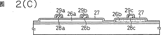
其后,使硅膜构图,以形成岛状区域26a(外围驱动电路区域)和26b(阵列象素电路区域)。作为TFTs的栅绝缘膜,由四乙氧硅烷[四乙基原硅酸盐,Si(OC2H5)4]和氧形成厚度为1000的硅氧化膜27。还将三氯乙烯(C2HCl3)加到原料气体中。在该膜成形之前,把流量为400SCCM的氧送入腔室。在衬底温度为300℃,总压力5Pa,以及RF功率为150W下产生等离子。这种条件保持10分钟。接着分别以300SCCM,15SCCM和2SCCM的流量把氧,四乙基原硅酸盐和三氯乙烯导入腔室。这样就形成硅氧化膜,而衬底的温度是300℃,RF功率为75W,总压为为5Pa。膜制成后,在100torr的压力下把氢输入腔室。在350℃温度下,将该叠层制品退火35分钟。
接着,用溅射法淀积厚度6000~8000如6000的含2%硅的铝作为铝膜。还可用钽、钨、钛或钼替代铝。最好连续执行形成硅氧化膜27的步骤和形成铝膜的步骤。将铝膜刻成图形,以形成TFTs的栅电极28a、28b和28c。将铝互连线的表面作阳极氧化,在表面形成氧化层29a、29b和29c。在酒石酸的1~5%乙二醇溶液内实施阳极氧化处理。所获得氧化层的厚度为2000(图2(C))。
然后利用等离子掺杂法,把杂质或磷注入到硅区域。利用磷化氢(PH3)作为气体掺杂剂,加速电压为60~90KV例如80KV。剂量为1×10¹⁵~8×10¹⁵/cm2。这样就形成N型掺杂区域30a。用光刻胶掩蔽左边的TFT(N沟道TFT),再用等离子掺杂法把杂质或硼注入到右边的外围电路区域TFT的硅区域,以及注入构成阵列电路TFTs的硅区域。利用乙硼烷(B2H6)作为气体掺杂剂加速电压为50~80KV例如65KV,剂量为1×1015~8×1015/cm2例如5×1015/cm2例如5×1015/cm2,上述剂量要大于先前注入磷的剂量。这样就形成了P型掺杂区和30c。
然后,用激光退火激活杂质。用作激光照射的有波长为248nm和脉冲持续时间20nsec的KrF准分子激光器发射的光。激光能量密度为200~400mJ/cm2例如250mJ/cm2。对每个位置照射激光2~10次例如两次(图2(D))。
接着,通过等离子CVD,用四乙基原硅酸盐(TEOS)形成厚度2000°A的硅氧化膜31作为层间绝缘体。利用溅射法,淀积500~1000例如800厚的铟锡氧化物(ITO)作为铟锡氧氧化膜。刻蚀该膜,形成象素电极32。在层间绝缘体31内形成接触孔。由金属材料例如氮化钛和铝的多层膜形成源、漏电极、用于外围驱动电路的TFTs的导电互连线33a、33b、33c和各电极以及用于阵列象素电路的TFTs的导电互连线33d、33e。这样就完成了半导体电路(图2(E))。
制造半导体电路的外围驱动电路TFTs的性能决不劣于用已有技术激光结晶制作的TFTs性能。利用按照本实施例的这些TFTs构成移位寄存器。我们已经征实:用15V漏电压,该移位寄存器能在11MHz下工作,用17V漏电压,则能在16MHz下工作。并且在可靠性测试中,没有看出新型TFTs和由公知技术方法制造的TFTs之间存在差异。就在阵列区域象素电路内的TFTs的性能而论,漏电流小于10-13A。
实施例3
图4(A)~4(E)是半导体电路的横向剖面图,诸图说明制造按照本实施例电路的各连续执行步骤。首先,在由Corning7059制成的衬底上溅射厚度2000°A的氧化硅,作为底层11。利用等离子CVD在基层11上形成厚度为500~1500例如500的本征(I)型非晶硅膜12。然后,立即用溅射法,有选择性地形成含浓度为1×10¹⁸/cm3的镍并用厚度为5~200例如50的硅膜13如所示。利用剥离(lift-off)工艺制作这镍膜13。还可使用旋涂法代替溅射法(图4(A))。
用激光照射非晶硅膜12的整个表面,使其结晶化。就这种激光照射而言,可使用波长为248nm和脉冲持续时间为20nsec的KrF准分子激光器发射的光。
也可用其他激光器如波长为353nm的XeF准分子激光器,波长为308nm的XeCl准分子激光器,波长为193nm的ArF准发子激光器和其他激光器。激光的能量密度为200~500mJ/cm2,例如350mJ/cm2。向每个位置发射激光2~10次,例如2次。在激光照射期间,衬底被加热到100~450℃,例如300℃。结果,使非晶硅膜的整个表面结晶化。然而,位于硅镍膜13下面的硅膜12a那些部位的结晶度要优于在其他区域内硅膜12b的结晶度,这是因为镍促进了结晶化(图4(B))。
将硅膜光刻成图形,以形成岛状硅区域14a(外围驱动电路区域)和14b(阵列区域)。用溅射法,淀积1000厚的硅氧化物作为栅绝缘膜15。在溅射工艺中,使用含氧化硅的靶子。在该工艺过程中,衬底的温度为200~400℃,例如350℃。溅射的气氛环境含氧和氩。氩与氧的比率在0和0.5之间,例如小于0.1。接着,通过LPCVD法,形成厚为3000~8000,例如6000以及含0.1~2%磷的硅膜。最好,连续实施形成硅氧化膜15的步骤和形成硅膜的步骤。再将硅膜刻成图形,以形成栅电极16a、16b和16C(图4(C))。
于是,利用栅电极作为掩模,用等离子掺杂法,把杂质或磷和硼注入硅区域。磷化氢(PH3)和乙硼烷(B2H6)都可用作掺杂剂气体。使用磷化氢时,加速电压为60~90KV,例如80KV;使用乙硼烷时,加速电压为40~80KV,例如65KV。剂量为1×10¹⁵~8×10¹⁵/cm2。例如磷剂量为2×1015/cm2;硼的剂量为5×1015/cm2,结果,形成了N型掺杂区域17a,P型掺杂区域17b、17c。
此后,由激光退火激活杂质。就该激光退火而言,使用波长为248nm和脉冲持续时间20nsec的KrF准分子激光器发射的光。其他激光器如XeF准分子激光器发射的波长为353nm的光、XeCl准分子激光器发射的波长为308nm的光、ArF准分子激光器发射的波长为193nm的光以及其它的激光器的光。激光的能量密度为200~400mJ/cm2例如250mJ/cm2向每个位置照射激光2~10次,例如2次。在激光退火期间,衬底被加热到100~450℃,例如250℃。这样就激活了掺杂区域17a~17c(图4D)。
然后,用等离子CVD法,形成厚度为6000的硅氧化膜18作为层内绝缘体。通过溅射形成厚度为500~1000例如800的铟锡氧化物膜(ITO)。将该膜刻成图形,形成象素电极19。再在层间绝缘体内形成接触孔。用金属材料例如氮化钛和铝的多层膜制作电极,外围驱动电路的TFTs的导电互连线20a、20b、20c和电极,以及阵列象素电路的TFTs的导电互连线20d、20e和电极。最后在350℃、1个大气压下以及氢环境中经30分钟,使叠层制品退火。这样,就完成了半导体电路(图4(E))。
用SIMS来测试定本实施例所获得TFTs有源区域内所含镍的浓度,外围驱动电路内TFTs中的镍浓度为1×10¹⁷~5×10¹⁷/cm3。象素电路内TFTs中的镍浓度低于检测下限,这个下限为1×1016/cm3。
实施例4
图5(A)~5(E)是半导体器件的横剖面图。诸图说明连续进行制造按照本实施例的器件的各个步骤。利用溅射在由Corn-ing7059制成的衬底21上,形成厚度2000的硅氧化膜22。然后,用等离子CVD法,在硅氧化膜22上形成厚度为200~1500例如500的非晶硅膜23。在用光刻胶24掩蔽该膜同时,用离子注入法,有选择性地把镍离子注入到非晶硅膜23内。这样,形成浓度为1×10¹⁵~1×10¹⁸/cm3例如5×1018/cm3的含镍区域25。这些区域25的深度是200~500。根据这个深度确定加速电压。由于本实施例采用离子注入法,在控制镍浓度方面比起实施例3的技术就更加有效(图5(A))。然后,在350~650℃,最好是400~550℃例如500℃,在氮气氛中使衬底退火2小时。作为结果,镍掺杂区域的晶化过程初步得到推进,而后,用激光照射非晶硅膜23的整个表面,使这些区域晶化。就该激光照射来说,使用波长248nm和脉冲持续时间20nsec的KrF准分子激光器发射的光。激光的能量密度为200~500mJ/cm2例如350mJ/cm2。向每个位置发射激光2~10,例如2次。在激光照射期间,衬底加热到100~450℃例如350℃。结果,硅膜晶化。用镍掺杂硅膜的那些区域23a在结晶度方面要优于未掺杂区域23b(图5(B))。
其后,使硅膜刻成图形,形成岛状硅区域26a(外围驱动电路区域)和26b(阵列象素电路区域)。用等离子CVD法,形成厚度1000的硅氧化膜27作为TFTs的栅绝缘膜,上述过程使用四乙氧硅烷(四乙基原硅酸盐Si(OC2H5)4)和氧作为气体原料。三氯乙烯(C2HCl3)被加到气体原料中。在膜成形前,以400SCCM的流量把氧送入腔室内。在衬底温度为300℃,总压力为5Pa,RF功率为150W条件下产生等离子。接着,分别以300SCCM、15SCCM和2SCCM的流量把氧、四乙基原硅酸盐和三氯乙烯导入腔室。这样就形成硅氧化膜。衬底的温度为300℃,RF功率为75W,总压力为5Pa。做成膜后,把氢导入在100torr压力下腔室。再在350℃下经35分钟使叠层制品退火。
然后,用溅射法淀积厚度为6000~8000,例如6000的含2%硅的铝。也可用钽、钨、钛或钼代替铝。最好是连续实施形成硅氧化膜27的步骤和形成铝膜的步骤。将铝膜刻成图形,形成TFTs栅电极28a、28b和28c。使铝互连线表面阳极氧化,以在表面形成氧化层29a、29b和29c。在酒石酸的1~5%乙二醇溶液内进行阳极氧化处理。所获得氧化层厚度为2000(图5C)。
用等离子掺杂法,把杂质,或磷注入硅区域。用磷氢(PH3)作为气体掺杂剂。加速电压为60~90KV,例如80KV。剂量为1×10¹⁵~8×10¹⁵/cm2例如2×1015/cm2。这样就形成N型掺杂区域30a。由光刻胶掩蔽左边的TFT(N沟道TFT),再次利用等离子掺杂法,把杂质,或硼注入右边的外围电路区域TFT的硅区域和形成阵列电路TFTs的硅区域。把乙硼烷(B2H6)用作气体掺杂剂。加速电压为50~80KV,例如65KV。剂量为1×1015~8×1015/cm2,例如5×1015/cm2,该剂量要大于在该注入磷的剂量。就用该方法,形成P型掺杂区域30b和30c。
此后,由激光退火激活杂质。就这激光退火来说,可使用波长248nm及脉冲持续时间20nsec的KrF准分子激光器发射的光。激光的能量密度为200~400mJ/cm2,例如250mJ/cm2。向每个位置发射激光2~10次,例如2次(图2(D))。
然后,通过等离子CVD法,由四乙基原硅酸盐形成厚度为2000的硅氧化膜31作为层间绝缘体。通过溅射,形成厚度为500~1000,例如800的铟锡氧化物膜(ITO)。将该膜刻成图形,形成象素电极32。然后,在层间绝缘体31内形成接触孔。由金属材料,如氮化钛和铝的多层膜制作外围驱动电路的TFTs电极和电互连线33a、33b、33c,以及阵列象素电路的TFTs的电极和导电互连线33d、33e。这样,就完成了半导体电路(图5(E))。
所制成的半导体电路的外围驱动电路的TFTs的性能决不低于由公知的激光晶化技术制造的TFTs的性能。利用按照本实施例的这些TFTs构成移位寄存器。我们已经确认:用15V漏电压,移位寄存器能在11MHz下工作,用17V漏电压,则移位寄存器能在16MHz下工作。还有,在可靠性测试中,没有观测到新型TFTs和由公知技术方法制作的TFTs之间的差异。就阵列区域(象素电路)内TFTs的性能来说,漏电流小于10-13A。
如上述实施例所述,本发明在同样的衬底上可制作能高速工作的TFTs和显示出低漏电流的TFTs。该结构可应用于液晶显示器,易于大批量生产TFTs,而且性能得到改善。当然,在衬底上也可制作仅仅展示这两个特征之一的TFTs。
此外,在本发明中还可以低温,如500℃,和短时,如4小时使硅晶化,而改善生产率。采用高于600℃进行的传统工艺,会使玻璃衬底缩变,扭曲,导致生产成品率下降。而采用本发明使这个问题完全得到解决。这还意味着:用一次操作中处理具有很大面积的衬底。尤其是,通过把大面积的衬底切成许多半导体电路,比如阵列电路,这样可极大地降低每个电路的价格。这样一来,本发明对工业上更有利。
Claims (27)
1.一种制造半导体电路的方法,包括:
在一衬底的绝缘表面上面形成含硅的半导体膜,该半导体膜具有第一部分、第二部分及一表面;
选择性地将至少一种催化元素只引入所述半导体膜的所述第一部分,所述至少一种催化元素用以促进该半导体膜的晶化;和
用光照射所述半导体膜的所述表面从而促进所述半导体膜的晶化,
其中,所述半导体膜的结晶性在所述第一部分比在所述第二部分更强。
2.如权利要求1所述的制造半导体电路的方法,其中,所述至少一种催化元素包括镍、铁、钴和铂构成的一组中的至少其中之一。
3.如权利要求1所述的制造半导体电路的方法,其中,所述光为激光或强度等于激光的光。
4.一种生产有源阵列型半导体电路的方法,所述电路至少包括第一组薄膜晶体管和第二组薄膜晶体管,第一组薄膜晶体管形成在一衬底的第一部分上面,构成一个有源阵列电路,第二组薄膜晶体管形成在该衬底的第二部分上面,构成驱动所述有源阵列电路的外围电路,所述方法包括:
在所述衬底的上面形成非晶硅膜;
将一种催化材料只引入所述第二部分的上面的所述非晶硅膜的一部分之内或之上,所述催化材料用以促进该硅膜的晶化;
用光照射所述衬底的所述第一部分和第二部分上面的所述非晶硅膜,以使所述非晶硅膜晶化;和
将所述硅膜刻成多个硅岛的图形,从而构成所述第一组薄膜晶体管和所述第二组薄膜晶体管。
5.如权利要求4所述的生产半导体电路的方法,其中还包括:
用所述光照射所述非晶硅膜之前对所述非晶硅膜加热使其退火,以使所述非晶硅膜进行晶化。
6.如权利要求5所述的生产半导体电路的方法,其中,所述非晶硅膜的加热退火是在400-500℃温度范围内进行的。
7.如权利要求4所述的生产半导体电路的方法,其中,所述催化材料是通过将其放置到与所述非晶硅膜接触的方法而加入的。
8.如权利要求4所述的生产半导体电路的方法,其中,所述催化材料是通过离子注入法加入的。
9.如权利要求4所述的生产半导体电路的方法,其中,使所述非晶硅膜晶化以后,在所述硅膜中所含的所述催化元素的浓度不超过1×10²⁰原子/cm3。
10.如权利要求1所述的制造半导体电路的方法,其中,在所述晶化以后在所述半导体膜中所含的所述催化元素的浓度不超过1×10²⁰原子/cm3。
11.一种制造半导体电路的方法,包括:
在一衬底上面形成含硅的半导体膜,所述膜具有一个表面;
使至少一种催化元素与所述半导体膜的所有所述表面相接触,以促进该半导体膜的晶化;
用光选择性地照射所述半导体膜的除第二部分外的第一部分,以使该半导体膜的所述第一部分晶化;和
在所述照射步骤之后,通过加热使所述半导体膜退火,以晶化所述半导体膜的至少所述第二部分。
12.如权利要求11所述的方法,其中,所述催化元素包括镍、铁、钴和铂的至少其中之一。
13.如权利要求11所述的方法,其中,所述退火步骤是在580℃或以下的温度进行的。
14.如权利要求11所述的方法,其中,所述光为激光或强度等于激光的光。
15.一种制造半导体电路的方法,包括:
在一衬底上面形成含硅的半导体膜;
将至少一种催化元素引入所述半导体膜内,以促进该半导体膜的晶化;
用光选择性地照射所述半导体膜的除第二部分外的所述半导体膜的第一部分,以使该半导体膜的所述第一部分晶化;和
在用光照射所述第一部分之后,通过加热使所述半导体膜退火,以晶化所述半导体膜的至少所述第二部分。
16.如权利要求15所述的制造半导体电路的方法,其中,在所述引入步骤中,所述半导体膜中的所述至少一种催化元素的最低浓度值,按SIMS测量,超过1×10¹⁶/cm3。
17.如权利要求15所述的制造半导体电路的方法,其中,所述半导体膜的退火是在580℃或以下的温度进行的。
18.如权利要求15所述的制造半导体电路的方法,其中,所述光为激光或强度等于激光的光。
19.如权利要求15所述的制造半导体电路的方法,其中,在所述半导体膜的第一部分晶化以后,所述半导体膜中所含的所述催化元素的浓度不超过1×10²⁰原子/cm3。
20.一种制造有源阵列型半导体电路的方法,所述电路至少包括第一组薄膜晶体管和第二组薄膜晶体管,第一组薄膜晶体管形成在一衬底的第一部分的上面,构成一个有源阵列电路,第二组薄膜晶体管形成在该衬底的第二部分的上面,构成驱动所述有源阵列电路的外围电路,所述方法包括:
在所述衬底的上面形成非晶硅膜;
将一种催化材料引入位于所述衬底的第一部分和第二部分两者上面的所述非晶硅膜之内或之上,用以促进该硅膜的晶化;
用光只照射位于所述衬底的第二部分上面的所述非晶硅膜部分,以使该部分晶化;和
将所述硅膜刻成多个硅岛的图形,以构成所述第一组薄膜晶体管和所述第二组薄膜晶体管。
21.如权利要求20所述的制造半导体电路的方法,其中还包括:
通过加热使位于所述衬底的所述第一部分上的所述硅膜进行退火。
22.如权利要求20所述的制造半导体电路的方法,其中,所述催化材料选自镍、铁、钴和铂组成的组。
23.如权利要求20所述的制造半导体电路的方法,其中,所述催化材料是通过使其设置为与所述非晶硅膜接触的方式而引入的。
24.如权利要求20所述的制造半导体电路的方法,其中,所述催化材料是通过离子注入法而引入的。
25.如权利要求1所述的制造半导体电路的方法,其中,所述催化元素被形成为只与所述半导体膜的第一部分接触。
26.如权利要求15所述的制造半导体电路的方法,其中,所述催化元素是通过离子注入法而引入的。
27.如权利要求1所述的制造半导体电路的方法,其中,所述半导体膜的整个表面用光照射。
Applications Claiming Priority (6)
| Application Number | Priority Date | Filing Date | Title |
|---|---|---|---|
| JP79004/93 | 1993-03-12 | ||
| JP79005/1993 | 1993-03-12 | ||
| JP79004/1993 | 1993-03-12 | ||
| JP7900493A JP3359690B2 (ja) | 1993-03-12 | 1993-03-12 | 半導体回路の作製方法 |
| JP79005/93 | 1993-03-12 | ||
| JP7900593 | 1993-03-12 |
Related Parent Applications (1)
| Application Number | Title | Priority Date | Filing Date |
|---|---|---|---|
| CN94104267A Division CN1092844C (zh) | 1993-03-12 | 1994-03-12 | 制造半导体器件的方法 |
Publications (2)
| Publication Number | Publication Date |
|---|---|
| CN1328340A CN1328340A (zh) | 2001-12-26 |
| CN1305107C true CN1305107C (zh) | 2007-03-14 |
Family
ID=26420092
Family Applications (4)
| Application Number | Title | Priority Date | Filing Date |
|---|---|---|---|
| CNB991267273A Expired - Lifetime CN1157759C (zh) | 1993-03-12 | 1994-03-12 | 制造半导体器件的方法 |
| CNB011166339A Expired - Fee Related CN1305107C (zh) | 1993-03-12 | 1994-03-12 | 半导体电路的制造方法 |
| CN94104267A Expired - Fee Related CN1092844C (zh) | 1993-03-12 | 1994-03-12 | 制造半导体器件的方法 |
| CNB991103912A Expired - Lifetime CN1136612C (zh) | 1993-03-12 | 1999-07-16 | 半导体电路及半导体器件 |
Family Applications Before (1)
| Application Number | Title | Priority Date | Filing Date |
|---|---|---|---|
| CNB991267273A Expired - Lifetime CN1157759C (zh) | 1993-03-12 | 1994-03-12 | 制造半导体器件的方法 |
Family Applications After (2)
| Application Number | Title | Priority Date | Filing Date |
|---|---|---|---|
| CN94104267A Expired - Fee Related CN1092844C (zh) | 1993-03-12 | 1994-03-12 | 制造半导体器件的方法 |
| CNB991103912A Expired - Lifetime CN1136612C (zh) | 1993-03-12 | 1999-07-16 | 半导体电路及半导体器件 |
Country Status (4)
| Country | Link |
|---|---|
| US (4) | US5569610A (zh) |
| KR (1) | KR0171437B1 (zh) |
| CN (4) | CN1157759C (zh) |
| TW (1) | TW241377B (zh) |
Families Citing this family (202)
| Publication number | Priority date | Publication date | Assignee | Title |
|---|---|---|---|---|
| US6975296B1 (en) * | 1991-06-14 | 2005-12-13 | Semiconductor Energy Laboratory Co., Ltd. | Electro-optical device and method of driving the same |
| CN1052569C (zh) * | 1992-08-27 | 2000-05-17 | 株式会社半导体能源研究所 | 制造半导体器件的方法 |
| US6323071B1 (en) | 1992-12-04 | 2001-11-27 | Semiconductor Energy Laboratory Co., Ltd. | Method for forming a semiconductor device |
| TW226478B (en) * | 1992-12-04 | 1994-07-11 | Semiconductor Energy Res Co Ltd | Semiconductor device and method for manufacturing the same |
| US5403762A (en) * | 1993-06-30 | 1995-04-04 | Semiconductor Energy Laboratory Co., Ltd. | Method of fabricating a TFT |
| US6997985B1 (en) | 1993-02-15 | 2006-02-14 | Semiconductor Energy Laboratory Co., Ltd. | Semiconductor, semiconductor device, and method for fabricating the same |
| JP3562588B2 (ja) * | 1993-02-15 | 2004-09-08 | 株式会社半導体エネルギー研究所 | 半導体装置の製造方法 |
| EP1119053B1 (en) * | 1993-02-15 | 2011-11-02 | Semiconductor Energy Laboratory Co., Ltd. | Method for fabricating TFT semiconductor device |
| TW241377B (zh) | 1993-03-12 | 1995-02-21 | Semiconductor Energy Res Co Ltd | |
| US6413805B1 (en) | 1993-03-12 | 2002-07-02 | Semiconductor Energy Laboratory Co., Ltd. | Semiconductor device forming method |
| JP3535205B2 (ja) * | 1993-03-22 | 2004-06-07 | 株式会社半導体エネルギー研究所 | 薄膜トランジスタの作製方法 |
| US5818076A (en) * | 1993-05-26 | 1998-10-06 | Semiconductor Energy Laboratory Co., Ltd. | Transistor and semiconductor device |
| US6090646A (en) * | 1993-05-26 | 2000-07-18 | Semiconductor Energy Laboratory Co., Ltd. | Method for producing semiconductor device |
| KR100186886B1 (ko) * | 1993-05-26 | 1999-04-15 | 야마자끼 승페이 | 반도체장치 제작방법 |
| KR100355938B1 (ko) * | 1993-05-26 | 2002-12-16 | 가부시키가이샤 한도오따이 에네루기 켄큐쇼 | 반도체장치제작방법 |
| JPH06349735A (ja) * | 1993-06-12 | 1994-12-22 | Semiconductor Energy Lab Co Ltd | 半導体装置 |
| US6713330B1 (en) | 1993-06-22 | 2004-03-30 | Semiconductor Energy Laboratory Co., Ltd. | Method of fabricating a thin film transistor |
| US5488000A (en) | 1993-06-22 | 1996-01-30 | Semiconductor Energy Laboratory Co., Ltd. | Method of fabricating a thin film transistor using a nickel silicide layer to promote crystallization of the amorphous silicon layer |
| US5663077A (en) | 1993-07-27 | 1997-09-02 | Semiconductor Energy Laboratory Co., Ltd. | Method of manufacturing a thin film transistor in which the gate insulator comprises two oxide films |
| JP2814049B2 (ja) | 1993-08-27 | 1998-10-22 | 株式会社半導体エネルギー研究所 | 半導体装置およびその作製方法 |
| JP3030368B2 (ja) | 1993-10-01 | 2000-04-10 | 株式会社半導体エネルギー研究所 | 半導体装置およびその作製方法 |
| US6777763B1 (en) * | 1993-10-01 | 2004-08-17 | Semiconductor Energy Laboratory Co., Ltd. | Semiconductor device and method for fabricating the same |
| US6798023B1 (en) | 1993-12-02 | 2004-09-28 | Semiconductor Energy Laboratory Co., Ltd. | Semiconductor device comprising first insulating film, second insulating film comprising organic resin on the first insulating film, and pixel electrode over the second insulating film |
| US5869362A (en) * | 1993-12-02 | 1999-02-09 | Semiconductor Energy Laboratory Co., Ltd. | Method of manufacturing semiconductor device |
| CN1156918C (zh) | 1993-12-02 | 2004-07-07 | 株式会社半导体能源研究所 | 半导体器件 |
| TW272319B (zh) * | 1993-12-20 | 1996-03-11 | Sharp Kk | |
| KR100319332B1 (ko) | 1993-12-22 | 2002-04-22 | 야마자끼 순페이 | 반도체장치및전자광학장치 |
| JP3221473B2 (ja) | 1994-02-03 | 2001-10-22 | 株式会社半導体エネルギー研究所 | 半導体装置の作製方法 |
| JP3195157B2 (ja) * | 1994-03-28 | 2001-08-06 | シャープ株式会社 | 半導体装置の製造方法およびその製造装置 |
| US6059873A (en) * | 1994-05-30 | 2000-05-09 | Semiconductor Energy Laboratory Co., Ltd. | Optical processing method with control of the illumination energy of laser light |
| US5650636A (en) * | 1994-06-02 | 1997-07-22 | Semiconductor Energy Laboratory Co., Ltd. | Active matrix display and electrooptical device |
| JP3067949B2 (ja) * | 1994-06-15 | 2000-07-24 | シャープ株式会社 | 電子装置および液晶表示装置 |
| TW273639B (en) * | 1994-07-01 | 1996-04-01 | Handotai Energy Kenkyusho Kk | Method for producing semiconductor device |
| TW280943B (zh) * | 1994-07-15 | 1996-07-11 | Sharp Kk | |
| TW345705B (en) | 1994-07-28 | 1998-11-21 | Handotai Energy Kenkyusho Kk | Laser processing method |
| JP3072005B2 (ja) * | 1994-08-25 | 2000-07-31 | シャープ株式会社 | 半導体装置及びその製造方法 |
| JPH0869967A (ja) | 1994-08-26 | 1996-03-12 | Semiconductor Energy Lab Co Ltd | 半導体装置の作製方法 |
| TW403993B (en) * | 1994-08-29 | 2000-09-01 | Semiconductor Energy Lab | Semiconductor circuit for electro-optical device and method of manufacturing the same |
| JP3442500B2 (ja) | 1994-08-31 | 2003-09-02 | 株式会社半導体エネルギー研究所 | 半導体回路の作製方法 |
| TW374247B (en) * | 1994-09-15 | 1999-11-11 | Semiconductor Energy Lab Co Ltd | Method of fabricating semiconductor device |
| US5712191A (en) * | 1994-09-16 | 1998-01-27 | Semiconductor Energy Laboratory Co., Ltd. | Method for producing semiconductor device |
| US6242289B1 (en) | 1995-09-08 | 2001-06-05 | Semiconductor Energy Laboratories Co., Ltd. | Method for producing semiconductor device |
| US5818068A (en) * | 1994-09-22 | 1998-10-06 | Sharp Kabushiki Kaisha | Thin film transistor circuit and an active matrix type display device |
| USRE43450E1 (en) | 1994-09-29 | 2012-06-05 | Semiconductor Energy Laboratory Co., Ltd. | Method for fabricating semiconductor thin film |
| US5915174A (en) * | 1994-09-30 | 1999-06-22 | Semiconductor Energy Laboratory Co., Ltd. | Semiconductor device and method for producing the same |
| US6300659B1 (en) | 1994-09-30 | 2001-10-09 | Semiconductor Energy Laboratory Co., Ltd. | Thin-film transistor and fabrication method for same |
| US5942768A (en) * | 1994-10-07 | 1999-08-24 | Semionductor Energy Laboratory Co., Ltd. | Semiconductor device having improved crystal orientation |
| US6008101A (en) * | 1994-11-29 | 1999-12-28 | Semiconductor Energy Laboratory Co., Ltd. | Laser processing method of semiconductor device |
| US5756364A (en) * | 1994-11-29 | 1998-05-26 | Semiconductor Energy Laboratory Co., Ltd. | Laser processing method of semiconductor device using a catalyst |
| US6337229B1 (en) | 1994-12-16 | 2002-01-08 | Semiconductor Energy Laboratory Co., Ltd. | Method of making crystal silicon semiconductor and thin film transistor |
| JP2900229B2 (ja) | 1994-12-27 | 1999-06-02 | 株式会社半導体エネルギー研究所 | 半導体装置およびその作製方法および電気光学装置 |
| US6331475B1 (en) | 1995-01-12 | 2001-12-18 | Semiconductor Energy Laboratory Co., Ltd. | Method and manufacturing semiconductor device |
| US5929464A (en) * | 1995-01-20 | 1999-07-27 | Semiconductor Energy Laboratory Co., Ltd. | Active matrix electro-optical device |
| JP4130237B2 (ja) * | 1995-01-28 | 2008-08-06 | 株式会社半導体エネルギー研究所 | 結晶性珪素膜の作製方法及び半導体装置の作製方法 |
| TW305063B (zh) | 1995-02-02 | 1997-05-11 | Handotai Energy Kenkyusho Kk | |
| JP3364081B2 (ja) * | 1995-02-16 | 2003-01-08 | 株式会社半導体エネルギー研究所 | 半導体装置の作製方法 |
| JP3778456B2 (ja) * | 1995-02-21 | 2006-05-24 | 株式会社半導体エネルギー研究所 | 絶縁ゲイト型薄膜半導体装置の作製方法 |
| US5757456A (en) * | 1995-03-10 | 1998-05-26 | Semiconductor Energy Laboratory Co., Ltd. | Display device and method of fabricating involving peeling circuits from one substrate and mounting on other |
| JP3138169B2 (ja) * | 1995-03-13 | 2001-02-26 | シャープ株式会社 | 半導体装置の製造方法 |
| US5834327A (en) | 1995-03-18 | 1998-11-10 | Semiconductor Energy Laboratory Co., Ltd. | Method for producing display device |
| US7075002B1 (en) | 1995-03-27 | 2006-07-11 | Semiconductor Energy Laboratory Company, Ltd. | Thin-film photoelectric conversion device and a method of manufacturing the same |
| KR100265179B1 (ko) * | 1995-03-27 | 2000-09-15 | 야마자끼 순페이 | 반도체장치와 그의 제작방법 |
| TW383502B (en) | 1995-06-01 | 2000-03-01 | Seniconductor Energy Lab Kk | Method of manufacturing semiconductor device |
| US6337109B1 (en) * | 1995-06-07 | 2002-01-08 | Semiconductor Energy Laboratory Co., Ltd. | Method of producing crystalline semiconductor |
| JP4056571B2 (ja) | 1995-08-02 | 2008-03-05 | 株式会社半導体エネルギー研究所 | 半導体装置の作製方法 |
| JP3295679B2 (ja) * | 1995-08-04 | 2002-06-24 | 株式会社半導体エネルギー研究所 | 半導体装置の作製方法 |
| JPH0951035A (ja) * | 1995-08-07 | 1997-02-18 | Mitsubishi Electric Corp | 層間絶縁膜の形成方法 |
| JP3917205B2 (ja) * | 1995-11-30 | 2007-05-23 | 株式会社半導体エネルギー研究所 | 半導体装置の作製方法 |
| JP3907726B2 (ja) | 1995-12-09 | 2007-04-18 | 株式会社半導体エネルギー研究所 | 微結晶シリコン膜の作製方法、半導体装置の作製方法及び光電変換装置の作製方法 |
| JP3124480B2 (ja) * | 1995-12-12 | 2001-01-15 | 株式会社半導体エネルギー研究所 | 半導体装置の作製方法 |
| US6204101B1 (en) | 1995-12-15 | 2001-03-20 | Semiconductor Energy Laboratory Co., Ltd. | Method of manufacturing semiconductor device |
| TW319912B (zh) * | 1995-12-15 | 1997-11-11 | Handotai Energy Kenkyusho Kk | |
| JP3729955B2 (ja) | 1996-01-19 | 2005-12-21 | 株式会社半導体エネルギー研究所 | 半導体装置の作製方法 |
| US5985740A (en) * | 1996-01-19 | 1999-11-16 | Semiconductor Energy Laboratory Co., Ltd. | Method of manufacturing a semiconductor device including reduction of a catalyst |
| JP3645380B2 (ja) | 1996-01-19 | 2005-05-11 | 株式会社半導体エネルギー研究所 | 半導体装置の作製方法、情報端末、ヘッドマウントディスプレイ、ナビゲーションシステム、携帯電話、ビデオカメラ、投射型表示装置 |
| JP3645378B2 (ja) * | 1996-01-19 | 2005-05-11 | 株式会社半導体エネルギー研究所 | 半導体装置の作製方法 |
| US6478263B1 (en) | 1997-01-17 | 2002-11-12 | Semiconductor Energy Laboratory Co., Ltd. | Semiconductor device and its manufacturing method |
| JP3645379B2 (ja) | 1996-01-19 | 2005-05-11 | 株式会社半導体エネルギー研究所 | 半導体装置の作製方法 |
| US5888858A (en) * | 1996-01-20 | 1999-03-30 | Semiconductor Energy Laboratory Co., Ltd. | Semiconductor device and fabrication method thereof |
| US7056381B1 (en) | 1996-01-26 | 2006-06-06 | Semiconductor Energy Laboratory Co., Ltd. | Fabrication method of semiconductor device |
| US6180439B1 (en) | 1996-01-26 | 2001-01-30 | Semiconductor Energy Laboratory Co., Ltd. | Method for fabricating a semiconductor device |
| US6465287B1 (en) * | 1996-01-27 | 2002-10-15 | Semiconductor Energy Laboratory Co., Ltd. | Method for fabricating a semiconductor device using a metal catalyst and high temperature crystallization |
| US6063654A (en) * | 1996-02-20 | 2000-05-16 | Semiconductor Energy Laboratory Co., Ltd. | Method of manufacturing a thin film transistor involving laser treatment |
| TW335503B (en) | 1996-02-23 | 1998-07-01 | Semiconductor Energy Lab Kk | Semiconductor thin film and manufacturing method and semiconductor device and its manufacturing method |
| TW374196B (en) | 1996-02-23 | 1999-11-11 | Semiconductor Energy Lab Co Ltd | Semiconductor thin film and method for manufacturing the same and semiconductor device and method for manufacturing the same |
| TW317643B (zh) * | 1996-02-23 | 1997-10-11 | Handotai Energy Kenkyusho Kk | |
| JP3472024B2 (ja) | 1996-02-26 | 2003-12-02 | 株式会社半導体エネルギー研究所 | 半導体装置の作製方法 |
| US6100562A (en) | 1996-03-17 | 2000-08-08 | Semiconductor Energy Laboratory Co., Ltd. | Method of manufacturing a semiconductor device |
| US6133119A (en) * | 1996-07-08 | 2000-10-17 | Semiconductor Energy Laboratory Co., Ltd. | Photoelectric conversion device and method manufacturing same |
| US5773329A (en) * | 1996-07-24 | 1998-06-30 | International Business Machines Corporation | Polysilicon grown by pulsed rapid thermal annealing |
| JPH10199807A (ja) | 1996-12-27 | 1998-07-31 | Semiconductor Energy Lab Co Ltd | 結晶性珪素膜の作製方法 |
| TW386238B (en) | 1997-01-20 | 2000-04-01 | Semiconductor Energy Lab | Semiconductor device and method of manufacturing the same |
| JPH10214974A (ja) * | 1997-01-28 | 1998-08-11 | Semiconductor Energy Lab Co Ltd | 半導体装置およびその作製方法 |
| US6830616B1 (en) * | 1997-02-10 | 2004-12-14 | Semiconductor Energy Laboratory Co., Ltd. | Manufacturing method of semiconductor and manufacturing method of semiconductor device |
| JP4242461B2 (ja) | 1997-02-24 | 2009-03-25 | 株式会社半導体エネルギー研究所 | 半導体装置の作製方法 |
| JP3544280B2 (ja) | 1997-03-27 | 2004-07-21 | 株式会社半導体エネルギー研究所 | 半導体装置の作製方法 |
| JPH10282414A (ja) * | 1997-04-09 | 1998-10-23 | Canon Inc | ズームレンズ |
| US6541793B2 (en) | 1997-05-30 | 2003-04-01 | Semiconductor Energy Laboratory Co., Ltd. | Thin-film transistor and semiconductor device using thin-film transistors |
| JP3376247B2 (ja) * | 1997-05-30 | 2003-02-10 | 株式会社半導体エネルギー研究所 | 薄膜トランジスタ及び薄膜トランジスタを用いた半導体装置 |
| US6307214B1 (en) | 1997-06-06 | 2001-10-23 | Semiconductor Energy Laboratory Co., Ltd. | Semiconductor thin film and semiconductor device |
| JP3844561B2 (ja) | 1997-06-10 | 2006-11-15 | 株式会社半導体エネルギー研究所 | 半導体装置の作製方法 |
| US6501094B1 (en) * | 1997-06-11 | 2002-12-31 | Semiconductor Energy Laboratory Co., Ltd. | Semiconductor device comprising a bottom gate type thin film transistor |
| JP3717634B2 (ja) | 1997-06-17 | 2005-11-16 | 株式会社半導体エネルギー研究所 | 半導体装置の作製方法 |
| JP3295346B2 (ja) | 1997-07-14 | 2002-06-24 | 株式会社半導体エネルギー研究所 | 結晶性珪素膜の作製方法及びそれを用いた薄膜トランジスタ |
| JP3830623B2 (ja) * | 1997-07-14 | 2006-10-04 | 株式会社半導体エネルギー研究所 | 結晶性半導体膜の作製方法 |
| US6326226B1 (en) | 1997-07-15 | 2001-12-04 | Lg. Philips Lcd Co., Ltd. | Method of crystallizing an amorphous film |
| US5940693A (en) * | 1997-07-15 | 1999-08-17 | Sharp Laboratories Of America, Inc. | Selective silicide thin-film transistor and method for same |
| JPH1140498A (ja) | 1997-07-22 | 1999-02-12 | Semiconductor Energy Lab Co Ltd | 半導体装置の作製方法 |
| JP3939399B2 (ja) * | 1997-07-22 | 2007-07-04 | 株式会社半導体エネルギー研究所 | 半導体装置の作製方法 |
| JP4318768B2 (ja) * | 1997-07-23 | 2009-08-26 | 株式会社半導体エネルギー研究所 | 半導体装置の作製方法 |
| JP4180689B2 (ja) * | 1997-07-24 | 2008-11-12 | 株式会社半導体エネルギー研究所 | 半導体装置の作製方法 |
| US6067185A (en) | 1997-08-28 | 2000-05-23 | E Ink Corporation | Process for creating an encapsulated electrophoretic display |
| US6121660A (en) * | 1997-09-23 | 2000-09-19 | Semiconductor Energy Laboratory Co., Ltd. | Channel etch type bottom gate semiconductor device |
| KR100269312B1 (ko) * | 1997-10-14 | 2000-10-16 | 윤종용 | 실리콘막의결정화방법및이를이용한박막트랜지스터-액정표시장치(tft-lcd)의제조방법 |
| US6528397B1 (en) * | 1997-12-17 | 2003-03-04 | Matsushita Electric Industrial Co., Ltd. | Semiconductor thin film, method of producing the same, apparatus for producing the same, semiconductor device and method of producing the same |
| KR100340124B1 (ko) | 1998-02-10 | 2003-01-29 | 주승기 | 박막트랜지스터 제조방법 |
| JP3980159B2 (ja) * | 1998-03-05 | 2007-09-26 | 株式会社半導体エネルギー研究所 | 半導体装置の作製方法 |
| US6312979B1 (en) | 1998-04-28 | 2001-11-06 | Lg.Philips Lcd Co., Ltd. | Method of crystallizing an amorphous silicon layer |
| AU3987299A (en) | 1998-05-12 | 1999-11-29 | E-Ink Corporation | Microencapsulated electrophoretic electrostatically-addressed media for drawing device applications |
| JP2000003875A (ja) | 1998-06-12 | 2000-01-07 | Semiconductor Energy Lab Co Ltd | 半導体装置およびその作製方法 |
| US6524662B2 (en) | 1998-07-10 | 2003-02-25 | Jin Jang | Method of crystallizing amorphous silicon layer and crystallizing apparatus thereof |
| US7294535B1 (en) | 1998-07-15 | 2007-11-13 | Semiconductor Energy Laboratory Co., Ltd. | Crystalline semiconductor thin film, method of fabricating the same, semiconductor device, and method of fabricating the same |
| US7153729B1 (en) * | 1998-07-15 | 2006-12-26 | Semiconductor Energy Laboratory Co., Ltd. | Crystalline semiconductor thin film, method of fabricating the same, semiconductor device, and method of fabricating the same |
| US7282398B2 (en) * | 1998-07-17 | 2007-10-16 | Semiconductor Energy Laboratory Co., Ltd. | Crystalline semiconductor thin film, method of fabricating the same, semiconductor device and method of fabricating the same |
| US7084016B1 (en) * | 1998-07-17 | 2006-08-01 | Semiconductor Energy Laboratory Co., Ltd. | Crystalline semiconductor thin film, method of fabricating the same, semiconductor device, and method of fabricating the same |
| JP2000058839A (ja) | 1998-08-05 | 2000-02-25 | Semiconductor Energy Lab Co Ltd | 半導体素子からなる半導体回路を備えた半導体装置およびその作製方法 |
| US6559036B1 (en) | 1998-08-07 | 2003-05-06 | Semiconductor Energy Laboratory Co., Ltd. | Semiconductor device and method of manufacturing the same |
| US6558986B1 (en) | 1998-09-03 | 2003-05-06 | Lg.Philips Lcd Co., Ltd | Method of crystallizing amorphous silicon thin film and method of fabricating polysilicon thin film transistor using the crystallization method |
| US6784034B1 (en) | 1998-10-13 | 2004-08-31 | Lg. Philips Lcd Co., Ltd. | Method for fabricating a thin film transistor |
| JP2000174282A (ja) * | 1998-12-03 | 2000-06-23 | Semiconductor Energy Lab Co Ltd | 半導体装置 |
| US6506635B1 (en) * | 1999-02-12 | 2003-01-14 | Semiconductor Energy Laboratory Co., Ltd. | Semiconductor device, and method of forming the same |
| US7030412B1 (en) | 1999-05-05 | 2006-04-18 | E Ink Corporation | Minimally-patterned semiconductor devices for display applications |
| WO2000067327A1 (en) * | 1999-05-05 | 2000-11-09 | E Ink Corporation | Minimally-patterned semiconductor devices for display applications |
| KR100317641B1 (ko) | 1999-05-21 | 2001-12-22 | 구본준, 론 위라하디락사 | 박막 트랜지스터 및 그 제조방법 |
| JP3715848B2 (ja) * | 1999-09-22 | 2005-11-16 | シャープ株式会社 | 半導体装置の製造方法 |
| US7232742B1 (en) | 1999-11-26 | 2007-06-19 | Semiconductor Energy Laboratory Co., Ltd. | Method of manufacturing a semiconductor device that includes forming a material with a high tensile stress in contact with a semiconductor film to getter impurities from the semiconductor film |
| WO2001080287A2 (en) | 2000-04-18 | 2001-10-25 | E Ink Corporation | Process for fabricating thin film transistors |
| US7893435B2 (en) | 2000-04-18 | 2011-02-22 | E Ink Corporation | Flexible electronic circuits and displays including a backplane comprising a patterned metal foil having a plurality of apertures extending therethrough |
| US6683333B2 (en) | 2000-07-14 | 2004-01-27 | E Ink Corporation | Fabrication of electronic circuit elements using unpatterned semiconductor layers |
| US6613620B2 (en) * | 2000-07-31 | 2003-09-02 | Semiconductor Energy Laboratory Co., Ltd. | Semiconductor device and method of manufacturing the same |
| US6830965B1 (en) * | 2000-10-25 | 2004-12-14 | Sharp Laboratories Of America, Inc. | Semiconductor device and a method of creating the same utilizing metal induced crystallization while suppressing partial solid phase crystallization |
| KR100439345B1 (ko) | 2000-10-31 | 2004-07-07 | 피티플러스(주) | 폴리실리콘 활성층을 포함하는 박막트랜지스터 및 제조 방법 |
| KR100390522B1 (ko) | 2000-12-01 | 2003-07-07 | 피티플러스(주) | 결정질 실리콘 활성층을 포함하는 박막트랜지스터 제조 방법 |
| US7045444B2 (en) | 2000-12-19 | 2006-05-16 | Semiconductor Energy Laboratory Co., Ltd. | Method of manufacturing semiconductor device that includes selectively adding a noble gas element |
| US6858480B2 (en) | 2001-01-18 | 2005-02-22 | Semiconductor Energy Laboratory Co., Ltd. | Method of manufacturing semiconductor device |
| TWI221645B (en) | 2001-01-19 | 2004-10-01 | Semiconductor Energy Lab | Method of manufacturing a semiconductor device |
| US6770518B2 (en) * | 2001-01-29 | 2004-08-03 | Semiconductor Energy Laboratory Co., Ltd. | Method for manufacturing a semiconductor device |
| US7115453B2 (en) | 2001-01-29 | 2006-10-03 | Semiconductor Energy Laboratory Co., Ltd. | Semiconductor device and manufacturing method of the same |
| JP2002231627A (ja) | 2001-01-30 | 2002-08-16 | Semiconductor Energy Lab Co Ltd | 光電変換装置の作製方法 |
| US7141822B2 (en) | 2001-02-09 | 2006-11-28 | Semiconductor Energy Laboratory Co., Ltd. | Semiconductor device and method for manufacturing the same |
| JP5088993B2 (ja) | 2001-02-16 | 2012-12-05 | 株式会社半導体エネルギー研究所 | 半導体装置の作製方法 |
| JP4993810B2 (ja) | 2001-02-16 | 2012-08-08 | 株式会社半導体エネルギー研究所 | 半導体装置の作製方法 |
| SG114529A1 (en) * | 2001-02-23 | 2005-09-28 | Semiconductor Energy Lab | Method of manufacturing a semiconductor device |
| SG114530A1 (en) | 2001-02-28 | 2005-09-28 | Semiconductor Energy Lab | Method of manufacturing a semiconductor device |
| US6830994B2 (en) * | 2001-03-09 | 2004-12-14 | Semiconductor Energy Laboratory Co., Ltd. | Method of manufacturing a semiconductor device having a crystallized semiconductor film |
| US7052943B2 (en) | 2001-03-16 | 2006-05-30 | Semiconductor Energy Laboratory Co., Ltd. | Method of manufacturing a semiconductor device |
| JP4718700B2 (ja) | 2001-03-16 | 2011-07-06 | 株式会社半導体エネルギー研究所 | 半導体装置の作製方法 |
| US6812081B2 (en) | 2001-03-26 | 2004-11-02 | Semiconductor Energy Laboratory Co.,.Ltd. | Method of manufacturing semiconductor device |
| JP2002299239A (ja) * | 2001-04-03 | 2002-10-11 | Fumimasa Yo | 半導体膜の製造方法 |
| JP5025057B2 (ja) * | 2001-05-10 | 2012-09-12 | 株式会社半導体エネルギー研究所 | 半導体装置の作製方法 |
| US6692999B2 (en) * | 2001-06-26 | 2004-02-17 | Fujitsu Limited | Polysilicon film forming method |
| JP4267266B2 (ja) * | 2001-07-10 | 2009-05-27 | 株式会社半導体エネルギー研究所 | 半導体装置の作製方法 |
| US6967640B2 (en) | 2001-07-27 | 2005-11-22 | E Ink Corporation | Microencapsulated electrophoretic display with integrated driver |
| US6553170B2 (en) | 2001-08-31 | 2003-04-22 | Lightwave Microsystems Corporation | Method and system for a combination of high boron and low boron BPSG top clad fabrication process for a planar lightwave circuit |
| US6732550B2 (en) * | 2001-09-06 | 2004-05-11 | Lightwave Microsystems, Inc. | Method for performing a deep trench etch for a planar lightwave circuit |
| US7050878B2 (en) | 2001-11-22 | 2006-05-23 | Semiconductor Energy Laboratory Co., Ltd. | Semiconductror fabricating apparatus |
| JP2003163221A (ja) * | 2001-11-28 | 2003-06-06 | Semiconductor Energy Lab Co Ltd | 半導体装置の作製方法 |
| TWI264121B (en) | 2001-11-30 | 2006-10-11 | Semiconductor Energy Lab | A display device, a method of manufacturing a semiconductor device, and a method of manufacturing a display device |
| US7232714B2 (en) * | 2001-11-30 | 2007-06-19 | Semiconductor Energy Laboratory Co., Ltd. | Semiconductor device |
| US7133737B2 (en) | 2001-11-30 | 2006-11-07 | Semiconductor Energy Laboratory Co., Ltd. | Program for controlling laser apparatus and recording medium for recording program for controlling laser apparatus and capable of being read out by computer |
| CN100508140C (zh) | 2001-11-30 | 2009-07-01 | 株式会社半导体能源研究所 | 用于半导体器件的制造方法 |
| US7214573B2 (en) * | 2001-12-11 | 2007-05-08 | Semiconductor Energy Laboratory Co., Ltd. | Method of manufacturing a semiconductor device that includes patterning sub-islands |
| JP3992976B2 (ja) | 2001-12-21 | 2007-10-17 | 株式会社半導体エネルギー研究所 | 半導体装置の作製方法 |
| JP4030758B2 (ja) | 2001-12-28 | 2008-01-09 | 株式会社半導体エネルギー研究所 | 半導体装置の作製方法 |
| US6900851B2 (en) | 2002-02-08 | 2005-05-31 | E Ink Corporation | Electro-optic displays and optical systems for addressing such displays |
| TWI269922B (en) * | 2002-03-07 | 2007-01-01 | Tpo Displays Corp | Manufacturing method of LCD screen |
| US7223672B2 (en) * | 2002-04-24 | 2007-05-29 | E Ink Corporation | Processes for forming backplanes for electro-optic displays |
| JP2005526396A (ja) * | 2002-05-22 | 2005-09-02 | コーニンクレッカ フィリップス エレクトロニクス エヌ ヴィ | アクティブマトリクスディスプレイ装置およびその製造 |
| US20060049428A1 (en) * | 2002-07-05 | 2006-03-09 | Van Der Zaag Pieter J | Tft electronic devices and their manufacture |
| JP4373063B2 (ja) * | 2002-09-02 | 2009-11-25 | 株式会社半導体エネルギー研究所 | 電子回路装置 |
| US6759284B2 (en) * | 2002-09-06 | 2004-07-06 | Industrial Technology Research Institute | Method for polysilicon crystallization by simultaneous laser and rapid thermal annealing |
| US20060051596A1 (en) * | 2002-09-26 | 2006-03-09 | Jensen Jacob M | Nickel silicides formed by low-temperature annealing of compositionally modulated multilayers |
| TW586144B (en) * | 2002-11-15 | 2004-05-01 | Toppoly Optoelectronics Corp | Method of forming a liquid crystal display |
| US7232715B2 (en) * | 2002-11-15 | 2007-06-19 | Semiconductor Energy Laboratory Co., Ltd. | Method for fabricating semiconductor film and semiconductor device and laser processing apparatus |
| US7374976B2 (en) | 2002-11-22 | 2008-05-20 | Semiconductor Energy Laboratory Co., Ltd. | Method for fabricating thin film transistor |
| US7920220B2 (en) * | 2002-12-09 | 2011-04-05 | Samsung Electronics Co., Ltd. | Display pixel, display apparatus having an image pixel and method of manufacturing display device |
| CN1541038B (zh) * | 2003-04-17 | 2012-07-25 | 三星移动显示器株式会社 | 具有改进的白平衡的平板显示器 |
| CN1324540C (zh) * | 2003-06-05 | 2007-07-04 | 三星Sdi株式会社 | 具有多晶硅薄膜晶体管的平板显示装置 |
| US7348222B2 (en) * | 2003-06-30 | 2008-03-25 | Semiconductor Energy Laboratory Co., Ltd. | Method for manufacturing a thin film transistor and method for manufacturing a semiconductor device |
| US7358165B2 (en) * | 2003-07-31 | 2008-04-15 | Semiconductor Energy Laboratory Co., Ltd | Semiconductor device and method for manufacturing semiconductor device |
| US7247527B2 (en) * | 2003-07-31 | 2007-07-24 | Semiconductor Energy Laboratory Co., Ltd. | Method for manufacturing semiconductor device, and laser irradiation apparatus |
| US7964925B2 (en) * | 2006-10-13 | 2011-06-21 | Hewlett-Packard Development Company, L.P. | Photodiode module and apparatus including multiple photodiode modules |
| US7459379B2 (en) * | 2004-03-26 | 2008-12-02 | Semiconductor Energy Laboratory Co., Ltd. | Method for manufacturing semiconductor device |
| KR100624427B1 (ko) * | 2004-07-08 | 2006-09-19 | 삼성전자주식회사 | 다결정 실리콘 제조방법 및 이를 이용하는 반도체 소자의제조방법 |
| KR100611764B1 (ko) | 2004-08-20 | 2006-08-10 | 삼성에스디아이 주식회사 | 박막트랜지스터의 제조 방법 |
| TWI306667B (en) * | 2004-09-07 | 2009-02-21 | Ind Tech Res Inst | Method of fabricating planarized poly-silicon thin film transistors |
| KR100682893B1 (ko) * | 2004-10-13 | 2007-02-15 | 삼성전자주식회사 | 박막 트랜지스터 및 그 제조 방법 |
| WO2006076606A2 (en) * | 2005-01-14 | 2006-07-20 | Cabot Corporation | Optimized multi-layer printing of electronics and displays |
| TWI325613B (en) * | 2006-07-20 | 2010-06-01 | Ind Tech Res Inst | Memory cell and fabricating method thereof |
| KR100841372B1 (ko) * | 2006-12-19 | 2008-06-26 | 삼성에스디아이 주식회사 | 박막트랜지스터 및 이의 제조방법 |
| JP5713603B2 (ja) * | 2009-09-02 | 2015-05-07 | 株式会社半導体エネルギー研究所 | Soi基板の作製方法 |
| CN106290544B (zh) * | 2015-05-22 | 2019-04-16 | 中芯国际集成电路制造(上海)有限公司 | 一种二次离子质谱分析方法 |
Citations (3)
| Publication number | Priority date | Publication date | Assignee | Title |
|---|---|---|---|---|
| US4727044A (en) * | 1984-05-18 | 1988-02-23 | Semiconductor Energy Laboratory Co., Ltd. | Method of making a thin film transistor with laser recrystallized source and drain |
| US5091334A (en) * | 1980-03-03 | 1992-02-25 | Semiconductor Energy Laboratory Co., Ltd. | Semiconductor device |
| US5147826A (en) * | 1990-08-06 | 1992-09-15 | The Pennsylvania Research Corporation | Low temperature crystallization and pattering of amorphous silicon films |
Family Cites Families (45)
| Publication number | Priority date | Publication date | Assignee | Title |
|---|---|---|---|---|
| US4341569A (en) * | 1979-07-24 | 1982-07-27 | Hughes Aircraft Company | Semiconductor on insulator laser process |
| JPH0693509B2 (ja) * | 1983-08-26 | 1994-11-16 | シャープ株式会社 | 薄膜トランジスタ |
| JPS60186066A (ja) | 1984-03-05 | 1985-09-21 | Semiconductor Energy Lab Co Ltd | 絶縁ゲイト型電界効果半導体装置およびその作製方法 |
| JPS63142807A (ja) | 1986-12-05 | 1988-06-15 | Nec Corp | 半導体装置の製造方法 |
| JP2751237B2 (ja) * | 1988-09-07 | 1998-05-18 | ソニー株式会社 | 集積回路装置及び集積回路装置の製造方法 |
| JPH02140915A (ja) | 1988-11-22 | 1990-05-30 | Seiko Epson Corp | 半導体装置の製造方法 |
| JPH02208635A (ja) * | 1989-02-08 | 1990-08-20 | Seiko Epson Corp | 半導体装置 |
| DE69033153T2 (de) | 1989-03-31 | 1999-11-11 | Canon Kk | Verfahren zur Herstellung einer Halbleiterdünnschicht und damit hergestellte Halbleiterdünnschicht |
| JP2923016B2 (ja) | 1990-09-17 | 1999-07-26 | 株式会社日立製作所 | 薄膜半導体の製造方法及びその装置 |
| JP2794678B2 (ja) * | 1991-08-26 | 1998-09-10 | 株式会社 半導体エネルギー研究所 | 絶縁ゲイト型半導体装置およびその作製方法 |
| JPH0824104B2 (ja) * | 1991-03-18 | 1996-03-06 | 株式会社半導体エネルギー研究所 | 半導体材料およびその作製方法 |
| JPH05182923A (ja) * | 1991-05-28 | 1993-07-23 | Semiconductor Energy Lab Co Ltd | レーザーアニール方法 |
| JP2666103B2 (ja) * | 1992-06-03 | 1997-10-22 | カシオ計算機株式会社 | 薄膜半導体装置 |
| TW226478B (en) | 1992-12-04 | 1994-07-11 | Semiconductor Energy Res Co Ltd | Semiconductor device and method for manufacturing the same |
| US5604360A (en) * | 1992-12-04 | 1997-02-18 | Semiconductor Energy Laboratory Co., Ltd. | Semiconductor device including a plurality of thin film transistors at least some of which have a crystalline silicon film crystal-grown substantially in parallel to the surface of a substrate for the transistor |
| JPH06296023A (ja) | 1993-02-10 | 1994-10-21 | Semiconductor Energy Lab Co Ltd | 薄膜状半導体装置およびその作製方法 |
| EP1119053B1 (en) | 1993-02-15 | 2011-11-02 | Semiconductor Energy Laboratory Co., Ltd. | Method for fabricating TFT semiconductor device |
| US5275851A (en) * | 1993-03-03 | 1994-01-04 | The Penn State Research Foundation | Low temperature crystallization and patterning of amorphous silicon films on electrically insulating substrates |
| US5569936A (en) * | 1993-03-12 | 1996-10-29 | Semiconductor Energy Laboratory Co., Ltd. | Semiconductor device employing crystallization catalyst |
| CN1542929B (zh) | 1993-03-12 | 2012-05-30 | 株式会社半导体能源研究所 | 半导体器件的制造方法 |
| JP3193803B2 (ja) * | 1993-03-12 | 2001-07-30 | 株式会社半導体エネルギー研究所 | 半導体素子の作製方法 |
| TW241377B (zh) | 1993-03-12 | 1995-02-21 | Semiconductor Energy Res Co Ltd | |
| US5624851A (en) | 1993-03-12 | 1997-04-29 | Semiconductor Energy Laboratory Co., Ltd. | Process of fabricating a semiconductor device in which one portion of an amorphous silicon film is thermally crystallized and another portion is laser crystallized |
| US5501989A (en) | 1993-03-22 | 1996-03-26 | Semiconductor Energy Laboratory Co., Ltd. | Method of making semiconductor device/circuit having at least partially crystallized semiconductor layer |
| US5481121A (en) | 1993-05-26 | 1996-01-02 | Semiconductor Energy Laboratory Co., Ltd. | Semiconductor device having improved crystal orientation |
| US5488000A (en) | 1993-06-22 | 1996-01-30 | Semiconductor Energy Laboratory Co., Ltd. | Method of fabricating a thin film transistor using a nickel silicide layer to promote crystallization of the amorphous silicon layer |
| US5529937A (en) | 1993-07-27 | 1996-06-25 | Semiconductor Energy Laboratory Co., Ltd. | Process for fabricating thin film transistor |
| US5663077A (en) | 1993-07-27 | 1997-09-02 | Semiconductor Energy Laboratory Co., Ltd. | Method of manufacturing a thin film transistor in which the gate insulator comprises two oxide films |
| US5492843A (en) | 1993-07-31 | 1996-02-20 | Semiconductor Energy Laboratory Co., Ltd. | Method of fabricating semiconductor device and method of processing substrate |
| JP2975973B2 (ja) | 1993-08-10 | 1999-11-10 | 株式会社半導体エネルギー研究所 | 半導体装置およびその作製方法 |
| JP2762215B2 (ja) | 1993-08-12 | 1998-06-04 | 株式会社半導体エネルギー研究所 | 薄膜トランジスタおよび半導体装置の作製方法 |
| JP2814049B2 (ja) | 1993-08-27 | 1998-10-22 | 株式会社半導体エネルギー研究所 | 半導体装置およびその作製方法 |
| TW264575B (zh) | 1993-10-29 | 1995-12-01 | Handotai Energy Kenkyusho Kk | |
| US5612250A (en) | 1993-12-01 | 1997-03-18 | Semiconductor Energy Laboratory Co., Ltd. | Method for manufacturing a semiconductor device using a catalyst |
| JP3562590B2 (ja) | 1993-12-01 | 2004-09-08 | 株式会社半導体エネルギー研究所 | 半導体装置作製方法 |
| JP2860869B2 (ja) | 1993-12-02 | 1999-02-24 | 株式会社半導体エネルギー研究所 | 半導体装置およびその作製方法 |
| US5654203A (en) | 1993-12-02 | 1997-08-05 | Semiconductor Energy Laboratory, Co., Ltd. | Method for manufacturing a thin film transistor using catalyst elements to promote crystallization |
| KR100319332B1 (ko) | 1993-12-22 | 2002-04-22 | 야마자끼 순페이 | 반도체장치및전자광학장치 |
| JP3378078B2 (ja) | 1994-02-23 | 2003-02-17 | 株式会社半導体エネルギー研究所 | 半導体装置の作製方法 |
| JPH07335906A (ja) | 1994-06-14 | 1995-12-22 | Semiconductor Energy Lab Co Ltd | 薄膜状半導体装置およびその作製方法 |
| JP3072000B2 (ja) | 1994-06-23 | 2000-07-31 | 株式会社半導体エネルギー研究所 | 半導体装置の作製方法 |
| US5712191A (en) | 1994-09-16 | 1998-01-27 | Semiconductor Energy Laboratory Co., Ltd. | Method for producing semiconductor device |
| JP3942651B2 (ja) | 1994-10-07 | 2007-07-11 | 株式会社半導体エネルギー研究所 | 半導体装置の作製方法 |
| JP3486240B2 (ja) | 1994-10-20 | 2004-01-13 | 株式会社半導体エネルギー研究所 | 半導体装置 |
| TW447144B (en) | 1995-03-27 | 2001-07-21 | Semiconductor Energy Lab | Semiconductor device and a method of manufacturing the same |
-
1994
- 1994-03-07 TW TW083101947A patent/TW241377B/zh not_active IP Right Cessation
- 1994-03-08 US US08/207,185 patent/US5569610A/en not_active Expired - Lifetime
- 1994-03-12 CN CNB991267273A patent/CN1157759C/zh not_active Expired - Lifetime
- 1994-03-12 CN CNB011166339A patent/CN1305107C/zh not_active Expired - Fee Related
- 1994-03-12 CN CN94104267A patent/CN1092844C/zh not_active Expired - Fee Related
- 1994-03-12 KR KR1019940004934A patent/KR0171437B1/ko not_active IP Right Cessation
- 1994-12-12 US US08/354,502 patent/US5614733A/en not_active Expired - Lifetime
-
1996
- 1996-04-10 US US08/630,628 patent/US5783468A/en not_active Expired - Lifetime
-
1998
- 1998-07-09 US US09/112,226 patent/US6642073B1/en not_active Expired - Fee Related
-
1999
- 1999-07-16 CN CNB991103912A patent/CN1136612C/zh not_active Expired - Lifetime
Patent Citations (3)
| Publication number | Priority date | Publication date | Assignee | Title |
|---|---|---|---|---|
| US5091334A (en) * | 1980-03-03 | 1992-02-25 | Semiconductor Energy Laboratory Co., Ltd. | Semiconductor device |
| US4727044A (en) * | 1984-05-18 | 1988-02-23 | Semiconductor Energy Laboratory Co., Ltd. | Method of making a thin film transistor with laser recrystallized source and drain |
| US5147826A (en) * | 1990-08-06 | 1992-09-15 | The Pennsylvania Research Corporation | Low temperature crystallization and pattering of amorphous silicon films |
Also Published As
| Publication number | Publication date |
|---|---|
| CN1099519A (zh) | 1995-03-01 |
| KR0171437B1 (ko) | 1999-03-30 |
| CN1328340A (zh) | 2001-12-26 |
| US6642073B1 (en) | 2003-11-04 |
| CN1157759C (zh) | 2004-07-14 |
| US5569610A (en) | 1996-10-29 |
| CN1244039A (zh) | 2000-02-09 |
| TW241377B (zh) | 1995-02-21 |
| CN1255733A (zh) | 2000-06-07 |
| US5783468A (en) | 1998-07-21 |
| KR940022675A (ko) | 1994-10-21 |
| US5614733A (en) | 1997-03-25 |
| CN1092844C (zh) | 2002-10-16 |
| CN1136612C (zh) | 2004-01-28 |
Similar Documents
| Publication | Publication Date | Title |
|---|---|---|
| CN1305107C (zh) | 半导体电路的制造方法 | |
| CN1043703C (zh) | 半导体器件、其生产方法及其在液晶显示器的应用 | |
| CN1221018C (zh) | 晶体管和半导体电路的制造方法 | |
| CN1078014C (zh) | 半导体器件及其制造方法 | |
| CN1054942C (zh) | 半导体器件及其制造方法 | |
| CN1039464C (zh) | 半导体器件及其制造方法 | |
| KR100193144B1 (ko) | 반도체 장치 및 그 제조 방법 | |
| CN1156913C (zh) | 用于电子光学器件的半导体电路及其制造方法 | |
| CN1038885C (zh) | 半导体器件及其制造方法 | |
| US20010000154A1 (en) | Thin film type monolithic semiconductor device | |
| CN1360338A (zh) | 半导体器件 | |
| CN1553507A (zh) | 半导体器件及其制造方法 | |
| CN1131341A (zh) | 半导体器件及其制造方法 | |
| CN1741257A (zh) | 晶体管和半导体电路的制造方法 | |
| JP3431682B2 (ja) | 半導体回路の作製方法 | |
| CN1149632C (zh) | 半导体器件的制造方法 | |
| JP3431903B2 (ja) | 半導体回路及び半導体装置 | |
| JP3431902B2 (ja) | 半導体回路の作製方法 | |
| KR20050004185A (ko) | 매트릭스 디스플레이 장치용 액티브 플레이트 및 그 제조방법 | |
| CN1975989A (zh) | 使用固体激光器退火的多晶硅薄膜制备半导体器件的方法 | |
| JP2004006953A (ja) | 半導体装置の作製方法 |
Legal Events
| Date | Code | Title | Description |
|---|---|---|---|
| C10 | Entry into substantive examination | ||
| SE01 | Entry into force of request for substantive examination | ||
| C06 | Publication | ||
| PB01 | Publication | ||
| C14 | Grant of patent or utility model | ||
| GR01 | Patent grant | ||
| REG | Reference to a national code |
Ref country code: HK Ref legal event code: GR Ref document number: 1081582 Country of ref document: HK |
|
| C17 | Cessation of patent right | ||
| CF01 | Termination of patent right due to non-payment of annual fee |
Granted publication date: 20070314 Termination date: 20130312 |