The application requires in the U.S. Provisional Patent Application No.60/343 of submission on December 20 calendar year 2001, the U.S. Patent application No.10/138 that on May 2nd, 476 and 2002 submitted to, 594 rights and interests.
The specific embodiment
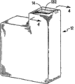
Fig. 1 is a kind of perspective view of printer 10, and above-mentioned printer 10 is used for printing on media 22 with print cartridge (or an ejection cartridge) 12.Fig. 2 is box 12 perspective views that one embodiment of the invention has printhead (or fluid drop generator or fluid ejection apparatus) 14.Fluid or ink spray or are released on the media 22 from nozzle 132.
Fig. 3 illustrates the enlarged drawing of 14 1 embodiment of printhead with perspective view.In this embodiment, printhead 14 has a plurality of parts, and comprising an edge ladder 119, above-mentioned edge ladder 119 is used for a kind of edge fluid and is fed into resistor (or fluid ejector) 61.Printhead also has a groove 124, and above-mentioned groove 124 partly is formed in the substrate surface.A groove (or passage) 126 is used for a kind of concentrated flow body and is fed into resistor 61, and/or a succession of feeding fluid also illustrates on this printhead to the hole 127 of resistor 61, and each groove or hole 127 all are to form with UV laser processing method as described herein.Groove 124 also can be with forming as following UV laser processing method furtherly.The parts that explanation at least two printheads 14 in Fig. 3 is arranged in one embodiment.For example, in printhead 14, only form feeding hole 127 and groove 126, in an alternative embodiment, also form edge ladder and/or groove 124 here.In another example, in printhead 14, form edge ladder 119 and groove 126, in an alternative embodiment, also form groove 124 and/or feeding hole 127 here.
Fig. 4 illustrates the cutaway view of the printhead 14 of Fig. 2, and the groove 126 that has groove (or side) wall 123 herein passes a substrate 102 and forms.Passing in the substrate groove zone (or groove area) forms groove and illustrates in greater detail below.In another embodiment, a kind of higher density groove of etching in the mould of a regulation.For example, spacing in mould or substrate between mutual separation and the adjacent slot is low to reach 10 microns (in one embodiment, 10 microns than each groove heat affected area scope one times high slightly, the heat affected area is to be subjected to the area that Laser Processing influences among the application along cell wall herein).
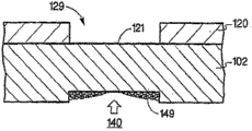
In Fig. 4, show a thin layer (or active layer, pellicular cascade, a conductive layer or have one deck of microelectronic component) 120, above-mentioned thin layer 120 is formed on or is arranged on the front or first side (or surface) 121 of substrate 102.First side 121 of substrate 102 is relative with (or surface) 122, second side of substrate 102.Pellicular cascade 120 is at the one deck at least that forms in the substrate with in a special embodiment, wherein at least a portion of 102 first sides 121 at the bottom of the masked radical.Alternatively or in addition, layer 120 makes wherein at least a portion electric insulation of substrate 102 first sides 121.
Shown in the printhead embodiment as shown in Figure 4, pellicular cascade 120 comprises a capping layer 104, a resistive layer 107, a conductive layer 108, a passivation layer 110, a cavitation barrier layer 111 and a barrier layer 112, above-mentioned each layer all form or are arranged on one or more layers the top of first side 121 of substrate 102 and/or front.In one embodiment, substrate 102 is a silicon.In various different embodiment, substrate is one of them of following material: monocrystalline silicon, polysilicon, GaAs, glass, quartz, pottery and a kind of semi-conducting material.The various materials of enumerating as possible base material not necessarily can exchange, and selected according to their application.In this embodiment, each thin layer forms figure and corrosion when suitable, so that form each resistance 61 in the resistive layer, the conductive trace in the conductive layer and a baking vessel 130 that is limited by the barrier layer at least in part.In a special embodiment, barrier layer 112 limits baking vessel 130, and fluid is by corresponding resistor heats herein, and limits a jet hole 132, and the fluid of heat is discharged by the said nozzle mouth.In another embodiment, a jet hole layer (not shown) with plurality of nozzles mouth 132 is added in 112 tops, barrier layer.An example of the actual arrangement in barrier layer, and the film fabric in February, 1994 number " Hewlett-PackardJournal " the 44th page of place illustrate.Other examples of ink jet-print head are in common U.S. Patent No. 4,719,477 of authorizing, U.S. Patent No. 5,317,346 and U.S. Patent No. 6,162,589 in statement.In an alternative embodiment, one deck or thin layer form or are deposited in the substrate 102 at least.Some embodiments of the present invention are included in and form in the substrate or any amount of deposit or the layer (perhaps not having layer) of type, and this depends on the application that utilizes the open flume type substrate.
In the embodiment shown in fig. 4, passage 129 forms hole or the fluid feeding groove 129 that is passed in each layer (120) of forming in the substrate.Passage 129 fluid-types connect baking vessel 130 and groove 126, so that fluid flows through groove 126 and flows into baking vessel 130 by passage 129.Shown in specific embodiment in, the feeder connection 129 that fluid is used is not or not the center of groove 126.Yet, being positioned at the center or departing from the center no matter under which kind of situation at inlet 129, open flume type substrate formation as described below is substantially the same.
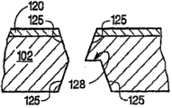
In the embodiment shown in Fig. 4 A and the 4B, the plane and the perspective view of printhead 14 and groove 126 thereof is shown, do not have barrier layer 112 (being used for Fig. 4 A) simultaneously and do not have lamination 120 (being used for Fig. 4 B).Shown in embodiment among Fig. 4 A, each resistor 61 all is along groove 126.Shown in embodiment among Fig. 4 B, cell wall 123 has some stripeds (or vertical line) 142, and near the fluting method of the present invention of a rough region (or penetrating region) 144 usefulness groove 126 middle parts forms.Rough region 144 is by penetrating formation near groove 126 central authorities.Therefore compare with the rooved face position,, during processing, less stress is arranged penetrating on the rough region 144 in this medial launder position moment of flexure minimum.As a result, penetrating rough region 144 places, and therefore in whole substrate 102 crackle minimum.Therefore, have 3 microns at the most by formed each groove of one embodiment of the invention along the chip size of substrate surface, if any.
Also as shown in Figure 4A and 4B, groove 126 has a mural margin 146.In one embodiment, mural margin 146 is about 3 microns and be about 5 microns along the roughness (or smoothness) of substrate second side 122 along the roughness (or smoothness) of substrate first side 121, although roughness can be more or less in this embodiment.
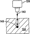
In the described embodiment of Fig. 5 A flow chart, at step 200 place, thin layer or lamination 120 form in wafer or substrate 102, shelter and constitute figure, so that form groove 129, as shown in Figure 6A.In an embodiment (not shown), on the substrate dorsal part 122 opposite, form a hard mask and/or the imageable material layer of a kind of light in addition with thin layer 120.At step 210 place, utilize a UV laser beam 140 (seeing Fig. 6 A) to aim at the formation of a substrate zone beginning groove to be slotted.In this embodiment, a zone on substrate second side 122 is the beginning zone of waiting to be exposed under the UV laser beam.Ablated and/or the evaporation of base material in the basal region under being exposed to the UV laser beam so that form groove 126, is described in more detail as following.
As shown in Figure 6A and 6B, formed along cell wall 123 and along the bottom of raceway groove by chip that Laser Processing produced or residue 149 beginnings, above-mentioned trench bottom forms in substrate.In some alternative embodiment, chip can be formed by polycrystalline and/or amorphous silica.Shown in the embodiment of Fig. 6 B, in step 210 end, substrate 102 is lasered a degree of depth X.
At step 220 place, laser beam 140 is by first side or the surface 121 of the groove alignment substrate in the pellicular cascade 120, as shown in Fig. 6 B.Groove is finished to degree of depth Y by substrate UV Laser Processing, and degree of depth X is greater than degree of depth Y herein, herein the X+Y=base depth.In first embodiment, Y is about 20 microns.In one second embodiment, X is about a times of Y.In one the 3rd embodiment, X is approximately identical with Y.In also having another embodiment, Y is greater than X.
At step 230 place of Fig. 5 A, to each groove 126 repeating step 210 and 220 in the mould (or substrate).About shown in Fig. 6 A and the 6B and among the embodiment of explanation because chip the material of deposit (or have) 149 in more shallow raceway groove than in darker raceway groove easier discharge through the passages of processing, so output raising under above-mentioned two-way processing situation.In addition, in X some embodiment greater than Y, most of chip of discharging the passage of process processing is discharged from dorsal part 122, thereby has limited the contamination amount of one or more effective layers 120 on substrate front side 121.In another approach, the UV laser-induced thermal etching is at first implemented and is implemented from second side 122 then from first side 121, so that join at penetrating region 144 places.
In this embodiment, Laser Processing is provided by a UV laser beam 140 (Fig. 6 A), and In a particular embodiment, is provided by a kind of diode pumping fortune formula solid state pulse UV laser instrument (diode-pumped solid-state pulsed UV laser).In another particular embodiment, UV laser instrument 140 derives from the Xise 200 Laser Machining Tool of the Xsil of Dublin manufacturing of Ireland.Lasing light emitter (shown in Fig. 9 A and 9B) 139 utilizes power in about 2-100 watt scope, and more preferably is about 4.5 watts.Laser beam has a wavelength and is (1060nm)/n or (1053nm)/n, n=2 herein, 3 or 4.In a specific embodiments, the UV wavelength is less than about 400nm, especially about 355nm.The pulse width of laser beam is about 15ns in this embodiment, and repetition rate is about 30kHz.It is about 5-100 micron that laser beam has diameter, and more particularly is about 30 microns in this embodiment.Among the unshowned herein embodiment, laser processing tool of the present invention has a debris extraction system, so that remove the chip 149 that is produced by Laser Processing.
In one embodiment of the invention, strong UV light is absorbed into less than about 1 micron treating in the ablator surface.Because luminous energy so concentrates on the near surface of material, so material heats rapidly, melts and evaporates.The mixture of steam and fusing drop is discharged fast then.Therefore, peripheral region (or heat affected zone) do not melt basically because of the so quick process that takes place or do not damage in addition basically, and do not have time enough to be used for a large amount of heat propagations to the peripheral region.The more deep explanation of process is shown " interaction of laser beam and material: physical principle and application " book at Martin von Allmen and Andress Blater, second revision, nineteen ninety-five, existing explanation in the 131-134 page or leaf.
In laser processing method of the present invention, because Laser Processing so is limited to the part, so can obtain more smooth and more accurate groove profile.Therefore, also have surface roughness by the formed groove of some embodiments of the invention and be 5 microns at the most.Yet, when the laser machine penetrates substrate and forms groove 126, near breakthrough point, have rough region or coarse point 144, as shown in the groove profile embodiment of Fig. 6 C and 6D.In these embodiments, near the rough region 144 the groove center is the deposition materials again that fragment produced by heating, and above-mentioned segment does not extract effectively owing to the degree of depth of raceway groove.These segments melt subsequently and solidify, and form chip 149.
Shown in Fig. 5 B, step 300 is identical with the step 200 of Fig. 5 A.It is identical with the step 210 of Fig. 5 A and 220 that step 310 and 320 can be thought, yet some difference is as follows.At first in step 310, each the slot part ground on the mould forms from second side 122.When laser beam is aimed at first side 121 in step 320, the groove that each part forms is finished then.In other words, in this embodiment, the step that does not repeat the front takes place.In one embodiment, utilize a beam splitter in step 310 from the second side part landform grooving and/or be used for step 320, finishing fluting from first side, wherein be described in more detail according to Fig. 8 A and 8B below the beam splitter.In an alternative embodiment, first side 121 stood laser processing procedure before second side 122, thereby step 310 and 320 is put upside down.
Shown in Fig. 5 C, step 400 is identical with the step 200 of Fig. 5 A.In step 410, the two or more grooves on mould or wafer partly form simultaneously from second side 122 of mould.In step 420, those two or more grooves 126 are 121 all formation simultaneously from the front side.Repeating step 410 and 420 in step 430 is until forming each groove.In one embodiment, two or more grooves pass through to form in step 420 with beam splitter described below simultaneously, or partly form in step 410.In an alternative embodiment, first side 121 stood laser processing procedure before second side 122, thereby step 410 and 420 is put upside down.
In another embodiment, can be with the thought combination of Fig. 5 B and 5C, so that partly form two or more grooves simultaneously from second side 122.Then, be completed into any groove (two or more grooves in groups simultaneously) from the mould front side by Laser Processing before, on mould, partly forming each groove (two or more grooves in groups simultaneously) from second side.In an alternative embodiment, first side 121 stood laser processing procedure before second side 122.
Shown in Fig. 5 D, step 500,510 and 520 and the step 200 of Fig. 5 A, 210 is identical with 220, and it is as follows to have some difference.In step 510, groove is to carry out Laser Processing and then in step 520, carry out Laser Processing from first side of substrate from second side.After Laser Processing was carried out in both sides, groove still also was not completed at groove because with step 220 after be completed on the contrary, Laser Processing does not penetrate substrate 102 fully.In step 530, the groove that part is formed carries out Laser Processing from second side once more, until penetrating.In step 540, to each the groove repeating step 510-530 on the mould.As alternative plan of step 540, to the groove implementation step 510 that each partly forms on second side, then to each partly forms on first side groove implementation step 520 with then to the groove implementation step 530 that each partly forms on second side, until penetrating.In another alternative embodiment, first side is partly carried out Laser Processing, then second side is partly carried out Laser Processing and take place to penetrate at last from first side then.
Shown in Fig. 5 E, step 600 is identical with step 200 and 210 with 610, and it is as follows to have some difference.After implementation step 610, carry out the first surface that Laser Processing is penetrated into substrate always from second side.In step 620, treat each groove 126 repeating step 610 that on mould, forms.In a unshowned alternative embodiment, in step 600, form barrier layer 112 with the pellicular cascade on substrate first side 121 120.In another alternative embodiment, step 600 is to implement after completing steps 620.In another alternative embodiment, the UV Laser Processing of groove is implemented from first side 121 of substrate fully.
Fig. 6 E-6L illustrates the various embodiment of a kind of groove profile in the substrate 102.Shown in each embodiment in, the groove profile is not shown to scale.Generally, the groove profile is narrower than illustrated.For the ease of observing for the purpose of the difference in each groove profile, each groove profile is being than generally wideer shown in these figure.Substrate 102 is shown in and has effective layer on first side of substrate the layer of microelectronic component (or have) 120 in these embodiments.Yet in some alternative embodiment, one or more effective layers 120 are on second side of substrate.Shown in wherein each embodiment of these embodiment in, the groove profile comprises that by one of them of above-mentioned laser processing method the two-way laser processing method forms.
Fig. 6 E illustrates a kind of embodiment with open flume type substrate 102 of staged cell wall 128.The cell wall 128 of Fig. 6 E has the sectional area of change, and 121 incremental reduce the sectional area of above-mentioned change from second surface 122 to first surface.In an illustrated embodiment, the sectional area of 2 ladders and 3 changes is arranged, they and 3 well width a, b, relevant with c.Well width a is contiguous first surface 121, and well width c is contiguous second surface 122, and well width b is between a and c.In an illustrated embodiment, well width a is 210 microns, and well width b is 220 microns, and well width c is 260 microns.In an alternative embodiment, at near the well width the first surface is in about 100 micrometer ranges of about 5-, and be in about 100-300 micrometer range near the well width the second surface, this is near the second surface well width greater than near the well width the first surface.Especially, near the well width the second surface is than near the well width the first surface greatly at least 10%.For example, near the well width second surface is about 140 microns, and near the well width first surface is about 50 microns.
In the embodiment shown in Fig. 6 E, the following formation of groove profile: form well width b and c from second side 122, form well width a from first side 121 then.In another embodiment, each well width forms consistently from second side 122.In one first embodiment, form well width a, form well width b then, form well width c then.In one second embodiment, form well width c, form well width b then, form well width a then.Yet, can imagine various additional embodiments, comprising forming well width b, form well width c then, form well width a then, especially all the more so when utilizing the two-way laser processing method.
The staged cell wall of embodiment shown in Fig. 6 E is by making laser beam trace line in a special pattern form on the particular side of substrate.For example, Fig. 7 E illustrates an embodiment, and laser beam is with a plurality of cookie cutter figure 156 trace line, so that form groove 126 herein.In this embodiment, the laser beam of institute's trace line is concentric elliptical shape: shape m basically, n, and p, and shape m is minimum ellipse herein, and shape p is maximum ellipse, as shown in Fig. 7 E.In about the described embodiment of Fig. 6 E, at first to shape n and p trace line, to shape m trace line, shape m is equivalent to well width a herein then, and shape n is equivalent to well width b, and shape p is equivalent to well width c.Under alternate embodiment situations more of the present invention, can imagine other trace line order.Laser beam gives the other embodiment of figure trace line shown in Fig. 7 A-7F and according to Fig. 7 A-7F explanation.
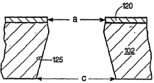
Fig. 6 F illustrates an embodiment of open flume type substrate 102, and it is taper and smooth cell wall 125 basically that above-mentioned open flume type substrate 102 has.The cell wall 125 of Fig. 6 F has the sectional area of change, and above-mentioned sectional area 121 incremental reduce from second surface 122 to first surface.In the embodiment shown, when groove profile during near first surface 121, the groove profile narrows down, and is expanded to first surface 121 a little then.Because the groove profile narrows down and expands near first surface in this embodiment, so with respect to first and second surfaces of substrate one asymmetrical timing hourglass shape is arranged.The groove density of contiguous first surface is denoted as a.The well width of contiguous second surface is denoted as C.The well width a of Fig. 6 F is identical with the well width of Fig. 6 E with c.
In one embodiment, cell wall 125 is by forming according to Fig. 6 A and the described method of 6B.When substrate is carried out Laser Processing and then when first side is carried out Laser Processing from second side, the penetrating region of groove has narrower as mentioned above sectional area and shown in Fig. 6 F.
In another embodiment, the cell wall 125 of Fig. 6 F forms by at first forming the groove profile shown in Fig. 6 E.In this embodiment, staged cell wall 128 is polished, so that form the tapered wall 125 of Fig. 6 F.The method that polishes is described in more detail below.In an alternative embodiment, the wall that polishes has a slight curvature.In another embodiment, the groove profile 121 diminishes from second surface 122 to first surface, does not have narrow sectional area simultaneously in the groove profile.
Fig. 6 G illustrates one, and to have one be the groove profile embodiment of sand glass formula shape basically, and this is in when penetrating in the silicon, forms the cross section 144 that narrows down near the middle part.Groove has tapered wall 125, and the two is tapered towards the middle part of groove from first and second surfaces of substrate 102 for above-mentioned tapered wall 125.This embodiment generally forms according to process chart 5A with above-mentioned bidirectional fluid groove.
Fig. 6 H illustrates one, and to have be the groove profile embodiment of straight trough wall basically.These cell walls form with the method that polishes described below.In one embodiment, these walls are by one of them formation of said method.
Fig. 6 I illustrates a groove profile embodiment with groove shape of a kind of mixing.Fig. 6 I illustrates a kind of groove profile with a sand glass formula shape, and above-mentioned groove profile has a countersunk in second surface.The embodiment of Fig. 6 I groove profile has wall surface 125 and wall surface 128, and above-mentioned wall surface 125 is tapered from each substrate surface, and 128 one-tenth stageds of above-mentioned wall surface, that is with the direction quadrature of laser beam, form countersunk simultaneously.In one embodiment, these walls 125 and 128 one of them formation at least by methods described herein.
Fig. 6 J illustrates a groove profile embodiment with groove shape of a kind of mixing.Fig. 6 J illustrates the groove profile that has a countersunk, and above-mentioned groove profile has a stepped walls 128.Fig. 6 J is to similar according to the described embodiment of Fig. 6 E, exception be that Fig. 6 J has only a ladder in the groove profile.The method of the Fig. 6 of being used to form E as herein described and other method that is used to form each cell wall when suitable, can be applied to this present embodiment shown in Fig. 6 J.
Fig. 6 K illustrates a groove profile embodiment with groove shape of a kind of mixing.Fig. 6 K illustrates a kind of groove profile with a sand glass formula shape, and above-mentioned groove profile has the countersunk of a biasing.The groove profile embodiment of Fig. 6 K has cell wall and cell wall with staged surface 128 and one conical surface 125 of a band conical surface 125, the cell wall of above-mentioned conical surface 125 describes shown in Fig. 6 G and according to Fig. 6 G, and above-mentioned cell wall with staged surface 128 and one conical surface 125 describes shown in Fig. 6 I and according to Fig. 6 I.In one embodiment, these walls are by one of them formation at least of methods described herein.
Fig. 6 L illustrates another embodiment of groove profile of the groove shape with a kind of mixing.Fig. 6 L illustrates a kind of groove profile that has the countersunk of setovering, and described groove profile has stepped walls 128.In an illustrated embodiment, the stepped walls on each side of groove is shifted so in the same direction, so that all keep substantially the same along the groove profile at the sectional area of all points basically.In one embodiment, these walls are by one of them formation at least of methods described herein.
Fig. 7 A-7F illustrates the laser beam figure, comprising the various embodiment in laser beam trace gap.Laser beam is aimed at a groove area on first surface 121 and the second surface 122 one of them (or the two) when forming open flume type substrate of the present invention.Added laser beam figure decision groove area, and therefore, the groove shape on the decision substrate surface.In a particular embodiment, when forming fluidic component, a laser beam figure repeatedly is added in the substrate.In another embodiment, when forming fluidic component, a plurality of laser beam figures are added in the substrate.In one first embodiment, each side of substrate/lip-deep groove area is about 260 microns * 8480 microns.In one second embodiment, the groove area on the first surface is that about 210 microns * 8480 microns and the groove area on second surface are about 260 microns * 8480 microns.In some alternative embodiment, well width is narrow to the 5-10 micron with widely reach 300 microns.At some more specifically among the embodiment, according to the application of fluid slot, well width is 30-50 micron or 80 microns.In most of embodiment, there is a low length-width ratio to increase Laser Processing speed, relevant because chip disturbs with the parts of high-aspect-ratio.In a specific embodiment, wish that herein each well width is narrow to the 5-10 micron, much bigger along the accumulation of debris ratio of cell wall greater than about 80 microns well width.
Fig. 7 A illustrates an embodiment, and laser beam trace line in a kind of grating or serpentine pattern 150 herein is so that form groove 126 in printhead 14.In an illustrated embodiment, the laser beam trace line begins at an end place of groove area, then in a longitudinal direction before and after trace line, vertically hold until the opposite that reaches groove.As shown in this embodiment, the gap between the adjacent laser beam trace is changeless basically.
Fig. 7 B illustrates an embodiment, herein laser beam a kind of be trace line in the spirality figure 152 basically so that form groove 126.The laser beam trace line begins in the center of groove, and moves in the circular pattern that a size increases gradually, so that form the shape of groove 126.In an alternative embodiment, the laser beam trace line begins along the edge of desirable groove shape, and size reduces gradually, and is to move in the figure of circle basically one simultaneously.
Fig. 7 C illustrates an embodiment, and laser beam is with a kind of cookie cutter figure 154 trace line, so that form groove 126 herein.In an illustrated embodiment, laser beam is along the edge trace line of groove 126 desirable groove shape.
Fig. 7 D illustrates an embodiment, and laser beam is with a kind of cookie cutter figure 154 trace line herein, as described in according to Fig. 7 C and shown in, and with raster graphic 150 trace line, as described in according to Fig. 7 A and shown in so that form groove 126.At first be figure 150 or 154 trace line.
Utilize a plurality of cookie laser beam figures 156 to be described above forming Fig. 7 E embodiment of a groove.In an alternative embodiment, in cookie formula laser beam figure, a plurality of traces are arranged, as two traces, perhaps many in fact as far as possible traces.For those embodiment as shown in Fig. 6 E, each laser beam trace becomes littler continuously (or bigger), and continuous laser beam is aimed at the degree of depth of lower (or higher) in the substrate.When number increased, it is more and more smooth that cell wall becomes when continuous laser beam trace (these traces are last slight change on the size and the degree of depth).
Fig. 7 F illustrates an embodiment, and laser beam is with a kind of window figure 158 trace line of modification, so that form groove 126 herein.In an illustrated embodiment, laser beam in the edge of groove 126 desirable groove shape with a kind of ring trace line of closure.In one first embodiment, all the closed loop than the front is big for each adjacent laser beam trace.In one second embodiment, all the closed loop than the front is little for each adjacent laser beam trace.Yet as shown in the figure, except near groove terminal, the gap maintenance between each adjacent traces immobilizes basically.In an illustrated embodiment, the closed loop of each adjacent laser beam trace all is superimposed upon on each groove end.In this embodiment, there are 4 closed loops to be superimposed upon each groove end.In some alternative embodiment, at least 2 closed loops are arranged.
Under situation of the present invention, can expect the various embodiment of some groove profiles, above-mentioned groove profile makes up each species stage, tapered wall, smooth wall and countersunk.
In some alternative embodiment or the embodiment except laser beam trace figure, the staged of embodiment shown in Fig. 6 A-6L, taper, cell wall smooth or that change in addition can form by changing Laser Processing, trace or laser beam source.The method of several change laser beams or Laser Processing is arranged, and said method can be used with various embodiments of the present invention.Some method in the said method comprises by moving laser beam foucing (towards substrate or away from substrate) change lasing beam diameter in the Z direction, reach the UV laser machine of regulating.For example, lasing beam diameter can change with a kind of optical beam expander.In a particular embodiment, optical beam expander (telescope) is Galiean (Jia Lilve looks in the distance), may not cause the internal focal point of air breakdown herein under high energy pulse formula laser condition.Alternatively, under lower energy, use the Keplerian telescope.To more optical beam expander information, see http://www.mellesgriot.com/pdf/002.10-2.12.pdf about reinstating with the present invention one.Sweep speed, pulse width, repetition rate, condenser lens, laser power etc. can be in UV laser machine adjusted, so that change laser beam or Laser Processing.For example, can laser power can be reduced in surface breakdown place or near so that make the damage of substrate surface, comprising peeling off and crackle (having the damage of groove edge in the surface of imitating layer in particular for minimizing) reduces to minimum.In another example, laser beam is defocused, so that purification tank and substrate.
Fig. 8 A-8B illustrates the various embodiment of optical plan that are used to divide laser beam 140.In the embodiment shown in these, laser beam 140 is from LASER Light Source 139.High energy pulse laser beam 140 splits into many penlights, so that each penlight all has optimum capacity, and therefore has the optimal etch degree of depth.In an illustrated embodiment, utilize the increase of laser power to produce two light beams with better condition.Fig. 8 A illustrates and utilizes conventional optical element split beam, and Fig. 8 B illustrates a kind of alternative embodiment that utilizes the diffraction optical element split beam.If adopt enough big optical element, then embodiments of the invention can be used for the light beam of virtually any size.In further embodiments, under situation of the present invention, can expect to have more than two the light beam or the penlight of optimum capacity.
Fig. 8 A illustrates the embodiment of one 50/50 beam splitter 180 of laser beam 140 directives, and laser beam splitting becomes two penlights herein.Wherein first penlight continues to advance in the same direction, and when arriving first condenser lens 184, focuses on the printhead 14 (or substrate), is used for the Laser Processing substrate.Second penlight reflects towards vertical direction, and penlight arrives soon after a minute surface 182 and reflection towards one second condenser lens 184, so that contiguous first penlight focuses on the printhead (or substrate).After this manner, two laser beams can be processed two grooves simultaneously in a substrate.
Fig. 8 B illustrates with diffraction optical element and makes beam splitting.Fig. 8 B illustrates the embodiment of a diffraction element 186 of laser beam 140 directives, and laser beam splitting becomes two penlights herein.Wherein each continues to advance to a condenser lens 184 towards substrate towards substantially the same direction two penlights.Each penlight focuses on substrate or the print head 14 the groove zone or treats on the zone of Laser Processing then.In this alternative mode, two laser beams can be processed suprabasil two grooves or two zones simultaneously.
Fig. 9 A-9B is illustrated in an embodiment of some steps of mobile laser beam foucing on the Z direction.In this embodiment, the lasing light emitter 139 of laser beam 140 from the primary importance shown in Fig. 9 A with respect to substrate 102 move to shown in Fig. 9 B with respect to one of substrate more approaching position.In an illustrated embodiment, pass that substrate adds and etch depth when increasing, lasing light emitter and the distance increase for the treatment of between the etched substrate when laser beam.As a result, in an illustrated embodiment, the focus of laser beam is not the amount increase that changes (because laser beam decay) and/or chip 149 best.As shown in the embodiment of Fig. 9 B, if under the deep etching situation mobile lasing light emitter, then the focus of laser beam keeps substantially the same throughput.In an alternative embodiment, under the situation that increases the degree of depth, regulate the focus of laser beam.
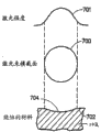
Figure 10 A-10B illustrates the laser beam power that is described on the lasing aperture or intensity and subsequently through the embodiment of overetched material profile.Figure 10 A is the embodiment that a laser beam 700 is described in a usefulness one laser intensity Gauss (Gaussian) distribution.In Figure 10 A, be illustrated in gauss laser power or intensity curve 701 on the laser beam cross-section.Laser beam 700 contact materials are the surface 702 in the zone that marks at dotted line basically.In this embodiment, laser beam 700 makes through overetched material band one curved surface 702.The central area 704 of material is bigger than the etched degree in edge or neighboring area, because bigger in the center intensity of laser beam.In certain embodiments, because uneven layout, so curved surface 702 may not be best.
Figure 10 B illustrates an embodiment of a kind of laser beam or " carnival hat " laser beam 800, and above-mentioned laser beam has uniform intensity to laser power.In Figure 10 B, show even laser power or intensity curve 801 on laser beam cross-section.In this embodiment, laser beam 800 is the surface in the dotted line 802 in Figure 10 B in the contact of surperficial 804 places basically.Although laser beam is not the zone of aiming at neighbouring surface 804 wittingly, also be commonly referred to as edge or neighboring area 806, these zones 806 are affected in certain embodiments.As shown in this embodiment, laser beam 800 makes that directly to have one in the zones of contact be flat surface 804 basically and have a curved surface along periphery 806 at laser beam 800 through overetched material.Because the uniform strength of laser beam is basically along entire cross section, so zone 804 basically by uniform etching, that is is flat.In certain embodiments, utilize (a) a kind of beam-expanding telescope, mask and imaging len, (b) diffraction optical element and/or (c) light beam homogenizing unit (as the segmentation minute surface) reach the light beam of uniform strength.
Therefore, be appreciated that the present invention can not resemble specify practical operation.For example, the invention is not restricted to hot activation formula printhead, but also can comprise for example piezoelectricity activation type printhead and other mechanical start type printhead, and other has the application of the microfluidic channels of the substrate of passing.The method of above-mentioned formation microfluidic channels also can be applied to Micro Electro Mechanical System (MEMS), and above-mentioned Micro Electro Mechanical System comprises that for example atom is differentiated storage device, fuel cell, sensor, and display.Therefore, some embodiments of the present invention see from which aspect and all should think and be exemplary and not restrictive that scope of the present invention is represented with appended claims, rather than used and state bright expression.Enumerate the place of its " " or " first " equivalence element in claim, this claim is understood to include installs one or more such elements, simultaneously both neither requiring nor excluding two or more this element.