CN1875456A - 用于双栅极晶体管半导体制造方法的限制性间隔件 - Google Patents
用于双栅极晶体管半导体制造方法的限制性间隔件 Download PDFInfo
- Publication number
- CN1875456A CN1875456A CNA2004800317887A CN200480031788A CN1875456A CN 1875456 A CN1875456 A CN 1875456A CN A2004800317887 A CNA2004800317887 A CN A2004800317887A CN 200480031788 A CN200480031788 A CN 200480031788A CN 1875456 A CN1875456 A CN 1875456A
- Authority
- CN
- China
- Prior art keywords
- fin
- gate electrode
- cap layer
- dielectric
- silicon
- Prior art date
- Legal status (The legal status is an assumption and is not a legal conclusion. Google has not performed a legal analysis and makes no representation as to the accuracy of the status listed.)
- Pending
Links
- 238000000034 method Methods 0.000 title claims abstract description 44
- 125000006850 spacer group Chemical group 0.000 title claims abstract description 35
- 230000008569 process Effects 0.000 title claims abstract description 21
- 239000004065 semiconductor Substances 0.000 title claims abstract description 12
- 238000004519 manufacturing process Methods 0.000 title abstract description 6
- XUIMIQQOPSSXEZ-UHFFFAOYSA-N Silicon Chemical compound [Si] XUIMIQQOPSSXEZ-UHFFFAOYSA-N 0.000 claims abstract description 59
- 229910052710 silicon Inorganic materials 0.000 claims abstract description 58
- 239000010703 silicon Substances 0.000 claims abstract description 58
- 238000005530 etching Methods 0.000 claims abstract description 27
- 239000000758 substrate Substances 0.000 claims abstract description 23
- 229920005591 polysilicon Polymers 0.000 claims abstract description 22
- 229910021420 polycrystalline silicon Inorganic materials 0.000 claims abstract description 21
- 229910021332 silicide Inorganic materials 0.000 claims abstract description 16
- FVBUAEGBCNSCDD-UHFFFAOYSA-N silicide(4-) Chemical compound [Si-4] FVBUAEGBCNSCDD-UHFFFAOYSA-N 0.000 claims abstract description 16
- 229920002120 photoresistant polymer Polymers 0.000 claims abstract description 12
- 239000000463 material Substances 0.000 claims description 51
- 230000015572 biosynthetic process Effects 0.000 claims description 13
- 239000000203 mixture Substances 0.000 claims description 12
- 229910052751 metal Inorganic materials 0.000 claims description 6
- 239000002184 metal Substances 0.000 claims description 6
- 150000004767 nitrides Chemical class 0.000 claims description 6
- 229910000577 Silicon-germanium Inorganic materials 0.000 claims description 5
- 239000000126 substance Substances 0.000 claims description 5
- 239000004020 conductor Substances 0.000 claims description 4
- 238000000151 deposition Methods 0.000 abstract 2
- 238000000059 patterning Methods 0.000 abstract 1
- 229910052581 Si3N4 Inorganic materials 0.000 description 7
- 238000012545 processing Methods 0.000 description 7
- HQVNEWCFYHHQES-UHFFFAOYSA-N silicon nitride Chemical compound N12[Si]34N5[Si]62N3[Si]51N64 HQVNEWCFYHHQES-UHFFFAOYSA-N 0.000 description 7
- NRTOMJZYCJJWKI-UHFFFAOYSA-N Titanium nitride Chemical compound [Ti]#N NRTOMJZYCJJWKI-UHFFFAOYSA-N 0.000 description 4
- 238000005516 engineering process Methods 0.000 description 4
- VYPSYNLAJGMNEJ-UHFFFAOYSA-N Silicium dioxide Chemical group O=[Si]=O VYPSYNLAJGMNEJ-UHFFFAOYSA-N 0.000 description 3
- 230000008901 benefit Effects 0.000 description 3
- 238000010438 heat treatment Methods 0.000 description 3
- 230000006872 improvement Effects 0.000 description 3
- RTAQQCXQSZGOHL-UHFFFAOYSA-N Titanium Chemical compound [Ti] RTAQQCXQSZGOHL-UHFFFAOYSA-N 0.000 description 2
- 238000006243 chemical reaction Methods 0.000 description 2
- 230000008021 deposition Effects 0.000 description 2
- 229910044991 metal oxide Inorganic materials 0.000 description 2
- 150000004706 metal oxides Chemical class 0.000 description 2
- 230000004048 modification Effects 0.000 description 2
- 238000012986 modification Methods 0.000 description 2
- 230000003647 oxidation Effects 0.000 description 2
- 238000007254 oxidation reaction Methods 0.000 description 2
- 238000001259 photo etching Methods 0.000 description 2
- 239000003870 refractory metal Substances 0.000 description 2
- MZLGASXMSKOWSE-UHFFFAOYSA-N tantalum nitride Chemical compound [Ta]#N MZLGASXMSKOWSE-UHFFFAOYSA-N 0.000 description 2
- 229910052719 titanium Inorganic materials 0.000 description 2
- 239000010936 titanium Substances 0.000 description 2
- ZAMOUSCENKQFHK-UHFFFAOYSA-N Chlorine atom Chemical compound [Cl] ZAMOUSCENKQFHK-UHFFFAOYSA-N 0.000 description 1
- 101100373011 Drosophila melanogaster wapl gene Proteins 0.000 description 1
- YCKRFDGAMUMZLT-UHFFFAOYSA-N Fluorine atom Chemical compound [F] YCKRFDGAMUMZLT-UHFFFAOYSA-N 0.000 description 1
- BPQQTUXANYXVAA-UHFFFAOYSA-N Orthosilicate Chemical compound [O-][Si]([O-])([O-])[O-] BPQQTUXANYXVAA-UHFFFAOYSA-N 0.000 description 1
- LEVVHYCKPQWKOP-UHFFFAOYSA-N [Si].[Ge] Chemical compound [Si].[Ge] LEVVHYCKPQWKOP-UHFFFAOYSA-N 0.000 description 1
- 229910045601 alloy Inorganic materials 0.000 description 1
- 239000000956 alloy Substances 0.000 description 1
- 239000013590 bulk material Substances 0.000 description 1
- 230000008859 change Effects 0.000 description 1
- 229910052801 chlorine Inorganic materials 0.000 description 1
- 239000000460 chlorine Substances 0.000 description 1
- 238000010276 construction Methods 0.000 description 1
- 238000013461 design Methods 0.000 description 1
- 238000011161 development Methods 0.000 description 1
- 230000000694 effects Effects 0.000 description 1
- 229910052731 fluorine Inorganic materials 0.000 description 1
- 239000011737 fluorine Substances 0.000 description 1
- 229910052735 hafnium Inorganic materials 0.000 description 1
- VBJZVLUMGGDVMO-UHFFFAOYSA-N hafnium atom Chemical compound [Hf] VBJZVLUMGGDVMO-UHFFFAOYSA-N 0.000 description 1
- 229910000449 hafnium oxide Inorganic materials 0.000 description 1
- WIHZLLGSGQNAGK-UHFFFAOYSA-N hafnium(4+);oxygen(2-) Chemical compound [O-2].[O-2].[Hf+4] WIHZLLGSGQNAGK-UHFFFAOYSA-N 0.000 description 1
- 239000012212 insulator Substances 0.000 description 1
- 238000001459 lithography Methods 0.000 description 1
- 229910052914 metal silicate Inorganic materials 0.000 description 1
- XZWYZXLIPXDOLR-UHFFFAOYSA-N metformin Chemical compound CN(C)C(=N)NC(N)=N XZWYZXLIPXDOLR-UHFFFAOYSA-N 0.000 description 1
- 229910021421 monocrystalline silicon Inorganic materials 0.000 description 1
- 210000004483 pasc Anatomy 0.000 description 1
- 230000004224 protection Effects 0.000 description 1
- 238000009418 renovation Methods 0.000 description 1
- 238000012958 reprocessing Methods 0.000 description 1
- 239000000377 silicon dioxide Substances 0.000 description 1
- 235000012239 silicon dioxide Nutrition 0.000 description 1
- 229910052715 tantalum Inorganic materials 0.000 description 1
- GUVRBAGPIYLISA-UHFFFAOYSA-N tantalum atom Chemical compound [Ta] GUVRBAGPIYLISA-UHFFFAOYSA-N 0.000 description 1
Images


Classifications
-
- H—ELECTRICITY
- H01—ELECTRIC ELEMENTS
- H01L—SEMICONDUCTOR DEVICES NOT COVERED BY CLASS H10
- H01L29/00—Semiconductor devices adapted for rectifying, amplifying, oscillating or switching, or capacitors or resistors with at least one potential-jump barrier or surface barrier, e.g. PN junction depletion layer or carrier concentration layer; Details of semiconductor bodies or of electrodes thereof ; Multistep manufacturing processes therefor
- H01L29/66—Types of semiconductor device ; Multistep manufacturing processes therefor
- H01L29/68—Types of semiconductor device ; Multistep manufacturing processes therefor controllable by only the electric current supplied, or only the electric potential applied, to an electrode which does not carry the current to be rectified, amplified or switched
- H01L29/76—Unipolar devices, e.g. field effect transistors
- H01L29/772—Field effect transistors
- H01L29/78—Field effect transistors with field effect produced by an insulated gate
- H01L29/785—Field effect transistors with field effect produced by an insulated gate having a channel with a horizontal current flow in a vertical sidewall of a semiconductor body, e.g. FinFET, MuGFET
-
- H—ELECTRICITY
- H01—ELECTRIC ELEMENTS
- H01L—SEMICONDUCTOR DEVICES NOT COVERED BY CLASS H10
- H01L21/00—Processes or apparatus adapted for the manufacture or treatment of semiconductor or solid state devices or of parts thereof
- H01L21/70—Manufacture or treatment of devices consisting of a plurality of solid state components formed in or on a common substrate or of parts thereof; Manufacture of integrated circuit devices or of parts thereof
- H01L21/77—Manufacture or treatment of devices consisting of a plurality of solid state components or integrated circuits formed in, or on, a common substrate
- H01L21/78—Manufacture or treatment of devices consisting of a plurality of solid state components or integrated circuits formed in, or on, a common substrate with subsequent division of the substrate into plural individual devices
- H01L21/82—Manufacture or treatment of devices consisting of a plurality of solid state components or integrated circuits formed in, or on, a common substrate with subsequent division of the substrate into plural individual devices to produce devices, e.g. integrated circuits, each consisting of a plurality of components
- H01L21/822—Manufacture or treatment of devices consisting of a plurality of solid state components or integrated circuits formed in, or on, a common substrate with subsequent division of the substrate into plural individual devices to produce devices, e.g. integrated circuits, each consisting of a plurality of components the substrate being a semiconductor, using silicon technology
- H01L21/8232—Field-effect technology
- H01L21/8234—MIS technology, i.e. integration processes of field effect transistors of the conductor-insulator-semiconductor type
- H01L21/823437—MIS technology, i.e. integration processes of field effect transistors of the conductor-insulator-semiconductor type with a particular manufacturing method of the gate conductors, e.g. particular materials, shapes
-
- H—ELECTRICITY
- H01—ELECTRIC ELEMENTS
- H01L—SEMICONDUCTOR DEVICES NOT COVERED BY CLASS H10
- H01L21/00—Processes or apparatus adapted for the manufacture or treatment of semiconductor or solid state devices or of parts thereof
- H01L21/70—Manufacture or treatment of devices consisting of a plurality of solid state components formed in or on a common substrate or of parts thereof; Manufacture of integrated circuit devices or of parts thereof
- H01L21/77—Manufacture or treatment of devices consisting of a plurality of solid state components or integrated circuits formed in, or on, a common substrate
- H01L21/78—Manufacture or treatment of devices consisting of a plurality of solid state components or integrated circuits formed in, or on, a common substrate with subsequent division of the substrate into plural individual devices
- H01L21/82—Manufacture or treatment of devices consisting of a plurality of solid state components or integrated circuits formed in, or on, a common substrate with subsequent division of the substrate into plural individual devices to produce devices, e.g. integrated circuits, each consisting of a plurality of components
- H01L21/822—Manufacture or treatment of devices consisting of a plurality of solid state components or integrated circuits formed in, or on, a common substrate with subsequent division of the substrate into plural individual devices to produce devices, e.g. integrated circuits, each consisting of a plurality of components the substrate being a semiconductor, using silicon technology
- H01L21/8232—Field-effect technology
- H01L21/8234—MIS technology, i.e. integration processes of field effect transistors of the conductor-insulator-semiconductor type
- H01L21/823468—MIS technology, i.e. integration processes of field effect transistors of the conductor-insulator-semiconductor type with a particular manufacturing method of the gate sidewall spacers, e.g. double spacers, particular spacer material or shape
-
- H—ELECTRICITY
- H01—ELECTRIC ELEMENTS
- H01L—SEMICONDUCTOR DEVICES NOT COVERED BY CLASS H10
- H01L29/00—Semiconductor devices adapted for rectifying, amplifying, oscillating or switching, or capacitors or resistors with at least one potential-jump barrier or surface barrier, e.g. PN junction depletion layer or carrier concentration layer; Details of semiconductor bodies or of electrodes thereof ; Multistep manufacturing processes therefor
- H01L29/66—Types of semiconductor device ; Multistep manufacturing processes therefor
- H01L29/66007—Multistep manufacturing processes
- H01L29/66075—Multistep manufacturing processes of devices having semiconductor bodies comprising group 14 or group 13/15 materials
- H01L29/66227—Multistep manufacturing processes of devices having semiconductor bodies comprising group 14 or group 13/15 materials the devices being controllable only by the electric current supplied or the electric potential applied, to an electrode which does not carry the current to be rectified, amplified or switched, e.g. three-terminal devices
- H01L29/66409—Unipolar field-effect transistors
- H01L29/66477—Unipolar field-effect transistors with an insulated gate, i.e. MISFET
- H01L29/66568—Lateral single gate silicon transistors
- H01L29/66613—Lateral single gate silicon transistors with a gate recessing step, e.g. using local oxidation
- H01L29/66628—Lateral single gate silicon transistors with a gate recessing step, e.g. using local oxidation recessing the gate by forming single crystalline semiconductor material at the source or drain location
-
- H—ELECTRICITY
- H01—ELECTRIC ELEMENTS
- H01L—SEMICONDUCTOR DEVICES NOT COVERED BY CLASS H10
- H01L29/00—Semiconductor devices adapted for rectifying, amplifying, oscillating or switching, or capacitors or resistors with at least one potential-jump barrier or surface barrier, e.g. PN junction depletion layer or carrier concentration layer; Details of semiconductor bodies or of electrodes thereof ; Multistep manufacturing processes therefor
- H01L29/66—Types of semiconductor device ; Multistep manufacturing processes therefor
- H01L29/66007—Multistep manufacturing processes
- H01L29/66075—Multistep manufacturing processes of devices having semiconductor bodies comprising group 14 or group 13/15 materials
- H01L29/66227—Multistep manufacturing processes of devices having semiconductor bodies comprising group 14 or group 13/15 materials the devices being controllable only by the electric current supplied or the electric potential applied, to an electrode which does not carry the current to be rectified, amplified or switched, e.g. three-terminal devices
- H01L29/66409—Unipolar field-effect transistors
- H01L29/66477—Unipolar field-effect transistors with an insulated gate, i.e. MISFET
- H01L29/66787—Unipolar field-effect transistors with an insulated gate, i.e. MISFET with a gate at the side of the channel
- H01L29/66795—Unipolar field-effect transistors with an insulated gate, i.e. MISFET with a gate at the side of the channel with a horizontal current flow in a vertical sidewall of a semiconductor body, e.g. FinFET, MuGFET
- H01L29/66818—Unipolar field-effect transistors with an insulated gate, i.e. MISFET with a gate at the side of the channel with a horizontal current flow in a vertical sidewall of a semiconductor body, e.g. FinFET, MuGFET the channel being thinned after patterning, e.g. sacrificial oxidation on fin
Abstract
一种半导体制造方法包括形成覆盖衬底的硅翼片。栅电介质被形成在翼片的主表面上。栅电极形成在翼片的至少两个表面上。然后在栅电极的侧壁附近有选择性地形成电介质间隔件并将其限制到此处,由此离开暴露的主翼片表面的大部分。此后,硅化物形成在主翼片表面上。在一种实施例中的栅电极的形成包括将多晶硅淀积在翼片和衬底上,将顶盖层淀积在多晶硅上,对在顶盖层上的光致抗蚀剂进行构图,以及通过顶盖层进行蚀刻。
Description
技术领域
本发明一般地涉及半导体制造领域,更具体地说,涉及利用双栅极或“翼片(fin)”FET晶体管的半导体制造方法。
背景技术
常规的金属氧化物半导体(MOS)具有这样的结构:其中在晶体管沟道区之上栅电极被中间栅电介质膜取代。在该沟道之下的区域包括体型衬底或者外延膜。通过将偏压施加给栅电极运行晶体管。体型材料同样地接地或被偏压到恒定电压。因此,常规的晶体管可以被描述为具有单侧栅极,因为栅极仅存在于该沟道的一侧(即之上)。
一般认为,单侧栅极晶体管固有地具有在操作上的特性,包括泄漏电流、驱动电流和亚阈值斜率,它们都小于理想值。这些参数在低功率应用中(比如无线技术中)特别严格。已经提出了多栅极晶体管结构来解决这个问题,在这种多栅极结构中栅电介质和栅电极形成在晶体管沟道的两侧(或更多侧)上。
多栅极晶体管的一个实例是“翼片”FET,如此命名是因为晶体管沟道是设置在下面的衬底之上的硅的翼片或壁。栅电介质形成在翼片的表面上,并且栅电极通过淀积并构图多晶硅或另一适合的材料而形成。翼片的暴露的部分(即没有被栅电极覆盖的部分)在所完成的晶体管结构中用作源极/漏极区。
减小在源极/漏极区中的电阻率对于包括多栅极晶体管的高性能晶体管的设计比较重要。这个目标通常至少部分地通过使用硅化物处理实现,在这种硅化物处理中与硅反应的材料比如钛淀积在晶体管上并在炉中被加热。在这个加热步骤中,只要淀积的材料接触暴露的硅就形成硅化物。暴露的硅包括暴露的源极/漏极区和基于硅的栅电极的上表面。通过在所暴露的硅面上有选择性地生长硅或硅锗至少可以部分地使得源极/漏极区的电阻率进一步降低。为防止在硅化物处理过程中在栅极和源极/漏极区之间形成电短路,在硅化物淀积之前在栅极侧壁附近形成电介质间隔件。硅化物材料不与下面的电介质反应。然后在硅化物加热处理之后清除没有反应的硅化物材料。
在基于翼片的处理中,如上文描述的常规的处理具有不理想的结果。具体地,在栅极蚀刻之后形成的电介质间隔件不仅形成在栅电极侧壁上,而且还形成在源极/漏极区中垂直取向的主翼片表面上(即没有被栅电极覆盖的翼片的区域)。因此,在间隔件形成之后,暴露出来的并能够被硅化的源极/漏极区部分仅仅是沿着非常小的翼片顶部表面。理想的是利用有选择性外延处理或者硅化处理或者两者的处理,在这种处理中暴露主翼片表面以用于硅化和/或选择性外延处理,同时仍然防止栅极到源极/漏极的短路。
发明内容
上文所述的问题通过包括形成覆盖衬底的硅翼片的半导体制造方法解决。栅电介质形成在翼片的主表面上。栅电极形成在翼片的至少两个表面上。在各种不同的实施例中,栅极材料可以包括一种或多种如下的材料的组合:包括多晶硅、多晶硅锗、氮化钛和氮化钽硅。然后在栅电极的侧壁附近有选择性地形成电介质间隔件并且将其限制在此,由此留下大部分主翼片表面被露出。此后,硅化物形成在主翼片表面上。在一个实施例中栅电极的形成包括将导电栅极材料淀积在翼片和衬底上,将顶盖层淀积在导电栅极材料上,对顶盖层之上的光致抗蚀剂构图,以及通过处于如下位置的经构图的光致抗蚀剂蚀刻穿过顶盖层和导电栅极材料:其中蚀刻产生了小于顶盖层的宽度的导电栅极材料宽度,以便在(其中可以形成限制性间隔件的)导电栅极材料的侧壁附近的顶盖层下形成空隙。
附图说明
通过参考下文结合附图的描述将会更好地理解本发明及其进一步的优点。
附图1-12所示为形成被限制到栅电极侧壁的间隔件的方法的第一实施例,其具有表示在处理步骤顺序中所选择的步骤的一系列部分截面剖视图;
附图13-19所示为形成被限制到栅电极侧壁的间隔件的方法的第二实施例,其具有表示在处理步骤顺序中所选择的步骤的一系列部分截面剖视图;和
附图20-28所示为形成被限制到栅电极侧壁的间隔件的方法的第三实施例,其具有表示在处理步骤顺序中所选择的步骤的一系列部分截面剖视图。
具体实施方式
现在详细地参考本发明目前优选的实施例,它们的实例在附图中示出。应该注意的是,附图是简化的形式,并没有按照精确的比例。虽然本发明在此参考某些所示出的实施例,但是应该理解的是这些实施例仅仅是举例,并不构成对本发明的限制。下文详细描述的目的是覆盖落在通过附加的权利要求所限定的本发明的精神和范围内的所有的改进、变更以及等同物。
将会理解的是,在此所描述的方法步骤和结构没有覆盖集成电路制造的完整处理流程。本发明通过结合本领域中常规地使用的各种集成电路制造技术实施,在此仅仅包括了为理解本发明所需要的普通地实施的处理步骤。
一般地说,本发明涉及使用硅翼片的多栅极晶体管的形成。在执行随后的外延或硅化物处理过程之前,未被栅电极覆盖的主翼片表面部分一直暴露到硅。暴露在翼片中的硅提高了随后处理的效率,并且形成了具有提高的电阻率和/或接触电阻的源极/漏极区。
现在转到附图,附图1至12所示为根据本发明的一种实施例的半导体制造处理顺序。在所描述的实施例中,翼片被首先形成在下面的衬底上。翼片用作最终晶体管的沟道区和源极/漏极区。在所描述的处理流程中,翼片通过如下方式形成:在包括硅衬底部分104和电介质部分102的衬底101上淀积电介质层106比如氮化硅层。在其它的实施例中,顶部电介质层106是可选择的。在一种实施例中,绝缘体上硅(SOI)晶片在下面的硅块材部分(没有绘制)上提供浅的单晶硅部分104和氧化硅部分102。在另一实施例中,所描述的衬底101可以通过在已存在的硅衬底上淀积氧化物(或其它的电介质)层102和硅层104而形成。
如附图2和附图3的截面图所示,然后通过如下的过程形成硅翼片114:对在附图1的电介质层106上覆盖的光致抗蚀剂层进行构图,曝光并显影光致抗蚀剂层,以及蚀刻通过层104和106的曝光部分以留下翼片114和顶盖电介质部分116。如附图2所示,在下面的衬底上的翼片114的垂直移位大致等于W/2,其中W表示在公知的比率W/L中的最终晶体管的电学宽度,比率W/L是晶体管的源极/漏极电流的主要决定因素。1/2的因子考虑了晶体管的两侧特性。因为多栅极晶体管(至少)具有两个活性表面,因此翼片的每个面对晶体管的宽度都有影响。
参考附图4和5的横截面视图,栅电介质层120形成在翼片114的主表面上,第一层122形成在翼片114和衬底层102上,顶盖层124淀积在第一层上。第一层122最终用作多栅极晶体管的栅电极。在优选的实施例中,第一层122是多晶硅层,而顶盖层124的材料被选择成相对于该材料可以有选择性地蚀刻第一层124。在第一层122例如是多晶硅的实施例中,顶盖层124可以是电介质,比如氧化物(例如SiO2)或氮化物(例如氮化硅)。在希望减小栅电极的电阻率的另一实施例中,顶盖层124是导电材料比如氮化钛等。在利用两种导电材料的另一实施例中,第一层122是导电层比如硅锗,同时顶盖层124是多晶硅。
在一种实施例中栅电介质层120的形成通过下面的翼片114的热氧化作用而实现。在其它的实施例中,栅电介质层120包括淀积的非导电的高-K的金属氧化物(例如氧化铪)或金属硅酸盐(例如硅酸铪)。
现在参考附图6的视图(截面)和附图7(平面),通过使用常规的光刻技术,通过首先形成覆盖附图4和5的顶盖层124的经构图的光致抗蚀剂层(没有绘制出)形成栅电极131。在光刻步骤之后,蚀刻顶盖层124和第一层122以产生如图所示的栅结构131。根据本发明的一种实施例的蚀刻顺序包括其中对顶盖层124进行构图以形成顶盖层部分134的第一蚀刻部分和其中进一步蚀刻下面的第一层122的第二蚀刻部分。
第一层122的蚀刻优选在如下的条件下使用对顶盖层部分134具有选择性的物质种类实施:在该条件下产生第一层122的相对各向同性的蚀刻以使第一层122相对于顶盖层部分134被底切。从这个蚀刻过程中得到的第一层部分142具有小于在它之上的顶盖层部分134之横向尺寸的横向尺寸(附图6)。在顶盖层134的突出部分之下直接产生的空隙实现限制性间隔件的形成,这种限制性间隔件防止了在硅化物形成过程中晶体管栅极与它的源极/漏极区短路。
在第一层122是多晶硅并且顶盖层124是耐火金属比如氮化钛的实施例中,蚀刻顺序可以包括第一部分和第二部分,在第一部分中在高真空和偏压下基于氯的蚀刻剂产生了顶盖层的高度各向异性蚀刻,之后在第二部分中在更小的偏压下基于氟的蚀刻剂产生了第一层122的有选择性的且底切的蚀刻。
现在分别转到附图8(截面)和9(平面),电介质间隔件144形成在顶盖层部分134的突出部分之下的空隙中。在一种实施例中,氮化硅淀积之后进行各向异性蚀刻。淀积填充位于第一层部分142的侧壁上的空隙,而蚀刻处理清除任何地方的氮化物,但除了受到上面的顶盖层134保护的氮化物之外。这样,电介质间隔件144被局限到第一层部分142的侧壁。如附图9所示,没有被栅结构131覆盖的硅翼片114的部分在间隔件144的形成之后被暴露。
暴露大部分硅翼片114,允许硅有选择性地生长在这个暴露的表面上,并且增强了通过随后的硅化物和外延处理实现的优点。参考附图10和12,执行有选择性的外延生长以形成附加的导电区或源极/漏极外延结构150,如附图11的截面剖视图所示(从上面)。厚的源极/漏极外延结构150减小源极/漏极电阻率,并且有利于随后到达源极漏极区的触点或通孔的形成。执行硅化物化处理顺序以使翼片114的暴露部分形成硅化物。在这个顺序中,适当的金属比如钽或钛被非选择性地淀积在晶片上并进行加热步骤。只要金属接触硅,在加热步骤中就形成了硅化物。受限制的间隔件144的存在防止了硅化物形成在第一层部分142的侧壁上,由此防止了在栅极电极和源极/漏极区之间的电路的形成(短路)。通过将栅极结构侧壁间隔件限制到靠近栅极结构的区域,外延结构150基本覆盖了硅翼片114的先前暴露的所有部分。
现在转到附图13至19,描述适合于在多栅极半导体工艺中制造被限制到接近晶体管栅结构侧壁的间隔件结构的方法的第二实施例。在这种实施方案中,翼片以与先前参考附图1至3所描述的相同方式形成。在如附图3所示的翼片形成之后,形成在附图14中的硅翼片114的主表面上所示的栅电介质120。
在形成硅翼片114和栅电介质120之后,执行多晶硅淀积,之后进行各向异性蚀刻(也称为间隔件蚀刻)以在硅翼片114主表面上任何地方产生多晶硅间隔件202(栅电介质120设置在它们之间的中间位置)。如附图15和16所示,顶盖材料210设置在多晶硅间隔件材料202上。与先前描述的顶盖材料一样,顶盖材料210是一种相对于在硅间隔件202中的硅能够被有选择性地蚀刻的材料,优选金属。在一种实施例中,顶盖层210是耐火金属比如氮化钛或者氮化钽硅。在另一实施例中,顶盖材料210是多晶硅,而间隔件202使用硅锗形成。
在形成硅间隔件202和顶盖层210之后,使用常规的光刻以形成栅极掩模光致抗蚀剂图形。此后,执行栅极蚀刻和整修过程以生产如附图17和18所示的栅极结构221。栅极结构221包括顶盖层210的剩余部分220和多晶硅间隔件202的剩余部分212。剩余的间隔件部分212相对于在附图17所示的顶盖层部分220被底切。这种底切产生了空隙211,该空隙211形成在凸伸的顶盖层之下的剩余间隔件部分212的侧壁附近。如附图19所示,通过淀积电介质比如氮化硅并执行各向异性蚀刻,在存在空隙211的地方形成电介质间隔件230。与附图10的电介质间隔件144类似,电介质间隔件230被限制到用作栅电极的剩余的(多晶硅)间隔件部分212的侧壁。暴露所述硅翼片114的剩余部分以用于随后的硅化物处理和有选择性的外延处理,如上文参考附图10至12所描述。
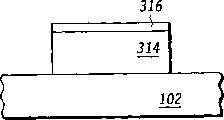
根据本发明的限制性间隔件处理顺序的第三实施例描述在附图20至28中。在本实施例中,翼片形成顺序产生比上面的顶盖电介质材料(例如氮化硅)316更薄的硅翼片314。使用相对各向同性干蚀刻整修所述硅翼片314以产生使顶盖电介质材料316从翼片314凸伸并在翼片314主表面之下和附近产生空间或空隙的底切效果。然后在硅膜314的主表面上形成栅电介质(例如通过热氧化)。附图22所示为从上面看的结构。
现在转到附图23至25,在多晶硅(或其它适合的栅电极材料)淀积之后进行掩模和蚀刻顺序以生产栅电极结构331,该栅电极结构包括导电栅电极330和电介质316的其余部分326。对栅电极330进行多晶硅蚀刻随后对层316进行蚀刻,形成了具有如附图23中所示的“肩状部”外形的电介质316的其余部分326。这可以通过留下锥形轮廓的对层316进行的干蚀刻或者在已经蚀刻了层316之后通过整修多晶硅来实现。从附图25的顶视图中可以看出,剩余的电介质326包括位于由栅电极330和硅翼片314限定的四个角落中的每个角落处的角部327。四个角部327覆盖用于形成限制性间隔件的下面的空隙。
如附图26至28所示,电介质间隔件340形成在电介质326的上方角部327之下。通过淀积电介质比如二氧化硅或氮化硅并各向异性地蚀刻已淀积的电介质层来形成间隔件340。间隔件340因此被限制在电介质326的角部327之下并在栅电极331的侧壁附近的区域。然后可以对硅翼片314的剩余部分进行有选择性外延和硅化物化。
在所描述的每个实施例中,通过形成限定位于栅电极侧壁附近的空隙的结构将间隔件限制到紧靠栅电极的附近,在该栅电极侧壁处空隙从上面被覆盖。然后通过淀积电介质并各向异性地蚀刻(除了被用于限定空隙的层从上面覆盖的地方之外的)全部地方来限制间隔件,不管该用于限定空隙的层是金属还是电介质比如氮化硅。一旦形成了限制性间隔件,则硅翼片的剩余的并被暴露的部分适合于硅化物化和选择性外延。在间隔件形成之后硅翼片的暴露面积的增加有利于实现低电阻且高性能的晶体管。
因此,对于受益于已经提供的本发明公开的教导的本领域普通技术人员来说,根据本发明制造实现上文阐述的集成电路的方法是很显然的。虽然参考本发明的特定的示例性实施例已经描述并示出了本发明,但是并不希望本发明限于那些示例性的实施例。本领域普通技术人员将会认识到在不脱离本发明的精神的前提下可以做出变型和改进。因此,希望在本发明内包括落在本发明的附加的权利要求及其等同物的范围内的所有这种变型和改进。
Claims (21)
1.一种半导体制造方法,包括:
形成覆盖衬底的硅翼片,该翼片具有基本垂直于所述衬底的表面的第一和第二主表面;
在所述硅翼片的第一和第二主表面上形成栅电介质;
形成覆盖所述栅电介质的栅电极;和
形成被限制在所述栅电极的侧壁附近的区域的电介质间隔件,其中主翼片表面在所述电介质间隔件的区域之外的部分被露出。
2.权利要求1的方法,其中进一步包括通过外延生长形成覆盖所述主翼片表面的暴露部分的附加导电区域。
3.权利要求2的方法,其中进一步包括:在覆盖所述主翼片表面的暴露部分的所述附加导电区域上形成硅化物。
4.权利要求1的方法,其中栅电极的形成限定了一部分栅电极的侧壁附近的限制性区域。
5.权利要求4的方法,其中形成栅电极的步骤包括:
在所述翼片和衬底上淀积第一材料;
在所述第一材料上淀积顶盖层,其中至少一种蚀刻剂在所述顶盖层和第一材料之间是有选择性的;
对覆盖所述顶盖层的光致抗蚀剂进行构图;
根据经构图的光致抗蚀剂蚀刻穿过所述顶盖层和第一材料,其中蚀刻步骤产生小于所述顶盖层的宽度的第一材料宽度,以进一步限定在第一材料侧壁附近在所述顶盖层之下的限制性区域。
6.权利要求5的方法,其中顶盖层是从由金属、多晶硅、氧化物和氮化物构成的材料组中选择的材料。
7.权利要求6的方法,其中从包括多晶硅和硅锗的材料组中选择第一材料。
8.权利要求5的方法,进一步包括非选择性地淀积电介质间隔件材料,并且随后蚀刻间隔件材料以便清除除了间隔件材料已经填充在多晶硅侧壁附近的限制性区域的地方之外的任何地方的电介质间隔件材料。
9.权利要求5的方法,进一步包括在淀积顶盖层之前执行第一材料的间隔件蚀刻。
10.权利要求1的方法,其中形成硅翼片的步骤包括:
淀积覆盖硅的顶盖电介质材料;
对覆盖所述顶盖电介质的光致抗蚀剂进行构图以暴露所述电介质材料的部分;和
对所述顶盖电介质的暴露部分和下面的硅进行蚀刻以形成翼片,其中蚀刻步骤包括相对于所述顶盖电介质对硅进行底切,其中硅翼片具有比顶盖电介质更薄的截面。
11.一种半导体制造方法,包括:
形成覆盖衬底的硅翼片,其中硅翼片包括基本垂直于下面的衬底的上表面的第一和第二主表面;
在所述硅翼片的主表面上形成栅电介质层;
形成与所述栅电介质层接触的栅电极,其中栅电极使得所述硅翼片的部分主表面被露出;
在所述栅电极的侧壁附近有选择性地形成电介质间隔件,其中电介质间隔件的部分主翼片表面在所述电介质间隔件形成之后仍然保持暴露状态;和
处理所述主翼片表面的暴露部分以减小它们的电阻率。
12.权利要求11的方法,其中处理主翼片表面的暴露部分的步骤包括:在主翼片表面的暴露部分上外延地生长硅。
13.权利要求11的方法,其中处理主翼片表面的暴露部分的步骤包括:在主翼片表面的暴露部分上形成硅化物。
14.权利要求13的方法,其中形成栅电极的步骤包括:
在所述翼片和衬底上淀积第一材料;
在第一材料上淀积顶盖层,其中至少一种蚀刻剂在所述顶盖层和第一材料之间是有选择性的;
对覆盖所述顶盖层的光致抗蚀剂进行构图;
根据经构图的光致抗蚀剂蚀刻穿过所述顶盖层和第一材料,其中蚀刻步骤产生小于顶盖层的宽度的第一材料宽度,以进一步限定在第一材料侧壁附近在顶盖层之下的限制性区域。
15.权利要求14的方法,其中顶盖层是从由金属、多晶硅、氧化物和氮化物构成的材料组中选择的材料。
16.权利要求15的方法,其中从包括多晶硅和硅锗的材料组中选择第一材料。
17.一种在集成电路内的晶体管,包括:
覆盖衬底的硅翼片,其中硅翼片包括基本垂直于下面的衬底的表面的第一和第二主表面;
在所述硅翼片的第一和第二主表面的至少一部分上的栅电介质;
覆盖所述栅电介质的栅电极,其中所述栅电极限定位于所述栅电极之下的所述硅翼片内的晶体管沟道区和在所述硅翼片的剩余部分之内的源极/漏极区;和
在所述栅电极的侧壁附近并且被限制在栅电极附近的电介质间隔件。
18.权利要求17的晶体管,其中栅电极包括第一材料和覆盖第一材料的顶盖层,其中第一材料的宽度小于顶盖层的宽度,其中电介质间隔件占据凸伸在第一材料之上的顶盖层部分之下的区域。
19.权利要求17的晶体管,其中第一材料是硅,顶盖层是从由金属、氧化物和氮化物构成的材料组中选择的材料。
20.权利要求17的晶体管,进一步包括形成在没有被栅电极覆盖的硅翼片部分上的附加导电材料,其中被限制的间隔件阻止了在所述附加导电材料和栅电极之间的导电。
21.一种半导体制造方法,包括:
形成覆盖衬底的硅翼片,该翼片具有基本垂直于衬底的表面的第一和第二主表面;
在所述硅翼片的第一和第二主表面上形成栅电介质;
形成覆盖所述栅电介质的栅电极;
形成覆盖所述栅电极的顶盖层并对所述顶盖层进行构图,其中顶盖层形成覆盖所述栅电极且横向尺寸大于下面栅电极之横向尺寸的顶盖,进一步形成位于栅电极的侧壁附近的限制性区域;和
形成被限制在栅电极侧壁附近的限制性区域内的电介质间隔件,其中主翼片表面在电介质间隔件的区域之外的部分被露出。
Applications Claiming Priority (2)
| Application Number | Priority Date | Filing Date | Title |
|---|---|---|---|
| US10/695,163 US6951783B2 (en) | 2003-10-28 | 2003-10-28 | Confined spacers for double gate transistor semiconductor fabrication process |
| US10/695,163 | 2003-10-28 |
Publications (1)
| Publication Number | Publication Date |
|---|---|
| CN1875456A true CN1875456A (zh) | 2006-12-06 |
Family
ID=34549969
Family Applications (1)
| Application Number | Title | Priority Date | Filing Date |
|---|---|---|---|
| CNA2004800317887A Pending CN1875456A (zh) | 2003-10-28 | 2004-10-20 | 用于双栅极晶体管半导体制造方法的限制性间隔件 |
Country Status (6)
| Country | Link |
|---|---|
| US (1) | US6951783B2 (zh) |
| EP (1) | EP1683186A4 (zh) |
| JP (1) | JP2007510308A (zh) |
| CN (1) | CN1875456A (zh) |
| TW (1) | TWI350000B (zh) |
| WO (1) | WO2005045892A2 (zh) |
Cited By (1)
| Publication number | Priority date | Publication date | Assignee | Title |
|---|---|---|---|---|
| CN102956692A (zh) * | 2011-08-19 | 2013-03-06 | 阿尔特拉公司 | 缓冲型finFET器件 |
Families Citing this family (19)
| Publication number | Priority date | Publication date | Assignee | Title |
|---|---|---|---|---|
| US7354831B2 (en) * | 2005-08-08 | 2008-04-08 | Freescale Semiconductor, Inc. | Multi-channel transistor structure and method of making thereof |
| US7341902B2 (en) * | 2006-04-21 | 2008-03-11 | International Business Machines Corporation | Finfet/trigate stress-memorization method |
| US7442590B2 (en) * | 2006-04-27 | 2008-10-28 | Freescale Semiconductor, Inc | Method for forming a semiconductor device having a fin and structure thereof |
| US20070257322A1 (en) * | 2006-05-08 | 2007-11-08 | Freescale Semiconductor, Inc. | Hybrid Transistor Structure and a Method for Making the Same |
| EP1863097A1 (en) * | 2006-05-29 | 2007-12-05 | Interuniversitair Microelektronica Centrum ( Imec) | Method for modulating the effective work function |
| EP1863072A1 (en) * | 2006-05-29 | 2007-12-05 | Interuniversitair Microelektronica Centrum ( Imec) | Method for modulating the effective work function |
| US20080029827A1 (en) * | 2006-08-04 | 2008-02-07 | Ibrahim Ban | Double gate transistor, method of manufacturing same, and system containing same |
| US7691690B2 (en) * | 2007-01-12 | 2010-04-06 | International Business Machines Corporation | Methods for forming dual fully silicided gates over fins of FinFet devices |
| US7772048B2 (en) * | 2007-02-23 | 2010-08-10 | Freescale Semiconductor, Inc. | Forming semiconductor fins using a sacrificial fin |
| US8258035B2 (en) * | 2007-05-04 | 2012-09-04 | Freescale Semiconductor, Inc. | Method to improve source/drain parasitics in vertical devices |
| US7476578B1 (en) | 2007-07-12 | 2009-01-13 | International Business Machines Corporation | Process for finFET spacer formation |
| US8174055B2 (en) * | 2010-02-17 | 2012-05-08 | Globalfoundries Inc. | Formation of FinFET gate spacer |
| US8835261B2 (en) | 2011-03-14 | 2014-09-16 | International Business Machines Corporation | Field effect transistor structure and method of forming same |
| US9548213B2 (en) | 2014-02-25 | 2017-01-17 | International Business Machines Corporation | Dielectric isolated fin with improved fin profile |
| US20150372107A1 (en) * | 2014-06-18 | 2015-12-24 | Stmicroelectronics, Inc. | Semiconductor devices having fins, and methods of forming semiconductor devices having fins |
| US10062779B2 (en) | 2015-05-22 | 2018-08-28 | Taiwan Semiconductor Manufacturing Co., Ltd. | Semiconductor device and manufacturing method thereof |
| US10833175B2 (en) * | 2015-06-04 | 2020-11-10 | International Business Machines Corporation | Formation of dislocation-free SiGe finFET using porous silicon |
| US9558950B1 (en) | 2015-08-19 | 2017-01-31 | International Business Machines Corporation | Overhang hardmask to prevent parasitic epitaxial nodules at gate end during source drain epitaxy |
| US9472649B1 (en) | 2015-12-09 | 2016-10-18 | The United States Of America As Represented By The Secretary Of The Air Force | Fabrication method for multi-zoned and short channel thin film transistors |
Family Cites Families (13)
| Publication number | Priority date | Publication date | Assignee | Title |
|---|---|---|---|---|
| US6252284B1 (en) * | 1999-12-09 | 2001-06-26 | International Business Machines Corporation | Planarized silicon fin device |
| DE10012112C2 (de) * | 2000-03-13 | 2002-01-10 | Infineon Technologies Ag | Steg-Feldeffekttransistor und Verfahren zum Herstellen eines Steg-Feldeffekttransistors |
| JP4044276B2 (ja) * | 2000-09-28 | 2008-02-06 | 株式会社東芝 | 半導体装置及びその製造方法 |
| US6413802B1 (en) * | 2000-10-23 | 2002-07-02 | The Regents Of The University Of California | Finfet transistor structures having a double gate channel extending vertically from a substrate and methods of manufacture |
| US6475869B1 (en) * | 2001-02-26 | 2002-11-05 | Advanced Micro Devices, Inc. | Method of forming a double gate transistor having an epitaxial silicon/germanium channel region |
| JP3543117B2 (ja) * | 2001-03-13 | 2004-07-14 | 独立行政法人産業技術総合研究所 | 二重ゲート電界効果トランジスタ |
| US6635923B2 (en) * | 2001-05-24 | 2003-10-21 | International Business Machines Corporation | Damascene double-gate MOSFET with vertical channel regions |
| US6492212B1 (en) * | 2001-10-05 | 2002-12-10 | International Business Machines Corporation | Variable threshold voltage double gated transistors and method of fabrication |
| KR100458288B1 (ko) * | 2002-01-30 | 2004-11-26 | 한국과학기술원 | 이중-게이트 FinFET 소자 및 그 제조방법 |
| US20030151077A1 (en) * | 2002-02-13 | 2003-08-14 | Leo Mathew | Method of forming a vertical double gate semiconductor device and structure thereof |
| US6657252B2 (en) * | 2002-03-19 | 2003-12-02 | International Business Machines Corporation | FinFET CMOS with NVRAM capability |
| US6635909B2 (en) * | 2002-03-19 | 2003-10-21 | International Business Machines Corporation | Strained fin FETs structure and method |
| JP4410685B2 (ja) * | 2002-12-19 | 2010-02-03 | インターナショナル・ビジネス・マシーンズ・コーポレーション | フィン型fetを形成する方法 |
-
2003
- 2003-10-28 US US10/695,163 patent/US6951783B2/en not_active Expired - Lifetime
-
2004
- 2004-10-20 CN CNA2004800317887A patent/CN1875456A/zh active Pending
- 2004-10-20 WO PCT/US2004/035349 patent/WO2005045892A2/en active Application Filing
- 2004-10-20 JP JP2006538154A patent/JP2007510308A/ja active Pending
- 2004-10-20 EP EP04796345A patent/EP1683186A4/en not_active Withdrawn
- 2004-10-28 TW TW093132651A patent/TWI350000B/zh not_active IP Right Cessation
Cited By (2)
| Publication number | Priority date | Publication date | Assignee | Title |
|---|---|---|---|---|
| CN102956692A (zh) * | 2011-08-19 | 2013-03-06 | 阿尔特拉公司 | 缓冲型finFET器件 |
| CN102956692B (zh) * | 2011-08-19 | 2016-12-21 | 阿尔特拉公司 | 缓冲型finFET器件 |
Also Published As
| Publication number | Publication date |
|---|---|
| EP1683186A2 (en) | 2006-07-26 |
| WO2005045892A9 (en) | 2006-06-22 |
| US6951783B2 (en) | 2005-10-04 |
| US20050101069A1 (en) | 2005-05-12 |
| EP1683186A4 (en) | 2010-09-22 |
| WO2005045892A2 (en) | 2005-05-19 |
| WO2005045892A3 (en) | 2005-09-15 |
| TWI350000B (en) | 2011-10-01 |
| JP2007510308A (ja) | 2007-04-19 |
| TW200524160A (en) | 2005-07-16 |
Similar Documents
| Publication | Publication Date | Title |
|---|---|---|
| CN1875456A (zh) | 用于双栅极晶体管半导体制造方法的限制性间隔件 | |
| JP5299928B2 (ja) | Uゲートトランジスタ製造方法 | |
| CN100413039C (zh) | 形成FinFET装置中的栅极以及薄化该FinFET装置的沟道区中的鳍的方法 | |
| CN2751447Y (zh) | 多重栅极晶体管 | |
| JP4745663B2 (ja) | ダブルゲートFin−FETデバイスを形成する方法 | |
| US7105894B2 (en) | Contacts to semiconductor fin devices | |
| JP4966153B2 (ja) | 電界効果トランジスタおよびその製造方法 | |
| JP2006505949A (ja) | 半導体デバイスのゲートのクリティカルディメンションを改善するためのゲート材料のプレーナ化 | |
| US7605039B2 (en) | Multiple-gate MOS transistor using Si substrate and method of manufacturing the same | |
| JPH08167718A (ja) | Mis型fetおよびその製造方法 | |
| US6509609B1 (en) | Grooved channel schottky MOSFET | |
| WO2011134274A1 (zh) | 一种不对称型源漏场效应晶体管的制备方法 | |
| US20050224880A1 (en) | Multi-gate MOS transistor and method of manufacturing the same | |
| JP2008028263A (ja) | 半導体装置 | |
| TW201933492A (zh) | 半導體裝置的形成方法 | |
| JP2005051140A (ja) | 半導体装置およびその製造方法 | |
| JP2008098640A (ja) | 半導体装置の製造方法 | |
| TWI748346B (zh) | 多閘極之半導體結構及其製造方法 | |
| JP3444931B2 (ja) | 半導体装置及びその製造方法 | |
| KR100419744B1 (ko) | 트랜지스터 및 그의 제조 방법 | |
| KR102133208B1 (ko) | 펀치스루 스토퍼가 배제된 전계효과 트랜지스터 및 이의 제조방법 | |
| CN114765217A (zh) | 半导体装置 | |
| CN2722434Y (zh) | 使用多栅极晶体管的互补金属氧化物半导体晶体管反向器 | |
| TW201727891A (zh) | 半導體裝置 | |
| CN117476463A (zh) | 半导体结构及其形成方法 |
Legal Events
| Date | Code | Title | Description |
|---|---|---|---|
| C06 | Publication | ||
| PB01 | Publication | ||
| C10 | Entry into substantive examination | ||
| SE01 | Entry into force of request for substantive examination | ||
| C02 | Deemed withdrawal of patent application after publication (patent law 2001) | ||
| WD01 | Invention patent application deemed withdrawn after publication |