EP0021404B1 - Computing system for the simulation of logic operations - Google Patents
Computing system for the simulation of logic operations Download PDFInfo
- Publication number
- EP0021404B1 EP0021404B1 EP80103561A EP80103561A EP0021404B1 EP 0021404 B1 EP0021404 B1 EP 0021404B1 EP 80103561 A EP80103561 A EP 80103561A EP 80103561 A EP80103561 A EP 80103561A EP 0021404 B1 EP0021404 B1 EP 0021404B1
- Authority
- EP
- European Patent Office
- Prior art keywords
- logic
- processor
- instruction
- memory
- data
- Prior art date
- Legal status (The legal status is an assumption and is not a legal conclusion. Google has not performed a legal analysis and makes no representation as to the accuracy of the status listed.)
- Expired
Links
Images


Classifications
-
- G—PHYSICS
- G06—COMPUTING; CALCULATING OR COUNTING
- G06F—ELECTRIC DIGITAL DATA PROCESSING
- G06F30/00—Computer-aided design [CAD]
- G06F30/30—Circuit design
- G06F30/32—Circuit design at the digital level
- G06F30/33—Design verification, e.g. functional simulation or model checking
Definitions
- the advantages offered by the invention are that due to the parallel arrangement of the simulating computing system, the cost of the simulation is decreased and the speed and capacity are increased.
- the logic simulation machine Since the logic simulation machine is not a general purpose computer, it must be used as a device attached to a computer, which can perform functions such as compilation, input/output control, etc.
- the system in which the logic simulation machine will initially be used actually contains two general purpose computers in addition to the logic simulation machine.
- inter-processor switch 33 in a logic simulation machine 50. It provides communication among the thirty-one basic processors and between them and the control processor 32. Its primary purpose is to communicate simulated logic signals from the basic processor generating them to basic processors using them. In addition, it provides communication between the basic processors 1-31 and the control processor 32 for loading the basic processors, transferring inputs and outputs to the local computer, etc.
- the logic functions specified in the logic simulation machine instructions are defined by the contents of another basic processor memory, the function memory 37 shown in Fig. 1.
- the relation of the function memory 37 to other basic processor elements is illustrated in Fig. 1.
- the first instruction in the table selects an immediate logical 0 as its sixth input.
- the other two use the previous instruction's output as the sixth input, so their immediate fields are irrelevant (indicated by Xs in the table).
- the functions shown (two ORs followed by a NOR) cause the last instruction's output to be the NOR of all 15 inputs.
- the output of the logic unit which is the value stored in next signal value memory, is a function (AND or OR) of the current dot accumulator contents and the output of the current instruction (logic unit accumulator contents). This final value may be saved in the dot accumulator by using the SAVE FOR DOT flag.
- the logic unit accumulator contents for the current instruction is stored directly into the next signal value memory. No interaction with the current contents of the dot accumulator occurs.
- each basic processor has two additional internal logic data memories. These are identical to the current and next signal value memories 35 and 36 previously discussed. Like the signal value memories 35 and 36, these additional memories alternately assume one of two roles: that of the current signal input memory 38 and that of the next signal input memory 39. Their functions will be described in terms of these roles.
- the actual data memories have been called the A-IN memory and the B-IN memory.
- the current and next signal input memories 38 and 39 contain representations of logic signals. Both have 1024 locations, each holding one signal.
- the data in current signal input memory 38 are logic signal values that are currently present in the simulation, and were generated by other basic processors. This data is selected by use of ADDRESS SOURCE flags in each basic processor instruction. Each of the five addresses in an instruction has an associated ADDRESS SOURCE flag. When it is 0, the address references data in current signal value memory; when 1, the address references data in current signal input memory. Thus any or all of the data used in computing logic function can come from other processors.
- next signal input memory 39 In the course of a major cycle, updated values are obtained from the inter-processor switch 33 and placed in the next signal input memory 39; and at the end of each major cycle, the former next signal input memory is designated to be the current signal input memory (and visa versa).
- the switch select memory 40 of each basic processor has 1024 locations, each containing the address of a basic processor.
- the inter-processor switch 33 uses the switch select memory 40 to place updated logic signal values in the next signal input memory 39 as follows:
- the table of Fig. 11 shows a 2 in processor 3's 49th switch select memory location. This places the needed value in processor 3's 49th next signal input memory 39, so the table of Fig. 12 shows processor 3's 18th instruction accessing that location with its second address.
- the other table elements are derived similarly. It should be noted that at minor cycle 18, Processor 1 simultaneously transmits and receives, sending data to Processors 2 and 3 and obtaining it from Processor 3.
- the scheduling problem must be solved by the logic simulation machine compiler for each device to be simulated. Just as physical components must be placed and wired, simulated logic must be partitioned among the processors and scheduled.
- the control processor 32 of the logic simulation machine provides two functions of particular interest, they are organizing signal values into functional groups so that they can read from or write into the logic simulation machine with a single local computer (51) input/output operation, and halting the logic simulation machine and interrupting the local computer when any of a group of selected signals are set to specified values.
- the first function provides for efficient application of input sequences and gathering of data by the local computer.
- the halting function is the basic mechanism for informing the local computer of events in the simulation such as user-defined events or requests for array read or write.
- the control processor including these two functions are discussed as follows.
- the control processor also provides general logic simulation machine control function, such as, starting the logic simulation machine, halting it, etc. These are provided via commands from the local computer which utilize the control processor in a transparent manner.
- the control processor contains six memories referred to as a switch select memory, an output signal memory, an input signal memory, an output permutation memory, an input permutation memory, and an event mask.
- the input and output signal memories serve as a sink and a source, respectively, of logic data communicated between the control processor 32 and the basic processors 1-31 via the inter- processor switch 33. Both has 1024 locations, each holding a single signal.
- the function of the input and output permutation memories is to permute the transmission order of values in the input and output signal memories respectively.
- Each of these memories contains 1024 locations of 10 bits each; an address in the associated signal memory is contained in each location.
- This permutation of signal order allows data to be functionally grouped in the output signal memory, minimizing the local computer input/output operations needed to alter it. Such functional grouping might otherwise be impossible to achieve, due to the requirements of scheduling inter- processor data transfers through the inter-processor switch 33.
- a set of test inputs can be positioned in contiguous locations of the output signal memory and stored there with a single local computer input/output operation; appropriate output permutation memory contents can then feed that data to the switch at the minor cycles to which they have been scheduled for conflict-free inter- processor communication.
- the event mask contains 1024 locations of 4 bits each. Each of the bits corresponds to an individual value of the 2-bit code for simulated signal values: the first bit corresponds to 00, the second to 01, the third to 10, and the last to 11.
- the event mask in parallel with the output and input permutation memories of control processor 32, is cycled through in address order as part of a major cycle. As each signal value is received from the inter-processor switch 33, it is matched against the contents of the current event mask location. If the location contains a "1" corresponding to the signal value, the simulator is halted at the end of the current major cycle and an interrupt is presented to the local computer.
- event mask locations correspond to signal values in the order they are received from the switch, not in the (permuted) order of storage in input signal memory.
- any of several values of a particular signal can be made to cause the simulator to halt.
- the simulator could be halted when a particular signal is set to anything except logical 0.
- the control processor also contains two identical counters called level counter 1 and level counter 2, each 16 bits long. They can be loaded via local computer input/output commands, and are decremented each major cycle. When either reaches 0, the local computer is interrupted.
- These counters can be used for various purposes. For example, one can count the major cycles (gate delays) per logic cycle of the simulated device, giving the local computer an interrupt when it is time to gather an output vector and apply a new input vector. The other can count the total number of major cycles a simulation is to run.
- control processor 32 also shown in Fig. 1, which is shown on Fig. 13C and 13D. Control processor 32 will be described in detail later and as previously stated is used mainly to accumulate the result and to provide the control pulses which are needed for the entire logic simulation machine of this embodiment.
- the B and B IN memories will be read.
- the switching between the A and A IN and the B and B IN memories is accomplished by the switching mechanism indicated by the dotted line 212 on Fig. 13A. If it be assumed that, in a certain major cycle, the A and A IN memories are read out of in this same major cycle, the B and B IN memories can be read into. When the A and A IN memories are read out of, these two memories are regarded as a single memory.
- the A and the A IN are both memories addressed by the low order ten bits of the operand in register 206 while the high order bit of this same operand selects which of the two (A or A IN) memories is actually read. In other words, the operands in register 206 are eleven bits.
- each one of these memories are regarded as separate memories and are both addressed by ten bits which is contained in the address register 214 on Fig. 13A. These memories will be described in much more detail later on in the description.
- the pulse produced by the AND circuit 270 at this time extends the flip flop device 256 to reset it to its "0" state thus turning off the pulse generator 258.
- the same pulse is also applied to gate 262 in order to test "event latch” 260. If the latch 260 is still on its “0” state, a pulse will be produced on wire 272, which extends through OR circuit 248 to again turn “on” single shot device 250 in order to start a new major cycle. If the "event latch” 260 is in its "1” state, a pulse will appear on lead 274 to signal the end of operations.
- This timing chart of Fig. 13E will be understood better when the detailed circuits shown in the remaining figures are described.
- Figs. 16A and 16B arranged as shown in Fig. 16 which is a detail of the inter-processor switch which is indicated in Fig. 1 and by the dotted lines on the left side of Figs. 13A and 13D.
- the inter-processor switch has its own address counter 290 which supplies addresses to the switch memory 292.
- Memory words are placed into the register 294 by the P-1 gate pulse and later transferred to register 296 by the P-2 gate pulse.
- the groups of leads from each one of these decoders is applied to gates such as 298, 300, 302 and 304.
- FIG. 17A shows how the information in the register 216, which is also shown on Fig. 13B, refers to the logic unit for step one and how the control bits are directed to gates which suitably control the logic.
- the results of the logic unit first step are passed along with certain of the control bits in register 216 (Fig. 13B) to the logic unit second step shown in Fig. 17B.
- the Boolean logic equations for the logic unit second step are shown in Fig. 17B and it is believed that there will be no difficulty in understanding the operation of this unit.
- the "logic unit first step” shown in Fig. 17A carries out specific logic functions.
- the inputs to “logic unit first step” accepts and as shown in Fig. 17A.
- conventional logic circuits such as AND gates, OR gates and inverters arranged in a manner well known to those skilled in the art, the following logic operations are performed by the logic unit first step.
- FIG. 18 shows the details of event logic of Fig. 13C.
- the event logic is shown on Fig. 13C with one of its inputs coming from the mask field in register 240 and its input from the cable 244 which comes from the inter-processor switch.
- the data from the mask field in register 240 combines with the data from the inter-processor switch to produce an output of the OR circuit 322 which provides an output on line 324 in order to set the "event latch" 260 to its "1" state. Then, it is said that an "event” has occurred.
- the detection of an "event” causes a signal to appear on lead wire 274 on Fig. 13D which signals the end of operations.
Description
- The present invention relates to a computing system for the simulation of logic operations and more specifically to gate level simulation of logic used in technologies such as large scale integrated circuits and Josephson technology.
- It is known in the art to use high-level computer software simulation for logic circuit design verification.
- The prior art for hardware discloses programmable logic networks for deriving predetermined logic relationships, as well as parallel processing unit environments. An example of the prior art is shown in U.S. Patent 3902050 issued August 26, 1975 to Schmidt et. al. entitled, "Serial Programmable Combinational Switching Function Generator" which discloses a device for performing logic operations in which a Boolean equation to be solved is serially processed in a manner which results in a large reduction in the number of building blocks required while still allowing the solution of long logic equations.
- Other references representative of the prior art are as follows:
- US Patent No. 3702011 discloses an apparatus and a method for simulating logic circuit faults. The logic circuit to be simulated is divided into blocks and digital representations of the interconnections in each block are stored in data tables in the digital computer performing the simulation.
- GB patent 1362314 discloses a method for programming a computer to simulate a digital circuit to predict and document the behaviour of the simulated circuit in the presence of predetermined logic failures.
- The use of parallel computers for systems simulation is disclosed in the following documents:
- Microprocessors in Automation and Communication, IERE Conference Proceedings, No. 41, September 1978, pages 143-154, London, G.B., J. P. Edney: "Control system simulator using digital filtering techniques on parallel microprocessors".
- Simulation, Vol. 19, No. 2, August 1972, pages 37-45, La Jolla, USA. G. A. Korn: "Back to parallel computation: Proposal for a completely new on-line simulation system using standard minicomputers for low-cost multiprocessing".
- M. Feilmeier: "Parallel computers-Parallel Mathematics", Proceedings of the IMACS (AICA)-GI Symposium, 1977, North Holland Publishing, pages 59-70, Amsterdam, NL, H. Rzehak: "Parallel Computers for continuous systems simulation".
- One problem with simulation of complex logic circuits for design verification is that it is expensive in computer resources and time consuming. Even with high level software simulation, it is not feasible to run even short hardware diagnostic programs.
- Another problem in prior art systems used to simulate complex circuits is the control of the extensive data flow between the various sub-processors used in the simulation process. This is particularly important when each sub-processor is used to simulate the individual gates of a portion of the logic.
- The invention as defined and characterized in the attached
claim 1 is intended to overcome these problems. - The advantages offered by the invention are that due to the parallel arrangement of the simulating computing system, the cost of the simulation is decreased and the speed and capacity are increased.
- Since an entire processor can be simulated, far more stringent verification is possible through execution of substantial software tests; and logic can be tested while embedded in a standard processor design, simplifying test sequence creation and effectively providing personal engineering models. Other advantages also arise: Simulation of faults can be used to derive and verify manufacturing and field tests much more economically.
- The invention will now be described with reference to the following drawings, in which:
- Fig. 1 is an illustration of a schematic block diagram of one embodiment of computing system including a logic simulation machine according to the principles of the present invention.
- Fig. 2 is an illustration of a schematic block diagram of a logic circuit used in explaining the operation of the processors shown in Fig. 1.
- Figs. 3 and 4 are tables used in the explanation of the logic circuit shown in Fig. 2.
- Fig. 5 is an illustration of a schematic block diagram of a portion of the structure of a logic unit employed in the processors of the logic simulation machine of Fig. 1.
- Fig. 6 is a table used in the explanation of the structure of Fig. 5.
- Fig. 7 is an illustration of a schematic block diagram of a further portion of the logic unit of the processors of the logic simulation machine of Fig. 1 used for performing "dotted" or wired logic.
- Fig. 8 is an illustration of a schematic block diagram of a specific 3-way collector circuit used in the explanation of the processors of the logic simulation machine of Fig. 1.
- Fig. 9 is a table used in the explanation of the operation of the circuit of Fig. 8.
- Fig. 10 is an illustration of a schematic diagram of a portion of a processor of Fig. 1 for describing the operation of the communication between processors.
- Fig. 11 and 12 are tables used in the explanation of the structure of Fig. 10.
- Figs. 13A through 13E, arranged as shown in Fig. 13 illustrate a more detailed schematic diagram of the logic simulation machine of Fig. 1.
- Figs. 14A and 14B arranged as shown in Fig. 14 illustrate a detailed schematic diagram of memory circuits of Fig. 13A.
- Fig. 15 is an illustration of a more detailed schematic diagram of the memories used in the control processor of the logic simulation machine.
- Figs. 16A and 16B arranged as shown in Fig. 16 illustrate a more detailed schematic diagram of the inter-processor switch of the logic simulation machine.
- Figs. 17A and 17B arranged as shown in Fig. 17 illustrate the operation of the logic unit of the processors of the logic simulation machine.
- Fig. 18 illustrates a more detailed schematic drawing of the event logic structure of Fig. 13C.
- Referring to Fig. 1 the computer system of the present invention includes a
logic simulation machine 50, which is a special purpose, highly parallel computer for the gate level simulation of logic. It provides logic simulation speeds far beyond those of existing software logic simulators. The embodiment to be described includes thirty-one processors which simulate one gate delay for 31 K gates. - Since the logic simulation machine is not a general purpose computer, it must be used as a device attached to a computer, which can perform functions such as compilation, input/output control, etc. The system in which the logic simulation machine will initially be used actually contains two general purpose computers in addition to the logic simulation machine.
- The two other computers used in the system of the present embodiment are a
host computer 52 and alocal computer 51. The local computer is connected as an interface between the logic simulation machine and the host computer. In the present embodiment the local computer is a mini computer. Although two general purpose computers are shown in the present embodiment, in alternative embodiments their functions may be performed by one general purpose computer or by manual means. The functions performed by the two general purpose computers in the present embodiment are to load the logic simulation machine with data and instructions and to analyze the results that the logic simulation machine has obtained in a manner known in data processing art. - More particularly the
host computer 52 provides large computation and file support functions, such as user interface control: command parsing, EXEC execution, result display, etc., compilation of logic simulation machine code and input test sequences, file storage and management, and communication with thelocal computer 51. The local computer provides fast turnaround functions, such as control of logic simulation machine execution, e.g., single-cycle execution, communication with the host computer, simulation of large storage arrays (control store, main memory, etc.), application of test input sequences, capture of test output results and insertion/removal of logic faults in fault simulation mode. - Information passed between the
logic simulation machine 50 and thehost computer 52 is not interpreted by thelocal computer 51. The host computer compilation generates information in a form which is directly usable by the logic simulation machine and can be transmitted through the local computer with no change. - The
logic simulation machine 50 of the present embodiment is shown including a plurality of basic processors 1-31, the number of which may vary although thirty-one processors are based in the specific embodiment. The thirty-one basic processors are connected to a thirty-second processor referred to as acontrol processor 32 through aninter-processor switch 33. The plurality (thirty-one) basic processors are the computing engines of the logic simulation machine; they simulate the individual gates of the design. All the basic processors run in parallel, each simulating a portion of the logic and each basic processor can simulate up to 1024 single output functions. Because the basic processors run in parallel, increasing their number does not decrease the simulation rate, and may, in alternative embodiments, be used to increase it. - There is one control processor (
processor 32 in Fig. 1) in a logic simulation machine. It provides overall control and input/output facilities. Responding to I/0 commands from thelocal computer 51, the control processor performs the functions of starting and stopping the basic processors, loading the basic processors with instructions and data and transferring input and output data between the basic processors and the local computer, re-ordering the data for simpler processing by the local computer. In addition, the control processor interrupts the local computer in response to events occurring during the simulation. Such events include the end of the simulation, requests for array simulation within the local computer, and the occurrence of user-defined break-points. - There is one
inter-processor switch 33 in alogic simulation machine 50. It provides communication among the thirty-one basic processors and between them and thecontrol processor 32. Its primary purpose is to communicate simulated logic signals from the basic processor generating them to basic processors using them. In addition, it provides communication between the basic processors 1-31 and thecontrol processor 32 for loading the basic processors, transferring inputs and outputs to the local computer, etc. - In the next section of this description the basic processors 1-31,
inter-processor switch 33 andcontrol processor 32 of thelogic simulation machine 50 are described on a block diagram level with reference to Fig. 1, then a more detailed description is presented with reference to the schematic drawings of Figs. 2 through 8. - Basic processors (1 through 31 in Fig. 1) are the computing engines of the logic simulation machine: each simulates the individual gates of a portion of the logic and communicate the simulation results among each other.
- The data on which a basic processor operates represent logic signal values. Each datum can represent three values: logical 0, logical 1, and undefined. "Undefined" indicates that the represented signal could be either logical 0 or logical 1. The three values are coded using two bits per datum as follows:

- Either of the two "undefined" combinations may be initially loaded into a basic processor, and a basic processor may produce either as a result during simulation.
- Since
bit 1 distinguishes the undefined combinations, it is referred to as "the undefined bit". Sincebit 0 distinguishes logical 0 from logical 1, it is referred to as "the value bit". - The use of 00 as logical 0 and 10 as logical 1 is a convention; the reverse could be used. However, the use of
combinations - The data representation described above is uniformly used throughout the logic simulation machine to represent logic signals.
- As illustrated in Fig. 1, each basic processor such as
processor 1 has a plurality of internal memories with alogic unit 34 connecting them. Two of these memories are two identical logic data memories which alternately assume one of two roles; that of the currentsignal value memory 35 and that of the nextsignal value memory 36. For a clearer explanation of the logic simulation machine, the functions of the logic data memories will be described in terms of these roles. - The current and next
signal value memories - The data in current
signal value memory 35 are the logic signal values that are currently present in the simulation. The logic unit updates those values, placing the results in the next signal value memory. - The process of updating all the signal values is called a major cycle. The simulation proceeds in units of major cycles, each of which corresponds to a single gate delay. At the conclusion of each major cycle, the logic simulation machine may halt; if it does not, the former next signal value memory is designated to be the current signal value memory (and visa versa) and another major cycle is performed.
- Another component of the basic processor of Fig. 1 is the
instruction memory 202. Thelogic unit 34 uses theinstruction memory 202 in computing updated logic signal values. The instruction memory has 1024 locations, each containing a single logic simulation machine instruction corresponding to a single 1-output, 5-input gate. - Each logic simulation machine instruction contains a function code field, referred to as the opcode, and five address fields. The function code specifies the logic function to be performed, e.g., AND, NOR, XOR, etc.; this is discussed in more detail hereinafter. The five address fields specify input connections to a gate.
- To perform a major cycle, the
logic unit 34 sequences throughinstruction memory 202 in address order, executing each instruction by computing the specified logic function on the five specified values from current signal memory. The result of each instruction is placed in nextsignal value memory 36 at the address equal to the instruction's address in instruction memory. Thus an instruction (representing a gate) at address X has its result (representing the gate's output) placed at nextsignal value memory 36 address X; and the gate's output one gate delay earlier resides at currentsignal value memory 35 address X. - Each execution of an instruction by the logic unit is referred to as a minor cycle.
- It is important to note that instructions can be executed in any order, i.e., their placement in instruction memory is arbitrary. This is true because updated values are placed in a separate memory, and there are no branch, test, etc., instructions. This has important consequences for communication between basic processors as will be discussed later.
- Intructions have fields other than the function code and 5 addresses. These fields are used to perform "dotted" logic and to simulate gates with more than 5 inputs. When these fields are used, instruction execution order is no longer completely arbitrary. These fields are discussed in later sections.
- The operation of a basic processor of Fig. 1 will be described using, as an example, the circuit shown in Fig. 2 which includes four NAND gates.
- In Fig. 2, the numbers near the gates are the locations in instruction memory of the instructions representing the gates. They are also the locations in current and next signal memory holding the simulated gate outputs. Inputs are assumed to come from
locations - The instruction memory contents required for simulation are shown (simplified) in the table of Fig. 3.
Addresses 3 through 5 of each instruction are left blank because they are unused in this example; in practice, they might be set to addresses containing constant logical 1's (because the gates are NAND gates). - The table shown in Fig. 4 lists the contents of current signal values memory for four major cycles of this example, starting with inputs of 0 and 1 and all other signal values undefined (shown as asterisks). The gradual extinction of undefined values shows how logic values propagate through the gates. It should be noted that
gate 2's output is fully defined atcycle 2, since NAND gate with a 0 input has an output of 1 independent of its other inputs. - When a simulation does not require all of the instruction memory locations, the logic unit may execute fewer than the maximum of 1024 instructions per major cycle. This shortens each major cycle, increasing the simulation speed.
- The major cycle length is controlled by a minor cycle count register to be described in more detail hereinafter, which contains the address of the last instruction to be executed in each major cycle (plus a "skew" value). There is a single minor cycle count register for the entire logic simulation machine; it controls the major cycle length in every basic processor.
- Use of the minor cycle count register to control major cycle length permits the feature of increasing the number of basic processors to increase the simulation speed.
- The logic functions specified in the logic simulation machine instructions are defined by the contents of another basic processor memory, the
function memory 37 shown in Fig. 1. The relation of thefunction memory 37 to other basic processor elements is illustrated in Fig. 1. - Each distinct logic function used in a basic processor during a simulation is defined by the contents of a single location in
function memory 37. The function code (op code) of each instruction is the address infunction memory 37 of the function's definition. - In the initial implementation of the logic simulation machine, the
function memory 37 has 1024 locations. Each location contains 64 bits, one for each truth table entry of a 6 input switching function. (The sixth input is used in the simulation of gates with more than five inputs, described in a later section). The truth table values in the function memory are 0 and 1; "undefined" values are generated by the logic unit in response to "undefined" input values. For example, assume that all the inputs to an AND function are undefined except for one. If that defined input is 1, the output is undefined. If that defined input is 0, the output is defined and equal to 0. - It is to be noted that since each instruction's function code selects an arbitrary location in
function memory 37, there is no necessary one-to-one correspondence betweeninstruction memory 202 andfunction memory 37 locations. Furthermore, there is no requirement that thefunction memory 37 have the same number of locations as theinstruction memory 202 and the signal value memories. - There must, however, be a one-to-one correspondence between instruction addresses in the instruction memory and the address into which its result is stored.
- Gates of more than five inputs (extended functions) are simulated using facilities internal to a basic processor's logic unit. A diagram of the relevant internal structure appears in Fig. 5.
- The function evaluation element of the logic unit computes the result of applying a function (truth table) to logic values. On each minor cycle (instruction execution) the output of function evaluation is stored in the logic unit. There is a sixth logic vaiue input to the function evaluation element. The data presented to this input may be either the previous instruction's result (logic unit accumulator contents) or the contents of an immediate data field in each instruction. The choice is determined by each instruction's immediate select flag: 0 selects the logic accumulator contents, and 1 selects the immediate data field. The small box labelled X in the figure represents this choice of input.
- A gate with 5 (or fewer) inputs is represented by a single instruction with an immediate select flag of 1. The function definition used must either ignore the constant sixth input or allow it to be some value that will not effect the result when only 5 inputs are used. That is, an immediate logical 0 allows a 6- input OR function definition to be used to simulate 5-input OR gates.
- A gate with more than 5 inputs must be represented by two or more successive instructions. The second through last instructions all use the preceding instruction's results (logic unit accumulator contents) as their sixth input.
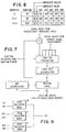
- For example, suppose a 15-input NOR gate is to be simulated. Assuming its inputs come from
locations 101 through 115, an appropriate instruction sequence is shown in the table of Fig. 6. - The first instruction in the table selects an immediate logical 0 as its sixth input. The other two use the previous instruction's output as the sixth input, so their immediate fields are irrelevant (indicated by Xs in the table). The functions shown (two ORs followed by a NOR) cause the last instruction's output to be the NOR of all 15 inputs.
- It is to be noted that no other instructions may intervene in a sequence of instructions computing a function of more than five inputs in this manner, since they would destroy the logic accumulator contents.
- This method of simulating extended functions corresponds to a functional decomposition that is easy to perform for the most common logic primitives: AND, OR, NAND, NOR, EXOR, etc. For those primitives, the decomposition needed follows directly from the associativity of AND, OR, and EXOR, e.g., the decomposition used in the fifteen input NOR example above was

- For more general functions, the needed decomposition is more difficult to find, if it exists at all. Simulation of such more general functions can be done in a straight-forward fashion by use of the logic simulation machine facilities for "dotted" logic presented in the next section.
- "Dotted" (or "wired", or "wired-tied") logic, performed in hardware by directly connecting gate outputs, can be simulated by use of logic unit elements labelled dotting logic and dot accumulator in Fig. 7. These elements are controlled by three flags in each instruction: the SAVE FOR DOT flag, the DOT SELECT flag, and the DOT FUNCTION flag.
- When SAVE FOR DOT is 1, the output of the logic unit for the instruction is stored in the dot accumulator. Otherwise, the instruction does not modify the Dot Accumulator.
- When DOT SELECT is 1, the output of the logic unit, which is the value stored in next signal value memory, is a function (AND or OR) of the current dot accumulator contents and the output of the current instruction (logic unit accumulator contents). This final value may be saved in the dot accumulator by using the SAVE FOR DOT flag.
- When the DOT SELECT flag is 0, the logic unit accumulator contents for the current instruction is stored directly into the next signal value memory. No interaction with the current contents of the dot accumulator occurs.
- DOT FUNCTION defines the "dotted logic" function performed: DOT FUNCTION=0 selects AND, and DOT FUNCT)ON=1 selects OR (assuming the convention that 00 is logical 0 and 10 is logical 1; the opposite convention reverses the DOT FUNCTION meanings). DOT FUNCTION is active only when DOT SELECT is 1.
- As an example, reference is made to Fig. 8, which shows a 3-way collector dot ("dotted OR"). The numbers near the gates are instruction memory addresses for instructions representing the gates; the numbers at the inputs are addresses of the input data, and the number at the output is the address where the final dotted result is placed in next signal value memory.
- The table of Fig. 9 shows instructions implementing the simulation of dotting for the example. Unused inputs have been left blank for clarity, and the immediate select and immediate value fields were left out also since they are not relevant to the example.
- The first instruction in the table just saves its result. Its DOT FUNCTION flag is immaterial (indicated by an X) since its DOT SELECT flag is 0. The second instruction ANDs its result with the saved first instruction's result and saves that. (Note that AND is used since the common term "wired OR" actually refers to the opposite logic convention). The third instruction also ANDs its result with the saved dotting result; its output is the final dotted logic result, so it does not save for further dotting.
- Note that several instructions can intervene between two whose outputs are to be "dotted" together, providing they do not alter the dot accumulator. This allows the simulation of "wired logic" between gates of more than five inputs.
- The dotted logic facilities of the logic simulation machine can also be used in simulating gates with more than 5 inputs. This is particularly useful for simulating gates implementing complex functions since a decomposition into product-of-sums or sum-of-products form can be the basis of the representation used. Individual instructions perform the first level of the decomposition (the several sums or products), and the dotting logic is used to perform the second level (the single outer level product or sum).
- It was previously stated that the order of instructions in the instruction memory was not relevant. This is clearly not true for sequences of instructions using the logic unit accumulator and dot accumulator. However, such seauences are typically needed only to simulate a small minoritv of a device's logic, and a sequence as a whole can be arbitrarily positioned in instruction memory.
- The primary function of the
inter-processor switch 33 of Fig. 1 is to communicate instruction results from the basic processors generating them to basic processors using them. That function will now be described. - The
inter-processor switch 33 connects all the basic processors 1-31 and thecontrol processor 32. This is illustrated in Fig. 1. - The communication of results between processors makes use of additional memories within each basic processor as shown in Fig. 1.
- The function of these memories in providing inter-processor communication through the switch is described below.
- As illustrated in Fig. 1, each basic processor has two additional internal logic data memories. These are identical to the current and next
signal value memories signal value memories signal input memory 38 and that of the nextsignal input memory 39. Their functions will be described in terms of these roles. The actual data memories have been called the A-IN memory and the B-IN memory. - Like the
signal value memories signal input memories - The data in current
signal input memory 38 are logic signal values that are currently present in the simulation, and were generated by other basic processors. This data is selected by use of ADDRESS SOURCE flags in each basic processor instruction. Each of the five addresses in an instruction has an associated ADDRESS SOURCE flag. When it is 0, the address references data in current signal value memory; when 1, the address references data in current signal input memory. Thus any or all of the data used in computing logic function can come from other processors. - In the course of a major cycle, updated values are obtained from the
inter-processor switch 33 and placed in the nextsignal input memory 39; and at the end of each major cycle, the former next signal input memory is designated to be the current signal input memory (and visa versa). - The switch
select memory 40 of each basic processor has 1024 locations, each containing the address of a basic processor. Theinter-processor switch 33 uses the switchselect memory 40 to place updated logic signal values in the nextsignal input memory 39 as follows: - The result of each instruction, the value stored in a basic processor's next
signal value memory 36, is always sent to theinter-processor switch 33 by every processor, as indicated in Fig. 1. Furthermore, the major and minor cycles (instruction executions) of all basic processors are synchronized: every basic processor executes its Kth instruction at the same time. Thus, all processor's results are sent to theinter-processor switch 33 simultaneously, in the order of their addresses in next and currentsignal value memories - The switch
select memory 40 and nextsignal input memory 39 are also stepped through in address order, synchronized with instruction execution. At each minor cycle, the switch sends to each basic processor the current output of the basic processor addressed by the current switchselect memory 40 location. This output is placed in the current location in nextsignal input memory 39. Thus, if a basic processor's switchselect memory 40 has Q in location Z, it receives the Zth output of basic processor Q; this is placed in location Z of its nextsignal input memory 39. - The tables shown in Figs. 11 and 12 show the switch
select memory 40 andinstruction memory 202 contents providing the required communication for the circuit shown in Fig. 10, assuming the allocation to processors shown in Fig. 12. The numbers in Fig. 12 are instruction/data locations corresponding to the gates and signal lines shown. Unused elements have been left out of the instructions for clarity. - Since
processor 3 needsProcessor 2's 49th output, the table of Fig. 11 shows a 2 inprocessor 3's 49th switch select memory location. This places the needed value inprocessor 3's 49th nextsignal input memory 39, so the table of Fig. 12 showsprocessor 3's 18th instruction accessing that location with its second address. The other table elements are derived similarly. It should be noted that atminor cycle 18,Processor 1 simultaneously transmits and receives, sending data toProcessors Processor 3. - Suppose a basic processor needs data generated in two other processors, and they generate it at the same minor cycle (same instruction location). The needed communication cannot be performed, since a basic processor can receive the output of only one other processor at each minor cycle.
- However, instruction execution order is arbitrary (except for extended functions and "dotted" logic), so instructions can be ordered in
instruction memory 202 to avoid such conflicts. The problem of discovering such an ordering is called the scheduling problem. - The scheduling problem must be solved by the logic simulation machine compiler for each device to be simulated. Just as physical components must be placed and wired, simulated logic must be partitioned among the processors and scheduled.
- Partitioning and scheduling is readily achieved in the logic simulation. Communication can be scheduled even when extremely simple partitioning is used, such as, placing the first N gates in
processor 1, the next N inprocessor 2, etc. Even examples containing substantial use of the logic accumulator may be successfully scheduled using this simple partitioning. - The
control processor 32 of the logic simulation machine provides two functions of particular interest, they are organizing signal values into functional groups so that they can read from or write into the logic simulation machine with a single local computer (51) input/output operation, and halting the logic simulation machine and interrupting the local computer when any of a group of selected signals are set to specified values. - The first function provides for efficient application of input sequences and gathering of data by the local computer. The halting function is the basic mechanism for informing the local computer of events in the simulation such as user-defined events or requests for array read or write. The control processor including these two functions are discussed as follows.
- The
control processor 32 contains two counters which are of use in controlling overall logic simulation machine execution. - The control processor also provides general logic simulation machine control function, such as, starting the logic simulation machine, halting it, etc. These are provided via commands from the local computer which utilize the control processor in a transparent manner.
- The control processor contains six memories referred to as a switch select memory, an output signal memory, an input signal memory, an output permutation memory, an input permutation memory, and an event mask.
- The characteristics and functions of each of these memories are described below.
- The switch select memory of the control processor and its connection to the
inter-processor switch 33 are identical in configuration and operation to switchselect memory 40 of a basic processor as shown in Fig. 1. Data is sent to theinter-processor switch 33 from thecontrol processor 32 each minor cycle; and the control processor's switch select memory determines the basic processor from which it receives data each minor cycle. - The input and output signal memories serve as a sink and a source, respectively, of logic data communicated between the
control processor 32 and the basic processors 1-31 via the inter-processor switch 33. Both has 1024 locations, each holding a single signal. - In contrast to other signal data memories in the logic simulation machine, no internal logic simulation machine action ever reads the contents of the input signal memory; it is read only into the local computer main storage.via its input/output operations. Similarly, no internal action ever alters the contents of the output signal memory; it is loaded only from the local computer main storage via its input/output operations. In addition, no swapping of these memories occurs between major cycles.
- The function of the input and output permutation memories is to permute the transmission order of values in the input and output signal memories respectively. Each of these memories contains 1024 locations of 10 bits each; an address in the associated signal memory is contained in each location.
- Every major cycle, the input permutation memory is cycled through in address order, synchronized with basic processor instruction execution. The address in the current input permutation memory location is used as the address in input signal memory where data currently received from the inter- processor switch is placed. The output permutation memory is cycled through in the same manner. The contents of each location is used as the address in the output signal memory from which data is sent to the
interprocessor switch 33. - This permutation of signal order allows data to be functionally grouped in the output signal memory, minimizing the local computer input/output operations needed to alter it. Such functional grouping might otherwise be impossible to achieve, due to the requirements of scheduling inter- processor data transfers through the
inter-processor switch 33. For example, a set of test inputs can be positioned in contiguous locations of the output signal memory and stored there with a single local computer input/output operation; appropriate output permutation memory contents can then feed that data to the switch at the minor cycles to which they have been scheduled for conflict-free inter- processor communication. - The event mask in
control processor 32 allows the logic simulation machine to halt in response to events in the simulation itself, i.e., the setting of some simulated signal(s) to selected value(s). - The event mask contains 1024 locations of 4 bits each. Each of the bits corresponds to an individual value of the 2-bit code for simulated signal values: the first bit corresponds to 00, the second to 01, the third to 10, and the last to 11.
- The event mask, in parallel with the output and input permutation memories of
control processor 32, is cycled through in address order as part of a major cycle. As each signal value is received from theinter-processor switch 33, it is matched against the contents of the current event mask location. If the location contains a "1" corresponding to the signal value, the simulator is halted at the end of the current major cycle and an interrupt is presented to the local computer. - It should be noted that event mask locations correspond to signal values in the order they are received from the switch, not in the (permuted) order of storage in input signal memory.
- Since the event mask can have more than a single "1" " in each location, any of several values of a particular signal can be made to cause the simulator to halt. For example, the simulator could be halted when a particular signal is set to anything except logical 0.
- Since the logic simulation machine only halts at the end of a major cycle, thus ensuring consistency of all simulated signal values, more than one signal value can match the event mask settings before the halt and interrupt, effectively causing a halt for several reasons simultaneously. For this reason, the local computer is given no direct indication as to which signal value caused the halt. Instead, controlling software in the local computer must read the contents of the input signal memory to determine which signal value(s) caused the halt. This implies another use of the output permutation memory: all the simulated signal values which could cause a halt can be grouped in input signal memory and thus read by a single local computer input/output operation.
- The control processor also contains two identical counters called
level counter 1 andlevel counter 2, each 16 bits long. They can be loaded via local computer input/output commands, and are decremented each major cycle. When either reaches 0, the local computer is interrupted. - These counters can be used for various purposes. For example, one can count the major cycles (gate delays) per logic cycle of the simulated device, giving the local computer an interrupt when it is time to gather an output vector and apply a new input vector. The other can count the total number of major cycles a simulation is to run.
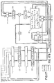
- A more detailed description of the
logic simulation machine 50 shown in block diagram form in Fig. 1 will now be provided. Figs. 13A, 13B, 13C, 13D and 13E can be arranged as shown in Fig. 13. Figs. 13A, 13B, 13C and 13D illustrate the entire logic simulation machine and Fig. 13E is an illustration of waveforms used in the description of Figs. 13A through 13D. - Referring to Figs. 13A and 13B, and as previously stated, there are thirty-one processors numbered from
number 1 tonumber 31 as also shown in Fig. 1.Processor number 31 is shown in diagrammatic form on Figs. 13A and 13B. - Also as previously stated, the actual number of the just mentioned processors is not important. There could be more processors or less. The number of thirty processors is chosen as one example of a practical machine embodiment of the invention. In addition to the
processors number 1 through 31, there iscontrol processor 32 also shown in Fig. 1, which is shown on Fig. 13C and 13D.Control processor 32 will be described in detail later and as previously stated is used mainly to accumulate the result and to provide the control pulses which are needed for the entire logic simulation machine of this embodiment. - In Fig. 13A, the
address counter 200, is used to supply addresses to theinstruction memory 202. In the present embodiment, theinstruction memory 202 has provisions for 1024 words. This number is only used as an example, and a greater or lesser number of words may be used. Actually, in the operation of the described machine, the total number of 1024 words in theinstruction memory 202 may not be used as will be understood in the later description. - From the
instruction memory 202, words are read into theinstruction register 204. Because of the pipelined structure of the machine, asecond instruction register 206 is needed into which the same word is read by the P-2 gate pulse also illustrated in Fig. 13E. Theregister 206 then acts as an input register to the "logic unit memory" 208 and to the memories labelled A, B, A IN and B IN. The left hand section ofregister 206 holds five operand addresses. The middle section of this register holds some control bits and the right-hand portion hold the operation code. The operation code in the right-hand portion ofregister 206 acts as an address to the logic unit memory to place a word in the "logic unit memory register" section ofregister 210. The control section is passed fromregister 206 to register 210 by the P-1 gate pulse which is also shown in Fig. 13E. The A and B memories and their sections A IN and B IN are special memories and will be described more in detail later. At this point in the description, it can be mentioned that either the A and A IN or the B and B IN memories can be read and placed in the "logic unit input register" ofregister 210. As previously described, and as will be explained in more detail later, there are "minor cycles" and "major cycles" in the logic simulation machine operation. During a "minor cycle" one instruction in theinstruction memory 202 on Fig. 13A is read and processed. A "major cycle" can consist of 1024 of these "minor cycles". The function of the A, B, A IN and B IN memories is that they are used alternately. For example, during one major cycle the A and A IN memories may be read. - In the next "major cycle" the B and B IN memories will be read. The switching between the A and A IN and the B and B IN memories is accomplished by the switching mechanism indicated by the dotted
line 212 on Fig. 13A. If it be assumed that, in a certain major cycle, the A and A IN memories are read out of in this same major cycle, the B and B IN memories can be read into. When the A and A IN memories are read out of, these two memories are regarded as a single memory. The A and the A IN are both memories addressed by the low order ten bits of the operand inregister 206 while the high order bit of this same operand selects which of the two (A or A IN) memories is actually read. In other words, the operands inregister 206 are eleven bits. When the A, A IN, B or B IN memories are written into, each one of these memories are regarded as separate memories and are both addressed by ten bits which is contained in theaddress register 214 on Fig. 13A. These memories will be described in much more detail later on in the description. - Referring again to Fig. 13A, information in
register 210 is transferred to register 216 by the P-2 gate pulse. This permits the information inregister 216 to be applied to the "logic unit first step" 218 which will be described in more detail later. The output of the "logic unit first step" 218 and also the control bits number "1 1 ", "12" and "13" are transferred to 220 on Fig. 13B by the P-1 gate pulse. Fromregister 220 these data are gated to register 222 by the gate pulse P-2.Register 222 serves as the input register for the "logic unit second step" 224. The "logic unit second step" 224 will be described in more detail later. From this unit, the results are gated to the logicunit output register 226 by the pulse P-1. - From
register 226, information is gated to register 228 by the P-2 gate pulse. These delay registers are necessary in the machine because of the "pipelining" used in the design. Fromregister 228 it can be seen that data has two paths. One is back to the processor viacable 230 so that information can be written into either the A or B memories according to the setting of the switches represented byreference character 212. The other path for data is viacable 232 which goes to the interprocessor switch. Depending on the setting of the gates in theinter-processor switch 33 shown in Fig. 1, information can be gated from any processor back to itself or to any other processor in the group fromprocessor number 1 throughprocessor number 32. When this information comes in from theinter-processor switch 33 it always goes into either the A IN or the B IN memories. Theinter-processor switch 33 will be described in more detail later. - Reference should next be made to Figs. 13C and 13D for the description of the
control processor 32.Control processor number 32 permutes and accumulates information produced by other thirty-one processors, keeps track of "events" and contains all the pulse generation equipment used to control the whole machine of this embodiment. On Fig. 13C, the "address counter" 234 is used to address the "permuter instruction memory" 236 which again can contain up to 1024 words. This memory is read by the P-1 gate pulse and the memory word is placed in theregister 238. Fromregister 238 the information is gated to register 240 by the P-2 gate pulse.Register 240 controls the reading and writing of the A and A IN memories and also provides an input to the "event logic" which is shown in detail on Fig. 18. - The A and A IN memories are used differently in
processor number 32 than in the other thirty-one processors. The data is always read out of memory A and goes bycable 242 to the inter-processor switch. The data from the switch is written into memory A IN. On Fig. 13C, it will be noted that data coming in from theinter-processor switch 33 oncable 244 is not only applied to the memories but also serves as an input to the event logic. - Referring to the right side of Fig. 13D, the logic simulation machine of this embodiment is started by a "start" pulse applied to the
lead 246. This pulse extends through the ORcircuit 248 to turn "on"single shot device 250. - This produces the CL-1 pulse shown in Fig. 13E which is used to reset the address counters and to trigger the "swap" switch. The "swap" switch is used to switch the A and B memories in the various processors. The CL-1 pulse is also used to set the "event latch" 260 to its "0" state and also to reset to "0" the "count up counter" 264. After the CL-1 pulse disappears, the
delay circuit 252 will have an output to turn "on"single shot device 254 in order to produce the CL-2 pulse. The CL-2 pulse sets theflip flop 256 to its "1" state thus turning on the pulse generator 258. The pulse generator 258 produces the P-1, P-2 and P-3 gate pulses in succession as shown by the timing chart of Fig. 13E. The P-1 and P-2 gate pulses are used to step the pipeline of the machine. The P-3 gate pulse is used to test the output of the compareunit 266. The "total count register" 268 is initially set for the total number of minor cycles required. - A "minor" cycle can be considered to be a time required to produce a single train of three gate pulses, in other words the time to produce a single train consisting of P-1 gate pulse, a P-2 gate pulse and a P-3 gate pulse. The "total count register" 268 is set to a number which is equal to the total number of "minor" cycles plus the number of cycles required to run the last data through the pipeline. The "count up counter" 264 is incremented each "minor" cycle by the P-1 gate pulse. When the "count up counter" 264 is equal to the "total count register" 268, a pulse will be produced by the "compare unit" 266 which extends to the AND
circuit 270 which is tested each "minor" cycle by the P-3 gate pulse. The pulse produced by the ANDcircuit 270 at this time extends theflip flop device 256 to reset it to its "0" state thus turning off the pulse generator 258. The same pulse is also applied togate 262 in order to test "event latch" 260. If thelatch 260 is still on its "0" state, a pulse will be produced onwire 272, which extends through ORcircuit 248 to again turn "on"single shot device 250 in order to start a new major cycle. If the "event latch" 260 is in its "1" state, a pulse will appear onlead 274 to signal the end of operations. This timing chart of Fig. 13E will be understood better when the detailed circuits shown in the remaining figures are described. - Reference should next be made to Figs. 14A and 14B (arranged as illustrated in Fig. 14) which show the detailed circuitry for the A, B, A IN and B IN memories. These are the memories shown on the right portion of Fig. 13A. These memories are grouped into five groups of four each. One group is shown in detail on Fig. 14A. Each memory has a capacity of 1024 words and each word is two bits long. In the beginning, before the logic simulation machine is started, all memories are loaded with initialized data.
- The five operand addresses existing in the
register 206 on Fig. 13A are fed to the five memory sections in Fig. 13A and therefore, five stored values are presented to register 210 on Fig. 13A each time a read-access is performed on the memories. Depending on the setting of theswitch 276 at the left side of Fig. 14A, the memories A or A IN will be read or the memories B or B IN will be read. At this point, it is important to note that the A or A IN memories or the B or B IN memories are read as a single memory. - The low order ten bits of the operand section of the
register 206 are used to address both A and A IN or both B and B IN. The high order bit or the eleventh bit of this operand section is used to select either the normal or the IN sections. The important consideration at this point is that when these memories are read, the A and the A IN memories or the B and the B IN memories are read as a single unit. This is not true when the memories are written into as will be described later. When these just mentioned memories are written into, tney are addressed separately by theaddress counter 214 shown at the upper left of Fig. 14A which has only ten bits. The switches represented by thereference character 212 on Fig. 13A, are shown on Fig. 14A by thegates switch 276. Ifswitch 276 is in its "0" position, thegates 278 and 284 will be enabled thus permitting the memories A or A IN to be read out of and the memories B and B IN be written into. - The read and write pulses are applied to the memories on Fig. 14A by the P-1 pulse through gate 286.
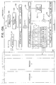
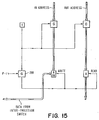
- Reference should next be made to Fig. 15 which shows the A and A IN memories for the
control processor number 32. These memories are similar to those in the other processors except that they are used in a much simpler manner. Information is always read out of the A memory and always written into the A IN memory. Reading and writing of the memory is done by the P-1 pulse which is applied to thegate 288. - Reference should next be made to Figs. 16A and 16B, arranged as shown in Fig. 16 which is a detail of the inter-processor switch which is indicated in Fig. 1 and by the dotted lines on the left side of Figs. 13A and 13D. The inter-processor switch has its
own address counter 290 which supplies addresses to theswitch memory 292. Memory words are placed into theregister 294 by the P-1 gate pulse and later transferred to register 296 by the P-2 gate pulse. There are thirty-two sections of the five bits each inregister 296 and each one of these sections is decoded into one of thirty-two leads. The groups of leads from each one of these decoders is applied to gates such as 298, 300, 302 and 304. These gates are pulsed each "minor" cycle by the P-1 gate pulse. In this manner, pulses appear on cables such as 306, 308, 310 and 312 to enable gates such as 314, 316 through 318 and 320. An examination of the cables and the gates on Fig. 16 will indicate that data coming from any processor can be gated to itself or to any other processor by the P-1 gate pulse. It is believed that the operation of the inter-processor switch may now be understood by one skilled in the art and that no further explanation is needed for Figs. 16A and 16B. - Reference should next be made to Figs. 17A and 17B arranged as illustrated in Fig. 17. Fig. 17A shows how the information in the
register 216, which is also shown on Fig. 13B, refers to the logic unit for step one and how the control bits are directed to gates which suitably control the logic. From Fig. 17A, the results of the logic unit first step are passed along with certain of the control bits in register 216 (Fig. 13B) to the logic unit second step shown in Fig. 17B. The Boolean logic equations for the logic unit second step are shown in Fig. 17B and it is believed that there will be no difficulty in understanding the operation of this unit. - The "logic unit first step" shown in Fig. 17A carries out specific logic functions. The inputs to "logic unit first step" accepts


- Using the a, a', b, b' ... e' so produced then the logic performs the following operations:


- Using the FP values thus generated and the


- And then, using the above values:

- Finally, reference is made to Fig. 18 which shows the details of event logic of Fig. 13C. The event logic is shown on Fig. 13C with one of its inputs coming from the mask field in
register 240 and its input from thecable 244 which comes from the inter-processor switch. As shown on Fig. 18, the data from the mask field inregister 240 combines with the data from the inter-processor switch to produce an output of theOR circuit 322 which provides an output online 324 in order to set the "event latch" 260 to its "1" state. Then, it is said that an "event" has occurred. As mentioned before, the detection of an "event" causes a signal to appear onlead wire 274 on Fig. 13D which signals the end of operations. - In other words, no more major cycles are needed. The results of the operations now existing in the A, B, A IN or B IN memories in
processor numbers 1 through 31 and the A IN memory inprocessor 32 can be analyzed in any suitable manner. Such analyzing of this data in the machine to be built will be done by thehost computer 52 in conjunction with thelocal computer 51 which acts as an interface between the host computer and thelogic simulation machine 50.
Claims (6)
Applications Claiming Priority (2)
| Application Number | Priority Date | Filing Date | Title |
|---|---|---|---|
| US53444 | 1979-06-29 | ||
| US06/053,444 US4306286A (en) | 1979-06-29 | 1979-06-29 | Logic simulation machine |
Publications (2)
| Publication Number | Publication Date |
|---|---|
| EP0021404A1 EP0021404A1 (en) | 1981-01-07 |
| EP0021404B1 true EP0021404B1 (en) | 1983-05-11 |
Family
ID=21984277
Family Applications (1)
| Application Number | Title | Priority Date | Filing Date |
|---|---|---|---|
| EP80103561A Expired EP0021404B1 (en) | 1979-06-29 | 1980-06-24 | Computing system for the simulation of logic operations |
Country Status (5)
| Country | Link |
|---|---|
| US (1) | US4306286A (en) |
| EP (1) | EP0021404B1 (en) |
| JP (1) | JPS5948424B2 (en) |
| DE (1) | DE3063100D1 (en) |
| IT (1) | IT1150956B (en) |
Families Citing this family (154)
| Publication number | Priority date | Publication date | Assignee | Title |
|---|---|---|---|---|
| JPS57212508A (en) * | 1981-06-25 | 1982-12-27 | Mitsubishi Electric Corp | Programming device with cathode ray tube |
| JPS5814257A (en) * | 1981-07-17 | 1983-01-27 | Fujitsu Ltd | Data processor for logical simulation |
| JPS58146947A (en) * | 1982-02-26 | 1983-09-01 | Nec Corp | Logical simulator |
| DE3221819A1 (en) * | 1982-06-09 | 1984-02-23 | Siemens AG, 1000 Berlin und 8000 München | Device for simulating a switching device with the aid of a computer |
| US4656580A (en) * | 1982-06-11 | 1987-04-07 | International Business Machines Corporation | Logic simulation machine |
| EP0099114B1 (en) * | 1982-07-13 | 1988-05-11 | Nec Corporation | Logic simulator operable on level basis and on logic block basis on each level |
| JPS5975347A (en) * | 1982-10-21 | 1984-04-28 | Toshiba Corp | Simulation device of logical circuit |
| US4527249A (en) * | 1982-10-22 | 1985-07-02 | Control Data Corporation | Simulator system for logic design validation |
| US4587625A (en) * | 1983-07-05 | 1986-05-06 | Motorola Inc. | Processor for simulating digital structures |
| WO1985002033A1 (en) * | 1983-11-03 | 1985-05-09 | Prime Computer, Inc. | Digital system simulation method and apparatus |
| US4628471A (en) * | 1984-02-02 | 1986-12-09 | Prime Computer, Inc. | Digital system simulation method and apparatus having two signal-level modes of operation |
| US4814983A (en) * | 1984-03-28 | 1989-03-21 | Daisy Systems Corporation | Digital computer for implementing event driven simulation algorithm |
| US4751637A (en) * | 1984-03-28 | 1988-06-14 | Daisy Systems Corporation | Digital computer for implementing event driven simulation algorithm |
| US4777618A (en) * | 1984-07-19 | 1988-10-11 | Nippondenso Co., Ltd. | Method of storing, indicating or producing signals and apparatus for recording or producing signals |
| JPS6142040A (en) * | 1984-08-03 | 1986-02-28 | Nec Corp | Logical simulator |
| JPS6165336A (en) * | 1984-09-07 | 1986-04-03 | Hitachi Ltd | High-speed arithmetic system |
| JPS61102569A (en) * | 1984-10-26 | 1986-05-21 | Hitachi Ltd | Fast logical simultation device |
| US4819150A (en) * | 1985-04-05 | 1989-04-04 | Unisys Corporation | Array for simulating computer functions for large computer systems |
| JPH0743733B2 (en) * | 1985-12-11 | 1995-05-15 | 株式会社日立製作所 | Logical simulation method |
| US5036453A (en) * | 1985-12-12 | 1991-07-30 | Texas Instruments Incorporated | Master/slave sequencing processor |
| US4763289A (en) * | 1985-12-31 | 1988-08-09 | International Business Machines Corporation | Method for the modeling and fault simulation of complementary metal oxide semiconductor circuits |
| US4937770A (en) * | 1986-02-07 | 1990-06-26 | Teradyne, Inc. | Simulation system |
| US4744084A (en) * | 1986-02-27 | 1988-05-10 | Mentor Graphics Corporation | Hardware modeling system and method for simulating portions of electrical circuits |
| US4792909A (en) * | 1986-04-07 | 1988-12-20 | Xerox Corporation | Boolean logic layout generator |
| US4862347A (en) * | 1986-04-22 | 1989-08-29 | International Business Machine Corporation | System for simulating memory arrays in a logic simulation machine |
| JPS62251843A (en) * | 1986-04-25 | 1987-11-02 | Hitachi Ltd | Logical simulation method and its apparatus |
| US5126966A (en) * | 1986-06-25 | 1992-06-30 | Ikos Systems, Inc. | High speed logic simulation system with stimulus engine using independent event channels selectively driven by independent stimulus programs |
| US4787061A (en) * | 1986-06-25 | 1988-11-22 | Ikos Systems, Inc. | Dual delay mode pipelined logic simulator |
| US4787062A (en) * | 1986-06-26 | 1988-11-22 | Ikos Systems, Inc. | Glitch detection by forcing the output of a simulated logic device to an undefined state |
| US4821173A (en) * | 1986-06-30 | 1989-04-11 | Motorola, Inc. | Wired "OR" bus evaluator for logic simulation |
| US4815016A (en) * | 1986-07-24 | 1989-03-21 | Unisys Corp. | High speed logical circuit simulator |
| US4827427A (en) * | 1987-03-05 | 1989-05-02 | Hyduke Stanley M | Instantaneous incremental compiler for producing logic circuit designs |
| US5257201A (en) * | 1987-03-20 | 1993-10-26 | International Business Machines Corporation | Method to efficiently reduce the number of connections in a circuit |
| US4816999A (en) * | 1987-05-20 | 1989-03-28 | International Business Machines Corporation | Method of detecting constants and removing redundant connections in a logic network |
| US4873656A (en) * | 1987-06-26 | 1989-10-10 | Daisy Systems Corporation | Multiple processor accelerator for logic simulation |
| US4916647A (en) * | 1987-06-26 | 1990-04-10 | Daisy Systems Corporation | Hardwired pipeline processor for logic simulation |
| US4872125A (en) * | 1987-06-26 | 1989-10-03 | Daisy Systems Corporation | Multiple processor accelerator for logic simulation |
| US4914612A (en) * | 1988-03-31 | 1990-04-03 | International Business Machines Corporation | Massively distributed simulation engine |
| US4989131A (en) * | 1988-07-26 | 1991-01-29 | International Business Machines Corporation | Technique for parallel synchronization |
| US5452231A (en) * | 1988-10-05 | 1995-09-19 | Quickturn Design Systems, Inc. | Hierarchically connected reconfigurable logic assembly |
| US5109353A (en) * | 1988-12-02 | 1992-04-28 | Quickturn Systems, Incorporated | Apparatus for emulation of electronic hardware system |
| US5329470A (en) * | 1988-12-02 | 1994-07-12 | Quickturn Systems, Inc. | Reconfigurable hardware emulation system |
| US5572708A (en) * | 1989-02-28 | 1996-11-05 | Nec Corporation | Hardware simulator capable of dealing with a description of a functional level |
| US5369593A (en) * | 1989-05-31 | 1994-11-29 | Synopsys Inc. | System for and method of connecting a hardware modeling element to a hardware modeling system |
| US5353243A (en) * | 1989-05-31 | 1994-10-04 | Synopsys Inc. | Hardware modeling system and method of use |
| US5091872A (en) * | 1989-06-23 | 1992-02-25 | At&T Bell Laboratories | Apparatus and method for performing spike analysis in a logic simulator |
| KR0158887B1 (en) * | 1990-01-12 | 1999-02-18 | 이노우에 키요시 | Logie simmulator |
| US5375074A (en) * | 1990-01-23 | 1994-12-20 | At&T Corp. | Unboundedly parallel simulations |
| US5161156A (en) * | 1990-02-02 | 1992-11-03 | International Business Machines Corporation | Multiprocessing packet switching connection system having provision for error correction and recovery |
| EP0445454B1 (en) * | 1990-03-08 | 1997-06-18 | International Business Machines Corporation | Hardware simulator |
| JPH05205005A (en) * | 1990-03-30 | 1993-08-13 | Internatl Business Mach Corp <Ibm> | Host-interface for logic-simulation-machine |
| US5327361A (en) * | 1990-03-30 | 1994-07-05 | International Business Machines Corporation | Events trace gatherer for a logic simulation machine |
| JPH04116779A (en) * | 1990-09-07 | 1992-04-17 | Takayama:Kk | Data processor |
| US5291612A (en) * | 1991-02-11 | 1994-03-01 | University Technologies International | System for evaluating boolean expressions using total differential generating tree structured processing elements controlled by partial subfunction differentials |
| US5257266A (en) * | 1991-02-27 | 1993-10-26 | General Dynamics Corporation, Space Systems Division | Computer and communications systems employing universal direct spherics processing architectures |
| US5442772A (en) * | 1991-03-29 | 1995-08-15 | International Business Machines Corporation | Common breakpoint in virtual time logic simulation for parallel processors |
| EP0508619A2 (en) * | 1991-04-11 | 1992-10-14 | Hewlett-Packard Company | Bi-directional socket stimulus interface for a logic simulator |
| GB9121540D0 (en) * | 1991-10-10 | 1991-11-27 | Smiths Industries Plc | Computing systems and methods |
| US5475830A (en) * | 1992-01-31 | 1995-12-12 | Quickturn Design Systems, Inc. | Structure and method for providing a reconfigurable emulation circuit without hold time violations |
| US5425036A (en) * | 1992-09-18 | 1995-06-13 | Quickturn Design Systems, Inc. | Method and apparatus for debugging reconfigurable emulation systems |
| US5452239A (en) * | 1993-01-29 | 1995-09-19 | Quickturn Design Systems, Inc. | Method of removing gated clocks from the clock nets of a netlist for timing sensitive implementation of the netlist in a hardware emulation system |
| US5594741A (en) * | 1993-03-31 | 1997-01-14 | Digital Equipment Corporation | Method for control of random test vector generation |
| IL109921A (en) * | 1993-06-24 | 1997-09-30 | Quickturn Design Systems | Method and apparatus for configuring memory circuits |
| JP3083220B2 (en) * | 1993-08-09 | 2000-09-04 | 株式会社日立製作所 | Design support system |
| US5680583A (en) * | 1994-02-16 | 1997-10-21 | Arkos Design, Inc. | Method and apparatus for a trace buffer in an emulation system |
| US5495419A (en) * | 1994-04-19 | 1996-02-27 | Lsi Logic Corporation | Integrated circuit physical design automation system utilizing optimization process decomposition and parallel processing |
| US5557533A (en) * | 1994-04-19 | 1996-09-17 | Lsi Logic Corporation | Cell placement alteration apparatus for integrated circuit chip physical design automation system |
| US6155725A (en) * | 1994-04-19 | 2000-12-05 | Lsi Logic Corporation | Cell placement representation and transposition for integrated circuit physical design automation system |
| US5963975A (en) * | 1994-04-19 | 1999-10-05 | Lsi Logic Corporation | Single chip integrated circuit distributed shared memory (DSM) and communications nodes |
| US5914887A (en) * | 1994-04-19 | 1999-06-22 | Lsi Logic Corporation | Congestion based cost factor computing apparatus for integrated circuit physical design automation system |
| US5875117A (en) * | 1994-04-19 | 1999-02-23 | Lsi Logic Corporation | Simultaneous placement and routing (SPAR) method for integrated circuit physical design automation system |
| US5815403A (en) * | 1994-04-19 | 1998-09-29 | Lsi Logic Corporation | Fail-safe distributive processing method for producing a highest fitness cell placement for an integrated circuit chip |
| US6493658B1 (en) | 1994-04-19 | 2002-12-10 | Lsi Logic Corporation | Optimization processing for integrated circuit physical design automation system using optimally switched fitness improvement algorithms |
| US5559718A (en) * | 1994-04-28 | 1996-09-24 | Cadence Design Systems, Inc. | System and method for model-based verification of local design rules |
| US5920712A (en) * | 1994-05-13 | 1999-07-06 | Quickturn Design Systems, Inc. | Emulation system having multiple emulator clock cycles per emulated clock cycle |
| US5551013A (en) * | 1994-06-03 | 1996-08-27 | International Business Machines Corporation | Multiprocessor for hardware emulation |
| US6208954B1 (en) * | 1994-09-16 | 2001-03-27 | Wind River Systems, Inc. | Method for scheduling event sequences |
| US5615127A (en) * | 1994-11-30 | 1997-03-25 | International Business Machines Corporation | Parallel execution of a complex task partitioned into a plurality of entities |
| GB2296619B (en) * | 1994-12-20 | 1998-12-16 | Northern Telecom Ltd | Network emulation tool |
| US5649164A (en) * | 1994-12-30 | 1997-07-15 | International Business Machines Corporation | Sets and holds in virtual time logic simulation for parallel processors |
| US5546562A (en) * | 1995-02-28 | 1996-08-13 | Patel; Chandresh | Method and apparatus to emulate VLSI circuits within a logic simulator |
| US5632028A (en) * | 1995-03-03 | 1997-05-20 | Hal Computer Systems, Inc. | Hardware support for fast software emulation of unimplemented instructions |
| JP3242277B2 (en) * | 1995-03-20 | 2001-12-25 | 富士通株式会社 | Simulation equipment |
| US5706476A (en) * | 1995-06-05 | 1998-01-06 | Synopsys, Inc. | Method and apparatus for use of the undefined logic state and mixed multiple-state abstractions in digital logic simulation |
| US5923865A (en) * | 1995-06-28 | 1999-07-13 | Quickturn Design Systems, Inc. | Emulation system having multiple emulated clock cycles per emulator clock cycle and improved signal routing |
| US5819065A (en) * | 1995-06-28 | 1998-10-06 | Quickturn Design Systems, Inc. | System and method for emulating memory |
| US5819063A (en) * | 1995-09-11 | 1998-10-06 | International Business Machines Corporation | Method and data processing system for emulating a program |
| JP3645346B2 (en) * | 1996-01-22 | 2005-05-11 | 富士通株式会社 | Logic simulation device |
| US5868575A (en) * | 1996-05-20 | 1999-02-09 | Kuczewski; Robert M. | Cooperative/interactive learning system for logic instruction |
| US5822564A (en) * | 1996-06-03 | 1998-10-13 | Quickturn Design Systems, Inc. | Checkpointing in an emulation system |
| US6085032A (en) * | 1996-06-28 | 2000-07-04 | Lsi Logic Corporation | Advanced modular cell placement system with sinusoidal optimization |
| US5808899A (en) * | 1996-06-28 | 1998-09-15 | Lsi Logic Corporation | Advanced modular cell placement system with cell placement crystallization |
| US5963455A (en) * | 1996-06-28 | 1999-10-05 | Lsi Logic Corporation | Advanced modular cell placement system with functional sieve optimization technique |
| US6067409A (en) * | 1996-06-28 | 2000-05-23 | Lsi Logic Corporation | Advanced modular cell placement system |
| US5867398A (en) * | 1996-06-28 | 1999-02-02 | Lsi Logic Corporation | Advanced modular cell placement system with density driven capacity penalty system |
| US5812740A (en) * | 1996-06-28 | 1998-09-22 | Lsi Logic Corporation | Advanced modular cell placement system with neighborhood system driven optimization |
| US5835381A (en) * | 1996-06-28 | 1998-11-10 | Lsi Logic Corporation | Advanced modular cell placement system with minimizing maximal cut driven affinity system |
| US5831863A (en) * | 1996-06-28 | 1998-11-03 | Lsi Logic Corporation | Advanced modular cell placement system with wire length driven affinity system |
| US5872718A (en) * | 1996-06-28 | 1999-02-16 | Lsi Logic Corporation | Advanced modular cell placement system |
| US5914888A (en) * | 1996-06-28 | 1999-06-22 | Lsi Logic Corporation | Advanced modular cell placement system with coarse overflow remover |
| US5870311A (en) * | 1996-06-28 | 1999-02-09 | Lsi Logic Corporation | Advanced modular cell placement system with fast procedure for finding a levelizing cut point |
| US6026223A (en) * | 1996-06-28 | 2000-02-15 | Scepanovic; Ranko | Advanced modular cell placement system with overlap remover with minimal noise |
| US6030110A (en) * | 1996-06-28 | 2000-02-29 | Lsi Logic Corporation | Advanced modular cell placement system with median control and increase in resolution |
| US5844811A (en) * | 1996-06-28 | 1998-12-01 | Lsi Logic Corporation | Advanced modular cell placement system with universal affinity driven discrete placement optimization |
| US5892688A (en) * | 1996-06-28 | 1999-04-06 | Lsi Logic Corporation | Advanced modular cell placement system with iterative one dimensional preplacement optimization |
| US5870312A (en) * | 1996-06-28 | 1999-02-09 | Lsi Logic Corporation | Advanced modular cell placement system with dispersion-driven levelizing system |
| US5959993A (en) * | 1996-09-13 | 1999-09-28 | Lsi Logic Corporation | Scheduler design for ATM switches, and its implementation in a distributed shared memory architecture |
| US5831980A (en) * | 1996-09-13 | 1998-11-03 | Lsi Logic Corporation | Shared memory fabric architecture for very high speed ATM switches |
| US5886904A (en) * | 1996-09-23 | 1999-03-23 | Quickturn Design Systems, Inc. | Latch optimization in hardware logic emulation systems |
| US5841967A (en) * | 1996-10-17 | 1998-11-24 | Quickturn Design Systems, Inc. | Method and apparatus for design verification using emulation and simulation |
| US5980093A (en) * | 1996-12-04 | 1999-11-09 | Lsi Logic Corporation | Integrated circuit layout routing using multiprocessing |
| US5920485A (en) * | 1996-12-05 | 1999-07-06 | Hewlett-Packard | Method of selecting gates for efficient code generation by a circuit compiler |
| US6141636A (en) * | 1997-03-31 | 2000-10-31 | Quickturn Design Systems, Inc. | Logic analysis subsystem in a time-sliced emulator |
| US6321366B1 (en) | 1997-05-02 | 2001-11-20 | Axis Systems, Inc. | Timing-insensitive glitch-free logic system and method |
| US6009256A (en) * | 1997-05-02 | 1999-12-28 | Axis Systems, Inc. | Simulation/emulation system and method |
| US6421251B1 (en) | 1997-05-02 | 2002-07-16 | Axis Systems Inc | Array board interconnect system and method |
| US6134516A (en) * | 1997-05-02 | 2000-10-17 | Axis Systems, Inc. | Simulation server system and method |
| US6026230A (en) * | 1997-05-02 | 2000-02-15 | Axis Systems, Inc. | Memory simulation system and method |
| US6389379B1 (en) | 1997-05-02 | 2002-05-14 | Axis Systems, Inc. | Converification system and method |
| US5960191A (en) | 1997-05-30 | 1999-09-28 | Quickturn Design Systems, Inc. | Emulation system with time-multiplexed interconnect |
| US5970240A (en) * | 1997-06-25 | 1999-10-19 | Quickturn Design Systems, Inc. | Method and apparatus for configurable memory emulation |
| US6266802B1 (en) | 1997-10-27 | 2001-07-24 | International Business Machines Corporation | Detailed grid point layout using a massively parallel logic including an emulator/simulator paradigm |
| US6016563A (en) * | 1997-12-30 | 2000-01-18 | Fleisher; Evgeny G. | Method and apparatus for testing a logic design of a programmable logic device |
| US6279146B1 (en) | 1999-01-06 | 2001-08-21 | Simutech Corporation | Apparatus and method for verifying a multi-component electronic design |
| US6832182B1 (en) | 1999-04-08 | 2004-12-14 | Transim Technology Corporation | Circuit simulator |
| US6618698B1 (en) | 1999-08-12 | 2003-09-09 | Quickturn Design Systems, Inc. | Clustered processors in an emulation engine |
| US7356786B2 (en) | 1999-11-30 | 2008-04-08 | Synplicity, Inc. | Method and user interface for debugging an electronic system |
| US6823497B2 (en) | 1999-11-30 | 2004-11-23 | Synplicity, Inc. | Method and user interface for debugging an electronic system |
| US6931572B1 (en) | 1999-11-30 | 2005-08-16 | Synplicity, Inc. | Design instrumentation circuitry |
| US7065481B2 (en) | 1999-11-30 | 2006-06-20 | Synplicity, Inc. | Method and system for debugging an electronic system using instrumentation circuitry and a logic analyzer |
| US7072818B1 (en) | 1999-11-30 | 2006-07-04 | Synplicity, Inc. | Method and system for debugging an electronic system |
| US6581191B1 (en) | 1999-11-30 | 2003-06-17 | Synplicity, Inc. | Hardware debugging in a hardware description language |
| US6578133B1 (en) * | 2000-02-24 | 2003-06-10 | Stanley M. Hyduke | MIMD array of single bit processors for processing logic equations in strict sequential order |
| US7222315B2 (en) | 2000-11-28 | 2007-05-22 | Synplicity, Inc. | Hardware-based HDL code coverage and design analysis |
| US6898562B2 (en) | 2000-12-07 | 2005-05-24 | International Business Machines Corporation | Method and system for efficiently overriding net values in a logic simulator machine |
| US20030149962A1 (en) * | 2001-11-21 | 2003-08-07 | Willis John Christopher | Simulation of designs using programmable processors and electronically re-configurable logic arrays |
| US7328195B2 (en) * | 2001-11-21 | 2008-02-05 | Ftl Systems, Inc. | Semi-automatic generation of behavior models continuous value using iterative probing of a device or existing component model |
| US7260794B2 (en) * | 2002-12-20 | 2007-08-21 | Quickturn Design Systems, Inc. | Logic multiprocessor for FPGA implementation |
| US7698118B2 (en) | 2004-04-15 | 2010-04-13 | Mentor Graphics Corporation | Logic design modeling and interconnection |
| US7738398B2 (en) * | 2004-06-01 | 2010-06-15 | Quickturn Design Systems, Inc. | System and method for configuring communication systems |
| JP4530883B2 (en) * | 2004-09-30 | 2010-08-25 | 富士通セミコンダクター株式会社 | Simulation model generation method |
| US7174265B2 (en) * | 2005-05-13 | 2007-02-06 | International Business Machines Corporation | Heterogeneous multipath path network test system |
| US7509602B2 (en) * | 2005-06-02 | 2009-03-24 | Eve S.A. | Compact processor element for a scalable digital logic verification and emulation system |
| US20070043548A1 (en) * | 2005-07-29 | 2007-02-22 | International Business Machines Corporation | Verifying a simulated hardware environment for a simulated device under test |
| US7562001B2 (en) | 2005-07-29 | 2009-07-14 | International Business Machines Corporation | Creating a behavioral model of a hardware device for use in a simulation environment |
| WO2007104930A1 (en) * | 2006-03-10 | 2007-09-20 | Imperas Ltd | Method of developing a multi-processor system |
| US7555424B2 (en) | 2006-03-16 | 2009-06-30 | Quickturn Design Systems, Inc. | Method and apparatus for rewinding emulated memory circuits |
| US7934179B2 (en) * | 2006-11-20 | 2011-04-26 | Et International, Inc. | Systems and methods for logic verification |
| US8234624B2 (en) | 2007-01-25 | 2012-07-31 | International Business Machines Corporation | System and method for developing embedded software in-situ |
| US7945433B2 (en) * | 2007-04-30 | 2011-05-17 | International Business Machines Corporation | Hardware simulation accelerator design and method that exploits a parallel structure of user models to support a larger user model size |
| US20100057427A1 (en) * | 2008-09-04 | 2010-03-04 | Anthony Dean Walker | Simulated processor execution using branch override |
| US8959010B1 (en) | 2011-12-08 | 2015-02-17 | Cadence Design Systems, Inc. | Emulation system with improved reliability of interconnect and a method for programming such interconnect |
| US8743735B1 (en) | 2012-01-18 | 2014-06-03 | Cadence Design Systems, Inc. | Emulation system for verifying a network device |
| US8595683B1 (en) | 2012-04-12 | 2013-11-26 | Cadence Design Systems, Inc. | Generating user clocks for a prototyping environment |
Family Cites Families (28)
| Publication number | Priority date | Publication date | Assignee | Title |
|---|---|---|---|---|
| US3308285A (en) * | 1963-04-19 | 1967-03-07 | Rca Corp | Logic networks for realizing associative logic functions |
| US3278732A (en) * | 1963-10-29 | 1966-10-11 | Ibm | High speed multiplier circuit |
| GB1101851A (en) * | 1965-01-20 | 1968-01-31 | Ncr Co | Generalized logic circuitry |
| US3381117A (en) * | 1965-08-02 | 1968-04-30 | Ibm | Minimal pin multipurpose logic circuits |
| US3458240A (en) * | 1965-12-28 | 1969-07-29 | Sperry Rand Corp | Function generator for producing the possible boolean functions of eta independent variables |
| US3544973A (en) * | 1968-03-13 | 1970-12-01 | Westinghouse Electric Corp | Variable structure computer |
| US3634830A (en) * | 1969-06-13 | 1972-01-11 | Ibm | Modular computer sharing system with intercomputer communication control apparatus |
| US3614745A (en) * | 1969-09-15 | 1971-10-19 | Ibm | Apparatus and method in a multiple operand stream computing system for identifying the specification of multitasks situations and controlling the execution thereof |
| US3702011A (en) * | 1970-05-12 | 1972-10-31 | Bell Telephone Labor Inc | Apparatus and method for simulating logic faults |
| US3701976A (en) * | 1970-07-13 | 1972-10-31 | Bell Telephone Labor Inc | Floating point arithmetic unit for a parallel processing computer |
| DE2106257A1 (en) * | 1971-02-10 | 1972-08-24 | Philips Patentverwaltung | Computer educational game |
| US3823321A (en) * | 1971-08-20 | 1974-07-09 | Siemens Ag | Particle-beam apparatus such as an electron microscope or the like |
| US3810114A (en) * | 1971-12-29 | 1974-05-07 | Tokyo Shibaura Electric Co | Data processing system |
| GB1362314A (en) * | 1972-08-08 | 1974-08-07 | Ibm | Method for programming a computer to simulate a digital circuit |
| US4087794A (en) * | 1973-01-02 | 1978-05-02 | International Business Machines Corporation | Multi-level storage hierarchy emulation monitor |
| US3921146A (en) * | 1973-01-05 | 1975-11-18 | Gen Electric | Programmable data processor and controller system |
| US3913070A (en) * | 1973-02-20 | 1975-10-14 | Memorex Corp | Multi-processor data processing system |
| DE2321200C3 (en) * | 1973-04-26 | 1984-01-26 | Siemens AG, 1000 Berlin und 8000 München | Circuit arrangement for the implementation of logical operations represented by Boolean equations |
| US3944985A (en) * | 1973-10-19 | 1976-03-16 | Texas Instruments Incorporated | Workspace addressing system |
| FR2258113A5 (en) * | 1973-11-30 | 1975-08-08 | Honeywell Bull Soc Ind | |
| GB1474385A (en) * | 1973-12-14 | 1977-05-25 | Int Computers Ltd | Multiprocessor data processing systems |
| US4050058A (en) * | 1973-12-26 | 1977-09-20 | Xerox Corporation | Microprocessor with parallel operation |
| US4065808A (en) * | 1975-01-25 | 1977-12-27 | U.S. Philips Corporation | Network computer system |
| JPS51117833A (en) * | 1975-04-09 | 1976-10-16 | Hitachi Ltd | Group control system |
| US4015246A (en) * | 1975-04-14 | 1977-03-29 | The Charles Stark Draper Laboratory, Inc. | Synchronous fault tolerant multi-processor system |
| SE7505552L (en) * | 1975-05-14 | 1976-11-15 | Ellemtel Utvecklings Ab | METHODS AND DEVICE TO CUTLY DELIVERY DATA PROCESSING INSTRUCTIONS IN FUNCTIONAL UNITS OF A COMPUTER |
| FR2361718A1 (en) * | 1976-08-11 | 1978-03-10 | Adersa | MEMORY HIERARCHY ASSOCIATED PARALLEL PROCESSOR, ESPECIALLY FOR THE RAPID ACQUISITION AND PROCESSING OF SIGNALS |
| US4079455A (en) * | 1976-12-13 | 1978-03-14 | Rca Corporation | Microprocessor architecture |
-
1979
- 1979-06-29 US US06/053,444 patent/US4306286A/en not_active Expired - Lifetime
-
1980
- 1980-05-28 JP JP55070225A patent/JPS5948424B2/en not_active Expired
- 1980-06-06 IT IT22605/80A patent/IT1150956B/en active
- 1980-06-24 EP EP80103561A patent/EP0021404B1/en not_active Expired
- 1980-06-24 DE DE8080103561T patent/DE3063100D1/en not_active Expired
Also Published As
| Publication number | Publication date |
|---|---|
| JPS567167A (en) | 1981-01-24 |
| JPS5948424B2 (en) | 1984-11-26 |
| IT1150956B (en) | 1986-12-17 |
| US4306286A (en) | 1981-12-15 |
| EP0021404A1 (en) | 1981-01-07 |
| DE3063100D1 (en) | 1983-06-16 |
| IT8022605A0 (en) | 1980-06-06 |
Similar Documents
| Publication | Publication Date | Title |
|---|---|---|
| EP0021404B1 (en) | Computing system for the simulation of logic operations | |
| EP0096176B1 (en) | Method of logic simulation and logic simulation machine | |
| US5327361A (en) | Events trace gatherer for a logic simulation machine | |
| US4527249A (en) | Simulator system for logic design validation | |
| US5418952A (en) | Parallel processor cell computer system | |
| US5721953A (en) | Interface for logic simulation using parallel bus for concurrent transfers and having FIFO buffers for sending data to receiving units when ready | |
| US6141636A (en) | Logic analysis subsystem in a time-sliced emulator | |
| CA1246743A (en) | Array for simulating computer functions for large computer systems | |
| JPS60218138A (en) | Computer for executing event driving type algorism | |
| US6523155B1 (en) | Method for partitioning a netlist into multiple clock domains | |
| Abramovici et al. | A logic simulation machine | |
| US5923865A (en) | Emulation system having multiple emulated clock cycles per emulator clock cycle and improved signal routing | |
| Raghavan et al. | Logic simulation on vector processors | |
| JP3212709B2 (en) | Logic simulation device | |
| Denneau et al. | Design and implementation of a software simulation engine | |
| Bisiani et al. | Task-oriented architectures | |
| Yoshikawa et al. | A multi-microprocessor approach to a high-speed and low-cost continuous-system simulation | |
| EP0450837A2 (en) | Logic simulation | |
| Cooper | Micromodules: Microprogrammable building blocks for hardware development | |
| EP0231948A2 (en) | Simulation system | |
| Pu et al. | Sphinx: A Hybrid Boolean Processor-FPGA Hardware Emulation System | |
| EP0483965A2 (en) | Logic simulation | |
| Cock et al. | A proposed hardware fault simulation engine | |
| Nolte et al. | Simulation structure for the development of Texas Instruments' Advanced Scientific Computer | |
| Kagawa et al. | * C system: a development tool for real-time embedded computer |
Legal Events
| Date | Code | Title | Description |
|---|---|---|---|
| PUAI | Public reference made under article 153(3) epc to a published international application that has entered the european phase |
Free format text: ORIGINAL CODE: 0009012 |
|
| AK | Designated contracting states |
Designated state(s): DE FR GB |
|
| 17P | Request for examination filed |
Effective date: 19801208 |
|
| GRAA | (expected) grant |
Free format text: ORIGINAL CODE: 0009210 |
|
| AK | Designated contracting states |
Designated state(s): DE FR GB |
|
| REF | Corresponds to: |
Ref document number: 3063100 Country of ref document: DE Date of ref document: 19830616 |
|
| ET | Fr: translation filed | ||
| PLBE | No opposition filed within time limit |
Free format text: ORIGINAL CODE: 0009261 |
|
| STAA | Information on the status of an ep patent application or granted ep patent |
Free format text: STATUS: NO OPPOSITION FILED WITHIN TIME LIMIT |
|
| 26N | No opposition filed | ||
| PGFP | Annual fee paid to national office [announced via postgrant information from national office to epo] |
Ref country code: DE Payment date: 19940629 Year of fee payment: 15 |
|
| PGFP | Annual fee paid to national office [announced via postgrant information from national office to epo] |
Ref country code: FR Payment date: 19950606 Year of fee payment: 16 |
|
| PG25 | Lapsed in a contracting state [announced via postgrant information from national office to epo] |
Ref country code: DE Effective date: 19960301 |
|
| PG25 | Lapsed in a contracting state [announced via postgrant information from national office to epo] |
Ref country code: FR Effective date: 19970228 |
|
| REG | Reference to a national code |
Ref country code: FR Ref legal event code: ST |
|
| PGFP | Annual fee paid to national office [announced via postgrant information from national office to epo] |
Ref country code: GB Payment date: 19970523 Year of fee payment: 18 |
|
| PG25 | Lapsed in a contracting state [announced via postgrant information from national office to epo] |
Ref country code: GB Free format text: LAPSE BECAUSE OF NON-PAYMENT OF DUE FEES Effective date: 19980624 |
|
| GBPC | Gb: european patent ceased through non-payment of renewal fee |
Effective date: 19980624 |