EP0036110A2 - Cache addressing mechanism - Google Patents
Cache addressing mechanism Download PDFInfo
- Publication number
- EP0036110A2 EP0036110A2 EP81101360A EP81101360A EP0036110A2 EP 0036110 A2 EP0036110 A2 EP 0036110A2 EP 81101360 A EP81101360 A EP 81101360A EP 81101360 A EP81101360 A EP 81101360A EP 0036110 A2 EP0036110 A2 EP 0036110A2
- Authority
- EP
- European Patent Office
- Prior art keywords
- cache
- hit
- address
- synonym
- request
- Prior art date
- Legal status (The legal status is an assumption and is not a legal conclusion. Google has not performed a legal analysis and makes no representation as to the accuracy of the status listed.)
- Granted
Links
Images


Classifications
-
- G—PHYSICS
- G06—COMPUTING; CALCULATING OR COUNTING
- G06F—ELECTRIC DIGITAL DATA PROCESSING
- G06F12/00—Accessing, addressing or allocating within memory systems or architectures
- G06F12/02—Addressing or allocation; Relocation
- G06F12/08—Addressing or allocation; Relocation in hierarchically structured memory systems, e.g. virtual memory systems
- G06F12/10—Address translation
- G06F12/1027—Address translation using associative or pseudo-associative address translation means, e.g. translation look-aside buffer [TLB]
- G06F12/1045—Address translation using associative or pseudo-associative address translation means, e.g. translation look-aside buffer [TLB] associated with a data cache
- G06F12/1054—Address translation using associative or pseudo-associative address translation means, e.g. translation look-aside buffer [TLB] associated with a data cache the data cache being concurrently physically addressed
Definitions
- This invention relates generally to the field of digital computers and more particularly to the area of cache addressing within a computer. More specifically it relates to a synonym detection and handling mechanism for caches in a virtual storage system.
- a cache In a data processing system with a storage hierarchy, selected lines of data in a main storage are copied in a local high speed buffer, often called a cache, for fast access by a CPU.
- the system first checks the cache to determine whether the data is available in the cache; and if it is, the data is quickly provided to the processor. If the data is not available in the cache, the data is retrieved more slowly from the main memory.
- Caches in current systems are typically based on the concept of "set associativity", wherein a CPU requestor directly addresses a cache directory slot (called a class) having several entries arranged in sets and associatively searches the entries in parallel to determine if one entry has an address matching the request address.
- a set-associative cache is a compromise between a fully associative cache, in which any block of main storage may map into any position in the cache, and a directly addressed cache, where each main storage address can map into only one location in the cache.
- Fully associative caches have the liability of lengthy directory search time and an elaborate replacement (LRU) mechanism.
- Non-associatively addressed caches are the simplest to implement in terms of hardware, but yield significantly lower performance than the other two schemes due to increased overwriting of entries.
- the cache directory size be increased by increasing the directory address range (i.e. number of classes). However, as the number of classes in the cache directory is increased, eventually the directory address bits taken from a requesting virtual address must expand past the high-order end of its non-translatable field (i.e.
- a cache synonym problem occurs when the cache address uses bits from the translatable field of the logical address.
- a cache synonym exists when the data required by a requesting logical address is available in a cache class different from the class addressed by the request. Synonyms may for example be caused by (1) requests which switch between virtual and real addresses for the same data, or (2) by one user addressing a line of data with one virtual address and another user addressing the same line with a different virtual address which locates a different class in the cache.
- U . S . Patent 3,723,976 shows a memory system with logical and real addressing in a multi-processing environment.
- Each processor has associated with it a cache.
- Means are provided for the cache to retain a modified copy of data.
- the contents of the cache may be accessed by a logical address, i.e. either a real or virtual address.
- a dynamic address translation directory i.e. DLAT
- a cache fetch directory is provided to keep track of the data in the cache.
- the cache fetch directory entries are addressed by bits from both translatable and non-translatable portions of the desired data address.
- Means are provided to ensure that only one copy of data is maintained in the cache although it may be entered at any of several cache location (i.e.
- a cache hit/miss detection mechanism is such that when cross indexing is established for a new line being fetched, some lines in the cache will lose index pointers. They are marked invalid and they are cast out if changed.
- a synonym entry causes a miss and is therefore invalidated and may be cast out. If a synonym entry is the target of the current request, its miss causes it to be refetched from main storage and written back into the currently addressed partition (i.e. principle class) in the cache directory. The effect is to move a synonym to the principle class with a great loss in access time.
- the cache hit/miss detection mechanism described therein does not distinguish between a cache miss (where the requested data is not found in the cache), and a synonym hit (where the requested data is available in the cache at another location).
- U. S. Patent 3,761,881 shows a translation storage scheme for virtual memory system. Both a main storage and a cache are real- address oriented. Current virtual-to-real address translations are retained in a translation lookaside table (TLAT), which is also sometimes called a DLAT.
- the cache directory uses real addresses to represent the data in the cache.
- Each CPU-provided virtual address accesses a class in the TLAT and a class in the cache directory.
- a virtual address stored in the accessed TLAT class is compared to the CPU virtual address.
- the translated real address in the accessed TLAT class is compared to each real address in the accessed cache directory class. If both the virtual and real address comparisons are equal, the data is accessed from a corresponding location in the cache.
- U. S. Patent 4,136,385 shows a control means for handling common- segment DLAT synonyms.
- the DLAT synonym problem is not related to the cache synonym problem.
- the DLAT synonym control means in this patent is used with multiple virtual storage systems in which a common page has the same virtual address in plural address spaces.
- the control means eliminates plural entries for a common page in a translation lookaside buffer (DLAT) by providing a common indicator in each DLAT entry containing a common page address to eliminate associating the entry with any particular address space.
- DLAT translation lookaside buffer
- IBM Maintenance Library "3033 Processor Complex, Theory of Operation/Diagram Manual” Volume 4, Processor Storage Control Function (PSCF) and Processor Storage, Form SY22-7004-0, pages 1.6.1 and 1.6.2 show and describe a large high speed buffer concept, in which a sixteen-way set associative cache is used to avoid the synonym problem by avoiding the use of any translatable bits of the processor request address in the cache directory address.
- the present invention provides a cache addressing mechanism including a cache; a cache directory containing a main storage address for each subgroup of data validly in said cache; a dynamic lookaside address translation buffer (DLAT) containing the most recently translated page addresses; a request address register for receiving a logical address provided with each request for a main storage access, each request address including both a page address field and a real address field, and parts of the request address in the request address register being used to simultaneously address said cache, said cache directory, and said DLAT; characterised in that
- the embodiment of the invention constructs a cache directory in a novel manner by dividing the directory classes into 2 N groups, in which N is the number of translatable bits in the cache directory address for locating any class in the directory.
- the translatable bits comprise N bits justified from the low-order boundary of the page translatable part of each requesting logical address to the cache.
- Each of the 2 N groups of directory classes has the potential for containing either a principle cache hit, a synonym hit, or a cache miss.
- a cache miss exists when no principle or synonym cache hit is found for a request.
- the cache directory classes may also be constructed with or without set associativity, i.e. set associativity is not required with this invention but the invention operates well in a set associative cache directory.
- the class grouping in the cache directory is orthogonal to any set associativity groupings found in the cache. Furthermore, this invention provides an LSI chip arrangement for the cache directory in which each chip contains a part of all 2 N groups of classes, and contains compare hardware for simultaneously comparing look-aside page-translated absolute addresses with the absolute addresses in all addressed classes in the 2 N groups in the cache directory to require relatively few input/output connections on each chip, when compared to prior cache directory hardware structures.
- the embodiment also has each request simultaneously address the 2 N different classes in the cache directory, including one class in each of the 2 N groups.
- DLAT absolute address comparisons are performed simultaneously on all valid entries in the selected 2 N classes.
- the use of the high-order N translatable bits in the cache address are concurrently used to test one of the selected 2 N classes for a principle hit. At the same time, all of these 2 N class are tested for any hit in each of these classes.
- a synonym hit is determined by detecting that the any hit signal is acting while the principle hit signal is inactive. Then the detected one of the 2N groups which has an any hit signal determines the group having the synonym hit.
- the one of the 2 N groups detected to have a synonym hit then is decoded into its N identifying bits, which are then provided to the cache along with the untranslated bits (from the D field) of the request address to fetch or store the required unit of data in the cache.
- the embodiment of the present invention provides a synonym detection and handling mechanism to support a large cache without requiring a high degree of associativity, and is able to increase the number of cache classes while using 4-way set associativity to support a cache directory size previously obtained with a 16-way set associative cache that avoided synonyms but which requires many more compare circuits and may require longer access time due to the greater associativity.
- the embodiment also provides a design for a semiconductor chip which is replicated for each set in a plural-set cache directory; and each chip supports plural groups of classes and compare logic for its related set for enabling detection of a synonym or principle hit or a miss in the related set in the cache during one directory access cycle.
- synonym detection may be done in the same cycle in which both the DLAT and cache directories are accessed and in which compare operations detect a cache hit or miss. If a synonym hit is found, processing of the synonym may be done within the next two cycles after which the synonym entry is accessed as if it were a principle cache entry.
- the data processing system typically comprises a main storage (MS) 10, a storage control element (SCE) 20, a buffer control element (BCE) 30 which includes a high speed buffer or cache 311, a processor comprised of an instruction element/execution element (IE/EE) 40, an external data controller (EXDC) 50 (which may be a conventional channel processor), I/O control units and devices 60, and a paging storage 70 (which may be a conventional bulk storage device).
- MS main storage
- SCE storage control element
- BCE buffer control element
- IE/EE instruction element/execution element
- EXDC external data controller
- I/O control units and devices 60 I/O control units and devices
- paging storage 70 which may be a conventional bulk storage device
- the IE/EE fetches or stores data in the cache 311 under the control of the BCE 30, and if the requested data is not available in the cache 311, the data is fetched from the MS 10 under the control of the SCE 20.
- the SCE can also transfer data between MS 10 and the I/O 60 or the paging storage 70 via the EXDC 50.
- FIGURE 2 a cache addressing mechanism is explained which embodies the present invention.
- a set-associative cache system includes a cache 311, a cache directory 309 and a directory look-aside table (DLAT) 307.
- the directory 309 is an array which contains information about each line entry in the cache 311.
- the DLAT 307 is an array which contains the most recently translated page addresses used by processor 40.
- the cache directory 309 uses the well known concept of "set associativity" and is four-way set associative, which means that each addressable class in directory 309 contains four entries in sets A, B, C and D. Thus, when any class in the directory is addressed, four entries A, B, C and D are accessed in parallel.
- Directory 309 is addressed by bits 20 through 24 of a request logical address in a buffer control address register (BCAR) 301.
- BCAR buffer control address register
- Bits 20-24 address one class in each of 2 N groups of classes in directory 309, so that a total of 2 N classes are addressed simultaneously.
- - Directory 309 is constructed to simultaneously select every location which can have the translated absolute address of the requesting logical address.
- N When 2 N equals four in which N equals two virtual bits (which may comprise bits 18 and 19 of the requesting address in BCAR 301, four classes will be simultaneously addressed in directory 309.
- the four groups of classes in directory 309 are shown in FIGURE 2 as groups 0, 1, 2 and 3.
- the directory address is bits 18-24 taken from BCAR 301 can only address the principle class in directory 309.
- Cache 311 may contain 64K bytes divided into the four sets A,, B, C and D in which each set contains 2,048 doublewords (8 bytes).
- a doubleword is outputted in response to each fetch request when cache 311 is addressed by bits 18-28 from BCAR 301 after bits 18 and 19 are adjusted to any synonym hit location found in a synonym control circuit 320.
- the DLAT 307 is two-way set associative with sets X and Y.
- a class in DLAT 307 is selected by bits 13-19 of the request in BCAR 301.
- Each DLAT set entry receives its content during an address translation, including: segment table origin (STO) bits from a control register (CR) 303 and bits 1-12 from BCAR 301 representing the logical address being translated, and the translated absolute address of the page having that logical address from a dynamic address translator (DAT) 305.
- STO segment table origin
- CR control register
- DAT dynamic address translator
- BCAR address bits 13-19 select a DLAT class with entries X and Y in DLAT 307.
- the STO, logical address in each X and Y entry is outputted to a comparator 313 and the absolute address of the X and Y entries is outputted to a comparator 315.
- a comparison is then performed in comparator 313 between the STO's and logical addresses in the two selected DLAT sets X and Y with the current STO in CR 303 and the logical request address in BCAR 301. If a match occurs, it is indicated by either a LOG-X HIT signal or LOG-Y HIT signal from comparator 313 on line 449 or line 451.
- the request is forced to start an address translation in DAT 305, after which the newly translated address is placed in an appropriate set in DLAT 307, and the storage access can then be started.
- the request is also causing an access in cache directory 309 using BCAR bits 20-24 to select a class in each group in cache directory 309. Then the directory accesses the absolute address in each of the four sets in each of the four selected directory classes and provides them to compare circuit 315, which compares each of these 16 absolute addresses with each of the two absolute addresses received from the selected X and Y entries in DLAT 307.
- each request causes 32 comparisons of absolute addresses in comparator 315, which are: X:AO, X:Al, X:A2, X:A3, X:BO, X:B1, X:B2, X:B3, X:CO, X:C1, X:C2, X:C3, X:DO, X:D1, X:D2, X:D3, Y:AO, Y:Al, Y:A2, Y:A3, Y:BO, Y:B1, Y:B2, Y:B3, Y:CO, Y:Cl, Y:C2, Y:C3, Y:DO, Y:D1, Y:D2 and Y:D3.
- Decision logic 317 receives 32 compare output lines from comparator 315, as well as outputs 449 and 451 from another comparator 313, to determine whether a principle or synonym directory hit has occurred or not.
- Comparator 313 activates one of its signals LOG-X hit or LOG-Y hit if the requesting logical address was found in the DLAT 307.
- the outputs of comparators 315 indicate if either DLAT absolute address was found in any of the four classes accessed in cache directory 309. If a DLAT logical address hit occurs, then circuits 317 will determine if a cache principle hit, cache synonym hit, or a cache miss occurs.
- circuits 320 If a cache hit has occurred, circuits 320 output a cache group identifier (GID) which provides bits 18, 19 and combine them with request bits 20-28 in cache class address bus (CAB) 310 to select a class in cache 311, and circuit 317 or 320 respectively output a fetch or write set identifier (SID) to indicate which of the four sets of the cache 311 is to be selected for fetching or storing a doubleword.
- GID cache group identifier
- CAB cache class address bus
- a write SID is provided on a line 347A to write SID decoder 312, which writes the request's doubleword (DW) into the selected location in cache 311.
- the write request's DW is written into the selected set of the selected class in the cache during the machine cycle after the directory and DLAT addressing cycle for the same request.
- the class selection in cache 311 by CAB 310 outputs a different doubleword (DW) to each of the four cache data latches LA, LB, LC and LD for each of the four sets A, B, C, and D in the selected cache class.
- Each latched DW is selected from the line in each of the four sets A, B, C and D.
- the fetch SID is applied to set select logic 319 to select and output the required DW in the selected cache class.
- the latched class of DW's in cache data latches LA, LB, LC and LD occurs at the end of the same machine cycle in which the request address is received by BCAR 301.
- the set selected DW is outputted from set select logic 319.
- the 31 bit logical address supplied to the BCAR 301 is architecturally organized as shown at the top of FIGURE 2, in which an SX field (bits 1-11) is an index to a page table address in a segment table selected by the STO in CR 303, a PX field (bits 12-19) is an index to a page address in the selected page table; and a D field (bits 20-31) is a byte index in a 4 kilobyte page selected by the page entry.
- BCAR 301 Each 31 bit address in BCAR 301 is presumed to address a byte in main storage 10.
- cache directory 309 is organized to address lines of 16 doublewords (DWs) located in main storage 10 on line boundaries.
- bits 1-24 in BCAR 301 address a required line, and bit 24 is the lowest-order bit for line addressing.
- the maximum cache address field would be 20-24, which five bits could only address a maximum of 32 classes. If more classes are required, bits from the PX field must be used, e.g. bits 18 and 19 in FIGURE 2. Then the seven bits 18-24 address a maximum of 128 classes.
- bits 18 and 19 in the translatable part of the logical address may be called virtual bits. It is only when virtual bits provide part of the cache address that a synonym problem appears, as previously discussed.
- a request for data or instructions in the cache 311 may reside in any of four possible classes.
- the cache class pointed to by the requesting logical address is called a principle class, while the other three classes obtainable by the other three permutations of the virtual address bits 18 and 19 in the cache directory address are called synonym classes.
- FIGURES 3, 3A and 3B show a more detailed representation of an embodiment of the synonym detection scheme discussed in relation to FIGURE 2.
- FIGURES 3A and 3B the same reference numerals as those of FIGURE 2 are used to designate corresponding elements.
- FIGURES 10, 10A, and 10B Another detailed embodiment is shown in FIGURES 10, 10A, and 10B.
- Both embodiments in FIGURES 3 and 10 detect a synonym in the second cycle of a fetch request.
- the embodiment in FIGURE 3 thereafter handles the synonym fetch request in the same way as a principle hit, and takes five machine cycles for the request.
- the embodiment in FIGURE 10 handles a synonym fetch request without processing it like a principle hit, and takes 3 machine cycles for processing a synonym fetch request.
- Both embodiments in FIGURES 3 and 10 use two machine cycles to access a principle fetch or store hit, or a synonym store hit, and can pipeline these requests in one cycle.
- the cache (shown in FIGURE 2) is a 64KB random access memory organized to contain 512 lines in which each set contains 128 lines.
- Directory 309 has four corresponding sets, and therefore is four-way set associative (sets A, B, C and D) as previously described in FIGURE 2.
- Directory 309 also is organized with four groups of classes as previously described.
- the DLAT 307 is two-way set associative (sets X and Y) as previously described in FIGURE 2, with 128 classes each containing an X set and a Y set.
- DLAT 307 is addressed with logical address bits 13-19.
- Each of X and Y entries contains STO bits 5-19, logical address bits 1-12 to identify a virtual page, and absolute address bits 5-19 to identify the assigned page frame in main storage 10.
- the compare circuit 313 In operation, when a processor request is accepted, its associated address is loaded into the BCAR 301, from which the address points to a class in the DLAT 307 and to a class in the cache directory 309.
- the DLAT class contains the STO and virtual address of two sets (X and Y), each of which is received by the compare circuit 313 which compares them with the logical address bits 1-12 from the BCAR 301 and STO bits 5-19 from the STO register 303. If a match occurs, the compare circuit 313 produces either a LOG-X HIT signal or a LOG-Y HIT signal to indicate a logical address DLAT hit occurred.
- each of compare circuits 315X and 315Y contains four group compares per set and therefore provide four output addresses per set.
- set A provides addresses A0, Al, A2 and A3 through set D which has output address D0, Dl, D2 and D3 of the cache directory 309.
- the comparator 315X compares these sixteen absolute addresses from directory 309 with the DLAT-X absolute address (ABS-X) and comparator 315Y correspondingly compares the same cache addresses with DLAT Y absolute address (ABS-Y).
- comparators of 315X and 315Y are constructed identically and function similarly.
- Decision logic 317 receives all 32 outputs from the compare circuits 315X and 315Y, eight output lines per set; for example, it receives the following outputs from set A: X:AO, X:Al, X:A2, X:A3, Y:AO, Y:Al, Y:A2 and Y:A3.
- Logic 317 also receives the LOG-X HIT and LOG-Y HIT outputs from the compare circuit 313.
- Logic 317 decides whether there is a synonym hit, a principle hit, or a miss.
- a principle hit is a hit in the principal class, which is the class pointed to by the request address bits 18-19 in BCAR 301.
- a principle hit is signalled when a trigger 467 is set by decision logic 317 to output a principle hit signal on line 467A. If the decision logic 317 finds a hit in a class other than the principle class, i.e. a class pointed to by a permutation of BCAR bits 18-19, a synonym hit is said to have occurred which is signalled by line 469A from a trigger 469. Should no hit be detected, the decision logic 317 signals a miss on line 471A.
- FIGURES 4A and 4B which are to be arranged as shown in FIGURE 4, show the internal details of decision logic 317 found in FIGURE 3A. It comprises circuit blocks 400A, 400B, 400C and 400D for the sets A, B, C and D, respectively. Although only the circuit block 400A is shown in detail, it should be understood that the circuit blocks 400B, 400C and 400D are identically constructed and function similarly.
- Lines 429-435 and 437-443 receive the A:X and A:Y outputs, as follows: the X:AO, X:A1, X:A2, X:A3 and Y:AO, Y:Al, Y:A2, Y:A3 outputs, respectively, from the eight comparators for set A of circuits 315X and 315Y (FIGURE 3A), respectively.
- Those lines are respective inputs to AND gates 403-417.
- Input lines 445 and 447 provide to circuits 317: (1) the address bits 18 and 19 from the BCAR 301, or (2) substituted address bits 18 and 19, which are explained hereinafter with reference to FIGURE 3B.
- the BCAR bits 18, 19 are normally provided via normally enabled AND gated 343 in FIGURE 3B.
- the substituted bits 18, 19 are only provided after a synonym is detected, which deactivates gates 343 and activates a normally closed pair of gates 341 in FIGURE 3B.
- the bits 18 and 19 received on the lines 445 and 447 are applied to a decoder 401 in decision logic 317 which activates one of four output lines that identify a particular group of classes; that is, the bit 18, 19 value "00" decodes into group 0, "01” decodes into group 1, "10” decodes into group 2, and "11” decodes into group 3.
- the group 0 output of the decoder 401 is applied to the other inputs of AND gates 403 and 411; the group 1 output to AND gates 405 and 413; the group 2 output to AND gates 407 and 415; and the group 3 output to AND gates 409 and 417.
- lines 445 and 447 will signal the principle group, because they will then represent the values of bits 18 and 19 in the request address.
- a two-port funnel 419 is comprised of the two AND gates 419A and 419B and an OR circuit 419C which ORs outputs of the AND gates 419A and 419B to provide the funnel (F) output.
- Lines 449 and 451 receive any LOG-X HIT signal or LOG-Y HIT signal, respectively, from the compare circuit- 313 (FIGURE 3A) and convey them to a second input of AND gate 419A and AND gate 419B, respectively, in funnel 419. Only one of the lines 449 or 451 may be activated at one time.
- the output from funnel 419 indicates if there is a "principal class" hit in set A, because only the principle group signal is then being provided from decoder 401 to the gates 403-317 for set A.
- funnels F There are also four other funnels F: 421, 423, 425 and 427 which are internally identical to funnel 419. Funnels 421, 423, 425 and 427 respectively detect any hit in groups 0, 1, 2 or 3 for set A, i.e. a "synonym class” hit or "principle class” hit in group 0 set A.
- the two compare lines 429 and 437 for group 0 set A from comparator 315 are connected to the two-port funnel 421 which also respectively receive DLAT lines 449 and 451.
- funnels 423, 425 and 427 receive the group 1 set A, group 2 set A, and group 3 set A pairs of compare signal lines from comparator 315, as well as the two lines carrying the LOG-X HIT and LOG-Y HIT signals.
- an output from any of funnels 421, 423, 425 or 427 indicates the respective group 0, 1, 2 or 3 in which there is a "synonym class” or "principle class” hit for set A, because they are selectively activated by the different pairs of group lines for set A from comparators 315X and 315 Y .
- circuit block 400A has one output line 455 which exclusively signals a set A "principle hit” and has four other output lines 473, 475, 477 and 479, which respectively signal any hit in set-A.
- each of circuit blocks 400B, 400C and 400D receive corresponding sets of eight compare signals from circuits 315X and 315Y for each of the sets B, C, and D, respectively, as well as the bit 18 and 19 signals from the decoder 401, and the LOG-X HIT and LOG-Y HIT signals from compare circuit 313.
- each of circuit blocks 400B, 400C and 400D has one exclusive principle hit output line and four any hit lines for signalling any hit in the respective groups 0, 1, 2 or 3 for the respective sets.
- the principle hit outputs from the blocks 400A, 400B, 400C, and 400D are outputted for use by the cache as a fetch set indicator (SID). They are also received by an OR circuit 453.
- the output from OR circuit 453 indicates a principle class hit in any cache set A, B, C, or D.
- the sixteen any hit output lines (four for each set) are received by a sixteen-way OR circuit 463, which has an output on line 470 that indicates if there is any cache hit (synonym or principle hit in any of the sets A, B, C, and D).
- a decoder 465 receives the outputs of OR circuits 453 and 463 and provides the various hit and miss signals for the cache.
- the outputs from OR circuits 453 and 463 are decoded by the illustrated internal circuits in decoder 465 in accordance with the following rules:
- the principle hit output 467 from decoder 465 is activated directly by the output of OR circuit 453.
- the synonym hit output 469 from decoder 465 is activated by AND circuit 465A if the principle hit OR circuit 453 is not activated and the any hit OR circuit 463 is activated.
- a cache miss is signalled on line 471 if no any hit signal is provided from OR circuit 463.
- An error condition is indicated if the principle hit OR circuit 353 is activated while the any hit OR circuit 363 is not activated.
- An encoder 327 receives all of the 16 any hit outputs 473-492 from the synonym decision logic 317.
- FIGURE 5 shows a detailed form of encoder 327.
- Encoder 327 receives the four sets of output lines 473-479, 481-484, 485-488 and 489-492 which indicate that there was a synonym/principle hit in the respective sets A, B, C and D. If the line 473, for example, is activated, it indicates that there was a synonym or principle hit in group 0, set A. Similarly, if the line 482 is activated, it indicates that there was a synonym or principle hit in group 1, set B.
- Encoder 327 comprises four OR circuits which combine the respective set signals and provide them to a four-way SID encoder.
- OR circuits combine the same signals into the four respective group signals and provide them to a four-way GID (Group Identifier) encoder.
- the two encoders output a hit's set identifier (SID) and group identifier (GID) in accordance with the following rules:
- the encoded two bits for the SID are used only by a store request to select the one of four sets into which a double word will be written into the cache.
- the encoded two bits for the GID are provided to the cache 311 in FIGURE 2 to select the group in which a fetch or store access is being made.
- the present embodiment is directed to a special course of action taken when a synonym hit is detected for a cache access.
- FIGURE 3A when a fetch request results in a synonym hit being detected by decision logic 317, it activates the synonym hit line 469 which on the next machine cycle sets an output trigger 469A, and the set signal from the trigger 469A is applied to an AND gate 355 in FIGURE 3B, which also receives another input 356 indicating the fetch request.
- An output from AND gate 355 sets a trigger 329. Then the set output from trigger 329 through an inverter 333 to line 353 serves to close a normally open gate G2 in FIGURE 3A to inhibit the loading of a new address from the BCAR 301 to a re-do fetch address register (RFAR) 321.
- RFAR re-do fetch address register
- the RFAR 321 is loaded with the fetch address in BCAR 301 through normally open gate G2 upon the cycle following the loading of BCAR 301.
- the RFAR 321 is used as a delay register when a fetch request has a synonym hit.
- the set output of trigger 329 acts as a RFAR request to a BCAR priority circuit 335, which determines which of plural possible requestors to BCAR 301 will be allowed to load BCAR 301.
- An RPAR request has relatively high priority and therefore is likely to get the BCAR on the next cycle, so that the synonym fetch hit can thereafter be handled like it is a principle hit.
- the priorities of the requestors for BCAR have the following order:
- the BCAR priority circuit 335 gives priority to an RFAR request, it sets a RFAR accept trigger 337.
- an output 354 from the BCAR priority circuit 335 is applied to open a normally closed gate Gl in FIGURE 3A to transfer the content of RFAR 321 back into BCAR 301.
- an RFAR priority output from circuit 335 sets an RFAR accept trigger 337, which activates a pair of AND gates 341 and via inverter 339 deactivates AND gates 343.
- the substitute bits 18, 19 are provided through gates 341.
- RFAR accept trigger 337 The output from RFAR accept trigger 337 is also applied to the reset input of the trigger 329 to reset it to its normal state, which causes inverter circuit 339 to activate AND gates 343 to pass the - bits 18-19 from BCAR 301 through OR circuits 345A and B to the decision logic 317.
- the two-bit SID and the two-bit GID from the encoder 327 are registered in a register 347; and the GID bits in the register 347 are then transferred to a register 351 through a normally open gate G3 which is opened by the reset state of trigger 329 via inverter 333.
- the GID in register 351 is then sent as substitute bits 18, 19 to decision logic 317 via the pair of AND gates 341, so that the substitute bits 18, 19 are thereafter used in the decision logic 317 in place of the bits 18-19 from the BCAR 301 when a synonym hit is detected.
- the substitution is used during the RFAR accept trigger cycle by the decision logic 317 when the synonym request is made to appear like a principle hit, because the substituted bits 18, 19 cause one of the principle hit funnels 419 to be activated (see FIGURE 4A) which activates principle hit output 467.
- the RFAR accept trigger 337 on line 338 it also activates a gate G6 to transfer the GID from register 351 through a group select OR circuit 359 to the cache class address bus (CAB) 310 shown in FIGURE 2.
- CAB cache class address bus
- a DW select circuit 363 simultaneously transfers bits 20-28 received through gate G8 from the BCAR 301 to the CAB 310 to complete the cache address of the required DW.
- Gate G8 is activated as long as no store request is received. Cache 311 then selects the requested DW. When line 338 is activated, it closes a gate G7 to prevent the transfer of the BCAR bits 18-19 to register 359 by dropping the output of an inverter 381 to an AND circuit 382 which controls gate G7. Thus, gate G7 only operates for a principle hit to cause BCAR bits 18-19 to be gated out of group select circuit 359 to CAB 310.
- select circuit 363 receives bits 20-28 from a push-down store address register (PDSAR) 361, which holds store request address bits 20-28 during the cycle after the request is received from BCAR 301, which is when the store operation is completed.
- PDSAR push-down store address register
- the SID bits and bits 18, 19 are provided differently for a store request than for any fetch request.
- the store SID is provided directly from the SID register 347 to the cache to address the cache set to be stored in.
- Bits 18, 19 for the store request are timed by AND gate 357 receiving the store request signal and an any hit signal on line 470A.
- the output of gate 357 activates a gate G4 to pass the GID from register 347 through the group select OR circuit 359 to CAB 310 at the same time circuit 363 is providing bits 20-28 from PDSAR 361A via gate G5.
- BCAR bits 18-19 pass through a normally open gate G7 to group select circuit 359, a and BCAR bits 20-28 pass through normally open gate G8 and DW select-: circuit 363.
- the BCAR bits 18-28 are supplied to the cache to address it with the fetch SID from logic 317.
- a cache access by any store hit (whether principle or synonym) will write data into cache 311 on the cycle (C2) after BCAR 301 receives the request (on cycle 1).
- a cache access by a principle fetch hit supplies the requested data from the cache on the machine cycle after BCAR 301 receives the request.
- a cache access by a synonym fetch hit supplies data on the fourth machine cycle after BCAR 301 receives the request (on cycle Cl), because the synonym fetch request is temporarily stored in the RFAR so that higher priority requests can intervene and use BCAR due to the operation of the BCAR priority circuit 335.
- FIGURE 6A shows a timing chart for the fetch operation when a synonym hit is detected.
- a fetch request is brought up.
- the DLAT and directory comparisons are made in a Cl cycle, at the end of which a synonym hit is detected.
- a fetch delayed signal is sent to the IE so that any cache data provided in this cycle is not associated with the request in the R cycle.
- the RFAR 321 is loaded from BCAR and indicated to be busy.
- an RFAR request for BCAR priority is made by RFAR 321. (See BCAR PRIO 335 in FIGURE 3B.) If the RFAR request is honoured in the DLY cycle, the IE is given an advance signal.
- substitute bits 18-19 are provided by GID circuit 351 to the synonym decision logic 317 which activates its principle hit output 467.
- the synonym hit looks like a principle hit and is thereafter handled in the same way as a principle hit.
- cache data is transferred to the requestor (e.g. the IE).
- FIGURE 6B illustrates the timing for a store operation which always takes place on the cycle after the directory compare.
- FIGURE 7 illustrates a structure for a four-way set-associative cache directory, which uses the novel LSI chip structure shown in FIGURE 8 that includes the novel groups with comparators provided on the same chip.
- FIGURE 7 shows four chips A, B, C and D for the respective sets, each chip being an identical LSI chip having the novel group structure shown in FIGURE 8.
- BCAR real address bits 20-24 simultaneously select four directory classes respectively from the groups 0, 1, 2 and 3 on all chips, and they are all simultaneously compared in the compare logic on the chips with the received ABS-X and ABS-Y DLAT outputs.
- the 32 compare results X:AO through Y:D4 provide the 32 outputs (8 from each set) which are connected as line inputs to synonym decision logic 317.
- the DLAT 307 and DLAT compare 313 may also be structured from six chips of the type shown in FIGURE 8, in which three chips provide the X set and its compare logic and three other chips provide the Y set and its compare logic.
- the architecture for a computer system may require that the cache directory not contain an address more than once. Also each directory address may be a main storage line address, e. g. for a line of 128 bytes. Such architecture would require that a main storage address be represented in either a principle entry or a synonym entry, but not in both at the same time. Such architecture may be enforced by having a checking circuit (not shown) check the output lines 473-479, 481-484, 485-488 and 489-492 in the embodiment to issue an error signal whenever more than one of these sixteen lines is active at any one time.
- FIGURES 10, 10A, and 10B show a second embodiment of the invention which takes less machine cycles to perform a synonym fetch than in FIGURE 3 and also results in some simplification of circuitry. That is, FIGURES 10, 10A, 10B can perform a synonym fetch in three cycles versus five cycles for FIGURES 3, 3A and 3B. The latter can use a simpler interface between the cache and processor because it makes a synonym fetch appear to the processor as a delayed principle fetch. On the other hand, FIGURES 10, 10A and 10B require a cache to processor interface which can recognize a synonym fetch cycle.
- Both embodiments in FIGURES 3 and 10 take two cycles for a synonym store operation and for a principle fetch or store operation.
- FIGURE 10A is the same as FIGURE 3A except that FIGURE 10A does not have RFAR 321 or its gates Gl and G2. Also bits 18, 19 to decision logic 317 are only provided by BCAR 301; that is, there are no substitute bit 18, 19 to logic 317 in FIGURE 10A.
- FIGURE 10B has substantial changes from FIGURE 3B.
- FIGURE 10B does not have any BCAR priority control, which is provided by circuits 329, 335 and 337 in FIGURE 3B. Also, FIGURE 10B does not have the bit 18, 19 substitution circuits 339, 341, 343 and 345 found in FIGURE 3B.
- PDAR push down address register
- FIGURE 10B has fetch SID circuits 371 (shown in detail in FIGURE 11), which provide the SID for both principle and synonym fetches to cache select logic 319 in FIGURE 2.
- fetch SID circuits 371 shown in detail in FIGURE 11
- FIGURE 4A the fetch SID output from lines 455-461 is not connected to logic 319 for the embodiment in FIGURE 10.
- FIGURE 9 shows the timing for the three cycle synonym fetch hit operation of the embodiment in FIGURES 10A and 10B.
- the principle fetch hit and principle or synonym store hit each operate in two cycles and provide their output during the C2 cycle.
- Gates 586-589 are enabled by a signal on a line 356A which is activated in FIGURE 10B by enablement of AND gate 356 by a fetch request signal and a principle hit signal on line 467A from decision logic 317. Hence, the DW for a principle hit is outputted from circuit 319 on the C2 machine cycle after the request is outputted by BCAR 301 during cycle C1.
- a synonym fetch SID is outputted from circuit 371 during the C3 cycle in FIGURE 9 when a synonym fetch signal is provided from an AND gate 355 during the C2 cycle.
- Gate 355 is activated during a fetch request by a synonym hit signal on line 469A from decision logic 317 during the C2 cycle.
- the signal on line 355A is delayed during the C2 cycle by a trigger 501, which on the C3 cycle enables AND gates 581-584 to pass the decoded SID than being outputted from triggers 502 and 503 which receive the two lines 347A from register 347.
- the SID is then provided through OR circuits 591-594 to cache select logic 319.
- the synonym fetch signal on line 355A also during the C2 cycle passes through an OR circuit 358 to activate gate G4 to pass the GID from register 347 through group select OR circuit 359 to provide bits 18, 19 to the cache CAB 310 in FIGURE 2.
- OR circuit 358 causes bits 20-28 in PDAR (push down address register) 361A to be gated by G5 through DW select OR circuit 363 to the cache CAB 310 in FIGURE 2 to complete the cache address.
- the PDAR always contains the value which was in BCAR 301 during the prior Cl machine cycle.
- Inverter 383 during the C2 cycle inhibits both gates G7 and G8 to prevent any bits currently in BCAR 301 from then being received by select OR circuits 359 or 363, so that the BCAR content cannot interfere with the synonym fetch cache address being provided.
- the SID and GID signals . are held during the C2 machine cycle in register 347. Also the SID is held for the C3 cycle in circuits 371 when they provide the SID to the set select logic 319.
- the doubleword accessed from the cache is then provided to the requestor, e.g. IE/EE, from the output of logic 319 during the C3 cycle.
- Any store request hit activates AND gate 357 which also activates the output of OR circuit 358 to enable gates G4 and G5 to pass the GID from register 347 and the PDAR bits 20-28 from circuit 359 to C AB 310 during a C2 cycle. Also during the C2 cycle, the SID from register 347 is passed to the write SID decoder 312 in FIGURE 2 to write the doubleword of data provided by the requestor into the proper set in cache 311 to complete the store request.
Abstract
Description
- This invention relates generally to the field of digital computers and more particularly to the area of cache addressing within a computer. More specifically it relates to a synonym detection and handling mechanism for caches in a virtual storage system.
- In a data processing system with a storage hierarchy, selected lines of data in a main storage are copied in a local high speed buffer, often called a cache, for fast access by a CPU. Whenever the processor requests new data, the system first checks the cache to determine whether the data is available in the cache; and if it is, the data is quickly provided to the processor. If the data is not available in the cache, the data is retrieved more slowly from the main memory.
- Caches in current systems are typically based on the concept of "set associativity", wherein a CPU requestor directly addresses a cache directory slot (called a class) having several entries arranged in sets and associatively searches the entries in parallel to determine if one entry has an address matching the request address. A set-associative cache is a compromise between a fully associative cache, in which any block of main storage may map into any position in the cache, and a directly addressed cache, where each main storage address can map into only one location in the cache. Fully associative caches have the liability of lengthy directory search time and an elaborate replacement (LRU) mechanism. Non-associatively addressed caches are the simplest to implement in terms of hardware, but yield significantly lower performance than the other two schemes due to increased overwriting of entries.
- As the size of the preferred set-associative cache increases, either (1) the address range used to access the cache increases, or (2) the degree of set-associativity must be increased, or (3) both the set-associativity and address range are increased. An increase in the set associativity, however, takes either extra time or excessive hardware to examine all sets in the addressed class. Also, available IC packaging technology for cache directories does not lend itself a substantial increase in set associativity. Accordingly, cost constraints prefer that the cache directory size be increased by increasing the directory address range (i.e. number of classes). However, as the number of classes in the cache directory is increased, eventually the directory address bits taken from a requesting virtual address must expand past the high-order end of its non-translatable field (i.e. the D field) of the virtual address and into the translatable field (i.e. PX field) of the virtual address. The so-called cache synonym problem occurs when the cache address uses bits from the translatable field of the logical address. A cache synonym exists when the data required by a requesting logical address is available in a cache class different from the class addressed by the request. Synonyms may for example be caused by (1) requests which switch between virtual and real addresses for the same data, or (2) by one user addressing a line of data with one virtual address and another user addressing the same line with a different virtual address which locates a different class in the cache.
- U. S. Patent 3,723,976 shows a memory system with logical and real addressing in a multi-processing environment. Each processor has associated with it a cache. Means are provided for the cache to retain a modified copy of data. The contents of the cache may be accessed by a logical address, i.e. either a real or virtual address. A dynamic address translation directory (i.e. DLAT) contains translated logical addresses. A cache fetch directory is provided to keep track of the data in the cache. The cache fetch directory entries are addressed by bits from both translatable and non-translatable portions of the desired data address. Means are provided to ensure that only one copy of data is maintained in the cache although it may be entered at any of several cache location (i.e. principle or synonym location) dependent upon whether the virtual or real address last accessed the data. A cache hit/miss detection mechanism is such that when cross indexing is established for a new line being fetched, some lines in the cache will lose index pointers. They are marked invalid and they are cast out if changed. A synonym entry causes a miss and is therefore invalidated and may be cast out. If a synonym entry is the target of the current request, its miss causes it to be refetched from main storage and written back into the currently addressed partition (i.e. principle class) in the cache directory. The effect is to move a synonym to the principle class with a great loss in access time. The cache hit/miss detection mechanism described therein does not distinguish between a cache miss (where the requested data is not found in the cache), and a synonym hit (where the requested data is available in the cache at another location).
- It has been proposed to perform synonym detection in a copy of a processor cache directory. This proposal also treats a synonym as a cache miss in the main directory. Synonym detection in the copy directory begins one or more cycles after the cache miss is first detected in the main directory. An additional cycle is taken in the copy directory for serially accessing each class which could possibly contain a synonym, e.g. three additional cycles for checking three classes which might contain a synonym line address. Such copy directory may also be used for other purposes, e.g. cross-interrogation of a request by another processor.
- U. S. Patent 3,761,881 shows a translation storage scheme for virtual memory system. Both a main storage and a cache are real- address oriented. Current virtual-to-real address translations are retained in a translation lookaside table (TLAT), which is also sometimes called a DLAT. The cache directory uses real addresses to represent the data in the cache. Each CPU-provided virtual address accesses a class in the TLAT and a class in the cache directory. A virtual address stored in the accessed TLAT class is compared to the CPU virtual address. Also the translated real address in the accessed TLAT class is compared to each real address in the accessed cache directory class. If both the virtual and real address comparisons are equal, the data is accessed from a corresponding location in the cache.
- U. S. Patent 4,136,385 shows a control means for handling common- segment DLAT synonyms. (The DLAT synonym problem is not related to the cache synonym problem.) The DLAT synonym control means in this patent is used with multiple virtual storage systems in which a common page has the same virtual address in plural address spaces. The control means eliminates plural entries for a common page in a translation lookaside buffer (DLAT) by providing a common indicator in each DLAT entry containing a common page address to eliminate associating the entry with any particular address space.
- IBM Maintenance Library, "3033 Processor Complex, Theory of Operation/Diagram Manual"
Volume 4, Processor Storage Control Function (PSCF) and Processor Storage, Form SY22-7004-0, pages 1.6.1 and 1.6.2 show and describe a large high speed buffer concept, in which a sixteen-way set associative cache is used to avoid the synonym problem by avoiding the use of any translatable bits of the processor request address in the cache directory address. - It is an object of the present invention to provide a fast synonym detection mechanism, and in particular to provide a novel feature in a cache directory called a synonym hit, which operates in addition to the conventional cache functions of a principle hit or miss, and which permits access to the synonym data from the cache without requiring any access to main storage.
- Accordingly, the present invention provides a cache addressing mechanism including a cache; a cache directory containing a main storage address for each subgroup of data validly in said cache; a dynamic lookaside address translation buffer (DLAT) containing the most recently translated page addresses; a request address register for receiving a logical address provided with each request for a main storage access, each request address including both a page address field and a real address field, and parts of the request address in the request address register being used to simultaneously address said cache, said cache directory, and said DLAT; characterised in that
- the cache address contains N virtual bits taken from the low-order end of the page address field and real bits taken from the high-order end of the real address field;
- and in that the cache addressing mechanism comprises means for accessing simultaneously and in parallel all pertinent classes in the directory using only the real bits in the cache address to access 2N classes of directory entries,
- address compare means for comparing each valid entry in the accessed 2N classes with output signals from the DLAT to determine if any hit exists in any accessed class in the cache, a principle class being defined by the N low-order bits in the page address field of the request address, and the other classes of the 2 N classes being synonym classes,
- decision logic means receiving the output of the address compare means for signalling when principle hit occurs in the principle class or a synonym hit occurs in one of the synonym classes,
- encoding means for providing a group identifier of N bits for the class having a hit, and
- cache addressing means combining the group identifier and the real address field to address data in the cache.
- The embodiment of the invention constructs a cache directory in a novel manner by dividing the directory classes into 2 N groups, in which N is the number of translatable bits in the cache directory address for locating any class in the directory. The translatable bits comprise N bits justified from the low-order boundary of the page translatable part of each requesting logical address to the cache. Each of the 2N groups of directory classes has the potential for containing either a principle cache hit, a synonym hit, or a cache miss. A cache miss exists when no principle or synonym cache hit is found for a request. The cache directory classes may also be constructed with or without set associativity, i.e. set associativity is not required with this invention but the invention operates well in a set associative cache directory. The class grouping in the cache directory is orthogonal to any set associativity groupings found in the cache. Furthermore, this invention provides an LSI chip arrangement for the cache directory in which each chip contains a part of all 2N groups of classes, and contains compare hardware for simultaneously comparing look-aside page-translated absolute addresses with the absolute addresses in all addressed classes in the 2 N groups in the cache directory to require relatively few input/output connections on each chip, when compared to prior cache directory hardware structures.
- The embodiment also has each request simultaneously address the 2N different classes in the cache directory, including one class in each of the 2 N groups. DLAT absolute address comparisons are performed simultaneously on all valid entries in the selected 2N classes. The use of the high-order N translatable bits in the cache address are concurrently used to test one of the selected 2N classes for a principle hit. At the same time, all of these 2N class are tested for any hit in each of these classes. A synonym hit is determined by detecting that the any hit signal is acting while the principle hit signal is inactive. Then the detected one of the 2N groups which has an any hit signal determines the group having the synonym hit. The one of the 2 N groups detected to have a synonym hit then is decoded into its N identifying bits, which are then provided to the cache along with the untranslated bits (from the D field) of the request address to fetch or store the required unit of data in the cache.
- The embodiment of the present invention provides a synonym detection and handling mechanism to support a large cache without requiring a high degree of associativity, and is able to increase the number of cache classes while using 4-way set associativity to support a cache directory size previously obtained with a 16-way set associative cache that avoided synonyms but which requires many more compare circuits and may require longer access time due to the greater associativity.
- The embodiment also provides a design for a semiconductor chip which is replicated for each set in a plural-set cache directory; and each chip supports plural groups of classes and compare logic for its related set for enabling detection of a synonym or principle hit or a miss in the related set in the cache during one directory access cycle.
- One of the important features of the present embodiment is to obtain synonym detection within the same machine cycle in which a cache hit or miss is determined. That is, synonym detection may be done in the same cycle in which both the DLAT and cache directories are accessed and in which compare operations detect a cache hit or miss. If a synonym hit is found, processing of the synonym may be done within the next two cycles after which the synonym entry is accessed as if it were a principle cache entry.
- In the prior art system such as that disclosed in the above- mentioned U. S. Patent 3,723,976, no synonym hit is recognized and a synonym is treated as a cache miss which involves many machine cycles while a line is cast out and then refetched into the cache. In the proposal using a copy of the cache directory for synonym detection, the synonym detection in the copy directory occurs in response to a cache miss one or more cycles following the cache miss detection in the principle cache directory.
- The embodiment of the invention will now be described, by way of example, with reference to the accompanying drawings, in which:-
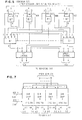
- FIGURE 1 shows a block diagram of a data processing system in which the present invention is embodied;
- FIGURE 2 shows, in a block diagram form, a cache addressing mechanism forming part of the system of Figure 1;
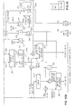
- FIGURE 3 shows how FIGURES 3A and 3B are arranged to make a complete drawing. FIGURES 3A and 3B, when arranged as shown in FIGURE 3, illustrate a cache addressing system having a synonym detection mechanism;
- FIGURE 4 shows how FIGURES 4A and 4B are arranged to make a complete drawing. FIGURES 4A and 4B show a detailed implementation of the
synonym decision logic 317 shown as a block in FIGURE 3A; - FIGURE 5 shows a detailed implementation of
encoder 327 shown in FIGURE 3B; - FIGURE 6A illustrates the machine cycle timing for a cache fetch operation having a synonym hit;
- FIGURE 6B illustrates the machine cycle timing for a cache store operation having a synonym or principle hit;
- FIGURE 7 illustrates how four chips of the type shown in FIGURE 8 may be combined to provide a cache directory which is four-way set associative and has four groups of classes;
- FIGURE 8 illustrates a single chip in the cache directory providing circuitry for one directory set with four groups of classes and compare logic;
- FIGURE 9 illustrates the machine cycle timing for a synonym fetch operation in a second embodiment shown in FIGURE 10;
- FIGURES 10, 10A and 10B show a detailed implementation for the second embodiment;
- FIGURE 11 shows the circuit details for fetch
SID circuits 371 found in the second embodiment. - Referring to FIGURE 1, a data processing system in which the present invention is embodied is shown in block diagram form. The data processing system typically comprises a main storage (MS) 10, a storage control element (SCE) 20, a buffer control element (BCE) 30 which includes a high speed buffer or
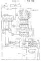
cache 311, a processor comprised of an instruction element/execution element (IE/EE) 40, an external data controller (EXDC) 50 (which may be a conventional channel processor), I/O control units anddevices 60, and a paging storage 70 (which may be a conventional bulk storage device). The IE/EE fetches or stores data in thecache 311 under the control of theBCE 30, and if the requested data is not available in thecache 311, the data is fetched from theMS 10 under the control of theSCE 20. The SCE can also transfer data betweenMS 10 and the I/O 60 or thepaging storage 70 via theEXDC 50. - Referring now to FIGURE 2, a cache addressing mechanism is explained which embodies the present invention.
- In FIGURE 2, a set-associative cache system includes a
cache 311, acache directory 309 and a directory look-aside table (DLAT) 307. Thedirectory 309 is an array which contains information about each line entry in thecache 311. TheDLAT 307 is an array which contains the most recently translated page addresses used byprocessor 40. Thecache directory 309 uses the well known concept of "set associativity" and is four-way set associative, which means that each addressable class indirectory 309 contains four entries in sets A, B, C and D. Thus, when any class in the directory is addressed, four entries A, B, C and D are accessed in parallel.Directory 309 is addressed bybits 20 through 24 of a request logical address in a buffer control address register (BCAR) 301. Bits 20-24 address one class in each of 2N groups of classes indirectory 309, so that a total of 2N classes are addressed simultaneously.-Directory 309 is constructed to simultaneously select every location which can have the translated absolute address of the requesting logical address. When 2N equals four in which N equals two virtual bits (which may comprisebits BCAR 301, four classes will be simultaneously addressed indirectory 309. The four groups of classes indirectory 309 are shown in FIGURE 2 asgroups BCAR 301 can only address the principle class indirectory 309. -
Cache 311 may contain 64K bytes divided into the four sets A,, B, C and D in which each set contains 2,048 doublewords (8 bytes). A doubleword is outputted in response to each fetch request whencache 311 is addressed by bits 18-28 fromBCAR 301 afterbits synonym control circuit 320. - The
DLAT 307 is two-way set associative with sets X and Y. A class inDLAT 307 is selected by bits 13-19 of the request inBCAR 301. Each DLAT set entry receives its content during an address translation, including: segment table origin (STO) bits from a control register (CR) 303 and bits 1-12 fromBCAR 301 representing the logical address being translated, and the translated absolute address of the page having that logical address from a dynamic address translator (DAT) 305. - Each new address request in
BCAR 301 is simultaneously used to addressdirectory 309,cache 311, andDLAT 307. Thus, BCAR address bits 13-19 select a DLAT class with entries X and Y inDLAT 307. The STO, logical address in each X and Y entry is outputted to acomparator 313 and the absolute address of the X and Y entries is outputted to acomparator 315. A comparison is then performed incomparator 313 between the STO's and logical addresses in the two selected DLAT sets X and Y with the current STO inCR 303 and the logical request address inBCAR 301. If a match occurs, it is indicated by either a LOG-X HIT signal or LOG-Y HIT signal fromcomparator 313 online 449 orline 451. - If no DLAT match occurs, the request is forced to start an address translation in
DAT 305, after which the newly translated address is placed in an appropriate set inDLAT 307, and the storage access can then be started. - Simultaneously during a DLAT access and compare in
circuit 313, the request is also causing an access incache directory 309 using BCAR bits 20-24 to select a class in each group incache directory 309. Then the directory accesses the absolute address in each of the four sets in each of the four selected directory classes and provides them to comparecircuit 315, which compares each of these 16 absolute addresses with each of the two absolute addresses received from the selected X and Y entries inDLAT 307. Thus, each request causes 32 comparisons of absolute addresses incomparator 315, which are: X:AO, X:Al, X:A2, X:A3, X:BO, X:B1, X:B2, X:B3, X:CO, X:C1, X:C2, X:C3, X:DO, X:D1, X:D2, X:D3, Y:AO, Y:Al, Y:A2, Y:A3, Y:BO, Y:B1, Y:B2, Y:B3, Y:CO, Y:Cl, Y:C2, Y:C3, Y:DO, Y:D1, Y:D2 and Y:D3. -
Decision logic 317 receives 32 compare output lines fromcomparator 315, as well asoutputs comparator 313, to determine whether a principle or synonym directory hit has occurred or not.Comparator 313 activates one of its signals LOG-X hit or LOG-Y hit if the requesting logical address was found in theDLAT 307. The outputs ofcomparators 315 indicate if either DLAT absolute address was found in any of the four classes accessed incache directory 309. If a DLAT logical address hit occurs, thencircuits 317 will determine if a cache principle hit, cache synonym hit, or a cache miss occurs. - If a cache hit has occurred,
circuits 320 output a cache group identifier (GID) which providesbits cache 311, andcircuit cache 311 is to be selected for fetching or storing a doubleword. - For a write request, a write SID is provided on a
line 347A to writeSID decoder 312, which writes the request's doubleword (DW) into the selected location incache 311. The write request's DW is written into the selected set of the selected class in the cache during the machine cycle after the directory and DLAT addressing cycle for the same request. - For a fetch request having a principle hit, the class selection in
cache 311 byCAB 310 outputs a different doubleword (DW) to each of the four cache data latches LA, LB, LC and LD for each of the four sets A, B, C, and D in the selected cache class. Each latched DW is selected from the line in each of the four sets A, B, C and D. If a hit is detected, the fetch SID is applied to setselect logic 319 to select and output the required DW in the selected cache class. The latched class of DW's in cache data latches LA, LB, LC and LD occurs at the end of the same machine cycle in which the request address is received byBCAR 301. During the next cycle, the set selected DW is outputted from setselect logic 319. - The numbers in parenthesis next to some of the lines in the drawings represent the number of actual electrical lines represented by the illustrated line.
- As the size increases for the
cache 311 and itsdirectory 309, either the number of classes or the degree of associativity must also be increased, or both, as discussed above. As mentioned previously, if the number of classes is enlarged, the cache addressing range must correspondingly be enlarged, which requiresbits BCAR 301 in FIGURE 2. - That is, the 31 bit logical address supplied to the
BCAR 301 is architecturally organized as shown at the top of FIGURE 2, in which an SX field (bits 1-11) is an index to a page table address in a segment table selected by the STO inCR 303, a PX field (bits 12-19) is an index to a page address in the selected page table; and a D field (bits 20-31) is a byte index in a 4 kilobyte page selected by the page entry. When the logical address is translated to an absolute address, bits 1-19 are changed by the translation process, but the D field bits 20-31 are not changed. Hence, the D field is sometimes called a real field in the logical address, and bits 1-19 are sometimes called a virtual field. - Each 31 bit address in
BCAR 301 is presumed to address a byte inmain storage 10. However,cache directory 309 is organized to address lines of 16 doublewords (DWs) located inmain storage 10 on line boundaries. Hence, bits 1-24 inBCAR 301 address a required line, and bit 24 is the lowest-order bit for line addressing. If only the bits in the D field were used to address the cache directory, the maximum cache address field would be 20-24, which five bits could only address a maximum of 32 classes. If more classes are required, bits from the PX field must be used,e.g. bits bit 20 for 4KB page addressing. Thus,bits - Due to the use of the two
virtual bits cache 311 may reside in any of four possible classes. The cache class pointed to by the requesting logical address is called a principle class, while the other three classes obtainable by the other three permutations of thevirtual address bits - FIGURES 3, 3A and 3B show a more detailed representation of an embodiment of the synonym detection scheme discussed in relation to FIGURE 2. In FIGURES 3A and 3B, the same reference numerals as those of FIGURE 2 are used to designate corresponding elements. Another detailed embodiment is shown in FIGURES 10, 10A, and 10B. Both embodiments in FIGURES 3 and 10 detect a synonym in the second cycle of a fetch request. The embodiment in FIGURE 3 thereafter handles the synonym fetch request in the same way as a principle hit, and takes five machine cycles for the request. The embodiment in FIGURE 10 handles a synonym fetch request without processing it like a principle hit, and takes 3 machine cycles for processing a synonym fetch request. Both embodiments in FIGURES 3 and 10 use two machine cycles to access a principle fetch or store hit, or a synonym store hit, and can pipeline these requests in one cycle.
- The following assumptions are made in both detailed embodiments: The cache (shown in FIGURE 2) is a 64KB random access memory organized to contain 512 lines in which each set contains 128 lines.
Directory 309 has four corresponding sets, and therefore is four-way set associative (sets A, B, C and D) as previously described in FIGURE 2.Directory 309 also is organized with four groups of classes as previously described. - The
DLAT 307 is two-way set associative (sets X and Y) as previously described in FIGURE 2, with 128 classes each containing an X set and a Y set.DLAT 307 is addressed with logical address bits 13-19. Each of X and Y entries contains STO bits 5-19, logical address bits 1-12 to identify a virtual page, and absolute address bits 5-19 to identify the assigned page frame inmain storage 10. - In operation, when a processor request is accepted, its associated address is loaded into the
BCAR 301, from which the address points to a class in theDLAT 307 and to a class in thecache directory 309. The DLAT class contains the STO and virtual address of two sets (X and Y), each of which is received by the comparecircuit 313 which compares them with the logical address bits 1-12 from theBCAR 301 and STO bits 5-19 from theSTO register 303. If a match occurs, the comparecircuit 313 produces either a LOG-X HIT signal or a LOG-Y HIT signal to indicate a logical address DLAT hit occurred. Simultaneously with the operation ofcircuit 313, the absolute address bits 5-19 from each set X and Y of theDLAT 307 are being provided as two compare inputs to comparecircuit 315, which is shown in FIGURE 3A as a pair of comparecircuits - There are 32 comparators in both of the compare
circuits circuits cache directory 309. Thecomparator 315X compares these sixteen absolute addresses fromdirectory 309 with the DLAT-X absolute address (ABS-X) andcomparator 315Y correspondingly compares the same cache addresses with DLAT Y absolute address (ABS-Y). If a match occurs in any comparator of 315X or 315Y, it raises a corresponding one of the 32 output lines todecision logic 317 to indicate the cache group and set having the matching absolute address. The comparators of 315X and 315Y are constructed identically and function similarly. -
Decision logic 317 receives all 32 outputs from the comparecircuits Logic 317 also receives the LOG-X HIT and LOG-Y HIT outputs from the comparecircuit 313.Logic 317 decides whether there is a synonym hit, a principle hit, or a miss. A principle hit is a hit in the principal class, which is the class pointed to by the request address bits 18-19 inBCAR 301. A principle hit is signalled when atrigger 467 is set bydecision logic 317 to output a principle hit signal online 467A. If thedecision logic 317 finds a hit in a class other than the principle class, i.e. a class pointed to by a permutation of BCAR bits 18-19, a synonym hit is said to have occurred which is signalled byline 469A from atrigger 469. Should no hit be detected,, thedecision logic 317 signals a miss online 471A. - FIGURES 4A and 4B, which are to be arranged as shown in FIGURE 4, show the internal details of
decision logic 317 found in FIGURE 3A. It comprises circuit blocks 400A, 400B, 400C and 400D for the sets A, B, C and D, respectively. Although only thecircuit block 400A is shown in detail, it should be understood that the circuit blocks 400B, 400C and 400D are identically constructed and function similarly. - The circuit structure and the operation of
circuit block 400A are explained below. Lines 429-435 and 437-443 receive the A:X and A:Y outputs, as follows: the X:AO, X:A1, X:A2, X:A3 and Y:AO, Y:Al, Y:A2, Y:A3 outputs, respectively, from the eight comparators for set A ofcircuits -
Input lines address bits BCAR 301, or (2) substitutedaddress bits BCAR bits bits gates 343 and activates a normally closed pair ofgates 341 in FIGURE 3B. - In FIGURE 4A, the
bits lines decoder 401 indecision logic 317 which activates one of four output lines that identify a particular group of classes; that is, thebit group 0, "01" decodes intogroup 1, "10" decodes intogroup 2, and "11" decodes intogroup 3. Thegroup 0 output of thedecoder 401 is applied to the other inputs of ANDgates group 1 output to ANDgates group 2 output to ANDgates group 3 output to ANDgates - During the first machine cycle for a request in
BCAR 301,lines bits - The outputs from the AND gates 403-409 are dot-ORed and applied to one input of an AND gate 419A, while the outputs from the AND gates 411-417 are dot-ORed and applied to an input of an AND gate 419B. A two-
port funnel 419 is comprised of the two AND gates 419A and 419B and an ORcircuit 419C which ORs outputs of the AND gates 419A and 419B to provide the funnel (F) output. -
Lines funnel 419. Only one of thelines funnel 419 indicates if there is a "principal class" hit in set A, because only the principle group signal is then being provided fromdecoder 401 to the gates 403-317 for set A. - There are also four other funnels F: 421, 423, 425 and 427 which are internally identical to funnel 419.
Funnels groups group 0 set A. Thus, the two comparelines 429 and 437 forgroup 0 set A fromcomparator 315 are connected to the two-port funnel 421 which also respectively receiveDLAT lines - Similarly, funnels 423, 425 and 427 receive the
group 1 set A,group 2 set A, andgroup 3 set A pairs of compare signal lines fromcomparator 315, as well as the two lines carrying the LOG-X HIT and LOG-Y HIT signals. Thus, an output from any offunnels respective group comparators - Therefore
circuit block 400A has oneoutput line 455 which exclusively signals a set A "principle hit" and has fourother output lines - Similarly, each of circuit blocks 400B, 400C and 400D receive corresponding sets of eight compare signals from
circuits bit decoder 401, and the LOG-X HIT and LOG-Y HIT signals from comparecircuit 313. Like thecircuit block 400A, each of circuit blocks 400B, 400C and 400D has one exclusive principle hit output line and four any hit lines for signalling any hit in therespective groups - The principle hit outputs from the
blocks lines circuit 453. The output from ORcircuit 453 indicates a principle class hit in any cache set A, B, C, or D. The sixteen any hit output lines (four for each set) are received by a sixteen-way ORcircuit 463, which has an output online 470 that indicates if there is any cache hit (synonym or principle hit in any of the sets A, B, C, and D). - A
decoder 465 receives the outputs of ORcircuits circuits decoder 465 in accordance with the following rules:
- Thus, the principle hit
output 467 fromdecoder 465 is activated directly by the output of ORcircuit 453. The synonym hitoutput 469 fromdecoder 465 is activated by ANDcircuit 465A if the principle hit ORcircuit 453 is not activated and the any hit ORcircuit 463 is activated. A cache miss is signalled online 471 if no any hit signal is provided from ORcircuit 463. An error condition is indicated if the principle hit ORcircuit 353 is activated while the any hit ORcircuit 363 is not activated. - An
encoder 327 receives all of the 16 any hit outputs 473-492 from thesynonym decision logic 317. - FIGURE 5 shows a detailed form of
encoder 327.Encoder 327 receives the four sets of output lines 473-479, 481-484, 485-488 and 489-492 which indicate that there was a synonym/principle hit in the respective sets A, B, C and D. If theline 473, for example, is activated, it indicates that there was a synonym or principle hit ingroup 0, set A. Similarly, if theline 482 is activated, it indicates that there was a synonym or principle hit ingroup 1, setB. Encoder 327 comprises four OR circuits which combine the respective set signals and provide them to a four-way SID encoder. Similarly, four other OR circuits combine the same signals into the four respective group signals and provide them to a four-way GID (Group Identifier) encoder. The two encoders output a hit's set identifier (SID) and group identifier (GID) in accordance with the following rules:
- In FIGURE 3, the encoded two bits for the SID are used only by a store request to select the one of four sets into which a double word will be written into the cache. The encoded two bits for the GID are provided to the
cache 311 in FIGURE 2 to select the group in which a fetch or store access is being made. - Since the cache operations to main storage resulting from a principle hit or a miss are conventional, they are not discussed further herein.
- The present embodiment is directed to a special course of action taken when a synonym hit is detected for a cache access.
- In FIGURE 3A, when a fetch request results in a synonym hit being detected by
decision logic 317, it activates the synonym hitline 469 which on the next machine cycle sets anoutput trigger 469A, and the set signal from thetrigger 469A is applied to an ANDgate 355 in FIGURE 3B, which also receives anotherinput 356 indicating the fetch request. An output from ANDgate 355 sets atrigger 329. Then the set output fromtrigger 329 through aninverter 333 toline 353 serves to close a normally open gate G2 in FIGURE 3A to inhibit the loading of a new address from theBCAR 301 to a re-do fetch address register (RFAR) 321. Normally, theRFAR 321 is loaded with the fetch address inBCAR 301 through normally open gate G2 upon the cycle following the loading ofBCAR 301. TheRFAR 321 is used as a delay register when a fetch request has a synonym hit. The set output oftrigger 329 acts as a RFAR request to aBCAR priority circuit 335, which determines which of plural possible requestors to BCAR 301 will be allowed to loadBCAR 301. An RPAR request has relatively high priority and therefore is likely to get the BCAR on the next cycle, so that the synonym fetch hit can thereafter be handled like it is a principle hit. The priorities of the requestors for BCAR have the following order: - 1. A line fetch request to update the
directory 309 and input data tocache 311. - 2. A cast out request from the cache.
- 3.
RFAR 321 request. - 4. A cross-interrogation request.
- 5. A DAT request for a table fetch while performing a translation.
- 6. An invalidate register used to hold store requests being made by I/O.
- 7. IE (processor) requests for normal fetches and stores.
- If the
BCAR priority circuit 335 gives priority to an RFAR request, it sets a RFAR accepttrigger 337. At the same time, anoutput 354 from theBCAR priority circuit 335 is applied to open a normally closed gate Gl in FIGURE 3A to transfer the content ofRFAR 321 back intoBCAR 301. At the same time an RFAR priority output fromcircuit 335 sets an RFAR accepttrigger 337, which activates a pair of ANDgates 341 and viainverter 339 deactivates ANDgates 343. Thesubstitute bits gates 341. The output from RFAR accepttrigger 337 is also applied to the reset input of thetrigger 329 to reset it to its normal state, which causesinverter circuit 339 to activate ANDgates 343 to pass the - bits 18-19 from BCAR 301 through OR circuits 345A and B to thedecision logic 317. - In FIGURE 3B, the two-bit SID and the two-bit GID from the
encoder 327 are registered in aregister 347; and the GID bits in theregister 347 are then transferred to aregister 351 through a normally open gate G3 which is opened by the reset state oftrigger 329 viainverter 333. The GID inregister 351 is then sent assubstitute bits decision logic 317 via the pair of ANDgates 341, so that thesubstitute bits decision logic 317 in place of the bits 18-19 from theBCAR 301 when a synonym hit is detected. The substitution is used during the RFAR accept trigger cycle by thedecision logic 317 when the synonym request is made to appear like a principle hit, because the substitutedbits output 467. During the cycle having the output from the RFAR accepttrigger 337 online 338, it also activates a gate G6 to transfer the GID fromregister 351 through a group select ORcircuit 359 to the cache class address bus (CAB) 310 shown in FIGURE 2. At the same time, a DWselect circuit 363 simultaneously transfers bits 20-28 received through gate G8 from theBCAR 301 to theCAB 310 to complete the cache address of the required DW. Gate G8 is activated as long as no store request is received.Cache 311 then selects the requested DW. Whenline 338 is activated, it closes a gate G7 to prevent the transfer of the BCAR bits 18-19 to register 359 by dropping the output of aninverter 381 to an ANDcircuit 382 which controls gate G7. Thus, gate G7 only operates for a principle hit to cause BCAR bits 18-19 to be gated out of groupselect circuit 359 toCAB 310. - For a store request,
select circuit 363 receives bits 20-28 from a push-down store address register (PDSAR) 361, which holds store request address bits 20-28 during the cycle after the request is received fromBCAR 301, which is when the store operation is completed. The SID bits andbits Bits gate 357 receiving the store request signal and an any hit signal online 470A. The output ofgate 357 activates a gate G4 to pass the GID fromregister 347 through the group select ORcircuit 359 toCAB 310 at thesame time circuit 363 is providing bits 20-28 fromPDSAR 361A via gate G5. - If a fetch operation detects a principle hit, BCAR bits 18-19 pass through a normally open gate G7 to group
select circuit 359, a and BCAR bits 20-28 pass through normally open gate G8 and DW select-:circuit 363. Thus, the BCAR bits 18-28 are supplied to the cache to address it with the fetch SID fromlogic 317. - A cache access by any store hit (whether principle or synonym) will write data into
cache 311 on the cycle (C2) afterBCAR 301 receives the request (on cycle 1). A cache access by a principle fetch hit supplies the requested data from the cache on the machine cycle afterBCAR 301 receives the request. A cache access by a synonym fetch hit supplies data on the fourth machine cycle afterBCAR 301 receives the request (on cycle Cl), because the synonym fetch request is temporarily stored in the RFAR so that higher priority requests can intervene and use BCAR due to the operation of theBCAR priority circuit 335. - FIGURE 6A shows a timing chart for the fetch operation when a synonym hit is detected. In a R cycle, a fetch request is brought up. The DLAT and directory comparisons are made in a Cl cycle, at the end of which a synonym hit is detected. In the following C2/DLY cycle, a fetch delayed signal is sent to the IE so that any cache data provided in this cycle is not associated with the request in the R cycle. The
RFAR 321 is loaded from BCAR and indicated to be busy. In the next DLY cycle, an RFAR request for BCAR priority is made byRFAR 321. (See BCAR PRIO 335 in FIGURE 3B.) If the RFAR request is honoured in the DLY cycle, the IE is given an advance signal. In the next Cl cycle, substitute bits 18-19 are provided byGID circuit 351 to thesynonym decision logic 317 which activates its principle hitoutput 467. Now the synonym hit looks like a principle hit and is thereafter handled in the same way as a principle hit. In the following C2 cycle, cache data is transferred to the requestor (e.g. the IE). - FIGURE 6B illustrates the timing for a store operation which always takes place on the cycle after the directory compare.
- FIGURE 7 illustrates a structure for a four-way set-associative cache directory, which uses the novel LSI chip structure shown in FIGURE 8 that includes the novel groups with comparators provided on the same chip. FIGURE 7 shows four chips A, B, C and D for the respective sets, each chip being an identical LSI chip having the novel group structure shown in FIGURE 8. Thus, BCAR real address bits 20-24 simultaneously select four directory classes respectively from the
groups decision logic 317. - The
DLAT 307 and DLAT compare 313 may also be structured from six chips of the type shown in FIGURE 8, in which three chips provide the X set and its compare logic and three other chips provide the Y set and its compare logic. - The architecture for a computer system may require that the cache directory not contain an address more than once. Also each directory address may be a main storage line address, e. g. for a line of 128 bytes. Such architecture would require that a main storage address be represented in either a principle entry or a synonym entry, but not in both at the same time. Such architecture may be enforced by having a checking circuit (not shown) check the output lines 473-479, 481-484, 485-488 and 489-492 in the embodiment to issue an error signal whenever more than one of these sixteen lines is active at any one time.
- FIGURES 10, 10A, and 10B show a second embodiment of the invention which takes less machine cycles to perform a synonym fetch than in FIGURE 3 and also results in some simplification of circuitry. That is, FIGURES 10, 10A, 10B can perform a synonym fetch in three cycles versus five cycles for FIGURES 3, 3A and 3B. The latter can use a simpler interface between the cache and processor because it makes a synonym fetch appear to the processor as a delayed principle fetch. On the other hand, FIGURES 10, 10A and 10B require a cache to processor interface which can recognize a synonym fetch cycle.
- Both embodiments in FIGURES 3 and 10 take two cycles for a synonym store operation and for a principle fetch or store operation.
- FIGURE 10A is the same as FIGURE 3A except that FIGURE 10A does not have
RFAR 321 or its gates Gl and G2. Alsobits decision logic 317 are only provided byBCAR 301; that is, there are nosubstitute bit logic 317 in FIGURE 10A. - FIGURE 10B has substantial changes from FIGURE 3B. FIGURE 10B does not have any BCAR priority control, which is provided by
circuits bit substitution circuits - Another difference is that PDAR (push down address register) 361A in FIGURE 10B receives both fetch and store request addresses from
BCAR 301, whilePDSAR 361 in FIGURE 3B receives only store request addresses. - Also only FIGURE 10B has fetch SID circuits 371 (shown in detail in FIGURE 11), which provide the SID for both principle and synonym fetches to cache
select logic 319 in FIGURE 2. Thus, in FIGURE 4A, the fetch SID output from lines 455-461 is not connected tologic 319 for the embodiment in FIGURE 10. - FIGURE 9 shows the timing for the three cycle synonym fetch hit operation of the embodiment in FIGURES 10A and 10B. The principle fetch hit and principle or synonym store hit each operate in two cycles and provide their output during the C2 cycle.
- Since only
BCAR 301 supplies addressbits funnels 419 indecision logic 317, only the principle fetch SID can be provided onoutput lines logic 317. The principle SID is delayed by one machine cycle intriggers logic 317 from which the fetch SID is provided to circuit 371 (shown in detail in FIGURE 11) during the C2 cycle in FIGURE 9. In FIGURE 11, a principle SID passes through AND gates 586-589 which are enabled and through OR circuits 591-594 to cache setselect logic 319 in FIGURE 2 during the C2 cycle. Gates 586-589 are enabled by a signal on aline 356A which is activated in FIGURE 10B by enablement of ANDgate 356 by a fetch request signal and a principle hit signal online 467A fromdecision logic 317. Hence, the DW for a principle hit is outputted fromcircuit 319 on the C2 machine cycle after the request is outputted byBCAR 301 during cycle C1. - A synonym fetch SID is outputted from
circuit 371 during the C3 cycle in FIGURE 9 when a synonym fetch signal is provided from an ANDgate 355 during the C2 cycle.Gate 355 is activated during a fetch request by a synonym hit signal online 469A fromdecision logic 317 during the C2 cycle. In FIGURE 11, the signal on line 355A is delayed during the C2 cycle by atrigger 501, which on the C3 cycle enables AND gates 581-584 to pass the decoded SID than being outputted fromtriggers lines 347A fromregister 347. The SID is then provided through OR circuits 591-594 to cacheselect logic 319. - The synonym fetch signal on line 355A also during the C2 cycle passes through an OR
circuit 358 to activate gate G4 to pass the GID fromregister 347 through group select ORcircuit 359 to providebits cache CAB 310 in FIGURE 2. - Also during the C2 cycle, the output of OR
circuit 358 causes bits 20-28 in PDAR (push down address register) 361A to be gated by G5 through DW select ORcircuit 363 to thecache CAB 310 in FIGURE 2 to complete the cache address. The PDAR always contains the value which was inBCAR 301 during the prior Cl machine cycle.Inverter 383 during the C2 cycle inhibits both gates G7 and G8 to prevent any bits currently inBCAR 301 from then being received by select ORcircuits - In summary, the SID and GID signals .are held during the C2 machine cycle in
register 347. Also the SID is held for the C3 cycle incircuits 371 when they provide the SID to the setselect logic 319. The doubleword accessed from the cache is then provided to the requestor, e.g. IE/EE, from the output oflogic 319 during the C3 cycle. - Any store request hit activates AND
gate 357 which also activates the output of ORcircuit 358 to enable gates G4 and G5 to pass the GID fromregister 347 and the PDAR bits 20-28 fromcircuit 359 toC AB 310 during a C2 cycle. Also during the C2 cycle, the SID fromregister 347 is passed to thewrite SID decoder 312 in FIGURE 2 to write the doubleword of data provided by the requestor into the proper set incache 311 to complete the store request. - While the present invention has been shown and described with reference to preferred embodiments which use a four-way set associative cache, with four groups of classes, it should be understood that any 2N number of groups may be used and any degree of set associativity may be used including no set associativity.
Claims (20)
Applications Claiming Priority (2)
| Application Number | Priority Date | Filing Date | Title |
|---|---|---|---|
| US06/130,946 US4332010A (en) | 1980-03-17 | 1980-03-17 | Cache synonym detection and handling mechanism |
| US130946 | 1980-03-17 |
Publications (3)
| Publication Number | Publication Date |
|---|---|
| EP0036110A2 true EP0036110A2 (en) | 1981-09-23 |
| EP0036110A3 EP0036110A3 (en) | 1983-10-05 |
| EP0036110B1 EP0036110B1 (en) | 1987-06-16 |
Family
ID=22447126
Family Applications (1)
| Application Number | Title | Priority Date | Filing Date |
|---|---|---|---|
| EP81101360A Expired EP0036110B1 (en) | 1980-03-17 | 1981-02-25 | Cache addressing mechanism |
Country Status (4)
| Country | Link |
|---|---|
| US (1) | US4332010A (en) |
| EP (1) | EP0036110B1 (en) |
| JP (1) | JPS604494B2 (en) |
| DE (1) | DE3176266D1 (en) |
Cited By (4)
| Publication number | Priority date | Publication date | Assignee | Title |
|---|---|---|---|---|
| EP0140528A2 (en) * | 1983-08-31 | 1985-05-08 | Amdahl Corporation | Apparatus for reverse translation |
| EP0206050A2 (en) * | 1985-06-28 | 1986-12-30 | Hewlett-Packard Company | Virtually addressed cache memory with physical tags |
| EP0212678A2 (en) | 1980-11-10 | 1987-03-04 | International Business Machines Corporation | Cache storage synonym detection and handling means |
| EP0224168A2 (en) * | 1985-11-19 | 1987-06-03 | Hitachi, Ltd. | Buffer storage control system |
Families Citing this family (64)
| Publication number | Priority date | Publication date | Assignee | Title |
|---|---|---|---|---|
| JPS6028015B2 (en) * | 1980-08-28 | 1985-07-02 | 日本電気株式会社 | information processing equipment |
| US4399506A (en) * | 1980-10-06 | 1983-08-16 | International Business Machines Corporation | Store-in-cache processor means for clearing main storage |
| US4400770A (en) * | 1980-11-10 | 1983-08-23 | International Business Machines Corporation | Cache synonym detection and handling means |
| US4523275A (en) * | 1980-11-14 | 1985-06-11 | Sperry Corporation | Cache/disk subsystem with floating entry |
| US4481573A (en) * | 1980-11-17 | 1984-11-06 | Hitachi, Ltd. | Shared virtual address translation unit for a multiprocessor system |
| US4661903A (en) * | 1981-05-22 | 1987-04-28 | Data General Corporation | Digital data processing system incorporating apparatus for resolving names |
| US4464712A (en) * | 1981-07-06 | 1984-08-07 | International Business Machines Corporation | Second level cache replacement method and apparatus |
| JPS58147879A (en) * | 1982-02-26 | 1983-09-02 | Toshiba Corp | Control system of cache memory |
| JPS58150186A (en) * | 1982-03-03 | 1983-09-06 | Nec Corp | System for controlling buffer memory |
| US4511994A (en) * | 1982-09-27 | 1985-04-16 | Control Data Corporation | Multi-group LRU resolver |
| US4594659A (en) * | 1982-10-13 | 1986-06-10 | Honeywell Information Systems Inc. | Method and apparatus for prefetching instructions for a central execution pipeline unit |
| US4607331A (en) * | 1983-05-13 | 1986-08-19 | Motorola, Inc. | Method and apparatus for implementing an algorithm associated with stored information |
| US4731739A (en) * | 1983-08-29 | 1988-03-15 | Amdahl Corporation | Eviction control apparatus |
| US4589092A (en) * | 1983-12-12 | 1986-05-13 | International Business Machines Corporation | Data buffer having separate lock bit storage array |
| US4807110A (en) * | 1984-04-06 | 1989-02-21 | International Business Machines Corporation | Prefetching system for a cache having a second directory for sequentially accessed blocks |
| JPH0670787B2 (en) * | 1984-06-29 | 1994-09-07 | 富士通株式会社 | Command transfer control system between processors |
| US4747044A (en) * | 1984-08-23 | 1988-05-24 | Ncr Corporation | Direct execution of software on microprogrammable hardware |
| US4648033A (en) * | 1984-09-07 | 1987-03-03 | International Business Machines Corporation | Look-aside buffer LRU marker controller |
| JPS6184753A (en) * | 1984-10-01 | 1986-04-30 | Hitachi Ltd | Associative buffer memory |
| US4663742A (en) * | 1984-10-30 | 1987-05-05 | International Business Machines Corporation | Directory memory system having simultaneous write, compare and bypass capabilites |
| JP2539357B2 (en) * | 1985-03-15 | 1996-10-02 | 株式会社日立製作所 | Data processing device |
| US4636990A (en) * | 1985-05-31 | 1987-01-13 | International Business Machines Corporation | Three state select circuit for use in a data processing system or the like |
| US5029072A (en) * | 1985-12-23 | 1991-07-02 | Motorola, Inc. | Lock warning mechanism for a cache |
| US4755936A (en) * | 1986-01-29 | 1988-07-05 | Digital Equipment Corporation | Apparatus and method for providing a cache memory unit with a write operation utilizing two system clock cycles |
| US5237671A (en) * | 1986-05-02 | 1993-08-17 | Silicon Graphics, Inc. | Translation lookaside buffer shutdown scheme |
| JPH0661066B2 (en) * | 1986-10-20 | 1994-08-10 | 株式会社日立製作所 | Storage controller |
| US4797817A (en) * | 1986-12-10 | 1989-01-10 | Ncr Corporation | Single cycle store operations in a virtual memory |
| US5119290A (en) * | 1987-10-02 | 1992-06-02 | Sun Microsystems, Inc. | Alias address support |
| KR920001282B1 (en) * | 1987-10-02 | 1992-02-10 | 가부시키가이샤 히타치세이사쿠쇼 | Buffer memory control apparatus |
| JPH07120312B2 (en) * | 1987-10-07 | 1995-12-20 | 株式会社日立製作所 | Buffer memory controller |
| US5133061A (en) * | 1987-10-29 | 1992-07-21 | International Business Machines Corporation | Mechanism for improving the randomization of cache accesses utilizing abit-matrix multiplication permutation of cache addresses |
| US4897813A (en) * | 1988-02-19 | 1990-01-30 | Unisys Corporation | Partially programmable read-only memory system |
| US5003459A (en) * | 1988-04-01 | 1991-03-26 | Digital Equipment Corporation | Cache memory system |
| US5214770A (en) * | 1988-04-01 | 1993-05-25 | Digital Equipment Corporation | System for flushing instruction-cache only when instruction-cache address and data-cache address are matched and the execution of a return-from-exception-or-interrupt command |
| DE68926837T2 (en) * | 1988-06-07 | 1997-03-06 | Bull Hn Information Syst | Device and method for improved conversion from virtual to real address for cache memory access |
| US5226146A (en) * | 1988-10-28 | 1993-07-06 | Hewlett-Packard Company | Duplicate tag store purge queue |
| US5142634A (en) * | 1989-02-03 | 1992-08-25 | Digital Equipment Corporation | Branch prediction |
| GB9008145D0 (en) * | 1989-05-31 | 1990-06-06 | Ibm | Microcomputer system employing address offset mechanism to increase the supported cache memory capacity |
| US5148538A (en) * | 1989-10-20 | 1992-09-15 | International Business Machines Corporation | Translation look ahead based cache access |
| US5265227A (en) * | 1989-11-14 | 1993-11-23 | Intel Corporation | Parallel protection checking in an address translation look-aside buffer |
| JP2503702B2 (en) * | 1989-12-19 | 1996-06-05 | 日本電気株式会社 | Address translation device |
| US5206941A (en) * | 1990-01-22 | 1993-04-27 | International Business Machines Corporation | Fast store-through cache memory |
| JPH03216744A (en) * | 1990-01-22 | 1991-09-24 | Fujitsu Ltd | Built-in cache memory control system |
| US5014195A (en) * | 1990-05-10 | 1991-05-07 | Digital Equipment Corporation, Inc. | Configurable set associative cache with decoded data element enable lines |
| US5283876A (en) * | 1990-10-05 | 1994-02-01 | Bull Hn Information Systems Inc. | Virtual memory unit utilizing set associative memory structure and state machine control sequencing with selective retry |
| JP2734466B2 (en) * | 1991-05-02 | 1998-03-30 | 三菱電機株式会社 | Microcomputer |
| JP2839060B2 (en) * | 1992-03-02 | 1998-12-16 | インターナショナル・ビジネス・マシーンズ・コーポレイション | Data processing system and data processing method |
| US5584002A (en) * | 1993-02-22 | 1996-12-10 | International Business Machines Corporation | Cache remapping using synonym classes |
| US5813046A (en) * | 1993-11-09 | 1998-09-22 | GMD--Forschungszentrum Informationstechnik GmbH | Virtually indexable cache memory supporting synonyms |
| DE19512745A1 (en) * | 1994-04-15 | 1995-10-26 | Mathematik Und Datenverarbeitu | Cache memory device for storing data |
| JPH07287668A (en) * | 1994-04-19 | 1995-10-31 | Hitachi Ltd | Data processor |
| US5890221A (en) * | 1994-10-05 | 1999-03-30 | International Business Machines Corporation | Method and system for offset miss sequence handling in a data cache array having multiple content addressable field per cache line utilizing an MRU bit |
| US6006312A (en) * | 1995-02-27 | 1999-12-21 | Sun Microsystems, Inc. | Cachability attributes of virtual addresses for optimizing performance of virtually and physically indexed caches in maintaining multiply aliased physical addresses |
| US5649155A (en) * | 1995-03-31 | 1997-07-15 | International Business Machines Corporation | Cache memory accessed by continuation requests |
| US5894487A (en) * | 1997-07-15 | 1999-04-13 | International Business Machines Corporation | Error detection of directory arrays in dynamic circuits |
| CN1168025C (en) * | 1999-03-10 | 2004-09-22 | 国际商业机器公司 | Command cache for multiple thread processor |
| US7283991B1 (en) * | 1999-03-11 | 2007-10-16 | Microsoft Corporation | Caching system for path search optimization |
| US6629207B1 (en) | 1999-10-01 | 2003-09-30 | Hitachi, Ltd. | Method for loading instructions or data into a locked way of a cache memory |
| US6772325B1 (en) * | 1999-10-01 | 2004-08-03 | Hitachi, Ltd. | Processor architecture and operation for exploiting improved branch control instruction |
| US6553460B1 (en) | 1999-10-01 | 2003-04-22 | Hitachi, Ltd. | Microprocessor having improved memory management unit and cache memory |
| US6412043B1 (en) | 1999-10-01 | 2002-06-25 | Hitachi, Ltd. | Microprocessor having improved memory management unit and cache memory |
| US6598128B1 (en) | 1999-10-01 | 2003-07-22 | Hitachi, Ltd. | Microprocessor having improved memory management unit and cache memory |
| US6658505B2 (en) * | 2001-06-05 | 2003-12-02 | Hewlett-Packard Development Company, L.P. | System and method for checking bits in a buffer with multiple entries |
| US9430395B2 (en) * | 2008-08-11 | 2016-08-30 | International Business Machines Corporation | Grouping and dispatching scans in cache |
Citations (4)
| Publication number | Priority date | Publication date | Assignee | Title |
|---|---|---|---|---|
| FR2144265A5 (en) * | 1971-06-30 | 1973-02-09 | Ibm | |
| US3723976A (en) * | 1972-01-20 | 1973-03-27 | Ibm | Memory system with logical and real addressing |
| US4096573A (en) * | 1977-04-25 | 1978-06-20 | International Business Machines Corporation | DLAT Synonym control means for common portions of all address spaces |
| US4136385A (en) * | 1977-03-24 | 1979-01-23 | International Business Machines Corporation | Synonym control means for multiple virtual storage systems |
Family Cites Families (5)
| Publication number | Priority date | Publication date | Assignee | Title |
|---|---|---|---|---|
| US3902164A (en) * | 1972-07-21 | 1975-08-26 | Ibm | Method and means for reducing the amount of address translation in a virtual memory data processing system |
| JPS52149444A (en) * | 1976-06-08 | 1977-12-12 | Fujitsu Ltd | Multiplex virtual space processing data processing system |
| US4084230A (en) * | 1976-11-29 | 1978-04-11 | International Business Machines Corporation | Hybrid semiconductor memory with on-chip associative page addressing, page replacement and control |
| US4218743A (en) * | 1978-07-17 | 1980-08-19 | International Business Machines Corporation | Address translation apparatus |
| US4264953A (en) * | 1979-03-30 | 1981-04-28 | Honeywell Inc. | Virtual cache |
-
1980
- 1980-03-17 US US06/130,946 patent/US4332010A/en not_active Expired - Lifetime
-
1981
- 1981-02-25 EP EP81101360A patent/EP0036110B1/en not_active Expired
- 1981-02-25 DE DE8181101360T patent/DE3176266D1/en not_active Expired
- 1981-03-10 JP JP56033287A patent/JPS604494B2/en not_active Expired
Patent Citations (4)
| Publication number | Priority date | Publication date | Assignee | Title |
|---|---|---|---|---|
| FR2144265A5 (en) * | 1971-06-30 | 1973-02-09 | Ibm | |
| US3723976A (en) * | 1972-01-20 | 1973-03-27 | Ibm | Memory system with logical and real addressing |
| US4136385A (en) * | 1977-03-24 | 1979-01-23 | International Business Machines Corporation | Synonym control means for multiple virtual storage systems |
| US4096573A (en) * | 1977-04-25 | 1978-06-20 | International Business Machines Corporation | DLAT Synonym control means for common portions of all address spaces |
Non-Patent Citations (1)
| Title |
|---|
| IBM TECHNICAL DISCLOSURE BULLETIN, vol. 22, no. 8A, January 1980, pages 3331-3333, New York, USA J.M. LEE et al.: "A solution to the synonym problem" * |
Cited By (8)
| Publication number | Priority date | Publication date | Assignee | Title |
|---|---|---|---|---|
| EP0212678A2 (en) | 1980-11-10 | 1987-03-04 | International Business Machines Corporation | Cache storage synonym detection and handling means |
| EP0212678A3 (en) * | 1980-11-10 | 1987-08-12 | International Business Machines Corporation | Cache storage synonym detection and handling means |
| EP0140528A2 (en) * | 1983-08-31 | 1985-05-08 | Amdahl Corporation | Apparatus for reverse translation |
| EP0140528A3 (en) * | 1983-08-31 | 1987-09-30 | Amdahl Corporation | Apparatus for reverse translation |
| EP0206050A2 (en) * | 1985-06-28 | 1986-12-30 | Hewlett-Packard Company | Virtually addressed cache memory with physical tags |
| EP0206050A3 (en) * | 1985-06-28 | 1990-03-14 | Hewlett-Packard Company | Virtually addressed cache memory with physical tags |
| EP0224168A2 (en) * | 1985-11-19 | 1987-06-03 | Hitachi, Ltd. | Buffer storage control system |
| EP0224168A3 (en) * | 1985-11-19 | 1990-03-14 | Hitachi, Ltd. | Buffer storage control system |
Also Published As
| Publication number | Publication date |
|---|---|
| JPS56140575A (en) | 1981-11-02 |
| US4332010A (en) | 1982-05-25 |
| DE3176266D1 (en) | 1987-07-23 |
| EP0036110B1 (en) | 1987-06-16 |
| JPS604494B2 (en) | 1985-02-04 |
| EP0036110A3 (en) | 1983-10-05 |
Similar Documents
| Publication | Publication Date | Title |
|---|---|---|
| US4332010A (en) | Cache synonym detection and handling mechanism | |
| KR920005280B1 (en) | High speed cache system | |
| KR100369923B1 (en) | Data processing device | |
| US5526504A (en) | Variable page size translation lookaside buffer | |
| JP2618175B2 (en) | History table of virtual address translation prediction for cache access | |
| US4797814A (en) | Variable address mode cache | |
| US6920531B2 (en) | Method and apparatus for updating and invalidating store data | |
| US5265227A (en) | Parallel protection checking in an address translation look-aside buffer | |
| US4731739A (en) | Eviction control apparatus | |
| US4612612A (en) | Virtually addressed cache | |
| US6532528B1 (en) | Data processor and data processor system having multiple modes of address indexing and operation | |
| EP0373780B1 (en) | Address translation for multiple-sized pages | |
| US6014732A (en) | Cache memory with reduced access time | |
| US4682281A (en) | Data storage unit employing translation lookaside buffer pointer | |
| US5630097A (en) | Enhanced cache operation with remapping of pages for optimizing data relocation from addresses causing cache misses | |
| JP4065660B2 (en) | Translation index buffer with distributed functions in parallel | |
| US6493812B1 (en) | Apparatus and method for virtual address aliasing and multiple page size support in a computer system having a prevalidated cache | |
| US6304944B1 (en) | Mechanism for storing system level attributes in a translation lookaside buffer | |
| US6473835B2 (en) | Partition of on-chip memory buffer for cache | |
| JP2010518519A (en) | Address translation method and apparatus | |
| JPH07295886A (en) | Computer system with hierarchical memory and hierachical memory and hierarchical memory management method | |
| US5539892A (en) | Address translation lookaside buffer replacement apparatus and method with user override | |
| KR920001282B1 (en) | Buffer memory control apparatus | |
| US6510506B2 (en) | Error detection in cache tag array using valid vector | |
| US6574698B1 (en) | Method and system for accessing a cache memory within a data processing system |
Legal Events
| Date | Code | Title | Description |
|---|---|---|---|
| PUAI | Public reference made under article 153(3) epc to a published international application that has entered the european phase |
Free format text: ORIGINAL CODE: 0009012 |
|
| AK | Designated contracting states |
Designated state(s): DE FR GB IT |
|
| 17P | Request for examination filed |
Effective date: 19821220 |
|
| PUAL | Search report despatched |
Free format text: ORIGINAL CODE: 0009013 |
|
| AK | Designated contracting states |
Designated state(s): DE FR GB IT |
|
| GRAA | (expected) grant |
Free format text: ORIGINAL CODE: 0009210 |
|
| AK | Designated contracting states |
Kind code of ref document: B1 Designated state(s): DE FR GB IT |
|
| PG25 | Lapsed in a contracting state [announced via postgrant information from national office to epo] |
Ref country code: IT Free format text: LAPSE BECAUSE OF FAILURE TO SUBMIT A TRANSLATION OF THE DESCRIPTION OR TO PAY THE FEE WITHIN THE PRESCRIBED TIME-LIMIT;WARNING: LAPSES OF ITALIAN PATENTS WITH EFFECTIVE DATE BEFORE 2007 MAY HAVE OCCURRED AT ANY TIME BEFORE 2007. THE CORRECT EFFECTIVE DATE MAY BE DIFFERENT FROM THE ONE RECORDED. Effective date: 19870616 |
|
| REF | Corresponds to: |
Ref document number: 3176266 Country of ref document: DE Date of ref document: 19870723 |
|
| ET | Fr: translation filed | ||
| PLBE | No opposition filed within time limit |
Free format text: ORIGINAL CODE: 0009261 |
|
| STAA | Information on the status of an ep patent application or granted ep patent |
Free format text: STATUS: NO OPPOSITION FILED WITHIN TIME LIMIT |
|
| 26N | No opposition filed | ||
| PGFP | Annual fee paid to national office [announced via postgrant information from national office to epo] |
Ref country code: GB Payment date: 19910118 Year of fee payment: 11 |
|
| PGFP | Annual fee paid to national office [announced via postgrant information from national office to epo] |
Ref country code: FR Payment date: 19910123 Year of fee payment: 11 |
|
| PGFP | Annual fee paid to national office [announced via postgrant information from national office to epo] |
Ref country code: DE Payment date: 19910204 Year of fee payment: 11 |
|
| PG25 | Lapsed in a contracting state [announced via postgrant information from national office to epo] |
Ref country code: GB Effective date: 19920225 |
|
| GBPC | Gb: european patent ceased through non-payment of renewal fee | ||
| PG25 | Lapsed in a contracting state [announced via postgrant information from national office to epo] |
Ref country code: FR Effective date: 19921030 |
|
| PG25 | Lapsed in a contracting state [announced via postgrant information from national office to epo] |
Ref country code: DE Effective date: 19921103 |
|
| REG | Reference to a national code |
Ref country code: FR Ref legal event code: ST |