EP0051794A1 - Distributed-structure message switching system on random-access channel for message dialogue among processing units - Google Patents
Distributed-structure message switching system on random-access channel for message dialogue among processing units Download PDFInfo
- Publication number
- EP0051794A1 EP0051794A1 EP81109021A EP81109021A EP0051794A1 EP 0051794 A1 EP0051794 A1 EP 0051794A1 EP 81109021 A EP81109021 A EP 81109021A EP 81109021 A EP81109021 A EP 81109021A EP 0051794 A1 EP0051794 A1 EP 0051794A1
- Authority
- EP
- European Patent Office
- Prior art keywords
- channel
- message
- apt
- bit
- address
- Prior art date
- Legal status (The legal status is an assumption and is not a legal conclusion. Google has not performed a legal analysis and makes no representation as to the accuracy of the status listed.)
- Granted
Links
- 238000012545 processing Methods 0.000 title claims abstract description 33
- 230000005540 biological transmission Effects 0.000 claims abstract description 35
- 230000000295 complement effect Effects 0.000 claims description 3
- 230000000694 effects Effects 0.000 claims 2
- 238000000034 method Methods 0.000 description 11
- 238000012546 transfer Methods 0.000 description 6
- 239000000284 extract Substances 0.000 description 5
- 239000013256 coordination polymer Substances 0.000 description 3
- 238000010586 diagram Methods 0.000 description 3
- 238000004891 communication Methods 0.000 description 2
- 230000001360 synchronised effect Effects 0.000 description 2
- 238000012360 testing method Methods 0.000 description 2
- 230000002457 bidirectional effect Effects 0.000 description 1
- 230000001934 delay Effects 0.000 description 1
- 230000001627 detrimental effect Effects 0.000 description 1
- 238000005516 engineering process Methods 0.000 description 1
- 230000000977 initiatory effect Effects 0.000 description 1
- 239000013307 optical fiber Substances 0.000 description 1
- 230000011664 signaling Effects 0.000 description 1
Images

Classifications
-
- G—PHYSICS
- G06—COMPUTING; CALCULATING OR COUNTING
- G06F—ELECTRIC DIGITAL DATA PROCESSING
- G06F13/00—Interconnection of, or transfer of information or other signals between, memories, input/output devices or central processing units
- G06F13/14—Handling requests for interconnection or transfer
- G06F13/36—Handling requests for interconnection or transfer for access to common bus or bus system
- G06F13/368—Handling requests for interconnection or transfer for access to common bus or bus system with decentralised access control
- G06F13/374—Handling requests for interconnection or transfer for access to common bus or bus system with decentralised access control using a self-select method with individual priority code comparator
Definitions
- the present invention relates to message-switching communications systems and in particular it concerns a distributed-structure connection network on random-access channel for message dialogue among processing units.
- ALOHA Abramson - F. Kuo. "The Aloha system”. Computer Communication Network - Prentice-Hall Inc. 1973) wherein different stations broadcast their messages towards a centralized one.
- ALOHA system and of many other similar systems consist in a low efficiency attainable on the transmission media and in a possible instability and saturation of the channel owing to the occurrence of multiple collisions which cause repeated message retransmissions: Under particular conditions the channel saturation can take place even for long time periods, during which the "throughput" is reduced to zero.
- the system provided by the present invention, has a structure entirely-distributed among the various interconnected processing units, with the only exception of the time base, which distributes the synchronism signal, and of the same connection bus; the result brings to a high reliability system.
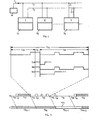
- Reference BT in Fig. 1 denotes a usual time base apt to generate over a service line 1 the synchronism signal necessary to the alignment of the units constituting the system.
- Reference Ul, U2, ... Ui denote a number of local processing units, distributed over not too wide an area, arranged to receive and send messages via a bidirectional data line (channel) denoted by 2, depending on the timing signal they receive from BT via line 1.
- processing units U can be of any known type.
- each processing unit U originates a data traffic of the "burst" type, consisting of asynchronous messages independent of the ones emitted by the other units.
- the lines 1 and 2 are a support for the data transfer and can physically consist of different types of transmission means, such as: coaxial cable, "twisted pair", optical fibre, etc.
- reference DR1 denotes a driver, of known type, of line 1 with an open-collector output allowing a determined logic level (for instance "0") to prevail over the service line.
- Reference DR2 denotes a driver of channel 2, apt to be connected on the same channel to other drivers of the same type, allocated in the remaining processing units.
- References RSI and RS2 denote two circuits of known type apt to the reception of the bit stream present on lines 1 or 2 respectively.
- References LR and LT denote two logic circuits, basically consisting of usual shift registers, arranged to_transfer the data stream from and to channel 2 respectively through RS2 e DR2.
- Reference BRX denotes a usual buffer, consisting for instance of a FIFO memory (first in, first out) apt to the temporary storage of data coming from channel 2 through RS2 and LR, addressed to the processing unit Ui.
- FIFO memory first in, first out
- Reference BTX denotes a usual buffer, it too consisting for instance of a FIFO memory, apt to the temporary storage of data coming from units Ui to be forwarded towards the channel 2, through LT and DR2.
- Reference RSC denotes a parallel register storing the commands the processing unit Ui transmits to I.
- Reference RI denotes a parallel register, containing an identification address of the unit U, which either has been previously fixed by unit Ui itself or can simply be wired once for all. In the latter case connection 9 between Ui and RI is useless.
- Reference CP denotes a known circuit apt to compare the address contained in RI with that contained, as will be seen, in a determined information field of the messages received by channel 2.
- Reference LS denotes a circuit which extracts from the ; data stream received from RS2 via channel 2, the transmission frequency of said data.
- the main component of circuit LS is a normal PLL (phase locked loop.).
- LRI denotes a logie, basically consisting of a usual shift register, apt to transmit the address stored in RI over the line 1 by means of LII, which will be examined hereinafter, and of DR1, upon the command it receives from RSC.
- Reference LII denotes a circuit of known kind apt to complement to 1 the address bits, it receives from LRI, when it receives a definite command from RSC. LII forwards the bits on the service line through DRI.
- Reference LEC denotes a usual comparison circuit for comparing the address bits, present at the LII output and those received from service line 1, through RSI.
- Reference LLI denotes a logic circuit arranged to:
- Reference BTI denotes a time base of any known type, apt to generate the bit transmission frequency on the line service.
- BTI receives, through RS1 the synchronism signal, present on service line 1, and gets synchronized with it.
- Reference CTS denotes a usual down counter apt to store the number which expresses the duration of a message as multiples of time-slots TS. CTS is decremented by a unit at each time slot elapsed during the message transmission.
- CTS is connected at the input to Ui, through connection 21, and at the output to LLI through wires 22 and 23.
- Fig. 3 a time diagram is depicted which puts in relationship the synchronism signal emitted by BT on line 1 with the address signals emitted on the same line 1 by three hypothetical processing units Ux,Uy, Uz.
- the time interval comprised between two subsequent synchronism signals defines time slot TS.
- Time slot TS is subdivided into three parts: the first part t so is intended for the synchronism signal, which for instance may consist of the bit sequence 00001 represented in the drawing; the second part t S1 is allotted to a bit L/I which when at logic level "1", indicates that the data channel (line 2) is available; the last part t S2 is intended for the address bits of each unit U.
- each unit U is univocally identified by its own address; however, it is clear that no configuration capable of simulating the synchronism signal ought to be allotted.
- Each time slot TS of service line 1 corresponds on line 2 to an equal time period the single units U can dispose of for the transmission of their own data.
- the method, according to which the various units U are enabled to transmit on the channel (line 2) will be seen hereinbelow.
- channel time TS h has been extended, indicating by IU k , IU y , IUz the addresses of units Ux, Uy, Uz; in addition the busy state of channel 2 has been emphasized, denoting by MUy the message actually transmitted by unit Uy.
- Fig. 3 shows the collision methodology, the channel acquisition and the subsequent message transmission.
- Unit Uy is the winner since, as will be seen hereinbelow its address has a greater priority than the address of the other two units and so it secures its access to the channel in the subsequent time slot.
- unit Uy transmits its message MUy which, since in the cited example MUy is a message of length comprised between one and two time-slots, resets bit L/I, contained in portion t S1 of TS n+1 .
- bit L/I is restored at time slot TS n+2 to allow possible successive channel acquisition conflicts.
- Time base BT (Fig. 1) emits on the line 1 towards all the units U a synchronism signal in time t S0 of each time slot TS (Fig. 3).
- the units which have a message to transmit, upon reception of said synchronism signal and provided the channel is available (bit L/I of t S1 at "1") emit, through their interface I, on the same line 1 their address.
- line I is implemented according to the digital technique with one logic level prevailing over the other (for instance with prevailing logic level "0"), if at the same bit time two or more units U happen to emit over line 1 different logic levels, level "0" is always prevailing.
- each unit U effecting a control between the emitted bit and the bit received by line 1, in case of discrepancy between the two levels, notices that at least oneother unit exists which simultaneously transmits on line 1 with higher priority.
- the unit or the units, which have detected such a discrepancy interrupt their transmission.
- the comparison is executed for all the address bits; at the end of the last bit, an only unit will be sure it has correctly transmitted its address on line 1 and therefore it has secured the channel acquisition. Therefore at the subsequent TS, the unit can begin the transmission of its own data.
- a unit U If a unit U is to transmit a message requiring more than one time slot for its transmission, the unit can-maintain the channel possession by resetting to "0" the bit of field t S1 of TS (Fig. 3) for all the successive time slots necessary to the message transmission.
- the format of the data message which are transmitted on the channel can be organized in whatever suitable way, provided indications are given relating to the sender and addressee identities and, in the systems in which there is no resorting to fixed-length messages the indication of the length itself.
- the message format therefore becomes similar to that of high-level protocol, of the SDLC/HDLC kind, known to the person skilled in the art.
- Ui sends the message, organized as already seen, through connection 3 into transmission buffer BTX and at the same time, through a command sent to register RSC through connection 4, it starts the process to gain the access to the already examined channel.
- RSC transfers, through connection 5, said command to blocks LLI and LRI.
- LLI upon this command and the signal it receives from BTI through wire 6, indicating the bit time t si , samples the logic state of line 1, it receives through RS1 and wire 7, in order to know whether at the time of the subsequent time slot the channel is available or it has already been engaged.
- LLI finds out the channel busy-state (bit L/I at logic value "0") it begins repeating the same test at the subsequent time--slot or time-slots till the channel is found disengaged.
- LLI finds out the free state (bit L/I at "1") it sends the command to LRI, through connection 8, of transmitting on line 1, through wire 11, LII, the wire 12 and DR1, the first bit of the address of unit Ui it extracts from RI through connection 10.
- the transmission time of said bit and of all the subsequent ones, as will be seen hereinafter, is supplied to LRI from time base BTI on wire 32.
- the transmitted address bit is also sent, through wire 12, prior to being transferred on line 1 through DR1, to comparison circuit LEG.
- LEG makes the comparison between the values of the two received bits, upon the synchronization it receives from BTI on wire 13, taking into account the propagation delays on the service line.
- LEG sends to LRI, through connection 14, a signal allowing LRI to begin the transmission of the second address bit; if, on the contrary, the two bits are different, LEG sends to LRI, still through connection 14, a stop command for the transmission in progress.
- the stop lasts for the whole time of the time slot and of possible subsequent ones, in case logic LLI finds out, depending on the examination of bit L/I, the channel busy state.
- logic LRI signals through connection 15 to LT that at the subsequent time slot it can begin the transmission on the data message channel.
- LT extracts the message from BTX through connection 17 and sends it serially through wire 16 and DR2 after enabling, upon command on wire 33, the latter to transmit.
- the data message bit overflow from BTX to LT occurs in parallel on connection 17, depending on the usual data transfer commands exchanged by BTX and LT through connection 18.
- Data message transmission on the channel is synchronously effected by LT at the beginning of time slot TS, depending on the signal LT receives from BTI via wire 19, at a frequency supplied by LS, through wire 20.
- LLI depending on the signal it receives from CTS on wire 22, sends to LRI on connection 8 the command of resetting to "0" the bit L/I of t S1 (Fig. 3) for all the necessary time slots.
- the information on the number of time slots necessary to a given message is supplied to the counter CTS from Ui by means of connection 21.
- CTS is decremented by a unit at each time slot of effective message transmission from LLI via wire 23.
- CTS at the end of the counting, results to be reset and takes off the reset command of bit L/I for LLI; therefore bit L/I is returned to logic value "1" indicating that, starting from the subsequent time slot ) the channel is available.
- the transmission logic LT communicates it to unit Ui through wire 24.
- action may be taken to complement the address field as a consequence of each transmission by a command which Ui sends to LII through wire 4, RSC and wire 31.
- the interface of Fig. 2 is also capable of receiving the messages which transit on line 2, generated by other units U different from Ui or even those generated by Ui itself.
- the latter case can advantageously be used to perform a number of tests of operation of the interface itself.
- LR extracts the.content of the address area of the received message and sends it to comparator CP.
- CP makes the comparison between the address it receives from LR and the address received from RI through connection 10, or with the pre-wired address and sends this result to LR via wire 28.
- LR transfers the message contents, in parallel, through connection 26 to buffer BRX.
- BTX and LR exchange commands and information on the message transfer through connection 27.
Abstract
Description
- The present invention relates to message-switching communications systems and in particular it concerns a distributed-structure connection network on random-access channel for message dialogue among processing units.
- Whenever a given number of independent processing units are to mutually exchange information, the problem arises of optimizing the dialogue among them.
- Various systems are known in the technique which allow a more or less optimal message-exchange. The main systems are:
- - systems providing fully-meshed point-to-point connection of all the involved processing units. This kind of system obviously requires a high number of connections, the higher the processing-units number, the more complex the system;
- - time-division synchronous systems, according to which the connection line among the units is subdivided into time slots, which usually are as many, as are the connected units. This system is efficient when the traffic which originates in the various units has regularity and continuity characteristics, but it becomes inefficient when the nature of the traffic ns of"burst" type (i. e. highpeaks on low mean value) like the traffic generally originated by the processing units which constitute the nodes of the message switching systems;
- - systems resorting to a single connection bus equipped with a control and arbitration unit, apt to resolve the conflicts of access (contention) to the bus by the various processing units. These systems are complex and expensive; furthermore they are not highly reliable as a failure of the arbitration logic can be detrimental to the whole-system operation;
- - systems, which have random access to a common transmission source. The messages are transmitted without taking into account the collision with messages from other stations; suitable methodologies have to be envisaged to recognize collisions among the messages and to determine their retransmission criteria.
- One of the first examples of embodiment of this kind is found in ALOHA (N. Abramson - F. Kuo. "The Aloha system". Computer Communication Network - Prentice-Hall Inc. 1973) wherein different stations broadcast their messages towards a centralized one.
- The main disadvantages of ALOHA system, and of many other similar systems consist in a low efficiency attainable on the transmission media and in a possible instability and saturation of the channel owing to the occurrence of multiple collisions which cause repeated message retransmissions: Under particular conditions the channel saturation can take place even for long time periods, during which the "throughput" is reduced to zero.
- These problems are solved by the present invention of a distributed-structure message switching system on random, access channel, which by interconnecting the various processing units via two physical lines, i. e. a message traffic line and a service line, requires no arbitration device designed to solve problems concerning access priority, message collision, common channel assignment; which is capable of ensuring, should a contention arise, the sending of a winning message and which finally is embodied in a simple and modular way and therefore results reliable and cheap.
- In addition the system, provided by the present invention, has a structure entirely-distributed among the various interconnected processing units, with the only exception of the time base, which distributes the synchronism signal, and of the same connection bus; the result brings to a high reliability system.
- It is a particular object of the present invention a distributed-structure message-switching system on random access channel capable of acting as an input-output interface between processing units, which originate the message and of being connected to all such processing units by two independent physical lines, one for data message transmission hereinafter simply referred to as "channel" and the other, hereinafter referred to as "service line" designed to solve, by means of criteria allowing a logic level to prevail over the other the conflicts for accessing the channel, wherein said switching system solves, at each time slot, the conflict for gaining the channel possession by its own processing unit identified by its own address, by previously checking the busy or free state of the channel, and in case the channel is free, by making a bit-by-bit comparison between the signals transmitted on the service line and the internal addressing ones of the processing unit, prosecuting said bit-by-bit comparison till either on the service line it finds a bit having logic level prevailing on its own, what causes it to desist from the conflict by postponing the access attempt until a next slot in which it finds the channel free again, or to the end of the last address bit, what causes the acquisition of the channel over which it forwards its own data message.
- The foregoing and other characteristics of the present invention will become clearer from the following description of an example of embodiment of the same, taken by way of example and not in a limiting sense,, in connection with the annexed drawings in which:
- - Fig. 1 is a general description of the interconnections between the various processing units;
- - Fig. 2 is the block diagram of the device, subject of the present invention;
- - Fig. 3 is a time diagram which facilitates the understanding of the device operation.
- Reference BT in Fig. 1 denotes a usual time base apt to generate over a
service line 1 the synchronism signal necessary to the alignment of the units constituting the system. - Reference Ul, U2, ... Ui denote a number of local processing units, distributed over not too wide an area, arranged to receive and send messages via a bidirectional data line (channel) denoted by 2, depending on the timing signal they receive from BT via
line 1. - Inside units U references I denote the interfaces, all equal, which are the main object of the present invention and which will be ex- . amined in connection with Fig. 2.
- Apart from interface I, the processing units U can be of any known type.
- In this example each processing unit U originates a data traffic of the "burst" type, consisting of asynchronous messages independent of the ones emitted by the other units.
- It has to be emphasized that the
lines - Of course, the attainable performances (transmission rate and consequent "throughput") and the implementing technology of the interfacing circuits will vary in dependence upon the used support.
- Reference Ui in Fig. 2 denotes the same processing unit as in Fig. 1.
- In Fig. 2 reference DR1 denotes a driver, of known type, of
line 1 with an open-collector output allowing a determined logic level (for instance "0") to prevail over the service line. - Reference DR2 denotes a driver of
channel 2, apt to be connected on the same channel to other drivers of the same type, allocated in the remaining processing units. - References RSI and RS2 denote two circuits of known type apt to the reception of the bit stream present on
lines - References LR and LT denote two logic circuits, basically consisting of usual shift registers, arranged to_transfer the data stream from and to
channel 2 respectively through RS2 e DR2. - Reference BRX denotes a usual buffer, consisting for instance of a FIFO memory (first in, first out) apt to the temporary storage of data coming from
channel 2 through RS2 and LR, addressed to the processing unit Ui. - Reference BTX denotes a usual buffer, it too consisting for instance of a FIFO memory, apt to the temporary storage of data coming from units Ui to be forwarded towards the
channel 2, through LT and DR2. - Reference RSC denotes a parallel register storing the commands the processing unit Ui transmits to I.
- Reference RI denotes a parallel register, containing an identification address of the unit U, which either has been previously fixed by unit Ui itself or can simply be wired once for all. In the latter case connection 9 between Ui and RI is useless.
- Reference CP denotes a known circuit apt to compare the address contained in RI with that contained, as will be seen, in a determined information field of the messages received by
channel 2. - Reference LS denotes a circuit which extracts from the ; data stream received from RS2 via
channel 2, the transmission frequency of said data. The main component of circuit LS is a normal PLL (phase locked loop.). LRI denotes a logie, basically consisting of a usual shift register, apt to transmit the address stored in RI over theline 1 by means of LII, which will be examined hereinafter, and of DR1, upon the command it receives from RSC. - Reference LII denotes a circuit of known kind apt to complement to 1 the address bits, it receives from LRI, when it receives a definite command from RSC. LII forwards the bits on the service line through DRI.
- Reference LEC denotes a usual comparison circuit for comparing the address bits, present at the LII output and those received from
service line 1, through RSI. - Reference LLI denotes a logic circuit arranged to:
- - recognize from the information stream present on line I the busy or'the free state of the line itself;
- - insert on
line 1 by means of LRI, the possible busy-line state, depending on a suitable command received from CTS. - The implementation of a circuit of LLI type is not a problem to the person skilled in the art.
- Reference BTI denotes a time base of any known type, apt to generate the bit transmission frequency on the line service. BTI receives, through RS1 the synchronism signal, present on
service line 1, and gets synchronized with it. - Reference CTS denotes a usual down counter apt to store the number which expresses the duration of a message as multiples of time-slots TS. CTS is decremented by a unit at each time slot elapsed during the message transmission.
- CTS is connected at the input to Ui, through
connection 21, and at the output to LLI through wires 22 and 23. - In Fig. 3 a time diagram is depicted which puts in relationship the synchronism signal emitted by BT on
line 1 with the address signals emitted on thesame line 1 by three hypothetical processing units Ux,Uy, Uz. - The time interval comprised between two subsequent synchronism signals defines time slot TS.
- Time slot TS is subdivided into three parts: the first part tso is intended for the synchronism signal, which for instance may consist of the bit sequence 00001 represented in the drawing; the second part tS1 is allotted to a bit L/I which when at logic level "1", indicates that the data channel (line 2) is available; the last part tS2 is intended for the address bits of each unit U.
- As already mentioned, each unit U is univocally identified by its own address; however, it is clear that no configuration capable of simulating the synchronism signal ought to be allotted.
- Each time slot TS of
service line 1 corresponds online 2 to an equal time period the single units U can dispose of for the transmission of their own data. The method, according to which the various units U are enabled to transmit on the channel (line 2) will be seen hereinbelow. - For a better understanding in Fig. 3 channel time TSh has been extended, indicating by IUk, IUy, IUz the addresses of units Ux, Uy, Uz; in addition the busy state of
channel 2 has been emphasized, denoting by MUy the message actually transmitted by unit Uy. - The example represented in Fig. 3 shows the collision methodology, the channel acquisition and the subsequent message transmission.
- In TSn-1no unit transmits messages and no unit requires the channel assignment.
- In TS no unit transmits messages; but the units Ux, Uy, Uz ask simultaneously for the channel assignment.
- At the 2nd bit time in tS2 of TSh unit Ux renounce's, at the 5th bit time in t of TS unit Uz renounces. Unit Uy is the winner since, as will be seen hereinbelow its address has a greater priority than the address of the other two units and so it secures its access to the channel in the subsequent time slot.
- In TSn+1 and partly also in TSn+2 , unit Uy transmits its message MUy which, since in the cited example MUy is a message of length comprised between one and two time-slots, resets bit L/I, contained in portion tS1 of TSn+1.
- The initial value of bit L/I is restored at time slot TSn+2 to allow possible successive channel acquisition conflicts.
- Prior to describing the operation of the message switching unit some preliminary definitions will be given.
- Hereinafter where reference will be made either to signals or messages, exchanged on
lines - Time base BT (Fig. 1) emits on the
line 1 towards all the units U a synchronism signal in time tS0 of each time slot TS (Fig. 3). The units, which have a message to transmit, upon reception of said synchronism signal and provided the channel is available (bit L/I of tS1 at "1") emit, through their interface I, on thesame line 1 their address. - As line I is implemented according to the digital technique with one logic level prevailing over the other (for instance with prevailing logic level "0"), if at the same bit time two or more units U happen to emit over
line 1 different logic levels, level "0" is always prevailing. - Therefore each unit U effecting a control between the emitted bit and the bit received by
line 1, in case of discrepancy between the two levels, notices that at least oneother unit exists which simultaneously transmits online 1 with higher priority. - Since logic level "0" is prevailing over the line, the difference can take place only if the first unit was transmitting a "1".
- In this case the unit or the units, which have detected such a discrepancy, interrupt their transmission.
- The comparison is executed for all the address bits; at the end of the last bit, an only unit will be sure it has correctly transmitted its address on
line 1 and therefore it has secured the channel acquisition. Therefore at the subsequent TS, the unit can begin the transmission of its own data. - It is worth noting that during a generic time slot (TSn), in which the various units U may contend for the right of transmitting their data on the channel (line 2) in the subsequent time slot (TSn+1), the channel can be engaged by a unit which had previously won its possession.
- If a unit U is to transmit a message requiring more than one time slot for its transmission, the unit can-maintain the channel possession by resetting to "0" the bit of field tS1 of TS (Fig. 3) for all the successive time slots necessary to the message transmission.
- - All the units U before initiating the data channel acquisition procedure, check, as mentioned, the state of this bit, and if busy, they postpone the procedure until it is disengaged.
- The format of the data message which are transmitted on the channel can be organized in whatever suitable way, provided indications are given relating to the sender and addressee identities and, in the systems in which there is no resorting to fixed-length messages the indication of the length itself.
- To facilitate message recognition and processing they ought to be labelled by a particular flag at the beginning and at the end and they ought also to be equipped with a code signalling the presence of possible errors.
- The message format therefore becomes similar to that of high-level protocol, of the SDLC/HDLC kind, known to the person skilled in the art.
- Let us suppose, with reference to Fig. 2, that unit Ui has a message to forward over the channel (line 2).
- Ui sends the message, organized as already seen, through
connection 3 into transmission buffer BTX and at the same time, through a command sent to register RSC throughconnection 4, it starts the process to gain the access to the already examined channel. - RSC transfers, through connection 5, said command to blocks LLI and LRI.
- LLI, upon this command and the signal it receives from BTI through wire 6, indicating the bit time tsi, samples the logic state of
line 1, it receives through RS1 and wire 7, in order to know whether at the time of the subsequent time slot the channel is available or it has already been engaged. - If LLI finds out the channel busy-state (bit L/I at logic value "0") it begins repeating the same test at the subsequent time--slot or time-slots till the channel is found disengaged.
- If on the contrary LLI finds out the free state (bit L/I at "1") it sends the command to LRI, through connection 8, of transmitting on
line 1, throughwire 11, LII, thewire 12 and DR1, the first bit of the address of unit Ui it extracts from RI throughconnection 10. - The transmission time of said bit and of all the subsequent ones, as will be seen hereinafter, is supplied to LRI from time base BTI on
wire 32. - The transmitted address bit is also sent, through
wire 12, prior to being transferred online 1 through DR1, to comparison circuit LEG. - At the same time LEG receives through wire 7 and RS1 the logic state present on
line 1. - Within the time of said address bit, LEG makes the comparison between the values of the two received bits, upon the synchronization it receives from BTI on wire 13, taking into account the propagation delays on the service line.
- If the two bits are equal LEG sends to LRI, through
connection 14, a signal allowing LRI to begin the transmission of the second address bit; if, on the contrary, the two bits are different, LEG sends to LRI, still throughconnection 14, a stop command for the transmission in progress. The stop lasts for the whole time of the time slot and of possible subsequent ones, in case logic LLI finds out, depending on the examination of bit L/I, the channel busy state. - The same procedure applies to all the other address bits up to the last one.
- If the transmission is stopped as a consequence of a negative result, the process restarts from the first time slot in which logic LLI finds the channel free.
- The information that LRI renounces prosecuting the transmission of theaddress and the information of the subsequent command to restart the process, is exchanged between LRI and LLI through connection 8.
- On the'contrary, in case the transmission of the last bit has taken place correctly, logic LRI signals through
connection 15 to LT that at the subsequent time slot it can begin the transmission on the data message channel. LT extracts the message from BTX throughconnection 17 and sends it serially throughwire 16 and DR2 after enabling, upon command onwire 33, the latter to transmit. - The data message bit overflow from BTX to LT occurs in parallel on
connection 17, depending on the usual data transfer commands exchanged by BTX and LT through connection 18. - Data message transmission on the channel .is synchronously effected by LT at the beginning of time slot TS, depending on the signal LT receives from BTI via
wire 19, at a frequency supplied by LS, throughwire 20. - In case the message lasts longer than a single time slot (TS), to ensure the channel possession for the necessary time, LLI, depending on the signal it receives from CTS on wire 22, sends to LRI on connection 8 the command of resetting to "0" the bit L/I of tS1 (Fig. 3) for all the necessary time slots.
- The information on the number of time slots necessary to a given message is supplied to the counter CTS from Ui by means of
connection 21. - CTS is decremented by a unit at each time slot of effective message transmission from LLI via wire 23.
- CTS, at the end of the counting, results to be reset and takes off the reset command of bit L/I for LLI; therefore bit L/I is returned to logic value "1" indicating that, starting from the subsequent time slot)the channel is available. Once the message transmission is completed, the transmission logic LT communicates it to unit Ui through
wire 24. - In order to prevent some units from having preferential access to the transmission channel with respect to the other units having the same priority rank, which units therefore would be in a disadvantageous position, action may be taken to complement the address field as a consequence of each transmission by a command which Ui sends to LII through
wire 4, RSC andwire 31. - On the contrary in the case in which no command is imposed on LII, the latter remains transparent at the passage of the address from LRI to DRI and on
line service 1. - The interface of Fig. 2 is also capable of receiving the messages which transit on
line 2, generated by other units U different from Ui or even those generated by Ui itself. - The latter case can advantageously be used to perform a number of tests of operation of the interface itself.
- If a. message is present on the channelc(Iine2)it is received by RS2 and transferred via
wire 25 to the receiving logic LR and to circuit LS)which extracts from the message stream the bit transmission frequency. - LR extracts the.content of the address area of the received message and sends it to comparator CP.
- CP makes the comparison between the address it receives from LR and the address received from RI through
connection 10, or with the pre-wired address and sends this result to LR viawire 28. - If the comparison is negative it means that the message which transits on the channel does not pertain to unit Ui and therefore it is ignored.
- If, on the contrary, the address comparison is positive and the message is recognized as "pertinent" (to Ui), LR transfers the message contents, in parallel, through
connection 26 to buffer BRX. - Besides BTX and LR exchange commands and information on the message transfer through
connection 27. - At the same time LR informs Ui, through
wire 30, that in buffer BRX a message to extract is ready; which operation Ui executes by usingconnection 29.
Claims (10)
Applications Claiming Priority (2)
| Application Number | Priority Date | Filing Date | Title |
|---|---|---|---|
| IT6869180 | 1980-11-06 | ||
| IT68691/80A IT1129371B (en) | 1980-11-06 | 1980-11-06 | MESSAGE SWITCH WITH STRUCTURE DISTRIBUTED ON A CHANNEL WITH RANDOM ACCESS FOR INTERVIEW WITH MESSAGES BETWEEN PROCESSING UNITS |
Publications (2)
| Publication Number | Publication Date |
|---|---|
| EP0051794A1 true EP0051794A1 (en) | 1982-05-19 |
| EP0051794B1 EP0051794B1 (en) | 1986-01-29 |
Family
ID=11310302
Family Applications (1)
| Application Number | Title | Priority Date | Filing Date |
|---|---|---|---|
| EP81109021A Expired EP0051794B1 (en) | 1980-11-06 | 1981-10-28 | Distributed-structure message switching system on random-access channel for message dialogue among processing units |
Country Status (6)
| Country | Link |
|---|---|
| US (1) | US4470110A (en) |
| EP (1) | EP0051794B1 (en) |
| JP (1) | JPS57107656A (en) |
| CA (1) | CA1172719A (en) |
| DE (2) | DE3173661D1 (en) |
| IT (1) | IT1129371B (en) |
Cited By (3)
| Publication number | Priority date | Publication date | Assignee | Title |
|---|---|---|---|---|
| EP0100594A2 (en) * | 1982-08-04 | 1984-02-15 | Plessey Overseas Limited | Improved local area network systems |
| EP0175095A1 (en) * | 1984-08-23 | 1986-03-26 | Siemens Aktiengesellschaft | Process for transmitting data via a multiprocessor bus |
| EP0234355A1 (en) * | 1986-02-24 | 1987-09-02 | Siemens Aktiengesellschaft | Circuit arrangement for PCM telecommunication installations, especially PCM telephone exchanges, with a plurality of synchronous clock-controlled transmitters for a common transmission channel |
Families Citing this family (25)
| Publication number | Priority date | Publication date | Assignee | Title |
|---|---|---|---|---|
| JPS59115645A (en) * | 1982-12-22 | 1984-07-04 | Toshiba Corp | Information transmission system |
| US4559595A (en) * | 1982-12-27 | 1985-12-17 | Honeywell Information Systems Inc. | Distributed priority network logic for allowing a low priority unit to reside in a high priority position |
| US4667192A (en) * | 1983-05-24 | 1987-05-19 | The Johns Hopkins University | Method and apparatus for bus arbitration using a pseudo-random sequence |
| US4763249A (en) * | 1983-09-22 | 1988-08-09 | Digital Equipment Corporation | Bus device for use in a computer system having a synchronous bus |
| EP0172884B1 (en) * | 1984-02-14 | 1990-09-26 | Rosemount Inc. | Multipriority communication system |
| JPS61150059A (en) * | 1984-12-24 | 1986-07-08 | Sony Corp | Data processor |
| DE3636317A1 (en) * | 1985-10-25 | 1987-04-30 | Yamatake Honeywell Co Ltd | DATA TRANSMISSION SYSTEM WITH TRANSMIT RIGHT REQUEST SIGNALS TRANSMITTED BY A TRANSMISSION LOOP |
| US4794516A (en) * | 1985-10-31 | 1988-12-27 | International Business Machines Corporation | Method and apparatus for communicating data between a host and a plurality of parallel processors |
| US5237671A (en) * | 1986-05-02 | 1993-08-17 | Silicon Graphics, Inc. | Translation lookaside buffer shutdown scheme |
| US4739324A (en) * | 1986-05-22 | 1988-04-19 | Chrysler Motors Corporation | Method for serial peripheral interface (SPI) in a serial data bus |
| US4742349A (en) * | 1986-05-22 | 1988-05-03 | Chrysler Motors Corporation | Method for buffered serial peripheral interface (SPI) in a serial data bus |
| US4739323A (en) * | 1986-05-22 | 1988-04-19 | Chrysler Motors Corporation | Serial data bus for serial communication interface (SCI), serial peripheral interface (SPI) and buffered SPI modes of operation |
| NL8700736A (en) * | 1987-03-30 | 1988-10-17 | Philips Nv | ONE-CHANNEL BUS SYSTEM FOR MASTER MASTER USE, WITH BIT CELL SYNCHRONIZATION, AND MASTER STATION FITTED WITH A BIT CELL SYNCHRONIZATION ELEMENT. |
| US4768189A (en) * | 1987-06-17 | 1988-08-30 | Bell Communications Research, Inc. | High capacity communication utilizing static, OR-type channels |
| US4852091A (en) * | 1988-04-21 | 1989-07-25 | Bell Communications Research, Inc. | High capacity communication system utilizing OR-type channels |
| US4899143A (en) * | 1988-04-21 | 1990-02-06 | Bell Communications Research, Inc. | High capacity communication system over collision-type channels |
| US5123100A (en) * | 1989-01-13 | 1992-06-16 | Nec Corporation | Timing control method in a common bus system having delay and phase correcting circuits for transferring data in synchronization and time division slot among a plurality of transferring units |
| SE464053B (en) * | 1990-01-22 | 1991-02-25 | Kent Lennartsson | DEVICE FOR DISTRIBUTED CONTROL SYSTEM |
| KR950014373B1 (en) * | 1990-11-02 | 1995-11-25 | 니뽄 덴끼 가부시끼 가이샤 | Interrupt controller |
| US5689657A (en) * | 1991-03-30 | 1997-11-18 | Deutsche Itt Industries Gmbh | Apparatus and methods for bus arbitration in a multimaster system |
| JP2531903B2 (en) * | 1992-06-22 | 1996-09-04 | インターナショナル・ビジネス・マシーンズ・コーポレイション | Computer system and system expansion unit |
| US5430848A (en) * | 1992-08-14 | 1995-07-04 | Loral Fairchild Corporation | Distributed arbitration with programmable priorities |
| US6157978A (en) * | 1998-09-16 | 2000-12-05 | Neomagic Corp. | Multimedia round-robin arbitration with phantom slots for super-priority real-time agent |
| US6467006B1 (en) * | 1999-07-09 | 2002-10-15 | Pmc-Sierra, Inc. | Topology-independent priority arbitration for stackable frame switches |
| US20020075891A1 (en) * | 2000-12-16 | 2002-06-20 | Slim Souissi | Network assisted random access method |
Citations (4)
| Publication number | Priority date | Publication date | Assignee | Title |
|---|---|---|---|---|
| US3818447A (en) * | 1972-04-21 | 1974-06-18 | Ibm | Priority data handling system and method |
| GB1480208A (en) * | 1974-07-03 | 1977-07-20 | Data Loop Ltd | Digital computers |
| US4156277A (en) * | 1977-09-26 | 1979-05-22 | Burroughs Corporation | Access request mechanism for a serial data input/output system |
| US4209838A (en) * | 1976-12-20 | 1980-06-24 | Sperry Rand Corporation | Asynchronous bidirectional interface with priority bus monitoring among contending controllers and echo from a terminator |
Family Cites Families (12)
| Publication number | Priority date | Publication date | Assignee | Title |
|---|---|---|---|---|
| US4071706A (en) * | 1976-09-13 | 1978-01-31 | Rca Corporation | Data packets distribution loop |
| JPS5430626A (en) * | 1977-08-11 | 1979-03-07 | Marusho Kagaku | Method of installing road sign |
| US4320502A (en) * | 1978-02-22 | 1982-03-16 | International Business Machines Corp. | Distributed priority resolution system |
| US4229791A (en) * | 1978-10-25 | 1980-10-21 | Digital Equipment Corporation | Distributed arbitration circuitry for data processing system |
| JPS55118138A (en) * | 1979-03-06 | 1980-09-10 | Ricoh Co Ltd | Priority control system |
| US4357707A (en) * | 1979-04-11 | 1982-11-02 | Pertec Computer Corporation | Digital phase lock loop for flexible disk data recovery system |
| US4232294A (en) * | 1979-04-30 | 1980-11-04 | Control Data Corporation | Method and apparatus for rotating priorities between stations sharing a communication channel |
| US4292623A (en) * | 1979-06-29 | 1981-09-29 | International Business Machines Corporation | Port logic for a communication bus system |
| US4330857A (en) * | 1980-02-29 | 1982-05-18 | Ibm Corporation | Dynamically variable priority, variable position channels in a TDMA burst |
| US4387425A (en) * | 1980-05-19 | 1983-06-07 | Data General Corporation | Masterless and contentionless computer network |
| US4385350A (en) * | 1980-07-16 | 1983-05-24 | Ford Aerospace & Communications Corporation | Multiprocessor system having distributed priority resolution circuitry |
| US4373183A (en) * | 1980-08-20 | 1983-02-08 | Ibm Corporation | Bus interface units sharing a common bus using distributed control for allocation of the bus |
-
1980
- 1980-11-06 IT IT68691/80A patent/IT1129371B/en active
-
1981
- 1981-10-26 JP JP56170263A patent/JPS57107656A/en active Granted
- 1981-10-28 EP EP81109021A patent/EP0051794B1/en not_active Expired
- 1981-10-28 DE DE8181109021T patent/DE3173661D1/en not_active Expired
- 1981-10-28 DE DE198181109021T patent/DE51794T1/en active Pending
- 1981-10-30 CA CA000389178A patent/CA1172719A/en not_active Expired
- 1981-11-04 US US06/318,254 patent/US4470110A/en not_active Expired - Fee Related
Patent Citations (4)
| Publication number | Priority date | Publication date | Assignee | Title |
|---|---|---|---|---|
| US3818447A (en) * | 1972-04-21 | 1974-06-18 | Ibm | Priority data handling system and method |
| GB1480208A (en) * | 1974-07-03 | 1977-07-20 | Data Loop Ltd | Digital computers |
| US4209838A (en) * | 1976-12-20 | 1980-06-24 | Sperry Rand Corporation | Asynchronous bidirectional interface with priority bus monitoring among contending controllers and echo from a terminator |
| US4156277A (en) * | 1977-09-26 | 1979-05-22 | Burroughs Corporation | Access request mechanism for a serial data input/output system |
Non-Patent Citations (2)
| Title |
|---|
| IBM Technical Disclosure Bulletin, Vol. 22, No. 3, August 1979 New York, US; A. PUM: "Look-Ahead Access Request Circuit for Computer Systems" pages 1059-1060 * page 1059, lines 12-22 * * |
| IBM Technical Disclosure Bulletin, Vol. 23, No. 7A, December 1980 New York, US D.F. BANTZ et al.: "Asynchronous Contention Resolution", pages 3043-3044 * page 3043, lines 4-9, 18-30 * * |
Cited By (5)
| Publication number | Priority date | Publication date | Assignee | Title |
|---|---|---|---|---|
| EP0100594A2 (en) * | 1982-08-04 | 1984-02-15 | Plessey Overseas Limited | Improved local area network systems |
| EP0100594A3 (en) * | 1982-08-04 | 1985-11-13 | Plessey Overseas Limited | Improved local area network systems |
| EP0175095A1 (en) * | 1984-08-23 | 1986-03-26 | Siemens Aktiengesellschaft | Process for transmitting data via a multiprocessor bus |
| US4827471A (en) * | 1984-08-23 | 1989-05-02 | Siemens Aktiengesellschaft | Method for bus access for data transmission through a multiprocessor bus |
| EP0234355A1 (en) * | 1986-02-24 | 1987-09-02 | Siemens Aktiengesellschaft | Circuit arrangement for PCM telecommunication installations, especially PCM telephone exchanges, with a plurality of synchronous clock-controlled transmitters for a common transmission channel |
Also Published As
| Publication number | Publication date |
|---|---|
| CA1172719A (en) | 1984-08-14 |
| JPS57107656A (en) | 1982-07-05 |
| JPS6365177B2 (en) | 1988-12-14 |
| IT8068691A0 (en) | 1980-11-06 |
| DE3173661D1 (en) | 1986-03-13 |
| EP0051794B1 (en) | 1986-01-29 |
| DE51794T1 (en) | 1983-03-03 |
| US4470110A (en) | 1984-09-04 |
| IT1129371B (en) | 1986-06-04 |
Similar Documents
| Publication | Publication Date | Title |
|---|---|---|
| EP0051794A1 (en) | Distributed-structure message switching system on random-access channel for message dialogue among processing units | |
| US4373183A (en) | Bus interface units sharing a common bus using distributed control for allocation of the bus | |
| US4554659A (en) | Data communication network | |
| US4337465A (en) | Line driver circuit for a local area contention network | |
| US5377189A (en) | Hybrid data communications systems | |
| EP0606299B1 (en) | Method and apparatus for concurrent packet bus | |
| US5440555A (en) | Access system | |
| EP0076880A1 (en) | A local area contention network data communication system | |
| EP0153838B1 (en) | Method of efficiently and simultaneously transmitting both isochronous and nonisochronous data in a computer network | |
| EP0117677B1 (en) | Data communication systems | |
| US4642630A (en) | Method and apparatus for bus contention resolution | |
| EP0304023A2 (en) | Bit oriented communications network | |
| EP0239567A1 (en) | Bandwidth efficient multipoint date communication system | |
| EP0060517A1 (en) | Multiple access system of terminals on a digital telephone line | |
| JPS5991527A (en) | Controlling method of priority of bus | |
| US4769839A (en) | Method and device for the transfer of data in a data loop | |
| Skov | Implementation of physical and media access protocols for high-speed networks | |
| US4872163A (en) | Contention mechanism for communication networks | |
| US4584575A (en) | Method and device for the asynchronous series communication on the multipoint type of a plurality of logic transceivers | |
| EP0250951A2 (en) | Data communication system | |
| US4612541A (en) | Data transmission system having high-speed transmission procedures | |
| RU2122234C1 (en) | Data-bus system for single-channel communication between multiple stations | |
| EP0279627A2 (en) | Communication apparatus | |
| EP0474698B1 (en) | Hybrid data communications system | |
| US5751974A (en) | Contention resolution for a shared access bus |
Legal Events
| Date | Code | Title | Description |
|---|---|---|---|
| PUAI | Public reference made under article 153(3) epc to a published international application that has entered the european phase |
Free format text: ORIGINAL CODE: 0009012 |
|
| AK | Designated contracting states |
Designated state(s): CH DE FR GB LI NL SE |
|
| 17P | Request for examination filed |
Effective date: 19821102 |
|
| DET | De: translation of patent claims | ||
| TCNL | Nl: translation of patent claims filed | ||
| GRAA | (expected) grant |
Free format text: ORIGINAL CODE: 0009210 |
|
| AK | Designated contracting states |
Designated state(s): CH DE FR GB LI NL SE |
|
| REF | Corresponds to: |
Ref document number: 3173661 Country of ref document: DE Date of ref document: 19860313 |
|
| ET | Fr: translation filed | ||
| PLBE | No opposition filed within time limit |
Free format text: ORIGINAL CODE: 0009261 |
|
| STAA | Information on the status of an ep patent application or granted ep patent |
Free format text: STATUS: NO OPPOSITION FILED WITHIN TIME LIMIT |
|
| 26N | No opposition filed | ||
| PGFP | Annual fee paid to national office [announced via postgrant information from national office to epo] |
Ref country code: NL Payment date: 19871031 Year of fee payment: 7 |
|
| PG25 | Lapsed in a contracting state [announced via postgrant information from national office to epo] |
Ref country code: GB Effective date: 19891028 |
|
| PG25 | Lapsed in a contracting state [announced via postgrant information from national office to epo] |
Ref country code: SE Effective date: 19891029 |
|
| PG25 | Lapsed in a contracting state [announced via postgrant information from national office to epo] |
Ref country code: LI Effective date: 19891031 Ref country code: CH Effective date: 19891031 |
|
| PG25 | Lapsed in a contracting state [announced via postgrant information from national office to epo] |
Ref country code: NL Effective date: 19900501 |
|
| NLV4 | Nl: lapsed or anulled due to non-payment of the annual fee | ||
| GBPC | Gb: european patent ceased through non-payment of renewal fee | ||
| PG25 | Lapsed in a contracting state [announced via postgrant information from national office to epo] |
Ref country code: FR Effective date: 19900629 |
|
| REG | Reference to a national code |
Ref country code: CH Ref legal event code: PL |
|
| PG25 | Lapsed in a contracting state [announced via postgrant information from national office to epo] |
Ref country code: DE Effective date: 19900703 |
|
| REG | Reference to a national code |
Ref country code: FR Ref legal event code: ST |
|
| EUG | Se: european patent has lapsed |
Ref document number: 81109021.6 Effective date: 19900705 |