EP0052376A2 - Gas discharge display panel - Google Patents
Gas discharge display panel Download PDFInfo
- Publication number
- EP0052376A2 EP0052376A2 EP81109741A EP81109741A EP0052376A2 EP 0052376 A2 EP0052376 A2 EP 0052376A2 EP 81109741 A EP81109741 A EP 81109741A EP 81109741 A EP81109741 A EP 81109741A EP 0052376 A2 EP0052376 A2 EP 0052376A2
- Authority
- EP
- European Patent Office
- Prior art keywords
- substrate
- electrode
- substrates
- face
- gas discharge
- Prior art date
- Legal status (The legal status is an assumption and is not a legal conclusion. Google has not performed a legal analysis and makes no representation as to the accuracy of the status listed.)
- Granted
Links
- 239000000758 substrate Substances 0.000 claims abstract description 179
- 239000002131 composite material Substances 0.000 claims abstract 3
- 239000000463 material Substances 0.000 claims description 41
- 239000004020 conductor Substances 0.000 claims description 19
- 230000002787 reinforcement Effects 0.000 claims description 7
- 238000007789 sealing Methods 0.000 claims description 5
- 230000003014 reinforcing effect Effects 0.000 claims description 4
- 238000004519 manufacturing process Methods 0.000 abstract description 11
- 238000011031 large-scale manufacturing process Methods 0.000 abstract description 3
- 239000011521 glass Substances 0.000 description 20
- 238000000034 method Methods 0.000 description 19
- 239000010410 layer Substances 0.000 description 7
- PNEYBMLMFCGWSK-UHFFFAOYSA-N Alumina Chemical compound [O-2].[O-2].[O-2].[Al+3].[Al+3] PNEYBMLMFCGWSK-UHFFFAOYSA-N 0.000 description 6
- 239000000919 ceramic Substances 0.000 description 6
- 238000006243 chemical reaction Methods 0.000 description 5
- 239000010408 film Substances 0.000 description 5
- 239000011159 matrix material Substances 0.000 description 5
- 230000004048 modification Effects 0.000 description 5
- 238000012986 modification Methods 0.000 description 5
- 230000008901 benefit Effects 0.000 description 4
- 238000002844 melting Methods 0.000 description 4
- 239000005388 borosilicate glass Substances 0.000 description 3
- 230000008018 melting Effects 0.000 description 3
- 229910000838 Al alloy Inorganic materials 0.000 description 2
- 230000004913 activation Effects 0.000 description 2
- CPLXHLVBOLITMK-UHFFFAOYSA-N magnesium oxide Inorganic materials [Mg]=O CPLXHLVBOLITMK-UHFFFAOYSA-N 0.000 description 2
- 238000007639 printing Methods 0.000 description 2
- 238000012545 processing Methods 0.000 description 2
- 239000003566 sealing material Substances 0.000 description 2
- 125000006850 spacer group Chemical group 0.000 description 2
- 230000002776 aggregation Effects 0.000 description 1
- 238000004220 aggregation Methods 0.000 description 1
- 230000015572 biosynthetic process Effects 0.000 description 1
- 229910010293 ceramic material Inorganic materials 0.000 description 1
- 230000000694 effects Effects 0.000 description 1
- 238000007667 floating Methods 0.000 description 1
- 239000003562 lightweight material Substances 0.000 description 1
- 238000003754 machining Methods 0.000 description 1
- 239000000395 magnesium oxide Substances 0.000 description 1
- AXZKOIWUVFPNLO-UHFFFAOYSA-N magnesium;oxygen(2-) Chemical compound [O-2].[Mg+2] AXZKOIWUVFPNLO-UHFFFAOYSA-N 0.000 description 1
- 230000003287 optical effect Effects 0.000 description 1
- 238000000059 patterning Methods 0.000 description 1
- 230000002265 prevention Effects 0.000 description 1
- 230000008569 process Effects 0.000 description 1
- 239000002344 surface layer Substances 0.000 description 1
- 239000010409 thin film Substances 0.000 description 1
- 229910052844 willemite Inorganic materials 0.000 description 1
Images


Classifications
-
- H—ELECTRICITY
- H01—ELECTRIC ELEMENTS
- H01J—ELECTRIC DISCHARGE TUBES OR DISCHARGE LAMPS
- H01J11/00—Gas-filled discharge tubes with alternating current induction of the discharge, e.g. alternating current plasma display panels [AC-PDP]; Gas-filled discharge tubes without any main electrode inside the vessel; Gas-filled discharge tubes with at least one main electrode outside the vessel
Landscapes
- Physics & Mathematics (AREA)
- Engineering & Computer Science (AREA)
- Plasma & Fusion (AREA)
- Gas-Filled Discharge Tubes (AREA)
- Devices For Indicating Variable Information By Combining Individual Elements (AREA)
Abstract
Description
- This invention relates to a display panel utilizing gas discharge, particularly to a new Large size panel structure for the surface discharge type or monolithic type or planar type gas discharge panel.
- The surface discharge type monolithic type or planar type is employed as a kind of gas discharge panel. The gas discharge panel of this type, as is well known, for example, from the U.S. patent no. 3,646,384 issued Feb. 29, 1972 to Frank M. Lay, provides the characteristic that the X electrodes and Y electrodes are Laid only on the one substrate among a pair of substrates arranged face-to-face via the gas fiLLed.space and the horizontal discharge is generated along the substrate surface in the area near to the intersecting points of both said electrodes. Then, such a structure provides the advantages that the requirement on accuracy of the gap between paired substrates (discharge gap) is drastically alleviated as compared with the panel.having the face-to-face electrode structure, and moreover a conversion of the display color and a multi-coloration can be realized easily by providing the ultra-violet rays activation type fluorescent material at the internal side of the covering substrate. RecentLy, it has been desired for the display device utilizing such a gas discharge panel to display Large size images and figures and a Large amount of characters and therefore the pertinent panel is in demand of increase in size. On the occasion of producing such Large size display panel, said surface discharge panel provides the advantage, as explained above, that the panels having the uniform discharge characteristic can easily be obtained depending on the flatness of the glass substrate used because a high discharge gap accuracy is not required. But even this surface discharge panel provides a problem that the probability of generating electrode disconnection and termination of electrode per substrate becomes high, as the panel size is enlarged and resuLtingLy the number of electrodes is increased, and as a result the yield of the panel production is drastically Lowered. In addition, such a panel provides a problem that a Large scale facility is required for the formation of the electrodes.
- On the other hand, as the ordinary gas discharge panel of the face-to-face electrode type, the U.S. patent no. 3,886,390 and Japanese examined patent publication no. 55-10197 already propose a panel having a Large size display surface by combining a plurality of small size discrete panels having completed the assembling. However, such a well known panel having the Large size display structure cannot be free from the generation of a discontinuous display at the joint areas between the adjacent panels.
- It is an object of the present application to provide a gas discharge panel which realizes a Large size display panel assuring a simplified production process and a high production yield without requiring a Large scale production facility.
- It is also an object of the present invention to provide a gas discharge panel having a Large size display panel which realizes a color conversion and a multi-coloration.
- BriefLy speaking, the gas discharge panel of the present invention is characterized in that a plurality of electrode supporting substrates which support the electrode pairs of the specified pattern are combined in such a form that the side edge surface of the pertinent substrates arranged face-to-face and the single Large size covering substrate are arranged face-to-face at the upper side of this combined substrate via the specified gas discharge space. Within said gas discharge space, the fluorescent material is provided as required,opposing to the electrode pairs in view of obtaining the desired display order.
- Further features and advantages of the present invention will be apparent from the ensuing description with reference to the accompanying drawings.
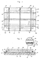
- Figur 1 shows the plan view which profiles an example of structure of the surface discharge type gas discharge panel of the present invention.
- Figur 2 is the sectional view along the Line II-II' of Fig. 1 .
- Figure 3 is the sectional view indicating an example of modification of the present invention.
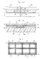
- Figure 4 is the plan view of the panel indicating an example of modification of the present invention where nine sheets (3 x 3 = 9) of electrode supporting substrates are combined.
- Figure 5 A and B are the plan view and the sectional view indicating the electrode connecting structure for obtaining a continuity of electrodes in the same order of the adjacent electrode supporting substrates.
- Figure 6 is the plan view of a panel indicating an example of modification of the present invention where eight sheets (2 x 4 = 8) of electrode supporting substrates are combined.
- Figure 7A, B, and C are the plan view and the sectional view indicating the electrode Leadout structure which is effective when used in the embodiment of Fig. 6.
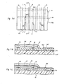
- Figure 8 and Figure 9 are the sectional views of a panel which realizes a color conversion or multi-color display of the present invention.
- In Fig. 1 and Fig. 2, the
display panel 10 is basically composed of the flat type,hermeticaLLy sealed body consisting of a pair of Largesize glass substrates discharge gas space 11. The one (upper)glass substrate 13 which functions as the cover substrate has the single plate structure, while the other (Lower)glass substrate 12 which functions as the electrode supporting substrate has the structure that four sheets ofglass substrates such substrate 12 is called hereafter"the combination substrate". - Said four
glass substrates Y electrodes 14 extending in the horizontal direction and also provide thereon a plurality ofX electrodes 15 extending in the vertical direction via the evaporatedinsulating film 15 consisting of the borosilicate glass. On theseX electrodes 16, thedielectric Layer 17 consisting of the borosilicate glass or evaporated film such as aluminium oxide etc. is provided and moreover it is covered with the surface Layer consisting of the evaporated film of magnesium oxide (Mg0) which is not illustrated. The one end of the Y electrode group and X electrode group of said respective substrate is respectively aligned so that the pertinent electrodes are arranged in the Line bridging over the adjacent two substrates, as indicated below, and moreover the other end is respectively exposed to the outside so that it becomes the connecting terminal for the external drive circuit. - The X electrodes and Y electrodes on the two sheets of substrate arranged on the same Line can be used respectively as a single X electrode and Y electrode when they are electrically connected at the inside or outside of the panel, or they can be used as an electrode having an independent function. Said Y,
X electrodes seal material 18 consisting of a Low melting point glass etc. is provided at the circumference between theglass substrate 13 for covering and thecombination substrate 12, and the mixed gas of Xe-He is supplied through thechip pipe 19 andexhaust port 20 and filled in the sealedgas space 11. - MeanwhiLe, a Large
size supporting substrate 21 for reinforcing the panel is arranged at the Lower side of saidcombination substrate 12. Moreover the Lowmelting point glass 22 to be used for bonding purpose is also provided at the circumference and the corresponding areas of aligning portion of saidelectrode supporting substrates 121 to 124 on said supportingsubstrate 21 and this bondingmaterial 22 realizes the junction for combining the four sheets of electrode supporting substrates and the aggregation between thepertinent combination substrate 12 and the supportingsubstrate 21. Here 23 is the through hole for accepting saidchip pipe 19. A method of assembling such a Large size display panel will be explained briefly as an example. - First, four sheets of
electrode supporting substrates substrate 21 which previously provides thebonding material 22 at the specified positions with the adjacent side edge surfaces aligned face to face. At this time, the aligning portion of said four sheets of electrode supporting substrate is Located on said bondingmaterial 22, while thechip pipe 19 is inserted in the throughhole 23, respectively. Thereafter, thesealing material 18 and the adequate spacer (not iLLustrated) are provided on the four sheets of the electrode supporting substrate, namely on thecombination substrate 12, and moreover thecovering glass substrate 13 is provided thereon. When adequate pressure and heat are applied on this stacking structure body, thebonding material 22 and the sealingmaterial 18 are respectively melted, thereby bonding (junction) the pertinent substrates and sealing thegas space 11. Thereafter, the discharge gas is supplied into thegas space 11 through thechip pipe 19, thereby completing the desired Large size, surface discharge type, gas discharge display panel. - Such a Large size display panel can be driven as explained below. NameLy, the matrix address drive at the entire part of thepanel becomes possible by electrically connecting the electrodes on the same Line of the adjacent two sheets of the electrode supporting substrates at the outside, and in the case that the electrodes are not electrically connected between the electrode substrates, the partial matrix address drive for each electrode supporting substrate becomes possible. In the former case, the drive circuit can be simplified and in the Latter case, the drive circuit is complicated but the high speed address indication can be attained. The basic embodiment of the present invention is explained above but the subject matter of the present invention is not Limited only to this embodiment and allows diversified modification and expansion. The modification examples can be Listed as follows.
- 1) The supporting substrate for reinforcing the panel described above is not always required. However, if it is not used, a thick electrode supporting substrate should be used. In addition, the Low-meLting point glass must be provided for the bonding purpose at the aligning portion of substrates (between the side edge surfaces). This bonding structure can also be adopted in case the supporting substrate for the panel reinforcement is used.
- 2) The electrodes and dielectric Layers can be formed not only by said thin film technique but also by the thick film technique.
- 3) In the case of the panel structure utilizing said supporting
substrate 21 for panel reinforcement, the chip pipe 19' can be provided on said supportingsubstrate 21 as shown in the sectional view of Fig. 3 by hermeticaLLy sealing the circumference of thecombination substrate 12 to the supportingsubstrate 21. In Fig. 3, the portion given thenumbering 191 is the low-melting-point glass for bonding the chip pipe 19' to the supportingsubstrate 21. According to this panel structure, the space between thecombination substrate 12 and the supportingsubstrate 21 is set to the same pneumatic pressure condition as the discharge gas filledspace 11. Therefore, there is no fear of deforming saidcombination substrate 12 due to the external pneumatic pressure on the occasion of the baking after exhausting the pressure from the gas filledspace 11 or at the time of actual display operation. For this reason, this method has the following merits that the gap of the gas filledspace 11 can be kept constant and the weight of panel as a whole can be reduced because a thin and Light weight material can be used for the electrode supporting substrate which configurates the-combination substrate 12. The practical values can be adopted as follows. The electrode supporting substrate in the size of 20 x 20 = 400 cm2 requires the thickness of 5 mm for the panel structure shown in Fig. 1 and Fig. 2, but the sufficient thickness is 1 mm in the case of the structure shown in Fig. 3. In the case of employing the chip pipe structure, it is necessary to allow the discharge gas to mutually flow between the pertinent electrode supporting substrate and the supporting substrate for reinforcement by providing the gas route to the bondingmaterial 22 which realizes the joint between the aligning portions of the electrode supporting substrates. Moreover, the circumference of the panel must be sealed under the condition that the side edges of the electrode supporting substrates are hermetically sealed and in this case more reliable sealing between the electrode supporting substrate edges can be obtained as the electrode supporting substrate is thinner. However, it is no Longer necessary to consider the sealing between the electrode supporting substrates when the structure, where the supportingsubstrate 21 and the circumference of thecover substrate 13 are directly sealed and thecombination substrate 12 is installed in the airtight space there between, is employed. - 4) The number of sheets of electrode supporting substrates combined is not Limited to the four explained above and more sheets of substrate can also be used.
- Figur 3 shows an example where nine sheets (3 x 3 = 9) of substrates are combined. In this case, the electrodes of five sheets of
substrates square substrates - Recommended as the first method is that the electrodes Located on the same Line bridging over the adjacent substrates are electrically connected via the connecting wires by the well known bonding technique under the condition that these substrates are arranged face to face.
- As the second wiring method, the wiring shown in Fig. 5A, B is recommended. NameLy, Fig. 5A shows the plan view of the major portion indicating the connecting structure of the
Y electrodes 14 on the same Line of the adjacent two sheets of theelectrode supporting substrates holes electrode Leadout conductors Y electrode 14 is formed. In this case, as shown in Fig. 5, the edge of the Y electrode is stacked at the one end of said electrode Leadout conductor and is electrically connected. Thereafter, the evaporatedfilm 15 of the borosilicate glass is formed on the surface of the ceramic substrate. Succeedingly, the X electrode and its Leadout conductor, although they are not illustrated, are formed by the above mentioned production method. The above mentionedelectrode supporting substrates 124, 128' are completed through the aforementioned production processes. Thus, such electrode supporting substrates are combined in the next step on the supporting substrate - 21 for reinforcement with the edge surfaces where theelectrode Leadout conductors substrate 21 for reinforcement. Theelectrode Leadout conductors conductor 31 consisting of the printed conductor paste. Thereafter, such a conductor is baked and melted. Thereby, bothconductors - According to the electrode connecting structure shown in Fig. 5 explained above, the electrodes in the same sequence on the same Line of the Y and
X electrodes electrode supporting substrates - As the third wiring method, the method effective for producing a rectangular Large size panel, which is composed of combined electrode supporting substrates arranged in two columns in thewertical direction as shown in Fig. 6, will be explained. NameLy, this method is characterized in that the
electrode supporting substrates electrode supporting substrates electrode supporting substrate 126 employing this method, while Fig. 7B and C respectively show the sectional views along the Lines I-I' and II-II' of Fig. 7A. In these figures, 1261 is the through hole; 141 is the electrode Leadout conductor consisting of the Au paste for connecting theY electrode 14 to the external drive circuit. - For said
electrode supporting substrates 121 to 128, the alumina ceramic material is used, and said through hole (1261) and said electrode Leadout conductor (141) of this ceramic substrate are formed by the method shown in Fig. 5. - 5) A Larger display panel can also be configurated by combining a plurality of Large size gas discharge panels shown in Fig. 1, Fig. 4, and Fig. 6. In this case, it is recommended for the method of combining the discrete panels to refer to the method described in the aforementioned U.S. patent no. 3,886,390.
- The examples of the expansion of this invention are Listed below.
- 1) The color conversion or the multi-color display can be realized by providing the ultra-violet rays activation type fluorescent material having the specified display color within the gas filled space of the panel or at the outside of the panel. Three practical examples thereof will be explained. NameLy, in the case of the first embodiment, the
fluorescent material 24 is provided at the internal surface of the coveringglass substrate 13 as shown in Fig. 2. In this case, it is only required that the fluorescent material having the specified display color is formed on the entire portion of the internal wall of said substrate, if the panel is the single color display panel only intended to the color conversion. In addition, it is required for the panel being intended for the multi-color display that the fluorescent material which partially shows the display of blue, red and green is provided as required in said internal surface of the substrates respectively corresponding to the display areas being composed of the intersecting points of theY electrode group 14 andX electrode group 16. The embodiment shown in Fig. 2 uses the mixed gas of Xe and He as the display gas and therefore (Y·Gd)BO3: Eu is recommended as the fluorescent material for the display in red, while BaMgAl14023:Eu for the display in blue and Zn2SiO4:Eu for the display in green respectively are recommended. - In the second embodiment, as shown in the sectional view of Fig. 8, the fluorescent material supporting substrates'41, 42, 43 ... in the size of 18 x 18 = 324 cm2 and in the thickness of 1 mm and in the same number as the combined electrode supporting substrates are also combined and arranged in the discharge gas filled space of the panel with the specified gap (0,1 mm) provided between the electrode supporting substrate. The
fluorescent material 24 of said fluorescent material supporting substrate can be formed by the procedures explained previously. - The
portion 51 is the spacer and 52 is the bonding material. This embodiment provides a Large merit that the Large scale facility is not required for the processing of the fluorescent material for providing the Large size multi-color display panel. As shown in the sectional view of Fig. 9, the third embodiment has the structure that the Large size fluorescentmaterial supporting substrates 61 forming thefluorescent material 24 are arranged face to face at the external wall surface of said coveringglass substrate 13. In short, the fluorescent material is provided at the external side of the panel and in this case sufficient consideration must be paid for the Light emitting efficiency of the fluorescent material, the prevention of the optical crosstalk between the Light emitting points and the humidity proof of the fluorescent material. - As the countermeasures, in the case of this embodiment, from the viewpoint of materials, the mixed gas of Ar + N2 is used as the discharge gas, a glass material of corning 9-54, 9700 produced by Corning Corp. in the thickness of 1mm is used as the glass substrate for covering, while YO2S:Eu , ZnS:Ag, ZnS:Cu-AL as the fluorescent material, respectively, are used. Then, from the viewpoint of the structure, as shown in Fig. 9, the bored insulating
substrate 62 for obtaining an independent discharge area is provided in the gas filledspace 11, simultaneously the circumference of said fluorescentmaterial supporting substrate 61 is sealed by thefrit material 63 and the dry gas is filled into the sealed space between saidsubstrate 61 and the coveringglass substrate 13. For said fluorescentmaterial supporting substrate 61, a comparatively thick glass substrate of 2 mm is used and this substrate shows the effect of reinforcing said coveringglass substrate 13 in combination with said bored insulatingsubstrate 62. This embodiment allows the fluorescent material to be provided after the completion of panel, following the assembling of the electrode supporting substrates and covering glass substrates and resuLtingLy offers the advantage that the flexibility of panel for the demand of display color increases. It is required to provide the pertinent fluorescent material only for the completed panel and therefore the production yield of multi-color display panel can fantastically be improved. i Other expansion examples are also Listed below. - 2) As the applicable panel, not only the above mentioned matrix type but also the segment type self shift panel can be used.
- 3) As the electrode structure, the matrix type electrode structure proposed in the U.S. patent no. 4,164,678 can also be used in addition to the above mentioned double Layered structure. This electrode structure will be briefly explained below. The electrode pad having a floating structure which capacitively couples with the Lower Layer electrode (Y eLectrode) is provided at the position near to the single side of the upper Layer electrode (X eLectrode) and a discharge is caused at the area between said upper Layer electrode and the pertinent electrode pad. As it is obvious from the above explanation, the present invention is intended for a surface discharge type gas discharge panel which realizes a Large size display panel, and is characterized in that a plurality of small size electrode supporting substrates which can be produced comparatively easily with a high production yield is combined in such a form that the side edge surfaces of said substrates are aligned face to face and a single Large size cover substrate is also arranged face to face at the upper part of this combination substrate. Thereby, a Large size gas discharge display panel having a high production yield can be produced without requiring a Large scale production facility. Moreover, a Large size multi-color display panel can be obtained by providing the fluorescent material in the gas filled space specified by a pair of substrates arranged face to face or at the external wall surface of the substrate.
Claims (11)
Applications Claiming Priority (2)
| Application Number | Priority Date | Filing Date | Title |
|---|---|---|---|
| JP163712/80 | 1980-11-19 | ||
| JP55163712A JPS5787048A (en) | 1980-11-19 | 1980-11-19 | Gas discharge panel |
Publications (3)
| Publication Number | Publication Date |
|---|---|
| EP0052376A2 true EP0052376A2 (en) | 1982-05-26 |
| EP0052376A3 EP0052376A3 (en) | 1983-02-23 |
| EP0052376B1 EP0052376B1 (en) | 1987-02-11 |
Family
ID=15779198
Family Applications (1)
| Application Number | Title | Priority Date | Filing Date |
|---|---|---|---|
| EP81109741A Expired EP0052376B1 (en) | 1980-11-19 | 1981-11-17 | Gas discharge display panel |
Country Status (4)
| Country | Link |
|---|---|
| US (1) | US4697123A (en) |
| EP (1) | EP0052376B1 (en) |
| JP (1) | JPS5787048A (en) |
| DE (1) | DE3175921D1 (en) |
Families Citing this family (16)
| Publication number | Priority date | Publication date | Assignee | Title |
|---|---|---|---|---|
| KR940004290B1 (en) * | 1991-11-27 | 1994-05-19 | 삼성전관 주식회사 | Liquid crystal devices and making method of plasma address |
| JPH0637092U (en) * | 1992-10-27 | 1994-05-17 | ワン ソン−チン | Buffer folding bike |
| JPH0730192U (en) * | 1993-11-18 | 1995-06-06 | 水雲 林 | Foldable bicycle |
| US6710525B1 (en) | 1999-10-19 | 2004-03-23 | Candescent Technologies Corporation | Electrode structure and method for forming electrode structure for a flat panel display |
| US6620012B1 (en) | 2000-10-27 | 2003-09-16 | Science Applications International Corporation | Method for testing a light-emitting panel and the components therein |
| US6545422B1 (en) | 2000-10-27 | 2003-04-08 | Science Applications International Corporation | Socket for use with a micro-component in a light-emitting panel |
| US6570335B1 (en) * | 2000-10-27 | 2003-05-27 | Science Applications International Corporation | Method and system for energizing a micro-component in a light-emitting panel |
| US6822626B2 (en) | 2000-10-27 | 2004-11-23 | Science Applications International Corporation | Design, fabrication, testing, and conditioning of micro-components for use in a light-emitting panel |
| US6612889B1 (en) | 2000-10-27 | 2003-09-02 | Science Applications International Corporation | Method for making a light-emitting panel |
| US6801001B2 (en) * | 2000-10-27 | 2004-10-05 | Science Applications International Corporation | Method and apparatus for addressing micro-components in a plasma display panel |
| US6764367B2 (en) * | 2000-10-27 | 2004-07-20 | Science Applications International Corporation | Liquid manufacturing processes for panel layer fabrication |
| US6796867B2 (en) * | 2000-10-27 | 2004-09-28 | Science Applications International Corporation | Use of printing and other technology for micro-component placement |
| US7288014B1 (en) | 2000-10-27 | 2007-10-30 | Science Applications International Corporation | Design, fabrication, testing, and conditioning of micro-components for use in a light-emitting panel |
| US6762566B1 (en) | 2000-10-27 | 2004-07-13 | Science Applications International Corporation | Micro-component for use in a light-emitting panel |
| US6935913B2 (en) * | 2000-10-27 | 2005-08-30 | Science Applications International Corporation | Method for on-line testing of a light emitting panel |
| US20050189164A1 (en) * | 2004-02-26 | 2005-09-01 | Chang Chi L. | Speaker enclosure having outer flared tube |
Citations (4)
| Publication number | Priority date | Publication date | Assignee | Title |
|---|---|---|---|---|
| US3646384A (en) * | 1970-06-09 | 1972-02-29 | Ibm | One-sided plasma display panel |
| US3886390A (en) * | 1974-08-29 | 1975-05-27 | Burroughs Corp | Buttable, gaseous discharge, display panel including electrodes providing a dot matrix display |
| US4035689A (en) * | 1974-07-12 | 1977-07-12 | Burroughs Corporation | Panel-type display device |
| GB1570763A (en) * | 1976-02-06 | 1980-07-09 | Nippon Electric Kagoshima Ltd | Luminescent display panel |
Family Cites Families (1)
| Publication number | Priority date | Publication date | Assignee | Title |
|---|---|---|---|---|
| NL6909119A (en) * | 1969-06-13 | 1970-12-15 |
-
1980
- 1980-11-19 JP JP55163712A patent/JPS5787048A/en active Granted
-
1981
- 1981-11-09 US US06/319,404 patent/US4697123A/en not_active Expired - Lifetime
- 1981-11-17 DE DE8181109741T patent/DE3175921D1/en not_active Expired
- 1981-11-17 EP EP81109741A patent/EP0052376B1/en not_active Expired
Patent Citations (4)
| Publication number | Priority date | Publication date | Assignee | Title |
|---|---|---|---|---|
| US3646384A (en) * | 1970-06-09 | 1972-02-29 | Ibm | One-sided plasma display panel |
| US4035689A (en) * | 1974-07-12 | 1977-07-12 | Burroughs Corporation | Panel-type display device |
| US3886390A (en) * | 1974-08-29 | 1975-05-27 | Burroughs Corp | Buttable, gaseous discharge, display panel including electrodes providing a dot matrix display |
| GB1570763A (en) * | 1976-02-06 | 1980-07-09 | Nippon Electric Kagoshima Ltd | Luminescent display panel |
Also Published As
| Publication number | Publication date |
|---|---|
| DE3175921D1 (en) | 1987-03-19 |
| JPS5787048A (en) | 1982-05-31 |
| US4697123A (en) | 1987-09-29 |
| EP0052376B1 (en) | 1987-02-11 |
| EP0052376A3 (en) | 1983-02-23 |
| JPH0221093B2 (en) | 1990-05-11 |
Similar Documents
| Publication | Publication Date | Title |
|---|---|---|
| EP0052376B1 (en) | Gas discharge display panel | |
| US5747931A (en) | Plasma display and method of making same | |
| US5925203A (en) | Method of making a plasma display | |
| US5493175A (en) | Plasma display panel | |
| JPH0217899B2 (en) | ||
| KR20020095454A (en) | Plasma display panel and manufacturing method thereof | |
| KR100334168B1 (en) | Flat display panel | |
| KR100869109B1 (en) | Plasma display panel having alignment mark portion and the method for fabricating the same | |
| US20080129657A1 (en) | Plasma display panel | |
| US4725255A (en) | Gas discharge display device | |
| JPS5871534A (en) | Gas electric-discharge panel | |
| JPS6028099B2 (en) | Gas discharge type display device | |
| CN1178265C (en) | Plasma display with driver circuit installed on single surface and its manufacture method | |
| JP3032552B2 (en) | Plasma display panel | |
| JPS6178036A (en) | Fluorescent display tube | |
| JPS603487Y2 (en) | Fluorescent display tube substrate device | |
| JPH05225911A (en) | Plasma display panel | |
| JP2623405B2 (en) | Color plasma display panel | |
| JPS5873941A (en) | Gas electric-discharge panel | |
| JPH05159707A (en) | Color plasma display panel | |
| JPH05159706A (en) | Color plasma display panel | |
| JPH0495330A (en) | Gas electric discharge panel | |
| JPH034429A (en) | Gas discharge panel | |
| JPH01276537A (en) | Connection method of thin film and thick film conductors and plasma discharge emission apparatus | |
| JPH02144834A (en) | Fluorescent character display tube |
Legal Events
| Date | Code | Title | Description |
|---|---|---|---|
| PUAI | Public reference made under article 153(3) epc to a published international application that has entered the european phase |
Free format text: ORIGINAL CODE: 0009012 |
|
| AK | Designated contracting states |
Designated state(s): DE FR GB NL |
|
| PUAL | Search report despatched |
Free format text: ORIGINAL CODE: 0009013 |
|
| AK | Designated contracting states |
Designated state(s): DE FR GB NL |
|
| 17P | Request for examination filed |
Effective date: 19830630 |
|
| GRAA | (expected) grant |
Free format text: ORIGINAL CODE: 0009210 |
|
| AK | Designated contracting states |
Kind code of ref document: B1 Designated state(s): DE FR GB NL |
|
| ET | Fr: translation filed | ||
| REF | Corresponds to: |
Ref document number: 3175921 Country of ref document: DE Date of ref document: 19870319 |
|
| PLBE | No opposition filed within time limit |
Free format text: ORIGINAL CODE: 0009261 |
|
| STAA | Information on the status of an ep patent application or granted ep patent |
Free format text: STATUS: NO OPPOSITION FILED WITHIN TIME LIMIT |
|
| 26N | No opposition filed | ||
| PGFP | Annual fee paid to national office [announced via postgrant information from national office to epo] |
Ref country code: NL Payment date: 19921130 Year of fee payment: 12 |
|
| PG25 | Lapsed in a contracting state [announced via postgrant information from national office to epo] |
Ref country code: NL Effective date: 19940601 |
|
| NLV4 | Nl: lapsed or anulled due to non-payment of the annual fee | ||
| PGFP | Annual fee paid to national office [announced via postgrant information from national office to epo] |
Ref country code: FR Payment date: 19981110 Year of fee payment: 18 |
|
| PGFP | Annual fee paid to national office [announced via postgrant information from national office to epo] |
Ref country code: GB Payment date: 19981120 Year of fee payment: 18 Ref country code: DE Payment date: 19981120 Year of fee payment: 18 |
|
| PG25 | Lapsed in a contracting state [announced via postgrant information from national office to epo] |
Ref country code: GB Free format text: LAPSE BECAUSE OF NON-PAYMENT OF DUE FEES Effective date: 19991117 |
|
| GBPC | Gb: european patent ceased through non-payment of renewal fee |
Effective date: 19991117 |
|
| PG25 | Lapsed in a contracting state [announced via postgrant information from national office to epo] |
Ref country code: FR Free format text: LAPSE BECAUSE OF NON-PAYMENT OF DUE FEES Effective date: 20000731 |
|
| PG25 | Lapsed in a contracting state [announced via postgrant information from national office to epo] |
Ref country code: DE Free format text: LAPSE BECAUSE OF NON-PAYMENT OF DUE FEES Effective date: 20000901 |
|
| REG | Reference to a national code |
Ref country code: FR Ref legal event code: ST |