EP0061602B1 - A method of fabricating and testing a programmable integrated circuit before it is programmed - Google Patents
A method of fabricating and testing a programmable integrated circuit before it is programmed Download PDFInfo
- Publication number
- EP0061602B1 EP0061602B1 EP82101677A EP82101677A EP0061602B1 EP 0061602 B1 EP0061602 B1 EP 0061602B1 EP 82101677 A EP82101677 A EP 82101677A EP 82101677 A EP82101677 A EP 82101677A EP 0061602 B1 EP0061602 B1 EP 0061602B1
- Authority
- EP
- European Patent Office
- Prior art keywords
- diode
- circuit
- lines
- line
- decoder
- Prior art date
- Legal status (The legal status is an assumption and is not a legal conclusion. Google has not performed a legal analysis and makes no representation as to the accuracy of the status listed.)
- Expired
Links
Images

Classifications
-
- G—PHYSICS
- G11—INFORMATION STORAGE
- G11C—STATIC STORES
- G11C29/00—Checking stores for correct operation ; Subsequent repair; Testing stores during standby or offline operation
- G11C29/04—Detection or location of defective memory elements, e.g. cell constructio details, timing of test signals
- G11C29/08—Functional testing, e.g. testing during refresh, power-on self testing [POST] or distributed testing
- G11C29/12—Built-in arrangements for testing, e.g. built-in self testing [BIST] or interconnection details
- G11C29/18—Address generation devices; Devices for accessing memories, e.g. details of addressing circuits
- G11C29/24—Accessing extra cells, e.g. dummy cells or redundant cells
-
- G—PHYSICS
- G01—MEASURING; TESTING
- G01R—MEASURING ELECTRIC VARIABLES; MEASURING MAGNETIC VARIABLES
- G01R31/00—Arrangements for testing electric properties; Arrangements for locating electric faults; Arrangements for electrical testing characterised by what is being tested not provided for elsewhere
- G01R31/28—Testing of electronic circuits, e.g. by signal tracer
- G01R31/317—Testing of digital circuits
- G01R31/3181—Functional testing
- G01R31/3185—Reconfiguring for testing, e.g. LSSD, partitioning
- G01R31/318516—Test of programmable logic devices [PLDs]
-
- G—PHYSICS
- G11—INFORMATION STORAGE
- G11C—STATIC STORES
- G11C29/00—Checking stores for correct operation ; Subsequent repair; Testing stores during standby or offline operation
- G11C29/52—Protection of memory contents; Detection of errors in memory contents
-
- H—ELECTRICITY
- H03—ELECTRONIC CIRCUITRY
- H03K—PULSE TECHNIQUE
- H03K19/00—Logic circuits, i.e. having at least two inputs acting on one output; Inverting circuits
- H03K19/02—Logic circuits, i.e. having at least two inputs acting on one output; Inverting circuits using specified components
- H03K19/173—Logic circuits, i.e. having at least two inputs acting on one output; Inverting circuits using specified components using elementary logic circuits as components
- H03K19/177—Logic circuits, i.e. having at least two inputs acting on one output; Inverting circuits using specified components using elementary logic circuits as components arranged in matrix form
- H03K19/17704—Logic circuits, i.e. having at least two inputs acting on one output; Inverting circuits using specified components using elementary logic circuits as components arranged in matrix form the logic functions being realised by the interconnection of rows and columns
- H03K19/17708—Logic circuits, i.e. having at least two inputs acting on one output; Inverting circuits using specified components using elementary logic circuits as components arranged in matrix form the logic functions being realised by the interconnection of rows and columns using an AND matrix followed by an OR matrix, i.e. programmable logic arrays
Definitions
- This invention relates generally to semiconductor device circuits and more particularly to a method for fabricating and testing irreversible, programmed integrated circuits before they are irreversibly programmed, i.e. before permanent connections between working parts are formed.
- IBM Technical Disclosure Bulletin, Vol. 17, #1, June 1974, pp. 245-247, describes a memory system fabrication scheme using a laser to form connections in which the connections are formed through an overlying oxide layer without removal of a portion of the oxide layer so that metal lines on the surface of the oxide are connected to underlying, diffused signal tracks.
- the memory chips Prior to forming the connections the memory chips are tested. For this purpose additional test tracks and additional gates to switch in the memory chips to the test tracks are provided. After the testing phase good memory chips are interconnected to signal tracks by laser formed connections.
- U.S. Patent 3,801,910 issued April 2, 1974 to H.F. Quinn and assigned to the same assignee as is the present invention, discloses a method of using a photodiode to temporarily interconnect a selected circuit to a test point. Specifically, this patent teaches that by shining a light on a photodiode it can be made to conduct and temporarily cause a circuit to be connected to a test bus.
- these patents are similar to the teaching of U.S. Patent 3,801,910.
- Malmberg short circuits the diode by a selected metallization step with standard vapor or sputter deposition techniques.
- U.S. Patent 4,240,094 relates to a laser- configured logic array.
- an array of universal logic devices may be formed together with a matrix pattern of intrablock pathways through which the building blocks may be tested prior to logic design and selectively interconnected by laser formed connections.
- peripheral circuits such as latches or decoder circuits normally are partially or totally inoperable prior to the programming of the array and thus normally untestable until after the array has been programmed.
- IBM Technical Disclosure Bulletin, Vol. 22, #4, October 1979, pp. 1866-1869 relates to the pretesting of laserable PLA peripheral circuits. Additional test lines and test transistors are provided to connect the input lines of the decoder circuits to decoder test line input terminals which are laser-connectable to ground after testing. A resistor is included between the test transistors and these laser formed connections. Thus, many additional devices are needed to allow for the pretesting operation.
- the present invention permits the testing of such peripheral circuits prior to the programming of the associated logic array, at low costs.
- the method is used to test latch inputs to a decoder circuit.
- the invention allows the testing of the programmable circuit before it is programmed which facilitates testing and the indication of an error location.
- the testing is achieved by providing a diode as an input connection to the circuit which diode presents a defined differential resistance and is used only during the testing phase. After the testing, selected potential connection points are closed thereby connecting a resistor in parallel to the diode which allows to obtain, during normal operation, a selected input resistance to the circuit, mainly defined by the parallel connected resistor.
- the method according to the invention has the advantage that a first input resistance suitable for the testing phase can be selected during this testing phase and a second input resistance suitable for the operating phase of the circuit can be selected during this operating phase. To achieve this, no additional switching operation or device is needed because the closing of the connection points is performed by the same apparatus and during the same period of time as is needed for the programming, i.e. the personalization of the programmable circuit.
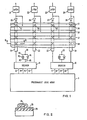
- Fig. 1 shows a block diagram of the latch and decoder inputs coupled to a programmable logic array prior to programming of the array.
- a programmable logic array 10 with two decoder circuits 11 and 12 coupled thereto via decoder output lines 13, 14, 15,16,17,18,19 and 20.
- Such decoder circuits are also known as 2 bit partitioner circuits.
- Each decoder is coupled in turn to a pair of input metal lines.
- decoder 11 is coupled to input metal lines 21 and 22 while decoder 12 is coupled to input metal lines 23 and 24.
- Each of these input metal lines is in turn coupled through a respective diode to a respective latch circuit.
- line 21 is connected via diode 25 to latch 31.
- the line 22 is connected via diode 26 to latch 32
- line 23 is coupled via diode 27 to latch 33
- line 24 is connected via diode 28 to latch 34.
- Additional electrically floating metal lines 35, 36,37 and 38 are deposited over but isolated from the metal lines 21, 22, 23 and 24 by an isolating layer 29. It should also be noted that these floating metal lines 35 through 38 are arranged orthogonal to the underlying metal lines 21 through 24. These floating metallic lines are provided between the latch circuits and the decoder circuits.
- each latch circuit there is one such orthogonal line there for each latch circuit and each is wired to a respective latch circuit.
- line 21 is connected to latch circuit 31 via diode 25 and the floating line 35 is coupled to the latch circuit 31 via a direct wire connection.
- line 22 is connected to the latch circuit 32 via the diode 26 while the floating line 36 is directly connected to the latch circuit 32.
- Line 23 is connected via the diode 27 to the latch circuit 33 while the floating line 37 is directly connected to the latch circuit 33.
- line 24 is connected to the latch circuit 34 via the diode 28 and the floating line 38 is directly connected to this latch circuit 34.
- Each decoder circuit is in turn coupled to a voltage source 39.
- the base of the decoder reference transistor 64 of decoder 11 as shown in Fig. 3 is connected to source 39 via a diode 41.
- This base of transistor 64 is also connected to a metal line 42 overlying but isolated from a second metal line 43 connected to the source 39.
- a box such as box 45 and referred to as a potential connection point.
- the reference transistor of the decoder 12 is similarly connected to source 39.
- the elements other than source 39 are not numbered since the detailed description of the interaction of but one decoder, i.e. decoder 11 given below with its respective latches 31 and 32 should suffice to clearly teach the present invention.
- diodes 25 and 26 to the lines leading from the latch to the decoder and the addition of the diode 41 between the base of the reference transistor 64 and the voltage source 39 of the decoder 11 permits balanced pre-programmed product terms to be applied to the decoder 11 so as to permit testing of the decoder 11 as well as the latches 31 and 32.
- the diodes 27 and 28 together with the diode connected between the base of the reference transistor in the decoder 12 and the source 39 permits testing of the decoder 12 and latches 33 and 34. Patterns generated by standard so-called stuck fault testing methods can be used to test the input latches and the decoder prior to the programming of the array 10. The utilization and introduction of such patterns into latches and decoders is well known to the art and need not be described herein.
- Latch 31 supplies a positive pulse, via diode 25 and line 21, to the base of transistor 50 of Fig. 3 which shows the decoder 11 in schematic detail. It will be assumed, for purposes of illustration only, that the latch 32 is off and not supplying a pulse through diode 26 to the line 22 which is connected to the base of transistor 51. In this instance the current flow through transistor 50 increases while the current flow through the transistor 51 whose base is connected to line 22 remains low. The imposition of one or both of these pulses via latches 31 and 32 to the bases of the respective transistors 50 and 51 causes the output lines 13, 14, 15 and 16 to rise or to remain at their respective level accordingly.
- each latch is permanently connected to a decoder input, i.e. one of the latches 31, 32, 33 or 34 by fusing together one of the lines 35, 36, 37 or 38 to one of the other underlying lines 21, 22, 23 or 24.
- latch 31 can be connected to any one of the lines by fusing the electrically floating line 35 at any one of the points 101, 102, 103, or 104. In this case it will be assumed that point 101 was selected, and the line 35 fused to the underlying line 21 and the output of the latch 31 would be supplied to the decoder 11.
- each latch can send directly via the diode connecting it to the decoder a signal suitable for testing of the decoder. Because of this diode coupling to the line before personalization diode 41 is added between the voltage source 39 and the decoder 11 in order to match the voltage drop of the diode 25 between the latch and the line during this pre-programming testing step.
- the diode i.e. diode 25 becomes ineffective and functionally out of the circuit and it becomes necessary to also functionally remove the diode 41 from the circuit. This is accomplished by fusing the lines 42 and 43 together at the indicated point 45. When the lines 42 and 43 become so fused the diode 41 is also functionally removed from the decoder circuit and is of no effect.
- the basic concept of the decoder circuit shown in Fig. 3 is well known and is basically a pair of emitter coupled switches.
- This decoder can be used either as a single bit position decoder or alternately as a two to four bit decoder and can be supplied with power proportioning.
- These operating characteristics can be selected by programming, as is subsequently described in order to facilitate understanding of the invention; although the invention itself is not concerned with the programming as such.
- one switch is comprised of switching transistors 52 and 53 and a common current transistor 54 while the second comprised of switching transistors 55 and 56 with a common current transistor 57.
- the transistor 52 has its base coupled through a diode 58 to the emitter of the input transistor 50 whose collector is coupled to source 39.
- the base of transistor 52 is also coupled to a current transistor 59 whose base is connected to a reference voltage REF. and to base of transistor 54.
- the emitter of transistor 59 is coupled through a resistor 60 to the emitter of the current transistor 54 and through a pair of resistors 61 and 62 to ground.
- the base of transistor 53 is coupled through a diode 63 to the emitter of a reference transistor 64 whose collector is coupled in common with the collector of transistor 50, and whose base is coupled to the source 39 via diode 41 and lines 42 and 43 via connection point 45.
- the base of transistor 53 is also coupled through a current transistor 66 whose base is in common with the bases of transistors 54 and 59 and whose emitter is coupled through a resistor 67 to the emitter of transistor 54.
- the collector of transistor 52 is coupled to the output line 13 through a diode 68.
- Line 13 is coupled through series resistors 69 and 70 to source 39.
- the collector of transistor 52 is also coupled via a diode 69 and via a potential connection point 72 to the line 14.
- This connection point 72 is formed by the line 72a and an overlying insulated line 72b.
- the lines 72a and 72b need only to be isolated, one from the other, by an insulation material where they overlap at point 72.
- the line 72b is also coupled directly to the output 14.
- the transistor 53 is similarly connected, i.e. it is directly coupled to the line 15 through diode 73 and through a diode 74 and a potential connection point formed of isolated lines 75a and 75b to the line 16.
- Transistors 55 and 56 are also common emitters coupled through a current transistor 57 whose emitter is coupled to ground through series resistors 76 and 77.
- the base of transistor 55 is coupled to the emitter of the transistor 64 through a diode 78 and to the collector of a current transistor 79 whose base is tied in common with transistors 54, 57, 59, 66 and 82.
- the emitter of transistor 79 is coupled through a resistor 80 to the emitter of transistor 57.
- the base of transistor 56 is coupled to the emitter of an input transistor 51 through a diode 81 and to the collector of a current transistor 82 whose emitter is coupled through a resistor 83 to the emitter of current transistor 57.
- the base of transistor 51 is of course coupled to line 22.
- the transistor 55 is connected to the line 14 through a diode 84 and the collector coupled via diode 85 and connection point 86 formed of lines 86a and 86b to the line 15. Again these lines are isolated one from the other at the point 86.
- the transistor 56 has its collector coupled via diode 87 to line 16 and via diode 88 and potential connection point 89 formed of isolated lines 89a and 89b to line 13.
- Line 14 is connected to source 39 via series resistors 90 and 91, line 15 via series resistors 92 and 93 and line 16 via series resistors 94 and 95. At least one resistor in each of these series is provided with a parallel potential connection point.
- the pairs of lines 72a, 72b, 75a, 75b, 86a, 86b and 89a and 89b forming the respective potential connection points 72, 75, 86 and 89 remain isolated one from the other by virtue of the isolation material between the lines.
- the circuit as shown is a single bit decoder and the output is accomplished with the respective current switches which direct the drive current into selected ones of the respective output lines 13 or 15 and 14 or 16.
- a selected output is one which has no current flowing therein. Consequently one line will be more positive than the other in each pair.
- the voltage levels with respect to ground of the input lines 21 and 22 determine which of the current sources will be conducting as is well known in the art.
- resistor 70 has a parallel connection point 70a which is formed by the overlying of isolated lines 70b and 70c.
- resistor 90 has a parallel connection point 90a which is formed by overlying isolated lines 90a, 90b and 90c.
- resistor 93 and 94 have similar connection points in parallel therewith, i.e.
- resistor 93 has a connection point 93a formed by lines 93b and 93c
- resistor 95 has a parallel connection point 95a formed by lines 95b and 95c.
- resistors 62 and 77 which also have parallel connection points.
- resistor 62 has a parallel connection point 62a formed of lines 62b and 62c
- resistor 77 has a parallel connection point 77a formed by lines 77b and 77c.
- junction point 70a were treated such as to remove the isolation between the lines 70b and 70c an effective short circuit would be formed around the resistor 70 and the resistor 70 would be removed from the circuit.
- decoders The operation of such decoders is well known in the art.
- connection points between the collector of the respective emitter coupled transistors and the output lines be treated so that whenever one of the emitter coupled transistors turns on both lines coupled to its collector will be selected.
- connection point 72 was treated so that lines 72a and 72b are directly connected then when transistor 52 turns on both line 13 and line 14 would be selected.
- connection points 72, 75, 86 and 89 to join the respective, necessary lines the unit can be made into a two to four bit decoder so that each of the respective emitter coupled transistors forming the two emitter coupled switches, i.e. transistors 52, 53, 55 and 56, will, when activated, select one of the output lines 13, 14, 15, 16.
- connection points 70a and 90a, 93a, 95a around each of respective ones of the series resistors coupled to the output lines power proportioning can be achieved so that the drive power levels to each of the array lines, i.e. to each of the output lines 13, 14, 15 and 16 can be made proportional to the loading of that individual line.
- the programming or treatment of all such interconnection points would of course be made at the same time.
- Program power proportioning of programmable logic arrays is generally described in Vol. 18, #4, September 1975 in the IBM Technical Disclosure Bulletin, on page 1048.
- both the programmable logic array and the decoder circuits can be tailored to achieve selective impedance characteristics in the circuit.
- latch inputs can be provided to the decoder prior to the actual programming of the logic array unit, since it provides an initial impedance line to the input of the decoder which impedance can be later effectively removed so that the actual unit can be programmed to a desired end result.
- the latch 31 which is coupled to line 21 through diode 25.
- the input of the latch can be provided to line 21 while the output of the latch 32 which is connected to line 22 can also be provided to the decoder 11 and to test the output of the decoder at lines 13, 14, 15 and 16.
- various combinations of series and parallel resistors together with either serial or parallel connection points even greater latitude can be achieved in tailoring impedances in a circuit.
- the technique can be used with other circuit elements both active and passive.
- a diode is in parallel with a 500 ohm resistor in series with a connection point. If we assume that the current flow through the circuit is 0.1 m amps then before the connection point is fused all the current is flowing through the diode and the circuit has an apparent (small signal) impedance of 260 ohms. After fusion of the connection point the diode effectively drops out of the circuit and the impedance of the circuit is that of the resistor, i.e. 500 ohms. Thus, the resultant impedance of the circuit increases over that of the diode alone.
- example 1 The circuit of example 1 is again assumed. In this case however, only 0.01 m amps is assumed to be flowing through the circuit. At this current level, the impedance of the diode appears to be 2600 ohms.
- the diode When the connection point is fused the diode effectively drops out of the circuit and the impedance of the circuit is 500 ohms, the value of the resistor. Thus, the resultant impedance of the circuit is lowered below that of the diode alone.
- the diode, resistor and connection point combination set above is again assumed. In this case however, it will be assumed that the resistor has a value of 100 ohms and the current drawn through the circuit is 0.1 m amps. Before fusion of the connection point the diode, at this current flow, appears to have an impedance of 260 ohms. After fusion the connection point the diode effectively drops out of the circuit and the resultant impedance of the circuit is that of the resistor, i.e. 100 ohms. Thus, the resultant impedances of the circuit is lowered below that of the diode alone.
- Such tailoring of the circuit of figure 1 could be accomplished for example by forming resistors in parallel with each of the diodes 25, 26, 27 and 28 or for example by forming the floating lines 35, 36, 37 and 38 of doped polysilicon so as to have a tailored resistance per unit length of line.
- connection points formed of overlying aluminum lines about 1 micron to 1.2 microns thick with a layer of silicon dioxide 2 microns thick therebetween.
- Each connection point should be about 14 micron square.
Description
- This invention relates generally to semiconductor device circuits and more particularly to a method for fabricating and testing irreversible, programmed integrated circuits before they are irreversibly programmed, i.e. before permanent connections between working parts are formed.
- IBM Technical Disclosure Bulletin, Vol. 17, #1, June 1974, pp. 245-247, describes a memory system fabrication scheme using a laser to form connections in which the connections are formed through an overlying oxide layer without removal of a portion of the oxide layer so that metal lines on the surface of the oxide are connected to underlying, diffused signal tracks. Prior to forming the connections the memory chips are tested. For this purpose additional test tracks and additional gates to switch in the memory chips to the test tracks are provided. After the testing phase good memory chips are interconnected to signal tracks by laser formed connections.
- U.S. Patent 3,801,910 issued April 2, 1974 to H.F. Quinn and assigned to the same assignee as is the present invention, discloses a method of using a photodiode to temporarily interconnect a selected circuit to a test point. Specifically, this patent teaches that by shining a light on a photodiode it can be made to conduct and temporarily cause a circuit to be connected to a test bus.
- U.S. Patent 4,140,967 issued February 20, 1979 to B.S. Balasubramanian et al and assigned to the same assignee as the present invention, discloses a programmable logic array and a method of testing it after it is programmed.
- U.S. Patent 4,233,671 issued November 11, 1980 to L. Gerzberg et al, discloses read-only memory and integrated circuits and a method of programming them by laser means.
- U.S. Patent 3,956,698 issued May 11, 1976 to P. R. Malmberg et al and its continuation-in-part U.S. Patent 4,053,833 issued October 11, 1977, discloses a method for testing an integrated circuit by switching on a diode. Thus, these patents are similar to the teaching of U.S. Patent 3,801,910. Subsequently, Malmberg short circuits the diode by a selected metallization step with standard vapor or sputter deposition techniques.
- U.S. Patent 4,240,094 relates to a laser- configured logic array. On the array chip, an array of universal logic devices may be formed together with a matrix pattern of intrablock pathways through which the building blocks may be tested prior to logic design and selectively interconnected by laser formed connections.
- In programmable logic arrays peripheral circuits such as latches or decoder circuits normally are partially or totally inoperable prior to the programming of the array and thus normally untestable until after the array has been programmed.
- IBM Technical Disclosure Bulletin, Vol. 22, #4, October 1979, pp. 1866-1869 relates to the pretesting of laserable PLA peripheral circuits. Additional test lines and test transistors are provided to connect the input lines of the decoder circuits to decoder test line input terminals which are laser-connectable to ground after testing. A resistor is included between the test transistors and these laser formed connections. Thus, many additional devices are needed to allow for the pretesting operation.
- The present invention permits the testing of such peripheral circuits prior to the programming of the associated logic array, at low costs.
- It is thus an object of the present invention to provide a means for testing such normally untestable circuits prior to programming of the array with which they are associated.
- It is a further object of the invention to provide a means whereby the testing means is functionally eliminated by using the same means that is used to program the array.
- It is another object of the present invention to provide means whereby the programming of the circuit also results in tailoring of the final impedance characteristics of the circuit.
- It is still another object of the invention to provide a circuit which can be programmed to have either increased or decreased impedance characteristics.
- These objects are achieved by a method as claimed in claim 1.
- In one embodiment the method is used to test latch inputs to a decoder circuit.
- The invention allows the testing of the programmable circuit before it is programmed which facilitates testing and the indication of an error location. The testing is achieved by providing a diode as an input connection to the circuit which diode presents a defined differential resistance and is used only during the testing phase. After the testing, selected potential connection points are closed thereby connecting a resistor in parallel to the diode which allows to obtain, during normal operation, a selected input resistance to the circuit, mainly defined by the parallel connected resistor. Thus the method according to the invention has the advantage that a first input resistance suitable for the testing phase can be selected during this testing phase and a second input resistance suitable for the operating phase of the circuit can be selected during this operating phase. To achieve this, no additional switching operation or device is needed because the closing of the connection points is performed by the same apparatus and during the same period of time as is needed for the programming, i.e. the personalization of the programmable circuit.
- The invention and objects and features thereof will be readily understood from the following detailed description when taken with the accompanying drawings herein:
- Fig. 1 is a block diagram showing the arrangement necessary to pretest the latch and decoder inputs to a programmable logic array prior to programming of the array in accordance with the present invention when built in an integrated circuit form.
- Fig. 2 is a section of two of the crossed metal lines of Fig. 1.
- Fig. 3 is a schematic drawing of the decoder of Fig. 1.
- Reference should be simultaneously made to Figs. 1, 2 and 3.
- Fig. 1 shows a block diagram of the latch and decoder inputs coupled to a programmable logic array prior to programming of the array.
- Shown in the figure is a
programmable logic array 10 with twodecoder circuits 11 and 12 coupled thereto viadecoder output lines input metal lines decoder 12 is coupled toinput metal lines line 21 is connected viadiode 25 tolatch 31. Theline 22 is connected viadiode 26 tolatch 32,line 23 is coupled viadiode 27 tolatch 33 andline 24 is connected viadiode 28 tolatch 34. - Additional electrically floating
metal lines metal lines isolating layer 29. It should also be noted that these floating metal lines 35 through 38 are arranged orthogonal to theunderlying metal lines 21 through 24. These floating metallic lines are provided between the latch circuits and the decoder circuits. - Thus, there is one such orthogonal line there for each latch circuit and each is wired to a respective latch circuit. Thus,
line 21 is connected tolatch circuit 31 viadiode 25 and the floating line 35 is coupled to thelatch circuit 31 via a direct wire connection. Similarly,line 22 is connected to thelatch circuit 32 via thediode 26 while thefloating line 36 is directly connected to thelatch circuit 32.Line 23 is connected via thediode 27 to thelatch circuit 33 while thefloating line 37 is directly connected to thelatch circuit 33. Finally,line 24 is connected to thelatch circuit 34 via thediode 28 and thefloating line 38 is directly connected to thislatch circuit 34. - Each decoder circuit is in turn coupled to a
voltage source 39. As will be further described below the base of thedecoder reference transistor 64 of decoder 11 as shown in Fig. 3 is connected tosource 39 via adiode 41. This base oftransistor 64 is also connected to ametal line 42 overlying but isolated from asecond metal line 43 connected to thesource 39. For purposes of description the overlap of any such two metallic lines, such aslines source 39, will be designated by a box such asbox 45 and referred to as a potential connection point. - The reference transistor of the
decoder 12 is similarly connected tosource 39. However, the elements other thansource 39 are not numbered since the detailed description of the interaction of but one decoder, i.e. decoder 11 given below with itsrespective latches - The addition of the
diodes diode 41 between the base of thereference transistor 64 and thevoltage source 39 of the decoder 11 permits balanced pre-programmed product terms to be applied to the decoder 11 so as to permit testing of the decoder 11 as well as thelatches diodes decoder 12 and thesource 39 permits testing of thedecoder 12 andlatches array 10. The utilization and introduction of such patterns into latches and decoders is well known to the art and need not be described herein. - Latch 31 supplies a positive pulse, via
diode 25 andline 21, to the base oftransistor 50 of Fig. 3 which shows the decoder 11 in schematic detail. It will be assumed, for purposes of illustration only, that thelatch 32 is off and not supplying a pulse throughdiode 26 to theline 22 which is connected to the base oftransistor 51. In this instance the current flow throughtransistor 50 increases while the current flow through thetransistor 51 whose base is connected to line 22 remains low. The imposition of one or both of these pulses vialatches respective transistors output lines - During personalization of the chip each latch is permanently connected to a decoder input, i.e. one of the
latches lines underlying lines points underlying line 21 and the output of thelatch 31 would be supplied to the decoder 11. - When such a fusion occurs the latch thus becomes directly connected to the line to which it has been fused and the
diode 25 is effectively isolated since insufficient current will be sent to the diode and thediode 25 will not turn on. - In any event, prior to personalization, each latch can send directly via the diode connecting it to the decoder a signal suitable for testing of the decoder. Because of this diode coupling to the line before
personalization diode 41 is added between thevoltage source 39 and the decoder 11 in order to match the voltage drop of thediode 25 between the latch and the line during this pre-programming testing step. Once the array has been programmed and the correct floating line is welded by the laser or fused to the correct underlying line the diode, i.e.diode 25 becomes ineffective and functionally out of the circuit and it becomes necessary to also functionally remove thediode 41 from the circuit. This is accomplished by fusing thelines point 45. When thelines diode 41 is also functionally removed from the decoder circuit and is of no effect. - The basic concept of the decoder circuit shown in Fig. 3 is well known and is basically a pair of emitter coupled switches. This decoder can be used either as a single bit position decoder or alternately as a two to four bit decoder and can be supplied with power proportioning. These operating characteristics can be selected by programming, as is subsequently described in order to facilitate understanding of the invention; although the invention itself is not concerned with the programming as such.
- Of the two emitter coupled logic switches one switch is comprised of switching
transistors 52 and 53 and a commoncurrent transistor 54 while the second comprised of switchingtransistors current transistor 57. Thetransistor 52 has its base coupled through adiode 58 to the emitter of theinput transistor 50 whose collector is coupled tosource 39. The base oftransistor 52 is also coupled to acurrent transistor 59 whose base is connected to a reference voltage REF. and to base oftransistor 54. The emitter oftransistor 59 is coupled through aresistor 60 to the emitter of thecurrent transistor 54 and through a pair ofresistors diode 63 to the emitter of areference transistor 64 whose collector is coupled in common with the collector oftransistor 50, and whose base is coupled to thesource 39 viadiode 41 andlines connection point 45. The base of transistor 53 is also coupled through acurrent transistor 66 whose base is in common with the bases oftransistors resistor 67 to the emitter oftransistor 54. - The collector of
transistor 52 is coupled to theoutput line 13 through adiode 68.Line 13 is coupled throughseries resistors source 39. The collector oftransistor 52 is also coupled via adiode 69 and via apotential connection point 72 to theline 14. Thisconnection point 72 is formed by theline 72a and an overlyinginsulated line 72b. Thelines point 72. Theline 72b is also coupled directly to theoutput 14. The transistor 53 is similarly connected, i.e. it is directly coupled to theline 15 through diode 73 and through adiode 74 and a potential connection point formed ofisolated lines line 16. -
Transistors current transistor 57 whose emitter is coupled to ground throughseries resistors transistor 55 is coupled to the emitter of thetransistor 64 through a diode 78 and to the collector of acurrent transistor 79 whose base is tied in common withtransistors transistor 79 is coupled through aresistor 80 to the emitter oftransistor 57. The base oftransistor 56 is coupled to the emitter of aninput transistor 51 through adiode 81 and to the collector of acurrent transistor 82 whose emitter is coupled through aresistor 83 to the emitter ofcurrent transistor 57. The base oftransistor 51 is of course coupled toline 22. - The
transistor 55 is connected to theline 14 through adiode 84 and the collector coupled viadiode 85 andconnection point 86 formed oflines 86a and 86b to theline 15. Again these lines are isolated one from the other at thepoint 86. Similarly, thetransistor 56 has its collector coupled viadiode 87 toline 16 and viadiode 88 andpotential connection point 89 formed ofisolated lines 89a and 89b toline 13. -
Line 14 is connected to source 39 viaseries resistors line 15 viaseries resistors line 16 viaseries resistors - The pairs of
lines - The circuit as shown is a single bit decoder and the output is accomplished with the respective current switches which direct the drive current into selected ones of the
respective output lines example resistor 70 has a parallel connection point 70a which is formed by the overlying ofisolated lines resistor 90 has aparallel connection point 90a which is formed by overlyingisolated lines resistor resistor 93 has a connection point 93a formed bylines 93b and 93c, whileresistor 95 has a parallel connection point 95a formed bylines resistors resistor 62 has a parallel connection point 62a formed oflines resistor 77 has aparallel connection point 77a formed bylines lines resistor 70 and theresistor 70 would be removed from the circuit. The operation of such decoders is well known in the art. - Now in the case where a two to four bit decoder is desired it is necessary that the connection points between the collector of the respective emitter coupled transistors and the output lines be treated so that whenever one of the emitter coupled transistors turns on both lines coupled to its collector will be selected. Thus, for example if
connection point 72 was treated so thatlines transistor 52 turns on bothline 13 andline 14 would be selected. By selectively treating the connection points 72, 75, 86 and 89 to join the respective, necessary lines the unit can be made into a two to four bit decoder so that each of the respective emitter coupled transistors forming the two emitter coupled switches, i.e.transistors output lines - By providing
connection points 70a and 90a, 93a, 95a around each of respective ones of the series resistors coupled to the output lines power proportioning can be achieved so that the drive power levels to each of the array lines, i.e. to each of theoutput lines latch 31 which is coupled toline 21 throughdiode 25. The input of the latch can be provided toline 21 while the output of thelatch 32 which is connected to line 22 can also be provided to the decoder 11 and to test the output of the decoder atlines - One can easily tailor the impedance of any line by selection of circuit elements. For example if we consider a simple circuit comprised of a diode in parallel with a series combination of a resistor and a connection point then by either selecting the current through the circuit or by controlling the value of the resistor, the final resultant impedance of the circuit, after fusion of the connection point can be either higher or lower than that of the diode alone.
- A diode is in parallel with a 500 ohm resistor in series with a connection point. If we assume that the current flow through the circuit is 0.1 m amps then before the connection point is fused all the current is flowing through the diode and the circuit has an apparent (small signal) impedance of 260 ohms. After fusion of the connection point the diode effectively drops out of the circuit and the impedance of the circuit is that of the resistor, i.e. 500 ohms. Thus, the resultant impedance of the circuit increases over that of the diode alone.
- The circuit of example 1 is again assumed. In this case however, only 0.01 m amps is assumed to be flowing through the circuit. At this current level, the impedance of the diode appears to be 2600 ohms.
- When the connection point is fused the diode effectively drops out of the circuit and the impedance of the circuit is 500 ohms, the value of the resistor. Thus, the resultant impedance of the circuit is lowered below that of the diode alone.
- The diode, resistor and connection point combination set above is again assumed. In this case however, it will be assumed that the resistor has a value of 100 ohms and the current drawn through the circuit is 0.1 m amps. Before fusion of the connection point the diode, at this current flow, appears to have an impedance of 260 ohms. After fusion the connection point the diode effectively drops out of the circuit and the resultant impedance of the circuit is that of the resistor, i.e. 100 ohms. Thus, the resultant impedances of the circuit is lowered below that of the diode alone.
- Such tailoring of the circuit of figure 1 could be accomplished for example by forming resistors in parallel with each of the
diodes lines - In actual use it has been found that a so-called nitrogen dye laser having a pulse width of 4 to 8 nanoseconds, a repetition rate of 50 hertz, a spot diameter of 5 microns and a power density of 108 watts/cm2 can be advantageously used to fuse connection points formed of overlying aluminum lines about 1 micron to 1.2 microns thick with a layer of
silicon dioxide 2 microns thick therebetween. Each connection point should be about 14 micron square.
Claims (4)
Applications Claiming Priority (2)
| Application Number | Priority Date | Filing Date | Title |
|---|---|---|---|
| US248646 | 1981-03-27 | ||
| US06/248,646 US4404635A (en) | 1981-03-27 | 1981-03-27 | Programmable integrated circuit and method of testing the circuit before it is programmed |
Publications (2)
| Publication Number | Publication Date |
|---|---|
| EP0061602A1 EP0061602A1 (en) | 1982-10-06 |
| EP0061602B1 true EP0061602B1 (en) | 1986-02-05 |
Family
ID=22940026
Family Applications (1)
| Application Number | Title | Priority Date | Filing Date |
|---|---|---|---|
| EP82101677A Expired EP0061602B1 (en) | 1981-03-27 | 1982-03-04 | A method of fabricating and testing a programmable integrated circuit before it is programmed |
Country Status (4)
| Country | Link |
|---|---|
| US (1) | US4404635A (en) |
| EP (1) | EP0061602B1 (en) |
| JP (1) | JPS57166044A (en) |
| DE (1) | DE3268910D1 (en) |
Families Citing this family (22)
| Publication number | Priority date | Publication date | Assignee | Title |
|---|---|---|---|---|
| DE3220302C2 (en) * | 1982-05-28 | 1984-03-15 | Siemens AG, 1000 Berlin und 8000 München | Programmable logic arrangement in ECL technology |
| US4590581A (en) * | 1983-05-09 | 1986-05-20 | Valid Logic Systems, Inc. | Method and apparatus for modeling systems of complex circuits |
| US4937770A (en) * | 1986-02-07 | 1990-06-26 | Teradyne, Inc. | Simulation system |
| US4744084A (en) * | 1986-02-27 | 1988-05-10 | Mentor Graphics Corporation | Hardware modeling system and method for simulating portions of electrical circuits |
| NL8700933A (en) * | 1987-04-21 | 1988-11-16 | Philips Nv | TEST METHOD FOR LCD ELEMENTS. |
| US5081590A (en) * | 1988-02-29 | 1992-01-14 | Westinghouse Electric Corp. | Computer aided technique for post production tuning of microwave modules |
| US4937475B1 (en) * | 1988-09-19 | 1994-03-29 | Massachusetts Inst Technology | Laser programmable integrated circuit |
| US5109353A (en) | 1988-12-02 | 1992-04-28 | Quickturn Systems, Incorporated | Apparatus for emulation of electronic hardware system |
| US5329470A (en) * | 1988-12-02 | 1994-07-12 | Quickturn Systems, Inc. | Reconfigurable hardware emulation system |
| US4969124A (en) * | 1989-03-07 | 1990-11-06 | National Semiconductor Corporation | Method for vertical fuse testing |
| US5353243A (en) * | 1989-05-31 | 1994-10-04 | Synopsys Inc. | Hardware modeling system and method of use |
| US5369593A (en) * | 1989-05-31 | 1994-11-29 | Synopsys Inc. | System for and method of connecting a hardware modeling element to a hardware modeling system |
| US5680583A (en) * | 1994-02-16 | 1997-10-21 | Arkos Design, Inc. | Method and apparatus for a trace buffer in an emulation system |
| US5440246A (en) * | 1994-03-22 | 1995-08-08 | Mosel Vitelic, Incorporated | Programmable circuit with fusible latch |
| US5732246A (en) * | 1995-06-07 | 1998-03-24 | International Business Machines Corporation | Programmable array interconnect latch |
| US5651013A (en) * | 1995-11-14 | 1997-07-22 | International Business Machines Corporation | Programmable circuits for test and operation of programmable gate arrays |
| US5841967A (en) * | 1996-10-17 | 1998-11-24 | Quickturn Design Systems, Inc. | Method and apparatus for design verification using emulation and simulation |
| US5889414A (en) * | 1997-04-28 | 1999-03-30 | Mosel Vitelic Corporation | Programmable circuits |
| US5960191A (en) | 1997-05-30 | 1999-09-28 | Quickturn Design Systems, Inc. | Emulation system with time-multiplexed interconnect |
| US5970240A (en) * | 1997-06-25 | 1999-10-19 | Quickturn Design Systems, Inc. | Method and apparatus for configurable memory emulation |
| US6084803A (en) * | 1998-10-23 | 2000-07-04 | Mosel Vitelic, Inc. | Initialization of non-volatile programmable latches in circuits in which an initialization operation is performed |
| US6163492A (en) | 1998-10-23 | 2000-12-19 | Mosel Vitelic, Inc. | Programmable latches that include non-volatile programmable elements |
Family Cites Families (13)
| Publication number | Priority date | Publication date | Assignee | Title |
|---|---|---|---|---|
| US3772595A (en) * | 1971-03-19 | 1973-11-13 | Teradyne Inc | Method and apparatus for testing a digital logic fet by monitoring currents the device develops in response to input signals |
| US3815025A (en) * | 1971-10-18 | 1974-06-04 | Ibm | Large-scale integrated circuit testing structure |
| US3801910A (en) * | 1972-07-03 | 1974-04-02 | Ibm | Externally accessing mechanical difficult to access circuit nodes using photo-responsive conductors in integrated circuits |
| US3789205A (en) * | 1972-09-28 | 1974-01-29 | Ibm | Method of testing mosfet planar boards |
| US3787810A (en) * | 1972-11-02 | 1974-01-22 | Burroughs Corp | Test method for a programmable data communication terminal |
| US4053833A (en) * | 1974-02-12 | 1977-10-11 | Westinghouse Electric Corporation | Contactless test method for integrated circuits |
| US3956698A (en) * | 1974-02-12 | 1976-05-11 | Westinghouse Electric Corporation | Contactless test method for integrated circuits |
| US3958110A (en) * | 1974-12-18 | 1976-05-18 | Ibm Corporation | Logic array with testing circuitry |
| US4140967A (en) * | 1977-06-24 | 1979-02-20 | International Business Machines Corporation | Merged array PLA device, circuit, fabrication method and testing technique |
| JPS5487189A (en) * | 1977-12-23 | 1979-07-11 | Fujitsu Ltd | Test method for lsi |
| US4240094A (en) * | 1978-03-20 | 1980-12-16 | Harris Corporation | Laser-configured logic array |
| EP0011974B1 (en) * | 1978-11-25 | 1984-02-15 | Fujitsu Limited | Programmable memory device provided with test means |
| US4233671A (en) * | 1979-01-05 | 1980-11-11 | Stanford University | Read only memory and integrated circuit and method of programming by laser means |
-
1981
- 1981-03-27 US US06/248,646 patent/US4404635A/en not_active Expired - Lifetime
- 1981-12-18 JP JP56203782A patent/JPS57166044A/en active Granted
-
1982
- 1982-03-04 DE DE8282101677T patent/DE3268910D1/en not_active Expired
- 1982-03-04 EP EP82101677A patent/EP0061602B1/en not_active Expired
Also Published As
| Publication number | Publication date |
|---|---|
| JPH028663B2 (en) | 1990-02-26 |
| US4404635A (en) | 1983-09-13 |
| EP0061602A1 (en) | 1982-10-06 |
| DE3268910D1 (en) | 1986-03-20 |
| JPS57166044A (en) | 1982-10-13 |
Similar Documents
| Publication | Publication Date | Title |
|---|---|---|
| EP0061602B1 (en) | A method of fabricating and testing a programmable integrated circuit before it is programmed | |
| JP2557160B2 (en) | Low voltage programmable storage element | |
| US5294846A (en) | Method and apparatus for programming anti-fuse devices | |
| US4896055A (en) | Semiconductor integrated circuit technology for eliminating circuits or arrays having abnormal operating characteristics | |
| US4910417A (en) | Universal logic module comprising multiplexers | |
| US5008855A (en) | Method of programming anti-fuse element | |
| CN1316744C (en) | Antifuse reroute of dies | |
| US5412594A (en) | Fuse trimming in plastic package devices | |
| KR100395186B1 (en) | Programmable Logic Devices with Validation Circuits That Classify Valid Closed, Valid Open, or Invalid Fuse Link States | |
| DE10312676A1 (en) | Multi-level non-volatile memory device | |
| EP0066729A1 (en) | Method of testing the operation of a programmable logic array | |
| US5659182A (en) | Three-terminal fuse | |
| US6529038B2 (en) | Antifuse programming method | |
| EP0074417B1 (en) | Procedure and circuit arrangement for checking a circuit which is integrated with a three-state driver, which is driven to high impedance by this circuit | |
| US5514980A (en) | High resolution circuit and method for sensing antifuses | |
| US5572458A (en) | Multi-level vROM programming method and circuit | |
| US5453696A (en) | Embedded fuse resistance measuring circuit | |
| DE4316283A1 (en) | Semiconductor memory device | |
| EP0173357B1 (en) | Binary circuit with selectable output polarity | |
| US6236225B1 (en) | Method of testing the gate oxide in integrated DMOS power transistors and integrated device comprising a DMOS power transistor | |
| EP0206102A2 (en) | Programmable interface | |
| US4410987A (en) | Preload test circuit for programmable logic arrays | |
| JPS58165342A (en) | Semiconductor ic and programing method thereof | |
| JPS59229838A (en) | Semiconductor integrated circuit | |
| JPS59919B2 (en) | semiconductor storage device |
Legal Events
| Date | Code | Title | Description |
|---|---|---|---|
| PUAI | Public reference made under article 153(3) epc to a published international application that has entered the european phase |
Free format text: ORIGINAL CODE: 0009012 |
|
| AK | Designated contracting states |
Designated state(s): DE FR GB |
|
| 17P | Request for examination filed |
Effective date: 19830121 |
|
| GRAA | (expected) grant |
Free format text: ORIGINAL CODE: 0009210 |
|
| AK | Designated contracting states |
Designated state(s): DE FR GB |
|
| REF | Corresponds to: |
Ref document number: 3268910 Country of ref document: DE Date of ref document: 19860320 |
|
| ET | Fr: translation filed | ||
| PLBE | No opposition filed within time limit |
Free format text: ORIGINAL CODE: 0009261 |
|
| STAA | Information on the status of an ep patent application or granted ep patent |
Free format text: STATUS: NO OPPOSITION FILED WITHIN TIME LIMIT |
|
| 26N | No opposition filed | ||
| PGFP | Annual fee paid to national office [announced via postgrant information from national office to epo] |
Ref country code: DE Payment date: 19920321 Year of fee payment: 11 |
|
| PGFP | Annual fee paid to national office [announced via postgrant information from national office to epo] |
Ref country code: GB Payment date: 19930216 Year of fee payment: 12 |
|
| PGFP | Annual fee paid to national office [announced via postgrant information from national office to epo] |
Ref country code: FR Payment date: 19930226 Year of fee payment: 12 |
|
| PG25 | Lapsed in a contracting state [announced via postgrant information from national office to epo] |
Ref country code: DE Effective date: 19931201 |
|
| PG25 | Lapsed in a contracting state [announced via postgrant information from national office to epo] |
Ref country code: GB Effective date: 19940304 |
|
| GBPC | Gb: european patent ceased through non-payment of renewal fee |
Effective date: 19940304 |
|
| PG25 | Lapsed in a contracting state [announced via postgrant information from national office to epo] |
Ref country code: FR Effective date: 19941130 |
|
| REG | Reference to a national code |
Ref country code: FR Ref legal event code: ST |