EP0063749B1 - Composite circuit for power semiconductor switching - Google Patents
Composite circuit for power semiconductor switching Download PDFInfo
- Publication number
- EP0063749B1 EP0063749B1 EP82103158A EP82103158A EP0063749B1 EP 0063749 B1 EP0063749 B1 EP 0063749B1 EP 82103158 A EP82103158 A EP 82103158A EP 82103158 A EP82103158 A EP 82103158A EP 0063749 B1 EP0063749 B1 EP 0063749B1
- Authority
- EP
- European Patent Office
- Prior art keywords
- gate
- terminal
- semiconductor device
- low voltage
- voltage normally
- Prior art date
- Legal status (The legal status is an assumption and is not a legal conclusion. Google has not performed a legal analysis and makes no representation as to the accuracy of the status listed.)
- Expired
Links
Images

Classifications
-
- H—ELECTRICITY
- H03—ELECTRONIC CIRCUITRY
- H03K—PULSE TECHNIQUE
- H03K17/00—Electronic switching or gating, i.e. not by contact-making and –breaking
- H03K17/51—Electronic switching or gating, i.e. not by contact-making and –breaking characterised by the components used
- H03K17/56—Electronic switching or gating, i.e. not by contact-making and –breaking characterised by the components used by the use, as active elements, of semiconductor devices
- H03K17/687—Electronic switching or gating, i.e. not by contact-making and –breaking characterised by the components used by the use, as active elements, of semiconductor devices the devices being field-effect transistors
- H03K17/6871—Electronic switching or gating, i.e. not by contact-making and –breaking characterised by the components used by the use, as active elements, of semiconductor devices the devices being field-effect transistors the output circuit comprising more than one controlled field-effect transistor
-
- H—ELECTRICITY
- H03—ELECTRONIC CIRCUITRY
- H03K—PULSE TECHNIQUE
- H03K17/00—Electronic switching or gating, i.e. not by contact-making and –breaking
- H03K17/51—Electronic switching or gating, i.e. not by contact-making and –breaking characterised by the components used
- H03K17/56—Electronic switching or gating, i.e. not by contact-making and –breaking characterised by the components used by the use, as active elements, of semiconductor devices
- H03K17/567—Circuits characterised by the use of more than one type of semiconductor device, e.g. BIMOS, composite devices such as IGBT
Definitions
- This invention relates to a circuit for controlling the conducting state of a high-voltage normally-on semiconductor device according to the precharacterizing part of claim 1.
- Such system is known from DE-A-2 906 961.
- Prior art field controlled thyristors have been developed for power switching applications. These devices can block current flow for both polarities of applied anode voltage, and can also conduct forward current with a low forward voltage drop. These devices have also been shown to exhibit gate turn-off capability with turn-off times of less than 1 microsecond. To obtain forward blocking characteristics in this device, it is necessary to apply a negative bias to the gate. This negative bias reverse biases the gate junction and causes a depletion layer to extend under the cathode. When the depletion layers of adjacent gate regions punch through under the cathode, a potential barrier is formed between the anode and the cathode.
- This potential barrier prevents the injection of electrons from the cathode to the anode and, thus, allows the device to block the current flow.
- the potential barrier height decreases.
- the ratio of the anode voltage to the applied gate bias is defined as a blocking gain of the device.
- Field controlled thyristors can be switched rapidly from the conducting mode to the forward blocking mode by the application of a negative gate voltage while the anode current is flowing.
- sufficient gate current must be supplied by the gate drive circuit so 'as to remove the minority carrier stored charge in the n-base and to allow the gate depletion layer to extend under the cathode to pinch off the anode -current flow. It has been found that turn-off times of less than 1 microsecond can be achieved when the peak gate turn-off current is comparable to the anode current.
- FIG. 1 A conventional prior art circuit used for gating field controlled thyristors (FCT) is shown in Fig. 1.
- current supply to the load 12 by the power supply 14 can be controlled by gating the field controlled thyristor 16 using a switch 18.
- switch 18 When switch 18 is open, FCT 16 is in its on state and the current is supplied to the load 12.
- the gate voltage supplied by a source shown schematically by 20 and 22, is used to maintain the FCT in its forward blocking mode.
- the turn-off speed of the FCT is controlled by the peak gate current during turn-off. This current can be controlled by the gate resistance 22.
- the devices are normally-on in the absence of a gate bias voltage, and the circuits cannot ensure fail- safe start-up and operation.
- the devices require a substantial gate voltage in order to operate them at large forward blocking voltages. This problem has been partially overcome in the prior art by improvements in the device structure, which have allowed the development of devices with high blocking gains. In spite of improvements of blocking gain, some gate bias voltage is necessary to maintain these devices in their forward blocking mode.
- these devices require substantial gate drive currents to switch them from the on state to the blocking state. Thus, although turn-off times of a few microseconds have been observed, gate turn-off current gains of less than 5 are typically necessary to achieve these high turn-off speeds.
- An object of the instant invention is to provide a circuit configuration including a high breakdown voltage normally-on power device connected in series with a low breakdown voltage normally-off power device such that the circuit can be operated in a normally-off mode; the turn-on and turn-off of the circuit is controlled by controlling the low voltage power device. It is a second object of the instant invention to provide a high voltage normally-off device configuration which exhibits fast gate turn-off with a very high gate turn-off gain.
- the instant invention as claimed describes a composite circuit including a high voltage normally-on device connected in series with a low voltage, normally-off transistor such that the low voltage, normally-off transistor controls current flow through the composite circuit.
- the instant invention includes a field controlled thyristor having in series with the cathode thereof a low voltage MOSFET.
- An alternative preferred embodiment includes a junction field effect transistor, JFET, having a low voltage MOSFET connected in series with the source of the JFET.
- a low voltage bipolar transistor is connected in series with the cathode of a high voltage field controlled thyristor or the source of a high voltage JFET.
- a high voltage normally-on device is caused to operate in a normally-off mode by adding a low voltage normally-off device in series with the high voltage device.
- a gating circuit 30 employing our instant invention is shown in Fig. 2.
- an n channel, normally-off, MOS gated field effect transistor 34 is used to control the current flow through the normally-on field controlled thyristor 36.
- normally-on means a device which conducts current in the absence of gate bias and requires a gate bias to block current flow.
- normally-off means a device which blocks current in the absence of gate bias and conducts current when gate bias is applied.
- high voltage is a voltage of 100 volts or greater and “low voltage” is a voltage less than 100 volts.
- the drain 38 of the MOSFET 34 is connected to the cathode 40 .of the FCT 36 and the source 42 of the MOSFET is connected to the gate 44 of the FCT. The current conduction through the load 12 is then controlled by the bias applied to the gate 46 of the MOSFET 34.
- the circuit in Fig. 2 operates as follows: with no gate bias applied to the MOSFET, the composite circuit 32 cannot conduct current, because voltage is supported across the gate junction of the FCT. If the load voltage VL is applied, the MOSFET 34 remains in its off state and does not allow current flow between its drain 38 and source 42 terminals.
- the breakdown voltage of the MOSFET should be sufficiently high to avoid avalanche breakdown, as described hereinafter.
- the application of the positive voltage to the anode 48 of the FCT reverse biases its gate junction. The depletion layer of the gate junction then spreads under the cathode of the FCT and establishes a potential barrier between the anode and the cathode. This process shields the cathode potential from the anode potential.
- the MOSFET When a positive voltage is applied to the MOSFET gate 46 with respect to the cathode which is at ground potential, the MOSFET turns on. This short-circuits the gate 44 of the FCT to the cathode 40. This now allows current flow from the anode to the cathode, since the potential barrier is removed. This current flows through the MOSFET 34 to the cathode terminal 40.
- the switch 50 In order to deliver current to the load, the switch 50 is used to connect the gate 46 to the positive gate power supply 20. This positive gate bias must exceed the threshold voltage of the MOSFET 34 in order to switch it to the conducting state.
- the load current can now flow through the FCT from the anode to the cathode and via the drain of the MOSFET to the ground terminal.
- the full load current flows through the MOSFET.
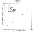
- Fig. 6 shows a plot of the measured FCT gate cathode potential (equivalent to the drain to source potential of the MOSFET) as a function of the applied anode voltage. It can be observed that the drain- source voltage of the MOSFET remains at less than 50 volts for an anode voltage over 600 volts. This feature is extremely important for operation of the circuit because it allows the use of a low breakdown voltage MOSFET device for controlling the load current. These low voltage MOS-FETs can be designed with a low on-resistance, so that power dissipation in the MOSFET in the on condition is low.
- a typical FCT forward voltage drop is about 1.5 volts and a typical MOSFET voltage drop is less than 0.5 volts to obtain an overall forward drop in the circuit of about 2.0 volts.
- the gating circuit shown in Fig. 2 has the additional advantage of achieving forced gate turn-off of the anode current with a very high gate turn-off current gain.
- the switch 50 is used to connect the gate 46 of the MOSFET to ground potential. When this is done, the MOSFET switches from its conducting state to its blocking state. In order to accomplish this, a displacement current must flow to discharge the input capacitance of the MOSFET. Once the MOSFET turns off, its drain potential rises. This produces a reverse bias on the gate junction of the FCT. The minority carriers stored in the n-base of the FCT are then removed via the gate 44 until the FCT 36 becomes reverse biased and starts blocking anode voltage.
- the current flowing out of the gate is equal to the anode current of the FCT until the gate junction begins to support the anode voltage. Any remaining charge will decay by recombination.
- This process is similar to reverse recovery process in a p-i-n rectifier.
- removal of the stored charge in the FCT occurs under conditions similar to unity current gain turn-off for the conventional circuit shown in Fig. 1. As discussed in the introduction, this has been observed to ensure very rapid turn-off of the FCT.
- the gate drive current required during turn-off is determined by the displacement current required for discharging the gate capacitance of the MOSFET.
- a very low gate drive current is used to charge and discharge the MOSFET gate capacitance while turning on and off large anode currents.
- the new gate circuit offers very high gate turn-off current gains at very fast turn-off speeds.
- the current flow through the composite device is obtained by applying a gate voltage at the desired time to turn on the MOSFET. When this current is to be stopped, the gate bias is removed. Consequently, these devices exhibit a large current gain for turn-on and turn-off. Further, in the steady-state bias condition (either on or off state) no gate drive current is needed.
- FIG. 3 An alternative embodiment of the instant invention is shown in Fig. 3.
- a high voltage, normally-on junction field effect transistor 62 is connected to a low voltage MOSFET 64, as shown.
- the operation of the circuit 60 for the JFET 62 is similar to that described above for the FCT.
- the circuit 60 cannot conduct current, because voltage is supported across the gate 66 of the JFET 62.
- the application of a positive voltage to the drain 68 of the JFET reverse biases its gate 66.
- the MOSFET turns on. This short circuits the gate 66 of the JFET to the source 67.
- a further embodiment of the instant invention employs a composite circuit 70 in which a low voltage bipolar transistor 72 is employed to control a high voltage normally-on field controlled thyristor 74 as shown in Fig. 4.
- the collector 78 of the bipolar transistor is connected to the cathode 73 of the field controlled thyristor and emitter 79 of the bipolar transistor is connected to the gate 76 of the field controlled thyristor.
- the on/off state of the combination is controlled by a gate current applied to the gate 71 of the bipolar transistor 72.
- the circuit of Fig. 4 operates as follows: with no gate current applied to the bipolar transistor gate 71, the composite circuit 70 cannot conduct current, because voltage is supported across the gate junction of the FCT 74. If a load voltage is applied, transistor 72 remains in its off state and does not allow current flow between its collector 78 and emitter 79. The breakdown voltage of the transistor 72 should be chosen sufficiently high to avoid avalanche breakdown, as discussed previously.
- the application of the positive voltage to anode 75 of the FCT 74 reverse biases its gate junction, as described above relative to Fig. 2. When a positive voltage is applied to the gate 71 of transistor 72, the transistor 72 turns on. This short circuits the gate 76 of the FCT 74 to the cathode 73.
- FCT 74 The potential barrier between the anode and cathode of FCT 74 is removed and current flow occurs between anode 75 and terminal 77.
- gate 71 of transistor 72 is connected to ground potential, which switches transistor 72 from its conducting to its blocking state, and the collector potential rises. This produces a reverse bias on the gate junction of FCT 74. Minority carriers stored in the n-base of the FCT are then removed via gate 76 until FCT 74 becomes reverse biased and starts blocking anode voltage. Thus, a very low gate drive current is used to turn on and turn off large anode currents.
- the composite circuit 80 comprises a JFET 82 connected in series with a bipolar transistor 84.
- Current control through the composite circuit 80 is obtained by controlling the gate current applied to the bipolar transistor 84.
- no current is applied to gate 83 of transistor 84 no current flows between the collector 86 and emitter 88, the circuit 80 cannot conduct current, because voltage is supported across the gate 81 of JFET 82.
- the application of positive voltage to drain 85 of JFET 82 reverse biases its gate 81.
- the transistor 84 turns on, short-circuiting the gate 81 to source 87 of the JFET 82. Current can now flow from source 87 to drain 85, since the potential barrier has been removed. This source to drain current flows through transistor 84 to terminal 89. Turn-off can be achieved by removal of the gate current as described above.
- a 10 ampere FCT which can operate up to 1,000 volts with a forward voltage drop of 1.5 volts during forward conduction at a current density of 300 amperes per square centimeter and a MOSFET able to carry 50 amps at a forward voltage drop of 0.5 volts and operate at a breakdown voltage of less than 50 volts were connected in series.
- Such an arrangement can be made of a combination of separate FCT and MOSFET devices or as an integrated device as described in U.S. Patent application Serial No. 212,181, filed December 2, 1980.
- the characteristics of the composite FCT MOSFET circuit were measured using a curve tracer and are shown in Fig. 9. These characteristics were obtained by applying gate bias voltages of +5, +3.8, +3.4 and +3.2 volts to obtain the displayed characteristics. At the lower gate voltages, the MOSFET current saturates producing the observed saturation in the composite device characteristics. This can be observed in the MOSFET characteristics shown in Fig. 7 taken with similar gate bias voltages. At larger gate voltages (e.g., +5 volts) the characteristic follows the FCT characteristics obtained with the gate of the FCT shorted to the cathode of the FCT. This characteristic is shown in Fig. 8. Thus, the composite circuit has the expected terminal characteristic.
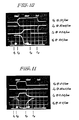
- Gate turn-on and turn-off measurements were also done using the composite circuit shown in Fig. 2. Typical wave forms are as shown in Fig. 10. It can be seen that when the anode voltage is initially applied at time t 1 , no anode current flows until the 5 volt gate bias is applied at time t 2 . The composite structure then allows anode cathode current flow until time t 3 . At time t 3 , the anode voltage is turned off and the current abruptly falls to zero. The gate voltage is turned off at time t 4 . This demonstrates turn-off due to anode voltage being switched off.
- the device can also be turned off by switching off the gate voltage to the MOSFET while anode current is flowing. This is demonstrated in Fig. 11.
- the anode voltage is applied followed by application of the gate bias at time t 2 .
- the anode current begins to flow at time t 2 .
- the gate bias voltage is switched off.
- the MOSFET now turns off.
- the anode current then drops abruptly from 0.5 amps to about 0.25 amps.
- the anode voltage simultaneously rises from about 1.5 volts to about 12 volts.
- the gate of the FCT is reverse biased.
- the remaining stored charge in the base of the FCT then decays by recombination producing a decay in the anode current to zero in about 7 microseconds.
- the anode voltage is turned off later at time t 4 . It is worth pointing out that during both turn-on and turn-off, peak gate currents of less than 0.1 amp are observed for anode currents of up to 2 amperes.
- the gate turn-off gain is thus greater than 20 for the circuit of this invention.
- the instant invention provides the ability to conduct large current with low forward voltage drop, the ability to block large anode voltage when using low voltage MOSFET devices for gating the high voltage device, the ability to turn-on and turn-off anode current with gate bias applied to the MOSFET and high turn-on and turn-off gains.
Description
- This invention relates to a circuit for controlling the conducting state of a high-voltage normally-on semiconductor device according to the precharacterizing part of
claim 1. Such system is known from DE-A-2 906 961. - Prior art field controlled thyristors have been developed for power switching applications. These devices can block current flow for both polarities of applied anode voltage, and can also conduct forward current with a low forward voltage drop. These devices have also been shown to exhibit gate turn-off capability with turn-off times of less than 1 microsecond. To obtain forward blocking characteristics in this device, it is necessary to apply a negative bias to the gate. This negative bias reverse biases the gate junction and causes a depletion layer to extend under the cathode. When the depletion layers of adjacent gate regions punch through under the cathode, a potential barrier is formed between the anode and the cathode. This potential barrier prevents the injection of electrons from the cathode to the anode and, thus, allows the device to block the current flow. However, as the anode voltage increases, the potential barrier height decreases. When the anode voltage is increased beyond a cetain value for each applied gate bias voltage, anode current flow will commence. The ratio of the anode voltage to the applied gate bias is defined as a blocking gain of the device. Thus, the field controlled thyristor has a normally-on characteristic and requires the application of a gate voltage to maintain it in the off state.
- Field controlled thyristors can be switched rapidly from the conducting mode to the forward blocking mode by the application of a negative gate voltage while the anode current is flowing. During gate turn-off, sufficient gate current must be supplied by the gate drive circuit so 'as to remove the minority carrier stored charge in the n-base and to allow the gate depletion layer to extend under the cathode to pinch off the anode -current flow. It has been found that turn-off times of less than 1 microsecond can be achieved when the peak gate turn-off current is comparable to the anode current.
- A conventional prior art circuit used for gating field controlled thyristors (FCT) is shown in Fig. 1. In
circuit 10, current supply to theload 12 by the power supply 14 can be controlled by gating the field controlledthyristor 16 using aswitch 18. Whenswitch 18 is open, FCT 16 is in its on state and the current is supplied to theload 12. When theswtich 18 is closed, the gate voltage supplied by a source, shown schematically by 20 and 22, is used to maintain the FCT in its forward blocking mode. The turn-off speed of the FCT is controlled by the peak gate current during turn-off. This current can be controlled by thegate resistance 22. Several problems have been encountered with the use of this gating circuit. First, the devices are normally-on in the absence of a gate bias voltage, and the circuits cannot ensure fail- safe start-up and operation. Second, the devices require a substantial gate voltage in order to operate them at large forward blocking voltages. This problem has been partially overcome in the prior art by improvements in the device structure, which have allowed the development of devices with high blocking gains. In spite of improvements of blocking gain, some gate bias voltage is necessary to maintain these devices in their forward blocking mode. Third, these devices require substantial gate drive currents to switch them from the on state to the blocking state. Thus, although turn-off times of a few microseconds have been observed, gate turn-off current gains of less than 5 are typically necessary to achieve these high turn-off speeds. These drawbacks of the field controlled thyristors have been primarily responsible for its limited application to power switching applications. - An object of the instant invention is to provide a circuit configuration including a high breakdown voltage normally-on power device connected in series with a low breakdown voltage normally-off power device such that the circuit can be operated in a normally-off mode; the turn-on and turn-off of the circuit is controlled by controlling the low voltage power device. It is a second object of the instant invention to provide a high voltage normally-off device configuration which exhibits fast gate turn-off with a very high gate turn-off gain.
- Accordingly, the instant invention as claimed describes a composite circuit including a high voltage normally-on device connected in series with a low voltage, normally-off transistor such that the low voltage, normally-off transistor controls current flow through the composite circuit. In one embodiment, the instant invention includes a field controlled thyristor having in series with the cathode thereof a low voltage MOSFET. An alternative preferred embodiment includes a junction field effect transistor, JFET, having a low voltage MOSFET connected in series with the source of the JFET. In further preferred embodiments, a low voltage bipolar transistor is connected in series with the cathode of a high voltage field controlled thyristor or the source of a high voltage JFET.
- The features of the invention believed to be novel and unobvious over the prior art are set forth with particularity in the appended claims. The invention itself, including organization and method of operation, may best be understood by reference to the following description taken in conjunction with the accompanying drawings in which:
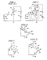
- Fig. 1 is a schematic circuit diagram showing a prior art technique for controlling a high voltage field controlled thyristor;
- Fig. 2 is a schematic circuit diagram showing one preferred embodiment of the instant invention;
- Fig. 3 is a schematic circuit diagram illustrating an alternative preferred embodiment of the instant invention;
- Fig. 4 is a schematic circuit diagram illustrating another preferred embodiment of the instant invention;
- Fig. 5 is a schematic circuit diagram illustrating yet another preferred embodiment of the instant invention;
- Fig. 6 is a graph schematically illustrating a characteristic of the embodiment of Fig. 2;
- Fig. 7 illustrates the characteristics of a MOSFET;
- Fig. 8 illustrates typical characteristics of a field controlled thyristor;
- Fig. 9 illustrates the characteristics of the composite circuit illustrated in Fig. 2; and
- Figs. 10 and 11 illustrate switching characteristics of a composite AFCT and MOSFET circuit.
- The problems discussed above in the conventional gating technique for field controlled thyristors can be solved by using the new gating circuits discussed herein. In each of the embodiments described herein, a high voltage normally-on device is caused to operate in a normally-off mode by adding a low voltage normally-off device in series with the high voltage device. A gating circuit 30 employing our instant invention is shown in Fig. 2. In the
composite circuit 32, an n channel, normally-off, MOS gated field effect transistor 34 is used to control the current flow through the normally-on field controlled thyristor 36. As used herein, "normally-on" means a device which conducts current in the absence of gate bias and requires a gate bias to block current flow. As used herein, "normally-off" means a device which blocks current in the absence of gate bias and conducts current when gate bias is applied. As used herein, "high voltage" is a voltage of 100 volts or greater and "low voltage" is a voltage less than 100 volts. To accomplish this, the drain 38 of the MOSFET 34 is connected to the cathode 40 .of the FCT 36 and the source 42 of the MOSFET is connected to the gate 44 of the FCT. The current conduction through theload 12 is then controlled by the bias applied to thegate 46 of the MOSFET 34. - The circuit in Fig. 2 operates as follows: with no gate bias applied to the MOSFET, the
composite circuit 32 cannot conduct current, because voltage is supported across the gate junction of the FCT. If the load voltage VL is applied, the MOSFET 34 remains in its off state and does not allow current flow between its drain 38 and source 42 terminals. The breakdown voltage of the MOSFET should be sufficiently high to avoid avalanche breakdown, as described hereinafter. The application of the positive voltage to the anode 48 of the FCT reverse biases its gate junction. The depletion layer of the gate junction then spreads under the cathode of the FCT and establishes a potential barrier between the anode and the cathode. This process shields the cathode potential from the anode potential. When a positive voltage is applied to theMOSFET gate 46 with respect to the cathode which is at ground potential, the MOSFET turns on. This short-circuits the gate 44 of the FCT to the cathode 40. This now allows current flow from the anode to the cathode, since the potential barrier is removed. This current flows through the MOSFET 34 to the cathode terminal 40. In order to deliver current to the load, the switch 50 is used to connect thegate 46 to the positivegate power supply 20. This positive gate bias must exceed the threshold voltage of the MOSFET 34 in order to switch it to the conducting state. When the MOSFET is in its conducting state, the load current can now flow through the FCT from the anode to the cathode and via the drain of the MOSFET to the ground terminal. Thus, as mentioned earlier, in this circuit the full load current flows through the MOSFET. - The operating characteristics of the circuit 30 are schematically illustrated in Fig. 6, which shows a plot of the measured FCT gate cathode potential (equivalent to the drain to source potential of the MOSFET) as a function of the applied anode voltage. It can be observed that the drain- source voltage of the MOSFET remains at less than 50 volts for an anode voltage over 600 volts. This feature is extremely important for operation of the circuit because it allows the use of a low breakdown voltage MOSFET device for controlling the load current. These low voltage MOS-FETs can be designed with a low on-resistance, so that power dissipation in the MOSFET in the on condition is low. Thus, although the full FCT current must pass through the MOSFET when it is turned on, the voltage across the MOSFET is small, so that a low breakdown voltage MOSFET can be used here. A typical FCT forward voltage drop is about 1.5 volts and a typical MOSFET voltage drop is less than 0.5 volts to obtain an overall forward drop in the circuit of about 2.0 volts.
- The gating circuit shown in Fig. 2 has the additional advantage of achieving forced gate turn-off of the anode current with a very high gate turn-off current gain. In order to turn off the load current, the switch 50 is used to connect the
gate 46 of the MOSFET to ground potential. When this is done, the MOSFET switches from its conducting state to its blocking state. In order to accomplish this, a displacement current must flow to discharge the input capacitance of the MOSFET. Once the MOSFET turns off, its drain potential rises. This produces a reverse bias on the gate junction of the FCT. The minority carriers stored in the n-base of the FCT are then removed via the gate 44 until the FCT 36 becomes reverse biased and starts blocking anode voltage. The current flowing out of the gate is equal to the anode current of the FCT until the gate junction begins to support the anode voltage. Any remaining charge will decay by recombination. This process is similar to reverse recovery process in a p-i-n rectifier. Thus, removal of the stored charge in the FCT occurs under conditions similar to unity current gain turn-off for the conventional circuit shown in Fig. 1. As discussed in the introduction, this has been observed to ensure very rapid turn-off of the FCT. However, in the new gating circuit shown in Fig. 2, the gate drive current required during turn-off is determined by the displacement current required for discharging the gate capacitance of the MOSFET. Thus, in this gating scheme, a very low gate drive current is used to charge and discharge the MOSFET gate capacitance while turning on and off large anode currents. Thus, the new gate circuit offers very high gate turn-off current gains at very fast turn-off speeds. In dynamic circuit operation, the current flow through the composite device is obtained by applying a gate voltage at the desired time to turn on the MOSFET. When this current is to be stopped, the gate bias is removed. Consequently, these devices exhibit a large current gain for turn-on and turn-off. Further, in the steady-state bias condition (either on or off state) no gate drive current is needed. - An alternative embodiment of the instant invention is shown in Fig. 3. In this embodiment, a high voltage, normally-on junction
field effect transistor 62 is connected to alow voltage MOSFET 64, as shown. The operation of the circuit 60 for theJFET 62 is similar to that described above for the FCT. When no gate bias is applied to theMOSFET 64, the circuit 60 cannot conduct current, because voltage is supported across thegate 66 of theJFET 62. The application of a positive voltage to the drain 68 of the JFET reverse biases itsgate 66. When a positive voltage is applied to the MOSFET gate 65 with respect to thesource 69, the MOSFET turns on. This short circuits thegate 66 of the JFET to the source 67. This allows current flow from the source 67 to the drain 68, since the potential barrier has been removed. This source- to-drain current flows through theMOSFET 64 to thesource terminal 69. When gate bias is removed from the MOSFET, the device current is blocked, as described above relative to Fig. 2. - A further embodiment of the instant invention employs a
composite circuit 70 in which a low voltagebipolar transistor 72 is employed to control a high voltage normally-on field controlled thyristor 74 as shown in Fig. 4. In this configuration, thecollector 78 of the bipolar transistor is connected to the cathode 73 of the field controlled thyristor andemitter 79 of the bipolar transistor is connected to thegate 76 of the field controlled thyristor. The on/off state of the combination is controlled by a gate current applied to the gate 71 of thebipolar transistor 72. - The circuit of Fig. 4 operates as follows: with no gate current applied to the bipolar transistor gate 71, the
composite circuit 70 cannot conduct current, because voltage is supported across the gate junction of the FCT 74. If a load voltage is applied,transistor 72 remains in its off state and does not allow current flow between itscollector 78 andemitter 79. The breakdown voltage of thetransistor 72 should be chosen sufficiently high to avoid avalanche breakdown, as discussed previously. The application of the positive voltage to anode 75 of the FCT 74 reverse biases its gate junction, as described above relative to Fig. 2. When a positive voltage is applied to the gate 71 oftransistor 72, thetransistor 72 turns on. This short circuits thegate 76 of the FCT 74 to the cathode 73. The potential barrier between the anode and cathode of FCT 74 is removed and current flow occurs betweenanode 75 and terminal 77. In order to turn off thecomposite circuit 70, gate 71 oftransistor 72 is connected to ground potential, which switchestransistor 72 from its conducting to its blocking state, and the collector potential rises. This produces a reverse bias on the gate junction of FCT 74. Minority carriers stored in the n-base of the FCT are then removed viagate 76 until FCT 74 becomes reverse biased and starts blocking anode voltage. Thus, a very low gate drive current is used to turn on and turn off large anode currents. - Yet another embodiment of the instant invention is shown in Fig. 5, in which the
composite circuit 80 comprises aJFET 82 connected in series with abipolar transistor 84. Current control through thecomposite circuit 80 is obtained by controlling the gate current applied to thebipolar transistor 84. When no current is applied togate 83 oftransistor 84 no current flows between the collector 86 andemitter 88, thecircuit 80 cannot conduct current, because voltage is supported across the gate 81 ofJFET 82. The application of positive voltage to drain 85 ofJFET 82 reverse biases its gate 81. When current is applied togate 83 oftransistor 84, thetransistor 84 turns on, short-circuiting the gate 81 to source 87 of theJFET 82. Current can now flow from source 87 to drain 85, since the potential barrier has been removed. This source to drain current flows throughtransistor 84 to terminal 89. Turn-off can be achieved by removal of the gate current as described above. - As a specific example, a 10 ampere FCT, which can operate up to 1,000 volts with a forward voltage drop of 1.5 volts during forward conduction at a current density of 300 amperes per square centimeter and a MOSFET able to carry 50 amps at a forward voltage drop of 0.5 volts and operate at a breakdown voltage of less than 50 volts were connected in series. Such an arrangement can be made of a combination of separate FCT and MOSFET devices or as an integrated device as described in U.S. Patent application Serial No. 212,181, filed December 2, 1980.
- The characteristics of the composite FCT MOSFET circuit were measured using a curve tracer and are shown in Fig. 9. These characteristics were obtained by applying gate bias voltages of +5, +3.8, +3.4 and +3.2 volts to obtain the displayed characteristics. At the lower gate voltages, the MOSFET current saturates producing the observed saturation in the composite device characteristics. This can be observed in the MOSFET characteristics shown in Fig. 7 taken with similar gate bias voltages. At larger gate voltages (e.g., +5 volts) the characteristic follows the FCT characteristics obtained with the gate of the FCT shorted to the cathode of the FCT. This characteristic is shown in Fig. 8. Thus, the composite circuit has the expected terminal characteristic.
- Gate turn-on and turn-off measurements were also done using the composite circuit shown in Fig. 2. Typical wave forms are as shown in Fig. 10. It can be seen that when the anode voltage is initially applied at time t1, no anode current flows until the 5 volt gate bias is applied at time t2. The composite structure then allows anode cathode current flow until time t3. At time t3, the anode voltage is turned off and the current abruptly falls to zero. The gate voltage is turned off at time t4. This demonstrates turn-off due to anode voltage being switched off.
- The device can also be turned off by switching off the gate voltage to the MOSFET while anode current is flowing. This is demonstrated in Fig. 11. At time t,, the anode voltage is applied followed by application of the gate bias at time t2. The anode current begins to flow at time t2. At time t3, the gate bias voltage is switched off. The MOSFET now turns off. The anode current then drops abruptly from 0.5 amps to about 0.25 amps. The anode voltage simultaneously rises from about 1.5 volts to about 12 volts. At this point, the gate of the FCT is reverse biased. The remaining stored charge in the base of the FCT then decays by recombination producing a decay in the anode current to zero in about 7 microseconds. The anode voltage is turned off later at time t4. It is worth pointing out that during both turn-on and turn-off, peak gate currents of less than 0.1 amp are observed for anode currents of up to 2 amperes. The gate turn-off gain is thus greater than 20 for the circuit of this invention.
- As shown above, the instant invention provides the ability to conduct large current with low forward voltage drop, the ability to block large anode voltage when using low voltage MOSFET devices for gating the high voltage device, the ability to turn-on and turn-off anode current with gate bias applied to the MOSFET and high turn-on and turn-off gains.
Claims (5)
Applications Claiming Priority (2)
| Application Number | Priority Date | Filing Date | Title |
|---|---|---|---|
| US257080 | 1981-04-24 | ||
| US06/257,080 US4663547A (en) | 1981-04-24 | 1981-04-24 | Composite circuit for power semiconductor switching |
Publications (3)
| Publication Number | Publication Date |
|---|---|
| EP0063749A2 EP0063749A2 (en) | 1982-11-03 |
| EP0063749A3 EP0063749A3 (en) | 1983-03-16 |
| EP0063749B1 true EP0063749B1 (en) | 1986-02-05 |
Family
ID=22974791
Family Applications (1)
| Application Number | Title | Priority Date | Filing Date |
|---|---|---|---|
| EP82103158A Expired EP0063749B1 (en) | 1981-04-24 | 1982-04-15 | Composite circuit for power semiconductor switching |
Country Status (6)
| Country | Link |
|---|---|
| US (1) | US4663547A (en) |
| EP (1) | EP0063749B1 (en) |
| JP (1) | JPS57193124A (en) |
| DE (1) | DE3268921D1 (en) |
| IE (1) | IE52585B1 (en) |
| MX (1) | MX151073A (en) |
Cited By (2)
| Publication number | Priority date | Publication date | Assignee | Title |
|---|---|---|---|---|
| DE10135835C1 (en) * | 2001-07-23 | 2002-08-22 | Siced Elect Dev Gmbh & Co Kg | Switching device for switching at a high operating voltage |
| DE102010027832B3 (en) * | 2010-04-15 | 2011-07-28 | Infineon Technologies AG, 85579 | Semiconductor switching arrangement, has drive circuit switched between control terminal and load track terminals of semiconductor component, where track terminals are arranged between component and another component |
Families Citing this family (60)
| Publication number | Priority date | Publication date | Assignee | Title |
|---|---|---|---|---|
| US4523111A (en) * | 1983-03-07 | 1985-06-11 | General Electric Company | Normally-off, gate-controlled electrical circuit with low on-resistance |
| DE3331015A1 (en) * | 1983-08-27 | 1985-03-14 | ANT Nachrichtentechnik GmbH, 7150 Backnang | Circuit arrangement for the DC isolation of two voltages |
| DE3481107D1 (en) * | 1983-10-14 | 1990-02-22 | Omron Tateisi Electronics Co | ELECTRONIC CIRCUIT ARRANGEMENT. |
| EP0157937B1 (en) * | 1984-04-11 | 1987-09-02 | Siemens Aktiengesellschaft | Electronic switch |
| DE3427498C2 (en) * | 1984-07-26 | 1986-08-07 | Ifm Electronic Gmbh, 4300 Essen | Electronic, preferably non-contact switching device |
| DE3586735D1 (en) * | 1984-10-19 | 1992-11-12 | Bbc Brown Boveri & Cie | DISABLED POWER SEMICONDUCTOR COMPONENT. |
| NL8501816A (en) * | 1985-06-24 | 1987-01-16 | Johan Dirk Spek | ELECTRONIC CHAIN COMPONENT WITH FIELD-EFFECT TRANSISTOR OPERATION, APPLICATIONS OF THIS CHAIN COMPONENT, AND REPLACEMENT CHAIN FOR SUCH A COMPONENT. |
| CH668667A5 (en) * | 1985-11-15 | 1989-01-13 | Bbc Brown Boveri & Cie | PERFORMANCE SEMICONDUCTOR MODULE. |
| JPH0760997B2 (en) * | 1986-06-09 | 1995-06-28 | 日本テキサス・インスツルメンツ株式会社 | High voltage output circuit |
| US4945266A (en) * | 1987-11-18 | 1990-07-31 | Mitsubishi Denki Kabushiki Kaisha | Composite semiconductor device |
| JPH01133413A (en) * | 1987-11-18 | 1989-05-25 | Mitsubishi Electric Corp | Composite semiconductor device |
| IT1224644B (en) * | 1987-12-22 | 1990-10-18 | Sgs Thomson Microelectronics | CIRCUIT FOR MAINTAINING A MOS TRANSISTOR IN CONDUCT WITHOUT POWER SUPPLY VOLTAGE. |
| FR2627033B1 (en) * | 1988-02-04 | 1990-07-20 | Sgs Thomson Microelectronics | GRID CONTROL CIRCUIT OF A SWITCHING POWER MOS TRANSISTOR |
| DE58905844D1 (en) * | 1989-02-02 | 1993-11-11 | Asea Brown Boveri | Pressure-contacted semiconductor device. |
| JPH0810823B2 (en) * | 1990-10-12 | 1996-01-31 | 東洋電機製造株式会社 | Composite semiconductor device |
| NL9101044A (en) * | 1991-06-17 | 1993-01-18 | Sierra Semiconductor Bv | AC VOLTAGE LIMITER IN MOS TECHNOLOGY. |
| JPH0575110A (en) * | 1991-09-13 | 1993-03-26 | Fuji Electric Co Ltd | Semiconductor device |
| JPH05110407A (en) * | 1991-10-14 | 1993-04-30 | Sony Corp | Thyristor trigger circuit |
| US5319222A (en) * | 1992-04-29 | 1994-06-07 | North Carolina State University | MOS gated thyristor having on-state current saturation capability |
| US5317171A (en) * | 1992-04-29 | 1994-05-31 | North Carolina State University | MOS gated thyristor with remote turn-off electrode |
| US6127746A (en) * | 1996-10-21 | 2000-10-03 | International Rectifier Corp. | Method of controlling the switching DI/DT and DV/DT of a MOS-gated power transistor |
| WO2000077933A1 (en) * | 1999-06-11 | 2000-12-21 | Siemens Aktiengesellschaft | Circuit comprising a disconnectable power semiconductor switch |
| US7820511B2 (en) | 2004-07-08 | 2010-10-26 | Semisouth Laboratories, Inc. | Normally-off integrated JFET power switches in wide bandgap semiconductors and methods of making |
| US7202528B2 (en) * | 2004-12-01 | 2007-04-10 | Semisouth Laboratories, Inc. | Normally-off integrated JFET power switches in wide bandgap semiconductors and methods of making |
| US7119380B2 (en) * | 2004-12-01 | 2006-10-10 | Semisouth Laboratories, Inc. | Lateral trench field-effect transistors in wide bandgap semiconductor materials, methods of making, and integrated circuits incorporating the transistors |
| US7602157B2 (en) * | 2005-12-28 | 2009-10-13 | Flyback Energy, Inc. | Supply architecture for inductive loads |
| US7888768B2 (en) * | 2006-01-09 | 2011-02-15 | Fairchild Korea Semiconductor, Ltd. | Power integrated circuit device having embedded high-side power switch |
| DE102006029928B3 (en) * | 2006-06-29 | 2007-09-06 | Siemens Ag | Electronic switching device for switching high electric current, has isolating unit connected between control connection of switching unit and load supply of another switching unit, where isolation unit decouples switching units |
| CN101919150B (en) * | 2007-09-18 | 2013-12-18 | 菲莱贝克能源公司 | Current waveform construction to generate AC power with low harmonic distortion from localized energy sources |
| SE533026C2 (en) * | 2008-04-04 | 2010-06-08 | Klas-Haakan Eklund | Field effect transistor with isolated gate connected in series with a JFET |
| US7777553B2 (en) * | 2008-04-08 | 2010-08-17 | Infineon Technologies Austria Ag | Simplified switching circuit |
| US7825467B2 (en) * | 2008-09-30 | 2010-11-02 | Infineon Technologies Austria Ag | Semiconductor component having a drift zone and a drift control zone |
| US8294507B2 (en) * | 2009-05-08 | 2012-10-23 | Cree, Inc. | Wide bandgap bipolar turn-off thyristor having non-negative temperature coefficient and related control circuits |
| US8860273B2 (en) * | 2009-12-28 | 2014-10-14 | Flyback Energy, Inc. | External field interaction motor |
| CA2785715A1 (en) * | 2009-12-28 | 2011-07-28 | Paul M. Babcock | Controllable universal supply with reactive power management |
| WO2011100304A1 (en) | 2010-02-09 | 2011-08-18 | Massachusetts Institute Of Technology | Dual-gate normally-off nitride transistors |
| WO2011108501A1 (en) * | 2010-03-02 | 2011-09-09 | 本田技研工業株式会社 | Load driving device |
| US8310281B2 (en) | 2010-11-30 | 2012-11-13 | Infineon Technologies Ag | System and method for driving a cascode switch |
| US8558584B2 (en) | 2010-11-30 | 2013-10-15 | Infineon Technologies Ag | System and method for bootstrapping a switch driver |
| US8487664B2 (en) | 2010-11-30 | 2013-07-16 | Infineon Technologies Ag | System and method for driving a switch |
| US8896131B2 (en) | 2011-02-03 | 2014-11-25 | Alpha And Omega Semiconductor Incorporated | Cascode scheme for improved device switching behavior |
| US9859882B2 (en) | 2011-03-21 | 2018-01-02 | Infineon Technologies Americas Corp. | High voltage composite semiconductor device with protection for a low voltage device |
| US9362905B2 (en) | 2011-03-21 | 2016-06-07 | Infineon Technologies Americas Corp. | Composite semiconductor device with turn-on prevention control |
| US8766375B2 (en) | 2011-03-21 | 2014-07-01 | International Rectifier Corporation | Composite semiconductor device with active oscillation prevention |
| US8536931B2 (en) | 2011-06-17 | 2013-09-17 | Rf Micro Devices, Inc. | BI-FET cascode power switch |
| TW201340078A (en) * | 2012-03-22 | 2013-10-01 | Richtek Technology Corp | Voltage conversion circuit and method for improving efficiency of a driver |
| JP5979998B2 (en) | 2012-06-18 | 2016-08-31 | ルネサスエレクトロニクス株式会社 | Semiconductor device and system using the same |
| ITTO20121081A1 (en) | 2012-12-14 | 2014-06-15 | St Microelectronics Srl | ELECTRONIC POWER COMPONENT NORMALLY OFF |
| DE102012112391B4 (en) | 2012-12-17 | 2018-10-04 | Phoenix Contact Gmbh & Co. Kg | Switching power supply with a cascode circuit |
| US9007117B2 (en) * | 2013-08-02 | 2015-04-14 | Infineon Technologies Dresden Gmbh | Solid-state switching device having a high-voltage switching transistor and a low-voltage driver transistor |
| US9331068B2 (en) | 2013-10-30 | 2016-05-03 | United Silicon Carbide, Inc. | Hybrid wide-bandgap semiconductor bipolar switches |
| US9148139B2 (en) | 2014-01-13 | 2015-09-29 | United Silicon Carbide, Inc. | Monolithically integrated cascode switches |
| US9083343B1 (en) | 2014-05-28 | 2015-07-14 | United Silicon Carbide, Inc. | Cascode switching circuit |
| CN106300929B (en) * | 2015-05-21 | 2019-03-15 | 台达电子工业股份有限公司 | Switching circuit |
| JP6646363B2 (en) | 2015-06-02 | 2020-02-14 | 株式会社アドバンテスト | Semiconductor device |
| US9871510B1 (en) | 2016-08-24 | 2018-01-16 | Power Integrations, Inc. | Clamp for a hybrid switch |
| JP6769458B2 (en) | 2017-07-26 | 2020-10-14 | 株式会社デンソー | Semiconductor device |
| US11144493B1 (en) | 2018-05-02 | 2021-10-12 | Ecosense Lighting Inc. | Composite interface circuit |
| JP7024688B2 (en) | 2018-11-07 | 2022-02-24 | 株式会社デンソー | Semiconductor device |
| CN111555742A (en) * | 2020-05-07 | 2020-08-18 | 漳州科华技术有限责任公司 | Combination switch element and uninterrupted power source |
Family Cites Families (6)
| Publication number | Priority date | Publication date | Assignee | Title |
|---|---|---|---|---|
| US3268776A (en) * | 1962-11-21 | 1966-08-23 | Western Electric Co | Driver for pulsing inductive loads |
| US3614474A (en) * | 1968-10-24 | 1971-10-19 | Texas Instruments Inc | Semiconductor power-switching apparatus |
| US3916222A (en) * | 1974-05-28 | 1975-10-28 | Nat Semiconductor Corp | Field effect transistor switching circuit |
| US4107725A (en) * | 1974-08-02 | 1978-08-15 | Nippon Gakki Seizo Kabushiki Kaisha | Compound field effect transistor |
| JPS5233464A (en) * | 1975-09-10 | 1977-03-14 | Toshiba Corp | Logic circuit |
| JPS54112157A (en) * | 1978-02-23 | 1979-09-01 | Hitachi Ltd | Control circuit for field effect thyristor |
-
1981
- 1981-04-24 US US06/257,080 patent/US4663547A/en not_active Expired - Lifetime
-
1982
- 1982-04-06 IE IE818/82A patent/IE52585B1/en not_active IP Right Cessation
- 1982-04-15 EP EP82103158A patent/EP0063749B1/en not_active Expired
- 1982-04-15 DE DE8282103158T patent/DE3268921D1/en not_active Expired
- 1982-04-21 JP JP57065569A patent/JPS57193124A/en active Granted
- 1982-04-23 MX MX192410A patent/MX151073A/en unknown
Cited By (3)
| Publication number | Priority date | Publication date | Assignee | Title |
|---|---|---|---|---|
| DE10135835C1 (en) * | 2001-07-23 | 2002-08-22 | Siced Elect Dev Gmbh & Co Kg | Switching device for switching at a high operating voltage |
| US6822842B2 (en) | 2001-07-23 | 2004-11-23 | Siced Electronics Development Gmbh & Co. Kg | Switching device for switching at a high operating voltage |
| DE102010027832B3 (en) * | 2010-04-15 | 2011-07-28 | Infineon Technologies AG, 85579 | Semiconductor switching arrangement, has drive circuit switched between control terminal and load track terminals of semiconductor component, where track terminals are arranged between component and another component |
Also Published As
| Publication number | Publication date |
|---|---|
| EP0063749A3 (en) | 1983-03-16 |
| IE820818L (en) | 1982-10-24 |
| MX151073A (en) | 1984-09-20 |
| US4663547A (en) | 1987-05-05 |
| JPH0434330B2 (en) | 1992-06-05 |
| IE52585B1 (en) | 1987-12-23 |
| JPS57193124A (en) | 1982-11-27 |
| DE3268921D1 (en) | 1986-03-20 |
| EP0063749A2 (en) | 1982-11-03 |
Similar Documents
| Publication | Publication Date | Title |
|---|---|---|
| EP0063749B1 (en) | Composite circuit for power semiconductor switching | |
| US5413313A (en) | Integrated power switch structure having a vertical thyristor controlled by a lateral MOS transistor | |
| US6933541B1 (en) | Emitter turn-off thyristors (ETO) | |
| US4866315A (en) | Turn-on/off driving technique for insulated gate thyristor | |
| EP0181148A1 (en) | Semiconductor device | |
| DE4318205C2 (en) | Semiconductor devices | |
| US5294816A (en) | Unit cell arrangement for emitter switched thyristor with base resistance control | |
| Sin et al. | Lateral insulated-gate bipolar transistor (LIGBT) with a segmented anode structure | |
| DE112019001054T5 (en) | SEMICONDUCTOR DEVICE AND POWER CONVERSION DEVICE | |
| JPH07169868A (en) | Circuit pattern having at least one bipolar power device | |
| DE19638769C1 (en) | Emitter controlled thyristor | |
| US5659185A (en) | Insulated Gate thyristor | |
| US5621229A (en) | Semiconductor device and control method | |
| US5625203A (en) | Controlled turn-off power semiconductor device | |
| GB2053606A (en) | Improvements in and relating to semiconductor switching circuits | |
| US3927332A (en) | Drive circuit for controlling conduction of a semiconductor device | |
| Seki et al. | Dual gate MOS thyristor (DGMOT) | |
| Baliga | High gain power switching using field controlled thyristors | |
| US4177479A (en) | Electrical circuit with a high-frequency thyristor fired by blocking leakage current | |
| DE10007416C1 (en) | Controlled semiconductor arrangement e.g. for buck-boost circuit or inverters | |
| Kajiwara et al. | High speed high voltage static induction thyristor | |
| KR950008424B1 (en) | Semiconductor switching circuit | |
| WO1999017374A1 (en) | Emitter turn-off thyristors (eto) | |
| KR940008259B1 (en) | Semiconductor device and manufacturing method thereof | |
| GB2130028A (en) | Integrated semiconductor device |
Legal Events
| Date | Code | Title | Description |
|---|---|---|---|
| PUAI | Public reference made under article 153(3) epc to a published international application that has entered the european phase |
Free format text: ORIGINAL CODE: 0009012 |
|
| AK | Designated contracting states |
Designated state(s): CH DE FR GB SE |
|
| PUAL | Search report despatched |
Free format text: ORIGINAL CODE: 0009013 |
|
| AK | Designated contracting states |
Designated state(s): CH DE FR GB LI SE |
|
| 17P | Request for examination filed |
Effective date: 19830827 |
|
| GRAA | (expected) grant |
Free format text: ORIGINAL CODE: 0009210 |
|
| AK | Designated contracting states |
Designated state(s): CH DE FR GB LI SE |
|
| REF | Corresponds to: |
Ref document number: 3268921 Country of ref document: DE Date of ref document: 19860320 |
|
| ET | Fr: translation filed | ||
| PLBE | No opposition filed within time limit |
Free format text: ORIGINAL CODE: 0009261 |
|
| STAA | Information on the status of an ep patent application or granted ep patent |
Free format text: STATUS: NO OPPOSITION FILED WITHIN TIME LIMIT |
|
| 26N | No opposition filed | ||
| EAL | Se: european patent in force in sweden |
Ref document number: 82103158.0 |
|
| PGFP | Annual fee paid to national office [announced via postgrant information from national office to epo] |
Ref country code: FR Payment date: 19960318 Year of fee payment: 15 |
|
| PGFP | Annual fee paid to national office [announced via postgrant information from national office to epo] |
Ref country code: SE Payment date: 19960319 Year of fee payment: 15 |
|
| PGFP | Annual fee paid to national office [announced via postgrant information from national office to epo] |
Ref country code: GB Payment date: 19960322 Year of fee payment: 15 |
|
| PGFP | Annual fee paid to national office [announced via postgrant information from national office to epo] |
Ref country code: DE Payment date: 19960326 Year of fee payment: 15 Ref country code: CH Payment date: 19960326 Year of fee payment: 15 |
|
| PG25 | Lapsed in a contracting state [announced via postgrant information from national office to epo] |
Ref country code: GB Effective date: 19970415 |
|
| PG25 | Lapsed in a contracting state [announced via postgrant information from national office to epo] |
Ref country code: SE Effective date: 19970416 |
|
| PG25 | Lapsed in a contracting state [announced via postgrant information from national office to epo] |
Ref country code: LI Free format text: LAPSE BECAUSE OF NON-PAYMENT OF DUE FEES Effective date: 19970430 Ref country code: CH Free format text: LAPSE BECAUSE OF NON-PAYMENT OF DUE FEES Effective date: 19970430 |
|
| GBPC | Gb: european patent ceased through non-payment of renewal fee |
Effective date: 19970415 |
|
| REG | Reference to a national code |
Ref country code: CH Ref legal event code: PL |
|
| PG25 | Lapsed in a contracting state [announced via postgrant information from national office to epo] |
Ref country code: FR Free format text: LAPSE BECAUSE OF NON-PAYMENT OF DUE FEES Effective date: 19971231 |
|
| PG25 | Lapsed in a contracting state [announced via postgrant information from national office to epo] |
Ref country code: DE Free format text: LAPSE BECAUSE OF NON-PAYMENT OF DUE FEES Effective date: 19980101 |
|
| EUG | Se: european patent has lapsed |
Ref document number: 82103158.0 |
|
| REG | Reference to a national code |
Ref country code: FR Ref legal event code: ST |