EP0068991A2 - Data buffer - Google Patents
Data buffer Download PDFInfo
- Publication number
- EP0068991A2 EP0068991A2 EP82401113A EP82401113A EP0068991A2 EP 0068991 A2 EP0068991 A2 EP 0068991A2 EP 82401113 A EP82401113 A EP 82401113A EP 82401113 A EP82401113 A EP 82401113A EP 0068991 A2 EP0068991 A2 EP 0068991A2
- Authority
- EP
- European Patent Office
- Prior art keywords
- lines
- halt
- computer
- signal
- line
- Prior art date
- Legal status (The legal status is an assumption and is not a legal conclusion. Google has not performed a legal analysis and makes no representation as to the accuracy of the status listed.)
- Withdrawn
Links
Images


Classifications
-
- G—PHYSICS
- G06—COMPUTING; CALCULATING OR COUNTING
- G06F—ELECTRIC DIGITAL DATA PROCESSING
- G06F11/00—Error detection; Error correction; Monitoring
- G06F11/22—Detection or location of defective computer hardware by testing during standby operation or during idle time, e.g. start-up testing
-
- G—PHYSICS
- G01—MEASURING; TESTING
- G01R—MEASURING ELECTRIC VARIABLES; MEASURING MAGNETIC VARIABLES
- G01R31/00—Arrangements for testing electric properties; Arrangements for locating electric faults; Arrangements for electrical testing characterised by what is being tested not provided for elsewhere
- G01R31/28—Testing of electronic circuits, e.g. by signal tracer
- G01R31/2832—Specific tests of electronic circuits not provided for elsewhere
- G01R31/2834—Automated test systems [ATE]; using microprocessors or computers
-
- G—PHYSICS
- G06—COMPUTING; CALCULATING OR COUNTING
- G06F—ELECTRIC DIGITAL DATA PROCESSING
- G06F13/00—Interconnection of, or transfer of information or other signals between, memories, input/output devices or central processing units
- G06F13/38—Information transfer, e.g. on bus
- G06F13/42—Bus transfer protocol, e.g. handshake; Synchronisation
- G06F13/4204—Bus transfer protocol, e.g. handshake; Synchronisation on a parallel bus
- G06F13/4221—Bus transfer protocol, e.g. handshake; Synchronisation on a parallel bus being an input/output bus, e.g. ISA bus, EISA bus, PCI bus, SCSI bus
- G06F13/4226—Bus transfer protocol, e.g. handshake; Synchronisation on a parallel bus being an input/output bus, e.g. ISA bus, EISA bus, PCI bus, SCSI bus with asynchronous protocol
-
- G—PHYSICS
- G06—COMPUTING; CALCULATING OR COUNTING
- G06F—ELECTRIC DIGITAL DATA PROCESSING
- G06F15/00—Digital computers in general; Data processing equipment in general
- G06F15/16—Combinations of two or more digital computers each having at least an arithmetic unit, a program unit and a register, e.g. for a simultaneous processing of several programs
- G06F15/163—Interprocessor communication
- G06F15/17—Interprocessor communication using an input/output type connection, e.g. channel, I/O port
Definitions
- the present invention relates to data buffers and, in particular, to devices for exchanging information with a computer when it is halted.
- receivers and transmitters typically are integrated circuit designed to restore the signal level which may have become attenuated or noisy over a relatively long cable. Such receivers and transmitters can exchange digital data and can be effectively isolated from its associated bus line by a control signal. It is also known to halt or interrupt a computer so that certain important functions can be performed.
- a disadvantage with known systems is their failure to design the buffers into the system to allow gating of data so that it is received at an appropriate time, for example, when the computer is halted.
- Known systems also fail to consider a buffer system whereby simplex communication can be effected in an orderly fashion.
- a buffer for exchanging data between a device and a computer.
- the computer has a plurality of lines including a halt line.. This halt line can transmit a halt signal when the computer has halted.
- the buffer includes a plurality of transmitting means (including a halt transmitter) and a plurality of controlled receiving means.
- the transmitting means are separately connected to predetermined respective ones of the plurality of lines and respond to the plurality of lines for transmitting their signals to the device.
- the halt transmitter is connected to the halt line for transmitting the halt signal to the device.
- the controlled receiving means are connected between the device and given respective ones of the plurality of lines for coupling to them signals from the device.
- Each one of a predetermined set from the plurality of receiving means has a receive terminal. The receive terminal is commonly connected to the halt line for enabling operation of the predetermined set in response to the halt signal.
- a method for exchanging data between a device and a computer This computer has a plurality of lines including a halt line.
- the halt line is operable to convey a halt signal when the computer has halted.
- the method includes the step of transmitting signals from predetermined respective ones of the plurality of lines to the device.
- the method also includes the step of coupling signals from the device to given respective ones of the plurality of lines when a halt signal is provided by the computer on the halt line.
- each member of a group among the address lines of the computer is connected to a parallel(pair) combination of a receiver and transmitter. Each of these pairs is controlled by a halt line from the computer.
- the halt line is inverted to produce two signals: a direct and an inverted signal.
- the direct signal is used to operate a transmitter for forwarding information from the address lines of the computer.
- the inverted halt signal is used for operating receivers that couple information onto the address lines of the computer. Also in that preferred embodiment, certain ones of the address lines are connected to receivers which are not paralleled with transmitters.
- the receivers and transmitters exchange control signals with the computer.
- receivers and transmitters are rendered operable and inoperable by signals internally generated by the computer.
- the buffer may be used to exchange data with the computer as it operates a test instrument that is diagnosing a test unit.
- the computer can respond to information received through the buffer to operate the test instrument.
- the computer can relay information gathered by the test instrument out through the buffer. The data thus requested and received can be used by an inspector to troubleshoot or evaluate a test unit.
- a transmitter is connected to the halt -line for forwarding that halt signal to an external device.
- the external device is another computer used to control the computer transmitting the halt signal.
- link 10 is connected to a device, shown herein as master computer MC, by a plurality of lines 26.
- Computer MC is a general-purpose computer including as illustrated: memory, a central processing unit (CPU) and an input/output port (I/O).
- Master computer MC is shown connected to a display device, in this embodiment, cathode ray tube 12.
- Link 10 is arranged to exchange data between master computer MC and slave computer SL. Since slave computer SL is located at a significant distance from link 10 a relatively long cable 40 comprising a plurality of lines connects between link 10 and buffer 14. Buffer 14 employs transmitting and receiving devices for restoring the signal levels that may be attenuated through cable 40. Buffer 14 is shown connecting directly to slave computerSL through a plurality of lines, whose signals correspond to the information on cable 40. Slave computer SL is shown with a slave memory having a plurality of memory cells, a central processing unit (CPU) and an input/output port (I/O). Slave computer SL is shown connected through its input/output port and lines 23 to a plurality of peripherals.
- CPU central processing unit
- I/O input/output port
- Switches 20 can be used to transmit a data word to slave computer SL for the purpose of controlling pro- : gramming, reprogramming or debugging programs of slave computer SL.
- lines.23 to slave computer SL are also connected by lines.23 to slave computer SL.
- test instruments may include voltmeters, frequency counters, ammeters, etc.. These instruments can be operated by the signals transmitted on lines 23 by slave computer SL to cause instruments 22 to relay back on lines 23 operating parameters measured by them.
- Instruments 22 connect to a unit under test 24 through a test terminal shown herein as interconnecting lines 25.
- the stimulating devices in block 22 may include current sources and voltage sources of various types which provide through probes in lines 25 stimulating signals to test the performance of unit 24.
- a group of lines 26 that are internal to the previously mentioned master computer connect to interface device 28 which is also internal to that master computer.
- Lines 26 consists of conventional control lines 26A, data lines 26B and address lines 26C.
- Interface 28 connects to address lines AD which are bussed to a microprocessor 30 and memory subsystem 32, the latter comprising a group of read only and random access memories.
- Microprocessor 30 and memory'32 can exchange data with data line LA/B which also connects to interface 28.
- a group of control lines 34 from microprocessor 30 connects to interface 28.
- Microprocessor 30 also has another group of control lines 36 separately connected to interface 38.
- Interface 38 has a group of sixteen data lines LEXO-15 which together with data lines LA/B form a group referred to herein as a plurality of information lines.
- the other lines 40 from interface 38 connect to the previously mentioned slave computer (computer SL of Fig. 1).
- Lines 40 includes another plurality of information lines CXl-21 (comprising 21 lines in this embodiment) control lines 42 and fifteen address lines CA1-15.
- Interface 38 transmits data on lines LEXO-15 and CAl-15.
- Interface .38 also exchanges data with data lines LA/B and CX1-21. It will be noted that in this embodiment, the foregoing data lines are incompatible.
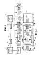
- FIG. 3 a portion of the buffer (buffer 14 of Fig. 1) is illustrated.
- a plurality of transmitting means are shown as controlled transmitters 44 and 46. These transmitters are also referred to as a third preselected set from the plurality of transmitting means.
- the ellipses between transmitters 44.and 46 indicate that duplicate transmitters have been deleted to simplify the illustration.
- the output lines of transmitters 44 and 46 are balanced, complementary data lines CLSla and CLSNa, respectively,which are part of the control lines 42 of Fig. 1.
- Transmitters 44 and 46 are AND gates whose pairs of inputs are commonly connected to lines LSla and LSNa, respectively, the latter lines being referred to as a plurality of control lines connecting to computer SL.
- Line LSNa is a halt line which also connects to the inputs of inverters 48 and 50 whose outputs are identified herein as terminals H2 and HI, respectively.
- Terminal Hl also connects to the input of inverter 52 whose output terminal is identified as terminal BH.
- Transmitters 44 and 46 are commercially available line drivers that can replicate the digital signal on their inputs,provided they receive an enabling signal from amplifiers 54 and 56, respectively.
- the inputs of amplifiers 54 and 56 are commonly connected to control line VPa to receive a signal generated by computer SL (Fig. 1). It will be appreciated that the other transmitters as employed in this figure, each have a similar amplifier whose input is commonly connected to line VPa.
- Transmitters 58 and 60 are members of a larger group as indicated by the ellipses between them. Those unillustrated members were deleted to simplify the illustration. Transmitters 58 and 60 connect to control lines LSlb and LSNb, respectively,of the slave computer SL (Fig. 1). Transmitters 58 and 60 also have associated therewith driving amplifiers 62 and 64, respectively, whose inputs are commonly connected to control line VPb. An enabling signal on line VPb causes transmitters 58 and 60 to relay the data on lines LSlb and LSNb to their respective output lines, CLSlb and CLSNb. The latter lines are part of control line group 42 (Fig. 2).
- a plurality of controlled receiving means is shown herein as a third preselected group of receivers 66 and 68 whose balanced inputs are identified as lines CLMlb and CLMNb, respectively (from lines 42 of Fig. 2).
- Receivers.66 and 68 are members of a larger group, as suggested by the ellipses between them.
- Receivers 66 and 68 can relay input data to their output lines LMlb and LMNb, respectively, when a driving signal is connected to their common enabling terminal VPb.
- Terminal VPb is a control line of computer SL (Fig. 1).
- Lines LMlb and LMNb are control lines of the slave computer SL (Fig. 1).
- receivers 66 and 68 are phased oppositely from transmitters 58 and 60. Thus, when the signal on line VPb is high receivers 66 and 68 are operable while transmitters 58 and 60 operate when the signal line VPb is low.
- receivers or transmitters illustrated in this application present a high output impedance. It will also be appreciated that the illustrated receivers and transmitters can be operated in different time intervals by being driven by different control lines.
- a schematic is given that is essentially identical to that of Fig. 4 except that it connects to different lines.
- lines VPb, LMlb, LMNb, LSlb, LSNb, CLMlb, CLMNb, CLSlb and CLSNb are replaced herein by lines VPc, HLX, BC, LSlc, LSNc, HALT, MBC, CLSlc and CLSNc, respectively.
- transmitters and receivers previously identified as elements 66, 68, 58 and 60 are identified herein as elements 70, 72, 74 and 76, respectively.
- the input of inverter 78 is shown herein connected to line BC, its output connecting to terminal PC.
- line HALT conveys a command for computer SL (Fig. 1) to halt, transmitted from master computer MC (Fig. 1).
- This halt signal is applied by receiver 70 to line HLX thereby providing slave computer (SL) an indication that a request to halt has been entered for the purpose of transferring data.
- a second preselected set from a plurality of transmitting means is shown herein as transmitters 80 and 82 having balanced output lines CX1 and CXN, respectively.
- Transmitters 80 and 82 are in the form of AND gates whose input pairs are connected to data lines Xl and XN, respectively.
- a second preselected group from a plurality of receiving means is shown herein as receivers 84 and 86,having balanced inputs also connected to lines CX1 and CXN, respectively. It will be noted therefore that the output of the illustrated transmitters are connected in parallel with the inputs of their associated, respective receivers.
- the outputs of receivers 84 and 86 are separately connected to the inputs of buffer amplifiers 88 and 90, respectively.
- the output of amplifiers 88 and 90 are connected to data lines Xl and XN, respectively. Being connected in this fashion, it will be appreciated that the receivers and transmitters are connected in antiparallel to allow bilateral communication. It will be noted that lines CXl and CXN are members of the group CX1-21 of Fig. 2, whereas lines Xl and XN are part of the data lines connected to slave computer SL of Fig. 1. Transmitters 80 and 82 have enabling terminals connected to previously illustrated line BC for rendering the transmitters operative or inoperative. Similarly, receivers 84 and 86 have enabling terminals commonly connected to previously illustrated line BC. It will be appreciated that since line BC is the inverse of line BC, when the receivers are enabled the transmitters are not, and vice versa. Connected in this fashion, the equipment can perform simplex communication.
- group 92 and 94 two, essentially identical, antiparallel configurations are shown: group 92 and 94. It will further be appreciated that these two groups are replicated to allow processing of as many data lines as is necessary, this feature being indicated by the ellipses between groups 92 and 94 and their associated lines.
- the enabling terminals of such additional receivers will be commonly connected to line BC while the enabling terminals of additional transmitters will be commonly connected to BC.
- a first preselected set from a plurality of transmitting means is shown herein as transmitters 96 and 98.
- a first preselected group from a predetermined set of controlled receiving means is shown herein as receivers 100 and 102.
- the circuit diagram herein is identical to that of Fig. 6 except that the circuit points are connected to different lines. Specifically, previously identified lines BC, X1, BC, XN, CX1 and CXN are replaced by lines BH, A1, H1, AN, CAl and CAN, respectively.
- the transmit enable terminals of transmitters 96 and 98 connect to halt line BH which was previously described in Fig. 3, as was, halt line HI.
- Elements 96, 104, 100, 98, 106 and 102 of this figure correspond to elements 80, 88, 84, 82, 90 and 86, respectively, of Fig. 6. It will again be appreciated that because lines BH and H1 are oppositely phased, either the receivers or the transmitters will be operative but not both. This feature allows for simplex communication to address lines A1-AN of computer SL (Fig. 1).
- receivers 108 and 110 a portion of a predetermined set from a plurality of controlled receiving means is shown herein as receivers 108 and 110 whose balanced inputs connect to lines CAN+1 and CAN+M, respectively.
- the outputs of receivers 108 and 110 connect to address lines AN+1 and AN+M.
- the receive terminals of receivers 108 and 110 are commonly connected to previously described halt line H2. Again, additional receivers are suggested by the ellipses between the receivers and their input and output lines.
- a unit under test 24 is connected through lines 25 to the measuring and stimulating devices 22.
- programming instructions can be fed into slave computer SL by operating a tape reader 18 for quick feeding or by actuating manual switches 20 to transmit individual programming words.
- slave computer SL can through line printer 16 or teletypewriter 18 transmit acknowledging responses, inquiries and error.signals.
- master computer MC it is usually simpler for master computer MC to transmit progam- ming information through link 10 and buffer 14.
- master computer MC is, in this embodiment, a large, general-purpose computer employing many interactive devices such as cathode ray tube 12, initial programming and debugging can be performed more simply and rapidly by dispatching programming instructions from master computer MC.
- a keyboard associated with cathode ray tube 12 can be used to assemble instructions while its video screen displays the program as well as programming errors.
- Master computer MC transmits this program over lines 26 through interface 28 (Fig. 2).
- Microcomputer 30 then sends corresponding control signals on lines 34 and address signals on lines AD directing the transmittal of this program along lines LA/B and into memory 32. Subsequently, the program is retransmitted on lines LA/B through interface 38 onto lines CX1-21 to program slave computer SL (Fig. 1).
- master computer MC (Fig. 1) may be used to troubleshoot a unit 24.
- the slave computer SL can operate-the instruments 22 and thereby compile data on the responses and operating perameters of unit 24. Thereafter, an inspector may wish to perform additional tests to refine his diagnosis. Accordingly, an inspector may send from master computer MC,instructions to operate certain instruments and stimulating devices in rack 22 and return the associated measurements, as follows: Instructions are initially conveyed on lines 26 (Fig. 2) through interface 28, microprocessor 30 and interface 38, to lines 40. The instructions thus conveyed are coupled through buffer 14 (Fig. 1) to cause slave computer SL to operate the appropriate instruments and stimulating devices in rack 22 (Fig. 1), perform the requested tests and return on lines 23 the requested measurements.
- Slave computer SL then conveys this information through buffer 14 and line 40 to' link 10. This returning information is transmitted on information lines CX1-21 through interface 38 (Fig. 2) onto data lines LEXO-15. Thereafter, the information is relayed through interface 28 to master computer MC on lines 26 so they may be displayed on cathode ray tube 12 (Fig. 1).
- FIG. 1 Another desirable feature provided by the system of Figs. 1 and 2 is the display and rewriting of information in the memory of slave computer SL. Also, real time debugging can be performed by means of the master computer. In both of the latter instances, the flow and return of instructions and data is similar to that previously described.
- buffer 14 (Fig. 1) must exchange data at an apprpriate time to avoid interfering with internally circulating information on the data and address lines of slave computer SL (Fig. 1).
- slave computer SL can receive or transmit five different classes of control signals.
- the first three classes are the computer control signals handled by the apparatus of Figs. 3-5.
- An enabling signal on line VPa from slave computer SL (Fig. 1) will allow transmission of control signals from the slave computer, including the halt signal of line LSNa (Fig. 3).
- an enabling signal on line VPb (Fig. 4) from slave computer SL (Fig. 1) will allow the master computer MC to either receive from or transmit to slave computer SL computer control signals.
- an enabling signal on line VPc (Fig. 5) from slave computer SL(Fig. 1) will allow the master computer MC to either receive from or transmit to slave computer SL computer control signals, including a strobing signal on lines BC and BC.
- master computer MC (Fig. 1) initiates and directs the direction of an exchange of data on data lines CXl-CXN and X1-XN (Fig. 6) of the master and slave computer.
- a final class of signals are those being transmitted to or from address lines A1-AN and AN+1-AN+M (Figs. 7 and 8).
- This halt signal can be self- initiated or can be in response to a halt request on lines HALT (Fig. 5) from master computer MC (Fig. 1). In any event,.
- a halt signal on line LSNa (Fig. 3) is coupled through inverters 48, 50 and 52 to the address exchanging equipment of Figs. 7 and 8.
- transmitters and receivers may be added, depending upon the number of simultaneous bits handled by the various computers.
- these receivers and transmitters can be segregated and separately enabled depending upon the nature of the exchange of information between the computers.
- different groups of receivers and transmitters can be controlled by the illustrated halt signals depending upon the sensitivity of the associated information lines to the arrival of external signals when a computer is not halted. It is also expected that for situations where simultaneous exchange of data (duplex communication) is required, either the receivers and transmitters will be separated (non-parallel) or multiplexing techniques will be used.
- receivers and transmitters formed of integrated circuits are suggested herein, in other embodiments, discrete components may be employed. Alternatively, other embodiments may employ a larger scale of integration thereby containing a larger portion of the circuitry in a single pacakge. In other embodiments, the command to operate certain receivers or transmitters might come from a different computer (a slave computer may be influential instead of the master computer and vice versa). It is also expected, that numerous circuit modifications and component substitutions can be invoked depending upon the desired speed, capacity, power, noise immunity, etc.
Abstract
A buffer (14) can exchange data between a computer (SL) having a plurality of lines (41) and a device (MC). One of these lines (BH, H1, H2), a halt line, can transmit a halt signal when the computer has halted. The buffer (14) includes a plurality of transmitters (44, 46, 58, 60, 74, 76, 80, 82, 96, 98) and a plurality of controlled receivers (66, 68, 70, 72, 84, 86, 100, 102,108, 110). A halt transmitter (46) is included among the plurality of transmitters. The transmitters are separately connected to predetermined respective ones (LS1a, LSNa, LS1 b, LSNb, LS1c, LSNc, X1, XN, A1, AN) of the plurality of lines for transmitting their signals to the device (MC). The halt transmitter (46) is connected to the halt line (BH, H1, H2) for transmitting the halt signal to the device (MC). The receivers are connected between the device (MC) and given respective ones of the plurality of lines (LM1b, LMNb, HLX, BC, X1, XN, A1, AN, AN+1, AN+M) for coupling to them signals from the device (MC). Each one of a predetermined set (100, 102) from the plurality of receivers has a receive terminal (H1) commonly connected to the halt line (H1) for enabling operation of this predetermined set (100, 102) in response to the halt signal.
Description
- The present invention relates to data buffers and, in particular, to devices for exchanging information with a computer when it is halted.
- It is known to transmit digital information over bus lines which terminate in receiving and transmitting circuits. These receivers and transmitters typically are integrated circuit designed to restore the signal level which may have become attenuated or noisy over a relatively long cable. Such receivers and transmitters can exchange digital data and can be effectively isolated from its associated bus line by a control signal. It is also known to halt or interrupt a computer so that certain important functions can be performed.
- A disadvantage with known systems is their failure to design the buffers into the system to allow gating of data so that it is received at an appropriate time, for example, when the computer is halted. Known systems also fail to consider a buffer system whereby simplex communication can be effected in an orderly fashion.
- Accordingly, there is a need for simple and effective buffer for restoring digital signal levels while allowing an orderly transfer of data to and from a computer.
- In accordance with the illustrative embodiment demonstrating features and advantages of the present invention, there is provided a buffer for exchanging data between a device and a computer. The computer has a plurality of lines including a halt line.. This halt line can transmit a halt signal when the computer has halted. The buffer includes a plurality of transmitting means (including a halt transmitter) and a plurality of controlled receiving means. The transmitting means are separately connected to predetermined respective ones of the plurality of lines and respond to the plurality of lines for transmitting their signals to the device. The halt transmitter is connected to the halt line for transmitting the halt signal to the device. The controlled receiving means are connected between the device and given respective ones of the plurality of lines for coupling to them signals from the device. Each one of a predetermined set from the plurality of receiving means has a receive terminal. The receive terminal is commonly connected to the halt line for enabling operation of the predetermined set in response to the halt signal.
- Also, in accordance with the present invention there is provided a method for exchanging data between a device and a computer. This computer has a plurality of lines including a halt line. The halt line is operable to convey a halt signal when the computer has halted. The method includes the step of transmitting signals from predetermined respective ones of the plurality of lines to the device. The method also includes the step of coupling signals from the device to given respective ones of the plurality of lines when a halt signal is provided by the computer on the halt line.
- By providing apparatus and methods of the foregoing type, an effective technique is provided for buffering data into and out of a computer in an orderly fashion. In a preferred embodiment, each member of a group among the address lines of the computer is connected to a parallel(pair) combination of a receiver and transmitter. Each of these pairs is controlled by a halt line from the computer.
- The halt line is inverted to produce two signals: a direct and an inverted signal. The direct signal is used to operate a transmitter for forwarding information from the address lines of the computer. The inverted halt signal is used for operating receivers that couple information onto the address lines of the computer. Also in that preferred embodiment, certain ones of the address lines are connected to receivers which are not paralleled with transmitters.
- Also in one embodiment, the receivers and transmitters exchange control signals with the computer.
- These receivers and transmitters are rendered operable and inoperable by signals internally generated by the computer.
- It is contemplated that the buffer may be used to exchange data with the computer as it operates a test instrument that is diagnosing a test unit. The computer can respond to information received through the buffer to operate the test instrument. In turn, the computer can relay information gathered by the test instrument out through the buffer. The data thus requested and received can be used by an inspector to troubleshoot or evaluate a test unit.
- Also in a preferred embodiment, a transmitter is connected to the halt -line for forwarding that halt signal to an external device. In this embodiment, the external device is another computer used to control the computer transmitting the halt signal.
- The above brief description as well as other objects, features and advantages of the present. invention will be more fully appreciated by reference to the following detailed description of a presently preferred but nonetheless illustrative embodiment in accordance with the present invention when taken in conjunction with the accompanying drawings wherein:
- Fig. 1 is a block diagram of a data system including a buffer according to the present invention;
- Fig. 2 is a more detailed block diagram of the link of Fig. 1;
- Fig. 3 is a schematic diagram of a first portion of the buffer in Fig. 1;
- Fig. 4 is a schematic diagram of a second portion of the buffer of Fig. 1;
- Fig.`5 is a schematic diagram of a third portion of the buffer of Fig. 1;
- Fig. 6 is a schematic diagram of a fourth portion of the buffer of Fig. 1;
- Fig. 7 is a schematic diagram of a fifth portion of the buffer of Fig. 1; and
- Fig. 8 is a schematic diagram of a sixth portion of the buffer of Fig. 1.
- Referring to Fig. 1,
link 10 is connected to a device, shown herein as master computer MC, by a plurality oflines 26. Computer MC is a general-purpose computer including as illustrated: memory, a central processing unit (CPU) and an input/output port (I/O). Master computer MC is shown connected to a display device, in this embodiment, cathode ray tube 12. -
Link 10 is arranged to exchange data between master computer MC and slave computer SL. Since slave computer SL is located at a significant distance from link 10 a relativelylong cable 40 comprising a plurality of lines connects betweenlink 10 andbuffer 14.Buffer 14 employs transmitting and receiving devices for restoring the signal levels that may be attenuated throughcable 40.Buffer 14 is shown connecting directly to slave computerSL through a plurality of lines, whose signals correspond to the information oncable 40. Slave computer SL is shown with a slave memory having a plurality of memory cells, a central processing unit (CPU) and an input/output port (I/O). Slave computer SL is shown connected through its input/output port andlines 23 to a plurality of peripherals. Four such peripherals connected to it are conventional line printer 16, teletypewriter 18,magnetic tape memory 15 and computer displays 17. Also, connected in this fashion is a manual programmer shown herein as plurality of manual switches 20, one for each relevant bit. Switches 20 can be used to transmit a data word to slave computer SL for the purpose of controlling pro- : gramming, reprogramming or debugging programs of slave computer SL. Also connected by lines.23 to slave computer SL are a rack of test instruments and stimulating devices 22. These test instruments may include voltmeters, frequency counters, ammeters, etc..These instruments can be operated by the signals transmitted onlines 23 by slave computer SL to cause instruments 22 to relay back onlines 23 operating parameters measured by them. Instruments 22 connect to a unit undertest 24 through a test terminal shown herein as interconnectinglines 25. The stimulating devices in block 22 may include current sources and voltage sources of various types which provide through probes inlines 25 stimulating signals to test the performance ofunit 24. - Referring to Fig. 2, previously illustrated
link 10 is shown herein in further detail. A group oflines 26 that are internal to the previously mentioned master computer (computer MC of Fig. 1) connect to interface device 28 which is also internal to that master computer.Lines 26 consists of conventional control lines 26A,data lines 26B and address lines 26C. Interface 28 connects to address lines AD which are bussed to amicroprocessor 30 and memory subsystem 32, the latter comprising a group of read only and random access memories.Microprocessor 30 and memory'32 can exchange data with data line LA/B which also connects to interface 28. A group ofcontrol lines 34 frommicroprocessor 30 connects to interface 28.Microprocessor 30 also has another group ofcontrol lines 36 separately connected to interface 38.Interface 38 has a group of sixteen data lines LEXO-15 which together with data lines LA/B form a group referred to herein as a plurality of information lines. Theother lines 40 frominterface 38 connect to the previously mentioned slave computer (computer SL of Fig. 1).Lines 40 includes another plurality of information lines CXl-21 (comprising 21 lines in this embodiment)control lines 42 and fifteen address lines CA1-15.Interface 38 transmits data on lines LEXO-15 and CAl-15. Interface .38 also exchanges data with data lines LA/B and CX1-21. It will be noted that in this embodiment, the foregoing data lines are incompatible. - Referring to Fig. 3, a portion of the buffer (buffer 14 of Fig. 1) is illustrated. A plurality of transmitting means are shown as controlled
transmitters transmitters control lines 42 of Fig. 1.Transmitters inverters -
Transmitters amplifiers amplifiers - Referring to Fig. 4, additional members of the previously mentioned third preselected set are shown herein as
transmitters Transmitters Transmitters Transmitters amplifiers transmitters - . A plurality of controlled receiving means is shown herein as a third preselected group of
receivers lines 42 of Fig. 2). Receivers.66 and 68 are members of a larger group, as suggested by the ellipses between them.Receivers receivers transmitters high receivers transmitters - It will be understood that when disabled, the receivers or transmitters illustrated in this application present a high output impedance. It will also be appreciated that the illustrated receivers and transmitters can be operated in different time intervals by being driven by different control lines.
- Referring to Fig. 5, a schematic is given that is essentially identical to that of Fig. 4 except that it connects to different lines. In particular, the previously mentioned lines VPb, LMlb, LMNb, LSlb, LSNb, CLMlb, CLMNb, CLSlb and CLSNb are replaced herein by lines VPc, HLX, BC, LSlc, LSNc, HALT, MBC, CLSlc and CLSNc, respectively. Similarly, transmitters and receivers previously identified as
elements elements inverter 78 is shown herein connected to line BC, its output connecting to terminal PC. - In this embodiment, line HALT conveys a command for computer SL (Fig. 1) to halt, transmitted from master computer MC (Fig. 1). This halt signal is applied by
receiver 70 to line HLX thereby providing slave computer (SL) an indication that a request to halt has been entered for the purpose of transferring data. - Referring to Fig. 6, a second preselected set from a plurality of transmitting means is shown herein as
transmitters 80 and 82 having balanced output lines CX1 and CXN, respectively.Transmitters 80 and 82 are in the form of AND gates whose input pairs are connected to data lines Xl and XN, respectively. A second preselected group from a plurality of receiving means is shown herein asreceivers receivers buffer amplifiers 88 and 90, respectively. The output ofamplifiers 88 and 90 are connected to data lines Xl and XN, respectively. Being connected in this fashion, it will be appreciated that the receivers and transmitters are connected in antiparallel to allow bilateral communication. It will be noted that lines CXl and CXN are members of the group CX1-21 of Fig. 2, whereas lines Xl and XN are part of the data lines connected to slave computer SL of Fig. 1.Transmitters 80 and 82 have enabling terminals connected to previously illustrated line BC for rendering the transmitters operative or inoperative. Similarly,receivers - It will further be appreciated that two, essentially identical, antiparallel configurations are shown: group 92 and 94. It will further be appreciated that these two groups are replicated to allow processing of as many data lines as is necessary, this feature being indicated by the ellipses between groups 92 and 94 and their associated lines. The enabling terminals of such additional receivers will be commonly connected to line BC while the enabling terminals of additional transmitters will be commonly connected to BC.
- Referring to Fig. 7, a first preselected set from a plurality of transmitting means is shown herein as
transmitters receivers transmitters Elements elements - Referring to Fig. 8, a portion of a predetermined set from a plurality of controlled receiving means is shown herein as
receivers 108 and 110 whose balanced inputs connect to lines CAN+1 and CAN+M, respectively. The outputs ofreceivers 108 and 110 connect to address lines AN+1 and AN+M. The receive terminals ofreceivers 108 and 110 are commonly connected to previously described halt line H2. Again, additional receivers are suggested by the ellipses between the receivers and their input and output lines. - To facilitate an understanding of the principles associated with the foregoing apparatus,its operation will be briefly described. Initially, the general operation of the system of Figs. 1 and 2 will be reviewed before considering the buffer circuitry in Figs. 3-8. A unit under
test 24 is connected throughlines 25 to the measuring and stimulating devices 22. Before starting, if desired, programming instructions can be fed into slave computer SL by operating a tape reader 18 for quick feeding or by actuating manual switches 20 to transmit individual programming words. In this mode, slave computer SL can through line printer 16 or teletypewriter 18 transmit acknowledging responses, inquiries and error.signals. However, it is usually simpler for master computer MC to transmit progam- ming information throughlink 10 andbuffer 14. - Because master computer MC is, in this embodiment, a large, general-purpose computer employing many interactive devices such as cathode ray tube 12, initial programming and debugging can be performed more simply and rapidly by dispatching programming instructions from master computer MC. A keyboard associated with cathode ray tube 12 can be used to assemble instructions while its video screen displays the program as well as programming errors. Master computer MC transmits this program over
lines 26 through interface 28 (Fig. 2).Microcomputer 30 then sends corresponding control signals onlines 34 and address signals on lines AD directing the transmittal of this program along lines LA/B and into memory 32. Subsequently, the program is retransmitted on lines LA/B throughinterface 38 onto lines CX1-21 to program slave computer SL (Fig. 1). - Also, master computer MC (Fig. 1) may be used to troubleshoot a
unit 24. The slave computer SL can operate-the instruments 22 and thereby compile data on the responses and operating perameters ofunit 24. Thereafter, an inspector may wish to perform additional tests to refine his diagnosis. Accordingly, an inspector may send from master computer MC,instructions to operate certain instruments and stimulating devices in rack 22 and return the associated measurements, as follows: Instructions are initially conveyed on lines 26 (Fig. 2) through interface 28,microprocessor 30 andinterface 38, tolines 40. The instructions thus conveyed are coupled through buffer 14 (Fig. 1) to cause slave computer SL to operate the appropriate instruments and stimulating devices in rack 22 (Fig. 1), perform the requested tests and return onlines 23 the requested measurements. Slave computer SL then conveys this information throughbuffer 14 andline 40 to' link 10. This returning information is transmitted on information lines CX1-21 through interface 38 (Fig. 2) onto data lines LEXO-15. Thereafter, the information is relayed through interface 28 to master computer MC onlines 26 so they may be displayed on cathode ray tube 12 (Fig. 1). - Another desirable feature provided by the system of Figs. 1 and 2 is the display and rewriting of information in the memory of slave computer SL. Also, real time debugging can be performed by means of the master computer. In both of the latter instances, the flow and return of instructions and data is similar to that previously described.
- To perform the foregoing functions buffer 14 (Fig. 1) must exchange data at an apprpriate time to avoid interfering with internally circulating information on the data and address lines of slave computer SL (Fig. 1). 'In this embodiment, slave computer SL can receive or transmit five different classes of control signals.
- The first three classes are the computer control signals handled by the apparatus of Figs. 3-5. An enabling signal on line VPa from slave computer SL (Fig. 1) will allow transmission of control signals from the slave computer, including the halt signal of line LSNa (Fig. 3). Depending upon its state,an enabling signal on line VPb (Fig. 4) from slave computer SL (Fig. 1) will allow the master computer MC to either receive from or transmit to slave computer SL computer control signals.
- Thirdly, depending upon its state, an enabling signal on line VPc (Fig. 5) from slave computer SL(Fig. 1) will allow the master computer MC to either receive from or transmit to slave computer SL computer control signals, including a strobing signal on lines BC and BC.
- These strobing signals on lines BC and BC, depending upon their state, allow exchange of anotherclass of signals, the data signals of Fig. 6. Thus, in this embodiment, master computer MC (Fig. 1) initiates and directs the direction of an exchange of data on data lines CXl-CXN and X1-XN (Fig. 6) of the master and slave computer.
- A final class of signals are those being transmitted to or from address lines A1-AN and AN+1-AN+M (Figs. 7 and 8). This is a sensitive class of signals and care must be taken to avoid disruption of the slave computer when it is internally processing addresses. Accordingly, this data exchange awaits a halt signal on line LSNa (Fig. 3) from the slave computer. This halt signal can be self- initiated or can be in response to a halt request on lines HALT (Fig. 5) from master computer MC (Fig. 1). In any event,. a halt signal on line LSNa (Fig. 3) is coupled through
inverters transmitters receivers - It is to be appreciated that various modifications may be implemented with respect to the above described preferred embodiment. For example, additional transmitters and receivers may be added, depending upon the number of simultaneous bits handled by the various computers. Also, these receivers and transmitters can be segregated and separately enabled depending upon the nature of the exchange of information between the computers. Furthermore, different groups of receivers and transmitters can be controlled by the illustrated halt signals depending upon the sensitivity of the associated information lines to the arrival of external signals when a computer is not halted. It is also expected that for situations where simultaneous exchange of data (duplex communication) is required, either the receivers and transmitters will be separated (non-parallel) or multiplexing techniques will be used. Also while conventional receivers and transmitters formed of integrated circuits are suggested herein, in other embodiments, discrete components may be employed. Alternatively, other embodiments may employ a larger scale of integration thereby containing a larger portion of the circuitry in a single pacakge. In other embodiments, the command to operate certain receivers or transmitters might come from a different computer (a slave computer may be influential instead of the master computer and vice versa). It is also expected, that numerous circuit modifications and component substitutions can be invoked depending upon the desired speed, capacity, power, noise immunity, etc.
- Obviously, many modifications and variations of the present invention are possible in light of the above teachings. It is therefore to be understood that within the.scope of the appended claims, the invention may be practiced otherwise than as specifically described.
Claims (12)
1. A buffer (14) for exchanging data between a device (MC) and a computer (SL), the latter having a plurality of lines (41) including a halt line (BH, H1, H2), said halt line being operable to transmit a halt signal when said computer (SL) has halted, said buffer (14) comprising :
a plurality of transmitting means (44, 46, 58, 60, 74, 76, 80, 82, 96, 98), including a halt transmitter (46), each separately connected to predetermined respective ones (LS1a, LSNa, LSlb, LSNb, LS1c, LSNc, X1, XN, A1, AN of said plurality of lines for transmitting their signals to said device (MC), said halt transmitter (46) being connected to said halt line (BH, H1, H2) for transmitting said halt signal to said device (MC) ; and
a plurality of controlled receiving means (66, 68, 70, 72, 84, 86, 100, 102, 108, 110) connected between said device (MC) and given respective ones (LMlb, LMNb, HLX, BC, X1, SN, A1, AN, AN+1, AN+M) of said plurality of lines for coupling to them signals from said device (MC), each one of a predetermined set (100, 102) from said plurality of receiving means having a receive terminal (H1) commonly connected to said halt line (HI) for enabling operation of said predetermined set (100, 102) in response to said halt signal.
2. A buffer (14) according to claim 1, wherein a first preselected set (96, 98) from said plurality of transmitting means are connected in antiparallel with a first preselected group (100, 102) from of said plurality of controlled receiving means to allow simplex communication.
3. A buffer (14) according to claim 2, wherein those (A1, AN) of said given respective ones of said lines connecting to said first preselected group (100, 102) comprise address lines (A1, AN) for said computer.(SL).
4. A buffer (14) according to claim 2, wherein each of said first preselected set (96, 98) includes a transmit terminal (BH) commonly connected to said halt line (BH) for transmitting in response to said halt signal but at a time different from when said predetermined set (100, 102) is enabled to operate by said halt signal.
5. A buffer (14) according to claim 2, wherein a second preselected set (80, 82) from said plurality of transmitting means are connected in antiparallel with a second preselected group (84, 86) from said plurality of controlled receiving means to allow simplex communication.
6. A buffer (14) according to claim 5, wherein those (X1, XN) of said given respective ones of said lines connecting to said second preselected group (84, 86) comprise data lines (X1, XN) of said computer (SL).
7. A buffer (14) according to claim 6, wherein said plurality of lines includes a plurality of control lines (LS1a, LSNa, LM1b, LMNb, LS1b, LSNb, HLX, BC, LS1c, LSNc), and wherein a third preselected set (44, 46, 58, 60, 74, 76) from said plurality of transmitting means are connected to a portion (LS1a, LSNa, LSlb, LSNb, LS1c, LSNc) of said control lines, the remaining ones (LM1b, LMNb, HLX, BC) of said control lines being connected to a third preselected group (66, 68, 70, 72) from said plurality of controlled receiving means.
8. A buffered test system for testing a unit (24) with a re Jte device (MC), comprising :
a test instrument (22) having a test terminal (25) arranged to be connected to said unit (24) to measure an operating parameter thereof ;
a computer (SL) having a plurality .of lines (41, 23), at least one (23) of them being connected to said test instrument for sending it a signal to commence operation and for receiving measurement signals ;
a plurality of transmitting means (44, 46, 58, 60, 74, 76, 80, 82, 96, 98) separately connected to predetermined respective ones (LS1a, LSNa, LS1b, LSNb, LS1c, LSNc, X1, XN, A1, AN) of said plurality of lines for transmitting their signal to said device (MC) ; and
a plurality of controlled receiving means (66, 68, 70, 72, 84, 86, 100, 102, 108 110) connected between said device (MC) and given respective ones (LM1b, LMNb, HLX, BC, X1, XN, A1, AN, AN+1, AN+M) of said plurality of lines for coupling to them signals from said device (MC).
9. A buffered test system according to claim 8, wherein said plurality of lines-includes halt line (BH, H1, H2) operable to transmit a halt signal when said computer (SL) has halted, said plurality of transmitting means including a halt transmitter (46) connected to said halt line (BH, H1, H2) for transmitting said halt signal to said device (MC), each of a predetermined set (100, 102 from said plurality of receiving means having a receive terminal (H1) commonly connected to said halt line (H1) for enabling operation of said predetermined set (100, 102).
10, A buffered test system according to claim 1, 2 or 3, wherein said device (MC) is a digital computing device.
11. A method for exchanging data between a device (MC) and a computer (SL) having a plurality of lines (41, 23) including a halt line (BH, H1, H2) operable to convey a halt signal when said computer has halted, comprising the steps of :
transmitting signals from predetermined respective ones (A1, AN) of said plurality of lines to said device ; and
coupling signals from said device (MC) to given respective ones (A1, AN) of said plurality of lines when a halt signal is provided by said computer (SL) on said halt line (BH, H1, H2).
12. The method of claim 11 further employing a test instrument (22) and further comprising the steps of :
rendering said test instrument (22) operative when a predetermined signal is provided on said plurality of lines (41, 23) by said computer (SL) and
relaying measurements obtained by said instruments (22) through said plurality of lines (23, 41).
Applications Claiming Priority (2)
| Application Number | Priority Date | Filing Date | Title |
|---|---|---|---|
| US06/275,005 US4429362A (en) | 1981-06-18 | 1981-06-18 | Data buffer operating in response to computer halt signal |
| US275005 | 1981-06-18 |
Publications (2)
| Publication Number | Publication Date |
|---|---|
| EP0068991A2 true EP0068991A2 (en) | 1983-01-05 |
| EP0068991A3 EP0068991A3 (en) | 1985-11-27 |
Family
ID=23050512
Family Applications (1)
| Application Number | Title | Priority Date | Filing Date |
|---|---|---|---|
| EP82401113A Withdrawn EP0068991A3 (en) | 1981-06-18 | 1982-06-18 | Data buffer |
Country Status (4)
| Country | Link |
|---|---|
| US (1) | US4429362A (en) |
| EP (1) | EP0068991A3 (en) |
| JP (1) | JPS582922A (en) |
| IL (1) | IL65830A (en) |
Cited By (2)
| Publication number | Priority date | Publication date | Assignee | Title |
|---|---|---|---|---|
| GB2187004A (en) * | 1986-02-20 | 1987-08-26 | Stc Plc | Modular vision system |
| GB2300540A (en) * | 1995-03-31 | 1996-11-06 | Int Mobile Satellite Org | Digital communications link interface |
Families Citing this family (9)
| Publication number | Priority date | Publication date | Assignee | Title |
|---|---|---|---|---|
| JPS6381554A (en) * | 1986-09-25 | 1988-04-12 | Canon Inc | Electronic device handling peripheral equipment capable of replacement |
| DE3731018A1 (en) * | 1987-09-11 | 1989-03-30 | Licentia Gmbh | Method of matching the running time of bus or input/output lines in digital computers |
| US5123092A (en) * | 1988-10-21 | 1992-06-16 | Zenith Data Systems Corporation | External expansion bus interface |
| ITMO20030329A1 (en) * | 2003-12-03 | 2005-06-04 | Leophorm S R L | CLEANING BRUSH FOR SURFACE WASHING. |
| US20060123586A1 (en) * | 2004-12-10 | 2006-06-15 | Wegelin Jackson W | Extractor stretch hose |
| US7657964B2 (en) * | 2004-12-10 | 2010-02-09 | Techtronic Floor Care Technology Limited | Lift off tank handle latch |
| US7870637B2 (en) * | 2004-12-10 | 2011-01-18 | Techtronic Floor Care Technology Limited | Stacked tank arrangement for a cleaning apparatus |
| US7877836B2 (en) * | 2004-12-10 | 2011-02-01 | Techtronic Floor Care Technology Limited | Extractor control apparatus |
| US7725983B2 (en) * | 2004-12-10 | 2010-06-01 | Techtronic Floor Care Technology Limited | Recovery tank arrangement for a cleaning apparatus |
Citations (2)
| Publication number | Priority date | Publication date | Assignee | Title |
|---|---|---|---|---|
| US4069510A (en) * | 1974-10-30 | 1978-01-17 | Motorola, Inc. | Interrupt status register for interface adaptor chip |
| DE2713304A1 (en) * | 1977-03-25 | 1978-09-28 | Siemens Ag | Multiple computer control system - allows separate computers to correspond using tri-state interface circuits between address and data buses |
Family Cites Families (3)
| Publication number | Priority date | Publication date | Assignee | Title |
|---|---|---|---|---|
| JPS5178628A (en) * | 1975-03-31 | 1976-07-08 | Nippon Signal Co Ltd | |
| JPS55164922A (en) * | 1979-06-08 | 1980-12-23 | Toshiba Corp | Multimicrocomputer |
| JPS5671129A (en) * | 1979-11-15 | 1981-06-13 | Fujitsu Ltd | Data processing system |
-
1981
- 1981-06-18 US US06/275,005 patent/US4429362A/en not_active Expired - Fee Related
-
1982
- 1982-05-19 IL IL65830A patent/IL65830A/en unknown
- 1982-06-11 JP JP57099416A patent/JPS582922A/en active Pending
- 1982-06-18 EP EP82401113A patent/EP0068991A3/en not_active Withdrawn
Patent Citations (2)
| Publication number | Priority date | Publication date | Assignee | Title |
|---|---|---|---|---|
| US4069510A (en) * | 1974-10-30 | 1978-01-17 | Motorola, Inc. | Interrupt status register for interface adaptor chip |
| DE2713304A1 (en) * | 1977-03-25 | 1978-09-28 | Siemens Ag | Multiple computer control system - allows separate computers to correspond using tri-state interface circuits between address and data buses |
Non-Patent Citations (2)
| Title |
|---|
| JOURNAL OF PHYSICS E; SCIENTIFIC INSTRUMENTS, vol. 9, no. 10, October 1976, pages 794-802, London, GB; E.J. MILLETT: "Digital techniques in laboratory automation" * |
| PROCEEDINGS OF THE IEEE, vol. 63, no. 10, October 1975, pages 1509-1513, New York, US; A.A. GUIDO et al.: "Interactive laboratory automation aid: the research device coupler" * |
Cited By (5)
| Publication number | Priority date | Publication date | Assignee | Title |
|---|---|---|---|---|
| GB2187004A (en) * | 1986-02-20 | 1987-08-26 | Stc Plc | Modular vision system |
| GB2300540A (en) * | 1995-03-31 | 1996-11-06 | Int Mobile Satellite Org | Digital communications link interface |
| GB2300540B (en) * | 1995-03-31 | 1999-10-20 | Int Mobile Satellite Org | Communication method and apparatus |
| GB2337665A (en) * | 1995-03-31 | 1999-11-24 | Inmarsat Ltd | Communication method and apparatus |
| GB2337665B (en) * | 1995-03-31 | 2000-02-16 | Inmarsat Ltd | Communication method and apparatus |
Also Published As
| Publication number | Publication date |
|---|---|
| JPS582922A (en) | 1983-01-08 |
| IL65830A (en) | 1985-06-30 |
| US4429362A (en) | 1984-01-31 |
| EP0068991A3 (en) | 1985-11-27 |
| IL65830A0 (en) | 1982-08-31 |
Similar Documents
| Publication | Publication Date | Title |
|---|---|---|
| US4057847A (en) | Remote controlled test interface unit | |
| US4296464A (en) | Process control system with local microprocessor control means | |
| US4454577A (en) | Linked data systems | |
| US4514845A (en) | Method and apparatus for bus fault location | |
| EP0063334A1 (en) | Data Processing apparatus for a multiprocessor system | |
| US4167041A (en) | Status reporting | |
| US4429362A (en) | Data buffer operating in response to computer halt signal | |
| US4688171A (en) | Serial bus for master/slave computer system | |
| US4417336A (en) | Method of testing with computers | |
| US4471458A (en) | Computer interface | |
| JPS6226734B2 (en) | ||
| US4066883A (en) | Test vehicle for selectively inserting diagnostic signals into a bus-connected data-processing system | |
| JP2710777B2 (en) | Test circuit for intermediate control unit | |
| JPH0417050A (en) | One-chip microcomputer | |
| JPS6055457A (en) | Channel adapter diagnostic system | |
| JPS6151578A (en) | Fault diagnostic system of electronic circuit device | |
| RU2072788C1 (en) | Apparatus for controlling and restoring technical means intended for medical uses | |
| JP2765659B2 (en) | Self-test method for data processing equipment | |
| JP2645021B2 (en) | Bus abnormality inspection system | |
| JPS59221131A (en) | Data transmission station | |
| CA1129962A (en) | Control panel self-test | |
| JPS63178340A (en) | Integrated circuit for control | |
| JPH11103307A (en) | Transmission system with trigger function and method for measuring time interval of its input output signal | |
| JPS62147554A (en) | Data transfer device | |
| JPS63276137A (en) | Remote maintenance diagnosis system |
Legal Events
| Date | Code | Title | Description |
|---|---|---|---|
| PUAI | Public reference made under article 153(3) epc to a published international application that has entered the european phase |
Free format text: ORIGINAL CODE: 0009012 |
|
| 17P | Request for examination filed |
Effective date: 19820629 |
|
| AK | Designated contracting states |
Designated state(s): DE FR GB IT NL SE |
|
| PUAL | Search report despatched |
Free format text: ORIGINAL CODE: 0009013 |
|
| AK | Designated contracting states |
Designated state(s): DE FR GB IT NL SE |
|
| 17Q | First examination report despatched |
Effective date: 19870317 |
|
| STAA | Information on the status of an ep patent application or granted ep patent |
Free format text: STATUS: THE APPLICATION IS DEEMED TO BE WITHDRAWN |
|
| 18D | Application deemed to be withdrawn |
Effective date: 19870728 |
|
| RIN1 | Information on inventor provided before grant (corrected) |
Inventor name: CONSTANTINI, JOHN JOSEPH |