EP0086907B1 - Recording apparatus - Google Patents
Recording apparatus Download PDFInfo
- Publication number
- EP0086907B1 EP0086907B1 EP82201324A EP82201324A EP0086907B1 EP 0086907 B1 EP0086907 B1 EP 0086907B1 EP 82201324 A EP82201324 A EP 82201324A EP 82201324 A EP82201324 A EP 82201324A EP 0086907 B1 EP0086907 B1 EP 0086907B1
- Authority
- EP
- European Patent Office
- Prior art keywords
- chip
- row
- radiation sources
- rows
- led
- Prior art date
- Legal status (The legal status is an assumption and is not a legal conclusion. Google has not performed a legal analysis and makes no representation as to the accuracy of the status listed.)
- Expired
Links
Images


Classifications
-
- H—ELECTRICITY
- H04—ELECTRIC COMMUNICATION TECHNIQUE
- H04N—PICTORIAL COMMUNICATION, e.g. TELEVISION
- H04N1/00—Scanning, transmission or reproduction of documents or the like, e.g. facsimile transmission; Details thereof
- H04N1/04—Scanning arrangements, i.e. arrangements for the displacement of active reading or reproducing elements relative to the original or reproducing medium, or vice versa
- H04N1/19—Scanning arrangements, i.e. arrangements for the displacement of active reading or reproducing elements relative to the original or reproducing medium, or vice versa using multi-element arrays
- H04N1/195—Scanning arrangements, i.e. arrangements for the displacement of active reading or reproducing elements relative to the original or reproducing medium, or vice versa using multi-element arrays the array comprising a two-dimensional array or a combination of two-dimensional arrays
- H04N1/19505—Scanning picture elements spaced apart from one another in at least one direction
- H04N1/19515—Scanning picture elements spaced apart from one another in at least one direction in two directions
-
- B—PERFORMING OPERATIONS; TRANSPORTING
- B41—PRINTING; LINING MACHINES; TYPEWRITERS; STAMPS
- B41J—TYPEWRITERS; SELECTIVE PRINTING MECHANISMS, i.e. MECHANISMS PRINTING OTHERWISE THAN FROM A FORME; CORRECTION OF TYPOGRAPHICAL ERRORS
- B41J2/00—Typewriters or selective printing mechanisms characterised by the printing or marking process for which they are designed
- B41J2/435—Typewriters or selective printing mechanisms characterised by the printing or marking process for which they are designed characterised by selective application of radiation to a printing material or impression-transfer material
- B41J2/447—Typewriters or selective printing mechanisms characterised by the printing or marking process for which they are designed characterised by selective application of radiation to a printing material or impression-transfer material using arrays of radiation sources
- B41J2/45—Typewriters or selective printing mechanisms characterised by the printing or marking process for which they are designed characterised by selective application of radiation to a printing material or impression-transfer material using arrays of radiation sources using light-emitting diode [LED] or laser arrays
- B41J2/451—Special optical means therefor, e.g. lenses, mirrors, focusing means
-
- G—PHYSICS
- G06—COMPUTING; CALCULATING OR COUNTING
- G06K—GRAPHICAL DATA READING; PRESENTATION OF DATA; RECORD CARRIERS; HANDLING RECORD CARRIERS
- G06K15/00—Arrangements for producing a permanent visual presentation of the output data, e.g. computer output printers
- G06K15/02—Arrangements for producing a permanent visual presentation of the output data, e.g. computer output printers using printers
- G06K15/12—Arrangements for producing a permanent visual presentation of the output data, e.g. computer output printers using printers by photographic printing, e.g. by laser printers
- G06K15/1238—Arrangements for producing a permanent visual presentation of the output data, e.g. computer output printers using printers by photographic printing, e.g. by laser printers simultaneously exposing more than one point
- G06K15/1242—Arrangements for producing a permanent visual presentation of the output data, e.g. computer output printers using printers by photographic printing, e.g. by laser printers simultaneously exposing more than one point on one main scanning line
- G06K15/1247—Arrangements for producing a permanent visual presentation of the output data, e.g. computer output printers using printers by photographic printing, e.g. by laser printers simultaneously exposing more than one point on one main scanning line using an array of light sources, e.g. a linear array
-
- H—ELECTRICITY
- H01—ELECTRIC ELEMENTS
- H01L—SEMICONDUCTOR DEVICES NOT COVERED BY CLASS H10
- H01L25/00—Assemblies consisting of a plurality of individual semiconductor or other solid state devices ; Multistep manufacturing processes thereof
- H01L25/03—Assemblies consisting of a plurality of individual semiconductor or other solid state devices ; Multistep manufacturing processes thereof all the devices being of a type provided for in the same subgroup of groups H01L27/00 - H01L33/00, or in a single subclass of H10K, H10N, e.g. assemblies of rectifier diodes
- H01L25/04—Assemblies consisting of a plurality of individual semiconductor or other solid state devices ; Multistep manufacturing processes thereof all the devices being of a type provided for in the same subgroup of groups H01L27/00 - H01L33/00, or in a single subclass of H10K, H10N, e.g. assemblies of rectifier diodes the devices not having separate containers
- H01L25/075—Assemblies consisting of a plurality of individual semiconductor or other solid state devices ; Multistep manufacturing processes thereof all the devices being of a type provided for in the same subgroup of groups H01L27/00 - H01L33/00, or in a single subclass of H10K, H10N, e.g. assemblies of rectifier diodes the devices not having separate containers the devices being of a type provided for in group H01L33/00
- H01L25/0753—Assemblies consisting of a plurality of individual semiconductor or other solid state devices ; Multistep manufacturing processes thereof all the devices being of a type provided for in the same subgroup of groups H01L27/00 - H01L33/00, or in a single subclass of H10K, H10N, e.g. assemblies of rectifier diodes the devices not having separate containers the devices being of a type provided for in group H01L33/00 the devices being arranged next to each other
-
- H—ELECTRICITY
- H04—ELECTRIC COMMUNICATION TECHNIQUE
- H04N—PICTORIAL COMMUNICATION, e.g. TELEVISION
- H04N1/00—Scanning, transmission or reproduction of documents or the like, e.g. facsimile transmission; Details thereof
- H04N1/024—Details of scanning heads ; Means for illuminating the original
- H04N1/032—Details of scanning heads ; Means for illuminating the original for picture information reproduction
- H04N1/036—Details of scanning heads ; Means for illuminating the original for picture information reproduction for optical reproduction
-
- H—ELECTRICITY
- H04—ELECTRIC COMMUNICATION TECHNIQUE
- H04N—PICTORIAL COMMUNICATION, e.g. TELEVISION
- H04N1/00—Scanning, transmission or reproduction of documents or the like, e.g. facsimile transmission; Details thereof
- H04N1/04—Scanning arrangements, i.e. arrangements for the displacement of active reading or reproducing elements relative to the original or reproducing medium, or vice versa
- H04N1/19—Scanning arrangements, i.e. arrangements for the displacement of active reading or reproducing elements relative to the original or reproducing medium, or vice versa using multi-element arrays
- H04N1/195—Scanning arrangements, i.e. arrangements for the displacement of active reading or reproducing elements relative to the original or reproducing medium, or vice versa using multi-element arrays the array comprising a two-dimensional array or a combination of two-dimensional arrays
- H04N1/19505—Scanning picture elements spaced apart from one another in at least one direction
- H04N1/19521—Arrangements for moving the elements of the array relative to the scanned image or vice versa
- H04N1/19573—Displacing the scanned image
-
- H—ELECTRICITY
- H01—ELECTRIC ELEMENTS
- H01L—SEMICONDUCTOR DEVICES NOT COVERED BY CLASS H10
- H01L2924/00—Indexing scheme for arrangements or methods for connecting or disconnecting semiconductor or solid-state bodies as covered by H01L24/00
- H01L2924/0001—Technical content checked by a classifier
- H01L2924/0002—Not covered by any one of groups H01L24/00, H01L24/00 and H01L2224/00
-
- H—ELECTRICITY
- H01—ELECTRIC ELEMENTS
- H01L—SEMICONDUCTOR DEVICES NOT COVERED BY CLASS H10
- H01L2924/00—Indexing scheme for arrangements or methods for connecting or disconnecting semiconductor or solid-state bodies as covered by H01L24/00
- H01L2924/095—Indexing scheme for arrangements or methods for connecting or disconnecting semiconductor or solid-state bodies as covered by H01L24/00 with a principal constituent of the material being a combination of two or more materials provided in the groups H01L2924/013 - H01L2924/0715
- H01L2924/097—Glass-ceramics, e.g. devitrified glass
- H01L2924/09701—Low temperature co-fired ceramic [LTCC]
Definitions
- the optical transfer means 12 is an elongate element of plastic or the like wherein a plurality of self-focussing fibers are provided, the optical axis of the transfer means, or more correctly the optical plane thereof, passing through the axis of the drum.
Description
- The present invention relates to a recording apparatus for linewise recording information upon a moving photoreceptor.
- Apparatus for recording information upon a moving photoreceptor are known comprising a plurality of stationary pointlike light sources that are arranged in a row that extends transversely of the direction of displacement of a photoreceptor, and that are individually energizable thereby information-wise to expose the photoreceptor in response to delivered information signals as the photoreceptor moves past the row of light sources. The movement of the photoreceptor may occur either continuously or stepwise.
- Thetransferofthe images of the lightsources on the photoreceptor may occur by means of lens arrangements, fiber optics or fiber pipes, self focussing fibers, or the like.
- In the foregoing kind of recording apparatus the light sources must be sufficiently small in order to achieve an acceptable image resolution and the spacing between the images of the light sources transferred to the photoreceptor must be small in order that the visual impression of an uninterrupted transverse line on the photoreceptor can be obtained.
- It is considered in the art that at least 10 light points per mm are required on the photoreceptor, so that the width of a standard DIN A4 photoreceptor size, namely 216 mm, requires a number of at least 2200 discrete light sources.
- A plurality of closely spaced small light sources may be formed by LED's (ligh-emitting diodes) if they are formed as an array of LED's produced on a monolithic chip. Unfortunately, arrays of LED's measuring up to 216 mm cannot be obtained at present, since the manufacturing of the LED's is based on a series of operations carried out on mono-crystalline substrates with a length limited to approximately 50 mm.
- Although it is possible to obtain a defect-free array of LED's on a 50 mm substrate, the series production of such arrays under industrial conditions is not economically feasible. Arrays on a 50 mm substrate normally have to be cut into shorter lengths in order to obtain defect free arrays and experience shows that the average length of defect-free arrays is between about 1 and 10 mm.
- In order to form arrays up to 216 mm a multiplicity of small component arrays have to be assembled in alignment.
- This assembling can occur by mounting small chip sub-units by means of screws to a common bar. This technique is disclosed in US P 4,318,597 to OKI Electric Industry Co., Ltd., relating to an optical printing head for optical printing devices. The disclosed technique has the disadvantage that relatively large supports are required for the chips in order to provide space for the screws, so that considerable spacing distances result between the distinct rows of radiation emitters, whereby large capacity memories are required in order to temporarily accumulate information during a delay that depends on the speed of the receptor and the spacing between the rows of radiation emitters.
- A by far preferred method is the mounting of the chips by means of adhesive directly on a common printing head support. This technique has the disadvantage that replacement of a defect chip, that is a chip with one or more defective radiation sources, is not possible. The problem is aggravated by the fact that final testing of the radiation sources can only be performed if the radiation source chips are connected to their related driving circuits, but once the bondings to the chips have been made these bondings cannot be broken anymore unless the components become destroyed.
- As a matter of fact, it has been shown that previous testing of the chips with the radiation sources, and of the driving circuits, does not always guarantee that the combination of the radiation sources with the driving circuits operates satisfactorily for every radiation source channel, so that final testing only of the assembly permits to decide on the quality of the unit. In consequence, the rate of production loss in the fabrication of the printing heads is high.
- Another example of the assembly of a printing head by means of multichip technology is disclosed in the "Conference Publication No. 80, 1971" , of the I.E.E. conference on displays, London 7-10 September, 1971.
- A further difficulty is formed by the connection of the different driving circuits to the respective radiation sources. Referring again to the printing device disclosed in the mentioned US P, it will be recognized that electrical circuit structures with thousands of current paths are required in order to establish the connection between the radiation sources on the recording head, and the driving circuitry comprising the drivers, the shift register, the memories, the gates, etc. Considering the required packaging density of the structure, so- called thin film structures are required the manufacture of which is expensive, and the manipulation of which is delicate.
- It is known in the electrical switching art that the number of electric connections may be reduced by the application of multiplexing techniques. An example of multiplexing in an optical printing head is disclosed in GB P 2,042,746 A to Savin Corp., relating to a multiple variable light source photographic printer. Disadvantaqges of multiplexing are that still a separate connection structure, although with a reduced number of connection paths, is required, and that the driving currents for the radiation sources are increased at the rate at which the number of basic connections is reduced. For instance, the driving of a LED that occurs without multiplexing at 2 mA during 600 usec recording time for one recording line, would have to occur at 100 mA if as a consequence of multiplexing by a
factor 50, only 12 usec would be available per LED. Currents of this order of magnitude put high demands to the connection techniques of thin film circuits. - There is also known a recording apparatus for linewise recording information on a moving photoreceptor, which comprises a recording head with a multiplicity of addressable and energisable pointlike radiation sources in at least one row extending transversely of the direction in which the photoreceptor moves when the system is in use, said row being composed by the assembly in alignment of a plurality of chip modules on each of which at least one row of uniformly spaced radiation sources is formed, and said apparatus comprising also electrical control means in the form of a control chip mounted on each module for a row of radiation sources, the control chip running parallel with the row of radiation sources and being provided with a plurality of output terminals that are each connected by wire bonding to a corresponding radiation source.
- This apparatus is disclosed in WO 82/04353 and provides a light-emitting diode array device in which individual LED chips are connected in an effective manner to associated driver chips which drive the LED's. The assembling of the modules to build up a continuous extended linear diode array requires the accurate grinding of the ends of all the LED chips and of their substrates.
- Finally, there is known from GB-A 2 079 049 a light-emitting diode assembly consisting of a plurality of monoliths having LED's thereon, each monolith having a diagonal cut at both of its ends to permit the close mounting of the different LED groups. The different monoliths are mounted on a common substrate member, so that one defect monolith causes the loss of the complete assembly.
- It is the object of the present invention to provide a recording apparatus of the described kind, wherein the construction of the printing head is performed on a modular basis, wherein direct chip to chip bonding is applied, wherein driving circuits and radiation sources form integrated units so that they may be completely tested before their assembling on the recording head, and wherein the machining of the end edges of the modules is simplified so that the manufacturing of the head becomes more economic.
- According to the present invention, a recording apparatus for linewise recording information on a moving photoreceptor, said apparatus comprising a recording head with a multiplicity of addressable and energisable pointlike radiation sources in at least one row extending transversely of the direction in which the photoreceptor moves when the system is in use, said row being composed by the assembly in alignment of a plurality of chip modules on each of which at least one row of uniformly spaced radiation sources is formed, and said apparatus comprising also electrical control means in the form of at least one control chip mounted on each module for a row of radiation sources, the control chip running parallel with the row of radiation sources and being provided with a plurality of output terminals that are each connected by wire bonding to a corresponding radiation source, is characterized thereby that said recording head comprises an elongate bar onto which a plurality of modules are fitted in heat-conductive relationship, each module comprises an electrically conductive metal base plate onto which radiation source chip means is mounted in electrical and heat-conductive relationship, the length of each base plate being smaller that the length of the chip means thereon so that on at least one side of the base plate a chip end extends beyond the boundary of the base plate, the chip ends are cut so close to the outermost radiation source on the chip means, and the modules with the chip means are mounted so closely ranged next to each other, that at least one uninterrupted row of equally spaced radiation sources is formed along the length of the recording head.
- The feature that the length (i.e. the dimension measured parallel to the recording head) of the base plate of each module is smaller that the length of the radiation source chip means thereon whereby the chip ends extend over the base plate, means an important economization in the manufacturing of the head. As a matter of fact, the tolerances that are put to the accuracy of machining of the sides of the base plates are now of the order of magnitude of some tenths of a millimeter only, since upon assembling the modules the radiation source chip ends about, or nearly abut to each other whereas the spacing between opposed side edges of the base plates is considerably larger. In case the chip ends would lie flush with the side edges of the base plates, a much greater precision would be required from the base plates in order to fit together in such a way that an uninterrupted row or rows of radiation sources would be formed by the assembled modules. Also, a high precision would be required in the mounting of the radiation source chips on the base plates in order to make sure the chip and plate edges would precisely coincide.
- The integrated mounting of the radiation source chip means and the related control chips on one base plate makes it possible to use chip to chip bonding. Thus there are no additional thin film connection structures required, and the recording head has a limited number only of input terminals.
- The disadvantage that is inherent to chip to chip bonding, namely the practical impossibility to recover a chip if after testing of the combined chips it appears that there yet are one or more defective channels, is less important, since final testing now occurs on the modules before their assembling in the head so that an occasional defect leads to the loss of a module but not of the complete recording head.
- The term "radiation source chip means" as used in the present specification denotes an assembly in line of two or more chips on one module that provide an uninterrupted row or rows of radiation sources, as well as one single chip that covers one module.
- The term "electrically conductive" for the base plate denotes that the radiation source chip means mounted thereon are with their underside in galvanic contact with the upper surface of the base plates. Thus the base plates can be made from metal such as aluminium, copper, brass, etc., but the base plates may also be made from an insulator such as glass or ceramic, at least the upper surface of which has been provided with an electrically conductive layer, e.g. by vacuum deposition of a metal or screening of conductive paste. Alternatively, the base plates may be made from an insulating material, e.g. polymer, that has been electrically conductive up to a sufficient degree, by the incorporation of suitable electrically conductive materials.
- The elongate bar onto which the modules are mounted may be electrically conductive or insulating. Conductive bars can be made from aluminium, brass, metalized ceramic, etc., as described already for the base plates of the modules. In the case of electrically insulating bars, the electric connection of the modules to a common lead may occur by individual connections by wire bonding or the like, as known in the art.
- Various kinds of radiation sources can be used in carrying out the present invention. The sources can be any active chip areas that can be controlled either to directly produce radiation, or to intercept radiation that is produced by a source remote from the chips. The first of these categories comprises active radiators such as LED's, vacuum fluorescent based sources, plasma based sources, and the like. The second category comprises elements or light valves that are capable of modulating the light of a suitable radiation source. An example of such valves is a PLZT device. Examples of suitable radiation sources for such valves are incandescent bulbs, fluorescent tubes, etc.
- Use can be made of photoreceptors in the form of a sheet or web onto which the information is finally recorded such as a support provided with a silver halide or a photoconductive layer. The photoreceptor may alternatively be a transfer medium, onto which an information image is produced that is then transfered to a receptor that is not photo-sensitive, such as plain paper. Known photoreceptors include ZnO, CdS and other suitable photoconductors.
- An optical transfer means may be used for converging the radiation from the radiation sources onto the receptor. It is possible to avoid in this way direct contact of the moving receptor with the radiation sources.
- Advantageous optional features of the invention are as follows.
- The ends of the radiation source chip means extend at both sides of the base plates of the modules beyond the corresponding edge of the base plate. In this way, the feature of the uncritical precision of a base plate edge, and of the uncritical mounting of a radiation source chip on a base plate, is extended to both lateral ends of a module.
- A control chip comprises integrated shift register means, latch register means and drivers, and also an input terminal for the serial-in loading of the shift register and an output terminal for connection of the shift register means to the input of the control chip of the next module. This technique of using the serial-in loading of shift registers and the parallel-out transfer towards the radiation sources, drastically reduces the number of external connections to a module.
- Each radiation source chip comprises two staggered parallel rows of radiation sources, and on both sides of said chip there is provided a control chip, each control chip being connected with the adjacent row of radiation sources. In the mentioned way, the resolution of the recording head is doubled since the number of radiation sources per unit of length of the head has been increased by a factor two. The recording of the sources of both rows onto one line on the photoreceptor may occur by means of appropriate optical means that converge the images of the two rows onto one line on the photoreceptor, or by means of memory circuits that keep the signals for one row of sources delayed during a period that corresponds with the quotient of the distance between the projected lines of the rows of sources the receptor, by the speed of advance of the photoreceptor.
- The at least two portions of the ends of each chip which cross the rows of radiation sources, in the case of chips with staggered rows of sources, are generally included with respect to said rows, the sum of the distance (ai, a2) separating the centres of the end radiation sources of each sub-row on the chip from the adjacent said chip end portions, said distances being measured along lines passing through the centres of the radiation sources of the respective row, is not greater than the spacing (b) between the centres of neighbouring radiation sources in such sub-row, and the closeness of neighbouring chips to each other is such that the centres of neighbouring radiation sources in each row which belong to different chips are at the same spacing as the centres of neighboring radiation sources belonging to a sub-row on a chip.
- Preferably, the angle a between said general direction of said end portions and the direction of movement of said photoreceptor is such that tga = s/d, wherein s is the staggering between the two rows of sources, and d is the distance between said two rows. Even more preferably, the edge portion of the base plate of the module over which the chip end protrudes, is inclined in correspondance with the inclination of the side edge of the chip.
- The apparatus is arranged in such a way that each module comprises radiation source chips means with one row of radiation sources and with one control chip that is connected by wire bonding with the respective radiation sources, that-one module forms a module with a second, identic, module that is rotated over 180 degrees as compared with a first module, the relative positioning of both modules being such that the radiation sources of both parallel rows are staggered with respect to each other, and that a plurality of module pairs are lengthwise assembled to produce two uninterrupted rows of staggered radiation sources over the length of the recording head. This arrangement permits to further increase the yield as will later be disclosed in the description, since, as compared with the previous option of the recording head, each module now comprises only half the number of radiation sources per unit of length.
- The invention will be described hereinafter by way of example with reference to the accompanying drawings, wherein:
- Fig. 1 is a diagrammatic view of one embodiment of an apparatus according to the invention,
- Fig. 2 is a diagrammatic isometric view of the recording head and the optical transfer means of the apparatus according to Fig. 1,
- Fig. 3 is a diagrammatic plan view of the recording head,
- Fig. 4 is a diagrammatic plan view of one module of the recording head,
- Fig. 5 is a plan view of the configuration of the LED's of one array, and
- Fig. 6 is a detail view of the configuration of Fig. 5,
- Fig. 7 illustrates diagrammatically the electronic circuitry of one module of the recording head,
- Fig. 8 illustrates the electronic block circuit of the apparatus, and
- Fig. 9 shows another embodiment of the configuration of the LED's on a chip.
- Fig. 10 is a diagrammatic plan view of a recording head wherein pairs of modules each with one row of radiation sources, are used.
- Referring to Fig. 1, a recording apparatus is shown for linewise recording information upon a moving photoreceptor. The apparatus comprises basic elements known in the art such as an
exposure head 10 that is provided with a great plurality of linearly arranged energizablepointlike radiation emitters 11, optical transfer means 12 for transferring the image of the emitters, and a photoreceptor in the form of a cylindrical surface of adrum 20. Known materials for the photoreceptor are doped selenium, polyvinyl car- bozole, CdS, CdSe, SeTe, etc. - The operation of the apparatus may be as follows. A
corona discharge station 13 electrically charges the surface of thedrum 20, the sense of rotation of the drum being indicated by thearrow 14. The areas of the drum surface that become exposed by the emitters become discharged whereas the other, unexposed areas maintain their charge. The electrostatic charge pattern thus produced is developed by a developingstation 15 wherein adeveloper composition 16 is brought into contact with the charge pattern on the drum. - A
corona transfer station 17 transfers the toner pattern from the drum surface onto apaper sheet 18 that is moved in contact with the drum. Acorona separator station 19 is effective to separate the paper sheet from the drum. Afuser station 21 may fuse the toner pattern on the sheet so that a permanent copy is obtained. Acleaner station 9 may be operative to remove all the toner still remaining on the drum surface therefrom before a next exposure is made. - It will be understood that the present illustration of the photoreceptor in the form of a drum is merely for illustrative purposes, and it is clear that the photoreceptor may as well take other forms such as a belt for transferring the charge image to a suitable support. Further, it is clear that the final support itself may be photosensitive thereby to directly operate as a photoreceptor that is exposed. Examples of suchlike photoreceptors are supports coated with a light-sensitive layer such as ZnO, silver halide, etc.
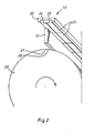
- An isometric view of part of the
exposure head 10 and the optical transer means 12 is shown in Fig. 2. The exposure head comprises an elongatechannel section bar 22 wherein a plurality ofexposure modules 23 are mounted next to each other. Each module comprises several arrays of emitters as will be explained further. The emitters of all the modules are arranged in twoparallel rows drum 20. - The optical transfer means 12 is an elongate element of plastic or the like wherein a plurality of self-focussing fibers are provided, the optical axis of the transfer means, or more correctly the optical plane thereof, passing through the axis of the drum.
- Due to the focussing power of the
element 12, each of the rows of emitters will be imaged on a respective transverse line on the photoreceptor, namely row 24 online 26, androw 25 online 27, both lines being represented by a dot on the figure. - A view of the
exposure head 10, from the optical transfer means towards the head, is represented in Fig. 3. A plurality ofmodules 23 are mounted next to each other in thebar 22 so that the total exposure length / corresponds with the desired width of the image on the photoreceptor. The direction of movement of the photoreceptor past the exposure head is indicated by the arrow 28. Thebar 22 is made of a metal whereby three important properties are united, namely a good heat conductivity, a good dimensional stability, and a good electric conductivity. The bar may optionally be provided with fins or the like for improving the heat transfer from the bar to the air. Suitable materials for the bar are e.g. brass, aluminium and copper. Themodules 23 are suitably secured in the bar by means of an electrically conductive quickly curing epoxy adhesive. The mounting of the exposure head in the apparatus may be arranged in such a way that slight adjustments of the positioning of the head are possible, thereby to ensure a true parallel alignment of theemitter rows - An enlarged view of one
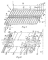
module 23 of the exposure head is illustrated in Fig. 4. Themodule 23 comprises ametal base plate 29 of brass, aluminium or the like, with a shape that deviates from a true rectangle by the presence of two slanting steps at the mid-width zone of the plate. These steps have been drawn in broken lines for thebase plate 29, and for the module at the right-hand side thereof, and infull line 30 for the module at the left-hand side ofmodule 23, the latter being shown in outline only, without its corresponding LED array. Fourarrays 31 of emitters are mounted on the base plate in abutting relationship. Each array has tworows chip arrays 31 is slightly greater than the length o of the base plate of the module, so that the first and fourth chip on each module extend over thesteps 30 of thebase plate 29 over a small distance in the order of magnitude of some tenths of a millimetre. Thereby it can be ensured that the end chips on the four modules are in firm contact with each other when the modules are assembled onbar 22. This is notably the case if a, + a2 = b as will be explained hereinafter. In those cases where a, + a2 < b, it will be understood that there is a spacing between the end edges of adjacent chips. The LED's of the several modules on the exposure head accordingly form two uninterrupted rows of LED's, these being uniformly spaced along the entire length of each row. For the sake of clarity, the right-hand LED array in Fig. 4 is shown spaced from the LED array on the neighbouring module. This separation will in practice be much smaller, in case a, + a2 < b, and this spacing will even be zero for a, + a2 = b. - The attachment of the
arrays 31 on thebase plates 29 is preferably also effected by means of an electrically conductive quickly curing epoxy adhesive. The electrical connections to the base chip material of each LED, in the present example the cathodes of the LED's are achieved via thebar 22. - The electric control means for the LED's are in the form of two
integrated circuits circuit 34 controlling the even LED's, i.e. the LED's ofrow 24, and thecircuit 35 controlling the odd LED's, i.e. those ofrow 25. Theintegrated circuits base plate 29. It will be understood that the mounting of the LED chips and the control chips on the base plates to form the modules, and the mounting of the modules on the barto produce the recording head, are carried out under a microscope in view of the minute dimensions of the components. A microscope is also needed for making the electrical connections between the control circuits and the LED's as will now be described with reference to Fig. 5. - Fig. 5 is a plan view of one
LED array 31. The 2 x 16 LED's are formed on achip substrate 36 in the form of a parallelogram. The substrate may have a length of approxiamately 2 mm and a width of 1 mm. The chip has been cut from a bar that itself has been cut from a circular slice with a diameter of about 5 cm onto which a great plurality of component arrays have been formed by means of monolithic integration techniques. Thechip 36 is actually a GaAs substrate that is provided at the lower side with a Au+ + Sn layer, and at the upper side with an epitaxially grown GaAsP (n-type) layer. In said upper layer there have been formed discrete Zn diffusion (p-type) areas. These are distributed in tworows strips 37 which at their inner ends haveopenings 38. These openings coincide with the sites of the mentioned Zn diffusion areas. Application of a suitable voltage to any of the electrodes causes a "LED" to be operative at the correspondingarea 38. The connection between each LED and the corresponding output of the control chip is formed byfinewires of gold that are applied according to the ball-and- stitch technique known in the art. The mentioned connections have been illustrated by thewires 39 for the connection of the upper row of LED's to thecorresponding output terminals 78 ofcontrol chip 34, and by thewires 79 for the connection of the lower row of LED's to theoutput terminals 77 ofcontrol chip 35. - The formation of rows of LED's that are uniformly spaced by assembling component arrays, is embodied in the illustrated apparatus in the following way, described with reference to Figs. 5 and 6.
- The
portions rows - The two
rows such edges - A second feature is that the sum of the distances a1 and a2 between the
ends row 24 may not be greater than the pitch b between two successive LED's, measured on thesame line 24. In the present embodiment a, = a2 and a, + a2 = b. - The result of the foregoing features is that uninterrupted rows of equally spaced LED's may be obtained if the LED arrays are mounted in such a way that the end edges of the successive chips abut against each other.
- The mounting of the modules on the bar in such a way that the end edges of the successive chips abut against each other puts not any problem since the end edges of the chips slightly protrude over the base plates of the modules, so that minor alterations of the position of a module while it is embedded in the adhesive on the bar can be easily carried out under the microscope, which yet the operator is not hindered by the relative position of the side edges of adjacent modules.
- Referring to the LED 44 (Fig. 6), it may be seen that the LED's active area has a hexagonal form, with the upper and
lower sides sides sides sides dot line 52. The described configuration of the LED's offers an adequate LED area, while yet allowing the portion of eachelectrode 37 that surrounds the active LED area to have a sufficient minimum width x, which minimum should in practice be not smaller than approximately 10 um to allow for manufacturing tolerances. The spacing of the LED's is such that they are not in projected image- touching relationship. Referring to Fig. 6, the projected spacing is indicated by m. It is clear that the spacing of the LED's may be such that the spacing m becomes zero, or that the projected images are even in overlapping relationship. - One of the integrated control circuits of one module, shown by the
chip 35 in Fig. 4 is illustrated in detail in Fig. 7. Theother control circuit 34 is the same. Inchip input terminal 74 and anoutput terminal 75, whereas 54 are load switches that are simultaneously controllable by aline 55, 56 is a latch register, 57 are individual drivers for each LED, and 58 is a line via which an adjustable bias voltage can be applied to set the current produced by thedrivers 57 in their operative condition. The outputs of thedrivers 57 are connected by means offine wires 39 to the corresponding LED's, L, to L63. All described elements of thechips 35, and thechip 34 that comprises the same elements for the controlling of the LED's L2 to L64, are integrated on a monolithic silicon chip. - The
output terminal 75 of theshift register 53 is connected to theinput terminal 74 of the shift register of the control chip of the module, etc., whereas the line 55 should be considered as controlling all the load switches of the control chips of all the modules. - The circuits for the control of the information flow to the recording head are illustrated dia- gramatically in Fig. 8, wherein 60 is a recording signal generator, 61 is a controller with an
input selector switch 62 that alternatively applies the input signal to the row of even and of odd LED's, 63 is an input memory selector with three positions a, b and c, 65, 66 and 67 are memories, 68 is an output memory selector with likewise three operative positions a, b and c. It will be understood that in practice the device will comprise many other circuits for the control of the different operations, such as a generator for a clock frequency, setting and re-setting circuits, synchronization circuits, etc. All these circuits are known in the art, and a description of them is not required for the understanding of the operation of the apparatus. - The
generator 60 produces an electric recording signal for the first image line to be recorded on the photoreceptor. Theswitch 62 is controlled by the clock frequency, e.g. a frequency of the order of magnitude of 3 MHz, such that the signal for the first image point of the first image line is put on line 70, the signal for the second image point is put in thememory 65 through switch position 63a, the signal for the third image point on line 70, the next one inmemory 65, and so on. The odd image signals that are fed to thecontrol chips 35 via line 70 are shifted successively through the shift registers of said chips, under the control of the clock signal online 72, until finally 1728 distinct image points have been read-in according to a serial-in mode. These are the odd image points. At the same time, 1728 even image points have been read-in in thememory 65. The total number of 3456 image points is determined by the recording head that comprises 27 modules with each four chips of 2 x 16 LED's. - An appropriate signal on line 55, see Fig. 7, causes the
switches 54 briefly to close, so that the signals for the odd image points in theregister 53 are now transferred according to a parallel-out mode to thelatch register 56, and this for eachmodule 23. The signals are stored in thelatch register 56 and the corresponding current is applied to the several LED's L1 through L63 for the first module, and to the LED's L1 through L3455 for the complete recording head. - When the photoreceptor has been advanced over a distance corresponding with the thickness of a recording line, the latch registers 56 are reset by an appropriate signal on
line 73, and signals for the second image line to be recorded are produced by thegenerator 60. - The second line signal. is now read-in, with the odd image points being again fed to the shift registers 53 of
control chips 35, whereas the even image points are, however, now fed to thememory 66 through selector position 63b. Theswitches 54 are closed, and the odd image points of the second image line are now recorded. - The third image line recording signal is then produced by the
generator 60, and the odd image points thereof are recorded as described already for the first and second lines. The even image points are stored in thememory 67 through selector position 63c. At the moment theswitch 63 was put in the position 63c,switch 68 was put in the position 68a, so that the even image point signals for the first image line, which were stored inmemory 65 are read out into the shift registers of the control chips 34 throughline 71, in synchronism with the reading-in of the odd signals of the third line into the shift registers of thechips 35. The delay of the recording of the even image points over two lines with respect to the recording of the odd image points compensates for the distance d (Fig. 6) between two rows of LED's, which distance is twice the distance between successive image lines on the photoreceptor. Otherwise said, it may be considered in reference to Fig. 2 thatline 26 is the first image line, whereasline 27 is already the third image line. - When the fourth image line recording signal is produced by the
generator 60, and the odd image point signals are directly recorded by being fed to thechips 35 via line 70, whereas the even image points are recorded through 63a in thememory 65 from which the even image point signals for the first image line have been removed in the meantime into the shift registers of thechips 34. The said direct recording of the odd fourth image line signals is accompanied by a simultaneous recording of the even second line signals read from thememory 66 through switch position 68b. - The recording of the fifth and the further image lines occurs according to the sequences described hereinbefore.
- The following data pertain to a particular embodiment of the invention as above described with reference to the drawings:
- Recording head:
- net recording length /: 216 mm
- number of LED's per row: 1728
- number of LED's per mm recording
- length: 16
- number of modules: 27
- number of LED's per chip: 2 x 16
- row spacing d = 125 µm
- LED spacing b: 125 pm
- staggering s: 62.5 pm
- angle of inclination a: 26.5650 angular degrees
- active LED area 43: 2250 11m2
- shift registers 53 and latch registers 56:
- 64 bits
- clock frequency: 3 Mhz
- optical transfer means: a Selfloc, type
SLA 20, manufactured by Nippon sheet glass Co., Ltd. - recording speed: 10 cm.s-1.
- The present invention is not limited to the above described embodiment.
- The chips with the radiation sources may have greater lengths than the illustrated
chips 31. For instance, the chips may have a length of approximately 8 mm, thereby to completely cover the base plate of a module, and also protrude at one side edge at least of the module. It will be understood that such longer chips may reduce the yield, since the number of defect-free LED arrays that may be obtained from a wafer decreases as the number of components per chip increases. - The control chips may comprise more than one shift register, and gate means for controlling the input arid outputs of said registers. In the mentioned way, a line signal may be clocked through several registers which in that may operate as memories for compensating the delay in the recording to two rows of image sources. This configuration would render the
memory circuits 65 through 67 illustrated in Fig. 8 superfluous. Alternatively, the control chips may comprise one shift register only for the serial-in and parallel-out processing of signals, and two or more parallel registers forthe successive parallel-out transfer of the signals in order to produce the desired delay over two or more line periods. - The angle a must not necessarily respond to the condition tga = s/d, although it appears that said condition permits to obtain a maximum ratio between the active LED area and the non-active LED area.
- The important portions of the end edges of the LED chips insofar as their orientation is concerned are the portions which cross the rows of LED's. Another example of a suitable LED chip shape is shown in Fig. 9. In this case the end edges of the chip have oblique medial portions crossing the LED rows and the end portions of those end edges are normal to those rows and to the longer edges of the chip. As a further example, such edges can be of stepped profile, the steps of one chip nesting into the steps of the next chip edge. Other shapings are also useful provided that the general or mean direction of the important portions of the end boundaries of the chips, that is the direction of a straight line that connects the two points of intersection of the chip end edge with the two rows of radiation sources, is oblique with respect to the rows of LED's.
- As an example of a module base plate shape other than that illustrated in Fig. 4, the base plates may be in the form of a parallelogram with the parallel edges of each base plate running parallel with the rows of LED's on the chips carried by the plates. The integrated circuits for the LED's may in such a case likewise have a parallelogram space form, better suited to that shape of base plate than the rectangular space form illustrated in Fig. 4.
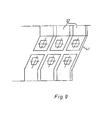
- The apparatus may also comprise a recording head wherein pairs of modules are provided, each module comprising one row only of radiation sources. Referring to Fig. 10 which is a diagrammatic plan view of a
recording head 90, anelongate bar 91 is provided with a plurality of pairs of modules such 92, 93 and 94, 95, mounted in side by side relationship to cover a recording width indicated by /, in a way similarly as described hereinbefore with reference to Fig. 3. The modules of each pair are identic, the modules of the lower row, such as 93 and 95 being turned over 180 angular degrees in their own plane with respect to theopposed modules chips - The lower modules such as 93 and 95 are slightly laterally shifted with respect to the upper modules such as 92 and 94, so that the LED's of the two
rows edge 102 of abase plate 95. It may even be considered to make the longitudinal edge of the chip extend beyond theedge 102 of the base plate of the module so that upon assembling of the head, the longitudinal edges of opposed chips may even touch each other while yet the corresponding longitudinal edges of the base plates of the modules have no contact. In the mentioned way, the same advantages are obtained as described already for the lateral edges of the base plates. - It will be appreciated that the yield of the described arrangement may be twice the yield of the recording head illustrated in Figs. 2 to 4. As a matter of fact, if the number of LED's per unit of length per row is equal, and the width of the modules is also equal, then it is clear that a module of the embodiment of Fig. 10 comprises only half the number of LED's of the embodiment of Figs. 2 to 4. The number of lost LED channels in the case of one defect channel on a module is thus 64 in the embodiment of Fig. 10, and 128 in the embodiment of Figs. 2 to 4.
- The LED's may have other structures than the GaAs disclosed in the example of the invention. Other structures are well known in the art and enable the LED's to radiate in other regions of the visible spectrum than in the red region, for instance in the green, yellow or blue region.
- As mentioned already in the introduction of the specification, the discrete radiation source function may also be performed by other types of active emitters, or by passive means such as light- valves that control the transmission of radiation from a suitable radiation source.
Claims (11)
Applications Claiming Priority (2)
| Application Number | Priority Date | Filing Date | Title |
|---|---|---|---|
| GB8205024 | 1982-02-19 | ||
| GB8205024 | 1982-02-19 |
Publications (3)
| Publication Number | Publication Date |
|---|---|
| EP0086907A2 EP0086907A2 (en) | 1983-08-31 |
| EP0086907A3 EP0086907A3 (en) | 1984-11-28 |
| EP0086907B1 true EP0086907B1 (en) | 1987-05-06 |
Family
ID=10528481
Family Applications (1)
| Application Number | Title | Priority Date | Filing Date |
|---|---|---|---|
| EP82201324A Expired EP0086907B1 (en) | 1982-02-19 | 1982-10-25 | Recording apparatus |
Country Status (5)
| Country | Link |
|---|---|
| US (1) | US4536778A (en) |
| EP (1) | EP0086907B1 (en) |
| JP (1) | JPS58142872A (en) |
| CA (1) | CA1203840A (en) |
| DE (1) | DE3276289D1 (en) |
Families Citing this family (53)
| Publication number | Priority date | Publication date | Assignee | Title |
|---|---|---|---|---|
| JPS58147386A (en) * | 1982-02-26 | 1983-09-02 | Canon Inc | Electronic apparatus with printer |
| EP0115088B1 (en) * | 1983-01-21 | 1986-12-30 | Agfa-Gevaert N.V. | Recording apparatus |
| JPS6027565A (en) * | 1983-07-25 | 1985-02-12 | Mitsubishi Electric Corp | Luminous diode array head and manufacture thereof |
| DE3438949C2 (en) * | 1983-10-25 | 1994-03-10 | Canon Kk | Printing device |
| DE3376727D1 (en) * | 1983-11-01 | 1988-06-23 | Agfa Gevaert Nv | Recording apparatus |
| JPH0825302B1 (en) * | 1984-09-27 | 1996-03-13 | Sanyo Denki Kk | |
| JPS61111061A (en) * | 1984-11-05 | 1986-05-29 | Casio Comput Co Ltd | Recorder |
| JPS61160982A (en) * | 1985-01-08 | 1986-07-21 | Mitsubishi Electric Corp | Led array head |
| US4589745A (en) * | 1985-01-25 | 1986-05-20 | Polaroid Corporation | Geometric LED layout for line exposure |
| JPS61211063A (en) * | 1985-03-15 | 1986-09-19 | Kyocera Corp | Optical printing head |
| EP0199852B1 (en) * | 1985-04-23 | 1990-08-29 | Agfa-Gevaert N.V. | Monolithic integration of light-emitting elements and driver electronics |
| EP0246481B1 (en) * | 1986-05-13 | 1990-12-27 | Heimann GmbH | Contact image sensor array |
| US4779108A (en) * | 1986-11-18 | 1988-10-18 | Sanyo Electric Co., Ltd. | Optical printer head |
| JP2816147B2 (en) * | 1987-03-27 | 1998-10-27 | 株式会社日立製作所 | Driver circuit for light emitting diode array |
| US4967192A (en) * | 1987-04-22 | 1990-10-30 | Hitachi, Ltd. | Light-emitting element array driver circuit |
| US4829321A (en) * | 1987-04-23 | 1989-05-09 | Hitachi Cable, Ltd. | Optical printer head with a light emitting diode array |
| US4799071A (en) * | 1987-09-21 | 1989-01-17 | Eastman Kodak Company | Dot printer with age compensation means |
| JPH0712712B2 (en) * | 1987-10-07 | 1995-02-15 | 双葉電子工業株式会社 | Fluorescent printer head |
| JPH059616Y2 (en) * | 1987-10-17 | 1993-03-10 | ||
| JP2630960B2 (en) * | 1987-10-17 | 1997-07-16 | グラフテック株式会社 | Waveform recording device using thermal dot array |
| US4912483A (en) * | 1987-10-22 | 1990-03-27 | Graphtec Kabushiki Kaisha | Balanced head suspension in thermal recorders |
| DE3808636A1 (en) * | 1988-03-15 | 1989-09-28 | Siemens Ag | CHARACTER GENERATOR FOR A NON-MECHANICAL PRINTER |
| US4927778A (en) * | 1988-08-05 | 1990-05-22 | Eastman Kodak Company | Method of improving yield of LED arrays |
| US4851862A (en) * | 1988-08-05 | 1989-07-25 | Eastman Kodak Company | Led array printhead with tab bonded wiring |
| US4821051A (en) * | 1988-09-01 | 1989-04-11 | Eastman Kodak Company | Optical printhead having thermal expansion stress relief |
| US4913526A (en) * | 1988-09-01 | 1990-04-03 | Eastman Kodak Company | Optical LED printhead with lens locator bar |
| US5014074A (en) * | 1988-10-11 | 1991-05-07 | Hewlett-Packard Company | Light emitting diode print head assembly |
| US4942405A (en) * | 1988-10-11 | 1990-07-17 | Hewlett-Packard Company | Light emitting diode print head assembly |
| JP2845933B2 (en) * | 1989-04-24 | 1999-01-13 | キヤノン株式会社 | Recording head unit |
| NL8901230A (en) * | 1989-05-17 | 1990-12-17 | Oce Nederland Bv | EXPOSURE AND PRINTING DEVICE. |
| US5317344A (en) * | 1989-12-22 | 1994-05-31 | Eastman Kodak Company | Light emitting diode printhead having improved signal distribution apparatus |
| US5543830A (en) * | 1990-10-12 | 1996-08-06 | Minnesota Mining And Manufacturing Company | Apparatus with light emitting element, microlens and gradient index lens characteristics for imaging continuous tone images |
| DE69211881T2 (en) * | 1991-04-04 | 1997-02-06 | Agfa Gevaert Nv | LED exposure head |
| US5818500A (en) * | 1991-05-06 | 1998-10-06 | Eastman Kodak Company | High resolution field emission image source and image recording apparatus |
| US5872587A (en) * | 1991-07-16 | 1999-02-16 | Minolta Co., Ltd. | Light signal generating device with reduced light leakage |
| JP2937577B2 (en) * | 1991-09-11 | 1999-08-23 | 双葉電子工業 株式会社 | Light source for fluorescent printer |
| NL9101745A (en) * | 1991-10-18 | 1993-05-17 | Oce Nederland Bv | EXPOSURE AND PRINTING DEVICE. |
| CA2077813C (en) * | 1991-12-20 | 1998-07-28 | Thomas L. Paoli | Apparatus and method for spot position control in an output device employing a linear array of light sources |
| US5606358A (en) * | 1991-12-23 | 1997-02-25 | Eastman Kodak Company | Light-emitting diode printhead |
| DE4303225C2 (en) * | 1993-02-04 | 1996-08-14 | Siemens Nixdorf Inf Syst | Optical character generator for an electrographic printer |
| DE4308864C2 (en) * | 1992-06-25 | 1996-05-09 | Agfa Gevaert Ag | Device for copying transparent image templates |
| US5640188A (en) * | 1992-12-18 | 1997-06-17 | Xerox Corporation | Multiple diode laser employing mating substrates |
| JP2845719B2 (en) * | 1993-04-12 | 1999-01-13 | 沖電気工業株式会社 | Driver IC |
| EP0629507B1 (en) * | 1993-06-18 | 1997-12-03 | Xeikon Nv | Led recording head |
| NL9301330A (en) * | 1993-07-30 | 1995-02-16 | Oce Nederland Bv | Print device equipped with an LED array. |
| US5764273A (en) * | 1993-08-27 | 1998-06-09 | Xerox Corporation | Spot position control using a linear array of light valves |
| US5638108A (en) * | 1994-08-31 | 1997-06-10 | Xerox Corporation | Lower resolution led bars used for 600 SPI printing |
| JP3185204B2 (en) * | 1995-05-31 | 2001-07-09 | 日本精機株式会社 | Light emitting device assembly |
| JP3227385B2 (en) * | 1996-07-11 | 2001-11-12 | キヤノン株式会社 | Image forming device |
| US7151557B2 (en) * | 2004-03-19 | 2006-12-19 | Lexmark International, Inc. | Collimation assembly for adjusting laser light sources in a multi-beamed laser scanning unit |
| US8096634B2 (en) * | 2007-09-17 | 2012-01-17 | Xerox Corporation | Temperature compensation for full-width arrays write heads |
| GB201209142D0 (en) * | 2012-05-24 | 2012-07-04 | Lumejet Holdings Ltd | Media exposure device |
| JP6156402B2 (en) * | 2015-02-13 | 2017-07-05 | 日亜化学工業株式会社 | Light emitting device |
Family Cites Families (11)
| Publication number | Priority date | Publication date | Assignee | Title |
|---|---|---|---|---|
| FR2178433A5 (en) * | 1972-03-31 | 1973-11-09 | Radiotechnique Compelec | |
| US3952311A (en) * | 1972-04-24 | 1976-04-20 | The Laitram Corporation | Electro-optical printing system |
| US4455562A (en) * | 1981-08-14 | 1984-06-19 | Pitney Bowes Inc. | Control of a light emitting diode array |
| EP0022704B1 (en) * | 1979-07-13 | 1983-12-14 | COMPAGNIE INDUSTRIELLE DES TELECOMMUNICATIONS CIT-ALCATEL S.A. dite: | Image printing array, its manufacturing method and image printing device |
| JPS5630154A (en) * | 1979-08-21 | 1981-03-26 | Oki Electric Ind Co Ltd | Photoprint head |
| JPS5710162A (en) * | 1980-06-23 | 1982-01-19 | Nippon Telegr & Teleph Corp <Ntt> | Exposure system of electrophotography |
| CA1175884A (en) * | 1980-06-25 | 1984-10-09 | Hugh St. L. Dannatt | Light emitting diode assembly |
| WO1982004353A1 (en) * | 1981-05-26 | 1982-12-09 | Haydn Victor Purdy | Light emitting diode array devices and image transfer systems |
| US4413269A (en) * | 1981-11-23 | 1983-11-01 | International Business Machines Corporation | Method of and apparatus for controlling gray scale while printing on charge sensitive recording mediums |
| US4427275A (en) * | 1982-07-22 | 1984-01-24 | Pitney Bowes Inc. | Xerographic electronic printer |
| US4455578A (en) * | 1982-08-30 | 1984-06-19 | Eastman Kodak Company | Electronics for arrayed photosources |
-
1982
- 1982-10-25 EP EP82201324A patent/EP0086907B1/en not_active Expired
- 1982-10-25 DE DE8282201324T patent/DE3276289D1/en not_active Expired
- 1982-10-26 US US06/436,671 patent/US4536778A/en not_active Expired - Fee Related
- 1982-11-04 JP JP57194479A patent/JPS58142872A/en active Granted
- 1982-11-05 CA CA000415021A patent/CA1203840A/en not_active Expired
Also Published As
| Publication number | Publication date |
|---|---|
| EP0086907A3 (en) | 1984-11-28 |
| JPH0342188B2 (en) | 1991-06-26 |
| JPS58142872A (en) | 1983-08-25 |
| CA1203840A (en) | 1986-04-29 |
| US4536778A (en) | 1985-08-20 |
| DE3276289D1 (en) | 1987-06-11 |
| EP0086907A2 (en) | 1983-08-31 |
Similar Documents
| Publication | Publication Date | Title |
|---|---|---|
| EP0086907B1 (en) | Recording apparatus | |
| EP0115088B1 (en) | Recording apparatus | |
| EP0141880B1 (en) | Recording apparatus | |
| EP0460194B1 (en) | A light emitting diode printhead having improved signal distribution apparatus | |
| EP0098382B1 (en) | Uniformly intense imaging by close-packed lens array | |
| EP0786353B1 (en) | Led printing head | |
| CA1230637A (en) | Recording apparatus | |
| US5323084A (en) | Light emitting diode printhead | |
| US5274401A (en) | Electrostatic printhead | |
| EP0247699B1 (en) | Image-forming element for an electrostatic printer, and a printer in which an element of this kind is used | |
| US4318597A (en) | Optical print head for optical printing devices | |
| CA1238941A (en) | Geometric led layout for line exposure | |
| GB2099221A (en) | Light emitting diode array devices and image transfer systems | |
| EP0464948B1 (en) | LED exposure head with overlapping electric circuits. | |
| JP2001130051A (en) | Exposure device and image forming apparatus | |
| WO1982004353A1 (en) | Light emitting diode array devices and image transfer systems | |
| JP2991259B2 (en) | Image forming device | |
| JPH03231478A (en) | Array of light-emitting element or photodetector, apparatus for photographic printing or reading using the array, and manufacture of the array | |
| JP2000174986A (en) | Exposure device and image forming device using the same | |
| JPH08192534A (en) | Led printing head | |
| JPH10157194A (en) | Optical print head | |
| JPH11188918A (en) | Image forming apparatus | |
| JPH06334221A (en) | Imaging device |
Legal Events
| Date | Code | Title | Description |
|---|---|---|---|
| PUAI | Public reference made under article 153(3) epc to a published international application that has entered the european phase |
Free format text: ORIGINAL CODE: 0009012 |
|
| AK | Designated contracting states |
Designated state(s): BE DE FR GB IT NL |
|
| PUAL | Search report despatched |
Free format text: ORIGINAL CODE: 0009013 |
|
| AK | Designated contracting states |
Designated state(s): BE DE FR GB IT NL |
|
| 17P | Request for examination filed |
Effective date: 19850406 |
|
| 17Q | First examination report despatched |
Effective date: 19860424 |
|
| GRAA | (expected) grant |
Free format text: ORIGINAL CODE: 0009210 |
|
| AK | Designated contracting states |
Kind code of ref document: B1 Designated state(s): BE DE FR GB IT NL |
|
| REF | Corresponds to: |
Ref document number: 3276289 Country of ref document: DE Date of ref document: 19870611 |
|
| ITF | It: translation for a ep patent filed |
Owner name: AGFA-GEVAERT S.P.A |
|
| ET | Fr: translation filed | ||
| PLBE | No opposition filed within time limit |
Free format text: ORIGINAL CODE: 0009261 |
|
| STAA | Information on the status of an ep patent application or granted ep patent |
Free format text: STATUS: NO OPPOSITION FILED WITHIN TIME LIMIT |
|
| 26N | No opposition filed | ||
| ITTA | It: last paid annual fee | ||
| PGFP | Annual fee paid to national office [announced via postgrant information from national office to epo] |
Ref country code: BE Payment date: 19950821 Year of fee payment: 14 |
|
| PGFP | Annual fee paid to national office [announced via postgrant information from national office to epo] |
Ref country code: NL Payment date: 19951019 Year of fee payment: 14 |
|
| PG25 | Lapsed in a contracting state [announced via postgrant information from national office to epo] |
Ref country code: BE Effective date: 19961031 |
|
| REG | Reference to a national code |
Ref country code: GB Ref legal event code: 746 Effective date: 19961118 |
|
| REG | Reference to a national code |
Ref country code: FR Ref legal event code: D6 |
|
| BERE | Be: lapsed |
Owner name: AGFA-GEVAERT N.V. Effective date: 19961031 |
|
| PG25 | Lapsed in a contracting state [announced via postgrant information from national office to epo] |
Ref country code: NL Effective date: 19970501 |
|
| NLV4 | Nl: lapsed or anulled due to non-payment of the annual fee |
Effective date: 19970501 |
|
| PGFP | Annual fee paid to national office [announced via postgrant information from national office to epo] |
Ref country code: GB Payment date: 19980810 Year of fee payment: 17 |
|
| PGFP | Annual fee paid to national office [announced via postgrant information from national office to epo] |
Ref country code: FR Payment date: 19980922 Year of fee payment: 17 |
|
| PG25 | Lapsed in a contracting state [announced via postgrant information from national office to epo] |
Ref country code: GB Free format text: LAPSE BECAUSE OF NON-PAYMENT OF DUE FEES Effective date: 19991025 |
|
| GBPC | Gb: european patent ceased through non-payment of renewal fee |
Effective date: 19991025 |
|
| PG25 | Lapsed in a contracting state [announced via postgrant information from national office to epo] |
Ref country code: FR Free format text: LAPSE BECAUSE OF NON-PAYMENT OF DUE FEES Effective date: 20000630 |
|
| REG | Reference to a national code |
Ref country code: FR Ref legal event code: ST |
|
| PGFP | Annual fee paid to national office [announced via postgrant information from national office to epo] |
Ref country code: DE Payment date: 20010829 Year of fee payment: 20 |