EP0106550A2 - Method of driving a matrix type display - Google Patents
Method of driving a matrix type display Download PDFInfo
- Publication number
- EP0106550A2 EP0106550A2 EP83305504A EP83305504A EP0106550A2 EP 0106550 A2 EP0106550 A2 EP 0106550A2 EP 83305504 A EP83305504 A EP 83305504A EP 83305504 A EP83305504 A EP 83305504A EP 0106550 A2 EP0106550 A2 EP 0106550A2
- Authority
- EP
- European Patent Office
- Prior art keywords
- electrodes
- data
- scanning
- voltage
- display
- Prior art date
- Legal status (The legal status is an assumption and is not a legal conclusion. Google has not performed a legal analysis and makes no representation as to the accuracy of the status listed.)
- Granted
Links
Images


Classifications
-
- G—PHYSICS
- G09—EDUCATION; CRYPTOGRAPHY; DISPLAY; ADVERTISING; SEALS
- G09G—ARRANGEMENTS OR CIRCUITS FOR CONTROL OF INDICATING DEVICES USING STATIC MEANS TO PRESENT VARIABLE INFORMATION
- G09G3/00—Control arrangements or circuits, of interest only in connection with visual indicators other than cathode-ray tubes
- G09G3/20—Control arrangements or circuits, of interest only in connection with visual indicators other than cathode-ray tubes for presentation of an assembly of a number of characters, e.g. a page, by composing the assembly by combination of individual elements arranged in a matrix no fixed position being assigned to or needed to be assigned to the individual characters or partial characters
- G09G3/22—Control arrangements or circuits, of interest only in connection with visual indicators other than cathode-ray tubes for presentation of an assembly of a number of characters, e.g. a page, by composing the assembly by combination of individual elements arranged in a matrix no fixed position being assigned to or needed to be assigned to the individual characters or partial characters using controlled light sources
- G09G3/30—Control arrangements or circuits, of interest only in connection with visual indicators other than cathode-ray tubes for presentation of an assembly of a number of characters, e.g. a page, by composing the assembly by combination of individual elements arranged in a matrix no fixed position being assigned to or needed to be assigned to the individual characters or partial characters using controlled light sources using electroluminescent panels
-
- G—PHYSICS
- G09—EDUCATION; CRYPTOGRAPHY; DISPLAY; ADVERTISING; SEALS
- G09G—ARRANGEMENTS OR CIRCUITS FOR CONTROL OF INDICATING DEVICES USING STATIC MEANS TO PRESENT VARIABLE INFORMATION
- G09G2310/00—Command of the display device
- G09G2310/02—Addressing, scanning or driving the display screen or processing steps related thereto
- G09G2310/0264—Details of driving circuits
- G09G2310/0267—Details of drivers for scan electrodes, other than drivers for liquid crystal, plasma or OLED displays
-
- G—PHYSICS
- G09—EDUCATION; CRYPTOGRAPHY; DISPLAY; ADVERTISING; SEALS
- G09G—ARRANGEMENTS OR CIRCUITS FOR CONTROL OF INDICATING DEVICES USING STATIC MEANS TO PRESENT VARIABLE INFORMATION
- G09G2310/00—Command of the display device
- G09G2310/02—Addressing, scanning or driving the display screen or processing steps related thereto
- G09G2310/0264—Details of driving circuits
- G09G2310/0275—Details of drivers for data electrodes, other than drivers for liquid crystal, plasma or OLED displays, not related to handling digital grey scale data or to communication of data to the pixels by means of a current
-
- G—PHYSICS
- G09—EDUCATION; CRYPTOGRAPHY; DISPLAY; ADVERTISING; SEALS
- G09G—ARRANGEMENTS OR CIRCUITS FOR CONTROL OF INDICATING DEVICES USING STATIC MEANS TO PRESENT VARIABLE INFORMATION
- G09G2320/00—Control of display operating conditions
- G09G2320/02—Improving the quality of display appearance
- G09G2320/0223—Compensation for problems related to R-C delay and attenuation in electrodes of matrix panels, e.g. in gate electrodes or on-substrate video signal electrodes
Definitions
- the present invention relates to a method of driving a matrix type display panel.
- One matrix type display device in which capacitive display cells are arranged in the form of matrix, is a display panel having a structure wherein scanning electrodes and data electrodes orthogonal thereto are arranged on insulating layers on opposite sides of a display medium such as an EL (electro luminescence) material or a discharge gas.
- a display medium such as an EL (electro luminescence) material or a discharge gas.
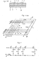
- an AC driven type thin film EL display panel has been proposed having a multi-layer thin film structure as shown in Fig. 1(A) of the accompanying drawings, which is a partial sectional view of the panel.
- the panel 10 has a structure in which translucent data electrodes 2 are provided on a translucent glass substrate 1, an EL layer 4, such as Zn S:Mn, is sandwiched between insulation layers 3 and 5, and metal scanning electrodes 6, for example Al electodes, are provided on the upper insulation layer 5.
- the data electrodes 2 and scanning electrodes 6 are arranged mutually orthogonally to form a matrix in which display cells 7 are defined each at a location where opposed electrodes cross.
- a selected display cell is caused to light upon receipt of a combined voltage resulting from a scanning pulse and a data pulse selectively applied to the two electrodes defining the cell.
- a refresh drive method is employed in which the panel is first address- scanned on a line at a time basis by such selection pulses and then the addressed points or cells are caused to emit light again by applying in common refresh pulses of polarity opposite to the selection pulses.
- the resistance of the translucent electrodes 2 on the substrate side, used in the above panel as data electrodes 2 is inevitably higher than the resistance of the metal scanning electrodes 6.
- a translucent electrode is formed, for example, as a mixed vacuum-deposited film of tin oxide and indium oxide (ITO), and such a translucent electrode has a comparatively high resistance.
- An electrode resistance of about 20 k ⁇ is experienced with an electrode length of 200 mm in a display panel of 1000 x 1000 cells with five electrodes per 1 mm of a width of 0.15 mm.
- Figures 1(B),2 and 3 relate to case in which a display cell group associated with a data electrode D 1 is selected for light emission.
- 1 is a substrate
- D 1 ⁇ D 1000 are translucent data electrodes
- S 1 ⁇ S 1000 are metal scanning electrodes
- S n is a display cell along data electrode D 1 nearest to the data power supply (hereinafter referred to as the nearest cell within the panel)
- S f is a display cell furthest from the data power supply along D 1 (hereinafter referred to as the furthest cell within the panel).
- rd is the resistance value of data electrode D 1 per cell
- CS is cell capacitance
- panel electrode resistance and panel cell capacitance as seen from the driving end of data electrode D 1 , form a CR ladder circuit and there is a great difference between the CR time constants nearer to and further from the data power supply driving end.
- data voltage pulses DP as shown in Figure 3 (a) supplied from the dat.a power supply to the data electrode D 1 as half-selection voltages are applied with a waveform as shown in Figure 3 f (b) nearer to the data power supply , but are applied with a waveform as shown in Figure 3(c), in which the pulse rising edges are dulled, to more remote cells.
- the voltage waveforms (g) and (h) are the results of the combinations of data voltage pulses applied to the data electrode D 1 and scanning voltage pulses applied to the scanning electrodes S 1 and S 1000 as shown in waveforms (d) and (f) of Figure 3.
- a particular problem occurs in that the furthest cell S f may not have a sufficient voltage applied to cause it to emit light and therefore brightness is less than at the nearest cell S n and accordingly the brightness varies over the matrix of display cells.
- the output.terminals of alternate transparent electrodes may be at opposite edges of the panel, and connected to drivers. Therefore, cells nearest to drivers and cells-farthest from the drivers occur alternately along a line at one of those edges of the panel and brightness nonumiformity between display cells is obvious.
- Electrode length and size are different, similar problems also occur even when the same electrode material is used for all electrodes (for example, a longer electrode has a high electrode resistance).
- a method for driving a matrix display panel which provides the scanning electrodes and data electrodes mutually having different resistance values and obtains electro-optical display effect through application of voltage of the specified level to the display cells defined at the intersecting points of said both electrode from both electrodes, characterised in that a selection : voltage, which gives electro-optical display effect to the selected display cells, is applied in such a form as having the two stages of rising waveform consisting of the first rising part which rises preceding a sufficient time for alleviating influence of larger electrode resistance and the second rising part which is combined on said first part and gives the effect a full selection.
- a method for driving an EL display panel which obtains electro-optical display effect by applying voltage of the specified level to the display cells defined at the intersecting points of the scanning electrodes and data electrodes from both electrodes,.wherein, on the occasion of giving electro-optical display effect to the selected display cells, a voltage to be applied to the electrode having higher resistance among the data electrode and scanning electrode forming the selected-display cells is applied preceding the voltage to be applied to the electrode having a lower electrode resistance.
- a method for driving an EL display panel which provides the light emitting layer and the scanning electrodes and data electrodes in the matrix arrangement capacitively coupled to said light emitting layer and obtains light emission for display by applying the selection pulse voltage in the specified level from both electrodes to the display cells defined at the intersecting points of both electrodes, wherein , on the occasion that electrode resistance of said scanning electrodes is different from said data electrodes, the selection pulse supplied from the higher resistance electrodes rises preceding the selection pulse supplied from the lower resistance electrodes, and the non-selected electrodes in the lower resistance electrodes'are maintained in the floating condition during such period.
- a method for driving a matrix display panel providing a display medium layer and the scanning electrodes and data electrodes in the matrix arrangement coupled capacitively to said display medium layer and obtaining electro-optical display effect by applying the display voltage of the specified level from both electrodes to the display cells defined at the intersecting points of these electrodes, wherein said scanning electrode is provided with a scanning driver for sequentially and selectively connecting each electrode to the reference voltage; said data electrode is provided with the first means which gives a bias voltage in common to plurality of data electrodes and the second means which gives thereto a voltage in accordance with light emission or no emission of display cells; and the voltage given to the data electrode means from the first or second means rises preceding the other means in accordance with either electrode having a higher resistance among the scanning and data electrodes.
- An embodiment of this invention can provide a method of driving a matrix display panel. having. electrodes with different resistance values by which variations in brightness of emitted light are reduced.
- An embodiment.of this invention can provide a method of driving a large scale matrix display panel giving a distinctivie display with uniform brightness over the entire display surface.
- An embodiment of this invention can provide a method for driving capacitive display cells which can reduce power consumption required for selective operation of many display cells.
- the present invention concerns a display panel in which capacitive display cells are arranged in the form of matrix, and more specifically provides a method of driving such a display panel, for example a thin film EL display device , in such a manner that variation of brightness of emitted light caused by the effects of electrode resistance can be reduced.
- an embodiment of this invention provides that a selection voltage, applied to selected display cells of a matrix display panel having data electrodes and scanning electrodes.respectively of different resistance values, to obtain an electro-optical display effect at the selected display cells, is applied with a two-stage rising waveform comprising a first part which rises sufficiently early to alleviate the effects of electrode resistance of the electrodes having the larger resistance value and.a second part which is combined with (superimposed on) the first part and gives a full selection effect.
- a combined voltage waveform to be applied to a furthest cell within the panel at a full selection time is sharp and is almost the same as the combined voltage waveform applied at that time in the nearest cell within the panel. Therefore, difference in display brightness between those cells can be substantially eliminated.
- An embodiment of the present invention further provides that when addressing is carried out continuously to adjacent display cells on the same data electrode, a data pulse for that same data electrode is effectively supplied continuously whilst the plurality of scanning electrodes, related to the pertinent adjacent display cells are scanned. Thereby, unwanted power consumption which would be caused by the intermittent application of data pulses when continuously addressing adjacent display cells can be reduced. Accordingly, since the data pulse is applied precedingly, fluctuation of brightness as a result of the influence of electrode resistance on the data electrode side can also be eliminated.
- the driving voltage waveforms of Figure 4 relate to a case in which a display cell group associated with a translucent data electrode D 1 is caused selectively to emit light, as in the case of the driving voltage waveforms of Figure 3.
- a data voltage pulse DP as shown in Figure 4 to be applied as a half selection voltage to a display cell group along selected data electrodes, has a waveform having a pulse width such that it is applied during one display line address (write) period (16 ⁇ sec, for example) to realize quicker rising (to provide earlier rising) than a scanning voltage pulse SP applied as a half selection voltage to the display cell group along the relevant scanning electrodes.
- a data voltage pulse DP is applied to a data electrode 8 ⁇ sec in advance of the rising of a scanning voltage pulse SP.
- a data voltage pulse as applied to the data electrode of the furthest -cell S f within the panel has a rising edge which dulled, as shown in Figure 4(c), but in the case of Figure 4 nevertheless reaches a specified voltage at the proper time of full selection when a scanning voltage pulse is applied to the corresponding scanning electrode S 1000 .
- a voltage pulse PS f applied to the furthest cell S f within the panel has a rising waveform which rises in two stages ; a first corresponding to rising of the data voltage DP in advance of the scanning voltage, and a second corresponding to superimposition of the scanning voltage SP on the data voltage DP.
- the voltage pulse PS f is thus provided with a waveform similar to that of voltage pulse PS n applied to the nearest cell S within the panel , as shown in Figure 4(g), at the time of full selection. Therefore, brightness at the pertinent furthest cell S f is no longer reduced by electrode resistance and there is little difference in brightness between nearest and furthest cells within the panel.
- TA is an address period
- TS is a refresh period. During the refresh period, an address pulse and a refresh pulse RP of reverse polarity are simultaneously applied to all display cells.
- the data voltage pulse providing .the first part of pulse PS f has a pulse width corresponding to one cell address time and therefore rises considerably in advance of the scanning voltage pulse providing the second part.
- the rise time of a data pulse can also be set a little slow (e.g.. can be later than shown in Figure 4) in accordance with the size and characteristics of the panel, because it is enough if the data pulse rises sufficiently early to mitigate the influence of electrode resistance on the translucent data electrode side.
- switching of a data driver can conveniently be omitted when obtaining continuous light emission from adjacent display cells on the same data electrode.
- FIG. 5 is a schematic block diagram of an EL panel drive circuit providing panel driving as explained with reference to Figure 4.
- Y side metal scanning electrodes S 1 ⁇ S 1000 of a thin film EL display panel 10 are connected with scanning drivers Q S1 ⁇ Q S1000 from which are sequentially driven by scanning signals sent from a scanning shift register 11 and which are connected to a scanning voltage -Y Na .
- X side translucent data electrodes D 1 ⁇ D 1000 extending vertically of the display panel 10 in Figure 5 are connected with data drivers Q d1 ⁇ Q d1000 and are connected to an address voltage V a .
- Data drivers corresponding to data electrodes are driven in parallel on a line at a time basis using signals sent from a latch circuit 13 which temporarily stores a parallel address signal sent from a shift register 12 for holding a data address. For example, when a scanning electrode line. is scanned, data drivers of data electrodes corresponding to..all the cells along the scanning electrode which are to be caused to emit light are driven in parallel. This takes place for each scanning electrode line, one line at a time.
- the latch circuit 13 for storing the parallel address signal is provided in the address circuitry on the data electrode side and therefore an address signal for the data drivers can be maintained in. the same condition so long as there is no change in the address signal (i.e. so long as the address signal for a next scanning electrode line does not differ from that of a present scanning line)... This-is so even when it is necessary for time to be taken to input and output. series address signals to and from the shift register 12 for each scanning line. That is, although the shift register 12 may be loaded and unloaded for each scanning line, the latch circuit 13 can provide an unchanging output.
- the latch circuit 13 provides, for example, a flip-flop corresponding to each data driver the output condition of each flip-flop being changed in accordance with address data being set in bits of the shift register 12.
- the contents of the bit of the shift register 12 corresponding to those cells is the same for all the relevant adjacent scanning lines and the corresponding output of the latch circuit 13 does not change and the corresponding data driver can be driven continuously.
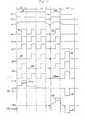
- Figure 6 shows driving voltage waveforms pertinent to this embodiment.
- Figure 6(a) is a datapulseDP output voltage waveform as supplied to a selected translucent data electrode from a data driver;
- (b) is data pulse waveform as supplied to the nearest cell Sn connected to the data driver
- (c) is data pulse waveform as supplied to the furthest cell S f connected to the driver ;
- (d) ⁇ (f) are waveforms of scanning pulses SP as supplied to scanning electrodes . from scanning drivers ;
- (g) is a combined voltage waveform as supplied to the nearest cell S n and giving an address pulse PS ;
- (h) is a combined voltage waveform as supplied to the furthest cell S f and giving an address pulse PS f .
- non-selected scanning electrodes are clamped to ground potential while-cells are being addressed to establish a display as explained above, unwanted charging current flows into cells along non-selected scanning electrodes during the early rise of data pulses DP and power is consumed uselessly. It is convenient, to prevent such useless flow of charging current, to keep non-selected scanning electrodes in a floating condition to give them a high impedance.
- broken lines indicate floating voltages and the potential.of non-selected scanning electrodes is floated in accordance with the selection condition of opposing data electrodes.
- the data electrodes have higher resistance than the scanning electrodes and the early rising pulses are applie.dto the data electrodes.
- the scanning pulses are caused to rise earlier than data pulses on the data electrodes in other embodiments of the present invention.
- a selection operation is carried out by applying positive and negative half-selecting voltage pulses from both data and scanning electrode sides.
- the relative selection voltage levels applied to the data and scanning electrodes can be set freely consistent with a range of values in which the combined voltage effective.at a selected cell is capable of giving a full selection effect.
- Figure 7 shows a drive circuit for an EL display panel in accordance with another embodiment of the present invention.
- a line driver DO on the data side comprises driving transistors Q 1 , Q 2 paired in correspondence to data electrodes D 1 ⁇ D 1000 and having respective input terminal pairs (a 1 , a 1 ),(a 2 , a 2 ) .... to which reverse data is applied (the terminals of a pair receive complementary data values).
- a line driver SD on the scanning side has scanning transistors Q 3 corresponding to respective scanning electrodes S 1 ⁇ S 1000 .
- the scanning transistors Q 3 have input terminals b 1 , b 2 ... which receive scanning data and the transistors are sequentially driven into an ON condition, connecting the corresponding scanning electrodes S 1 , S 2 ... to earth potential in sequence.
- Not-selected scanning electrodes are maintained in a floating condition since the scanning transistors Q 3 of these electrodes are in an OFF state.
- a bias pulse (a bias pedestal pulse PP) of voltage V p is supplied (to the data electrodes) from a bias source PS through a first power supply line l 1 for each selection of a scanning electrode S 1 ,S 2 , ... and display data corresponding to the scanning electrodes S 1 , S 2 , ... selected by control equipment (not shown) is applied t Q the input terminals (a 1 , a 1 ), ( a 2 , a 2 ) ,....
- P channel MOS transistors Q 1 are set to an "ON” state and N channel MOS transistors Q2 are set to an "OFF” state by applying low level signals to both input terminals a 1 , a 2 ... and a 1 , a 2 ... at the same time.
- transistors Q 1 and Q 2 are set to "OFF" and "ON" states respectively, by applying high level signals to said input terminals.
- data pulses DP of a voltage V D are supplied to data electrodes D 1 ,D 2 , ... which correspond to cells required to emit light through a second power line l 2 from a data power supply DS superimposed on the bias pedestal pulse PP.
- display panel DISP.in Figure 7
- display cells at the crossing points of selected scanning electrodes namely the scanning electrodes connected..to the earth potential, and the data electrodes to which the data pulses DP are applied (superimposed on pulse PP) emit light.
- Such operations are sequentially carried out for the scanning electrodes S 1 , S 2 , ... and when a final scanning electrode S 1000 is selected and driven, a refresh pulse RP is applied to all display cells from a refresh power source RS connected in common to the scanning electrodes.
- a refresh pulse RP is applied to all display cells from a refresh power source RS connected in common to the scanning electrodes.
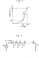
- the general light emitting characteristics of an EL display panel are shown in the graph of Figure 8. Only a low brightness level LD can be obtained when a bias pulse PP is applied alone and this is virtually undetectable visually. Meanwhile, when a data pulse DP is superimposed on a bias pulse PP, a high brightness level LS can be obtained, resulting in bright display effect.
- the data electrodes D 1 ⁇ D 1000 are formed of translucent conductive film and their electrode .resistance is high, load as viewed from a line data driver and load as viewed from a bias power source become heavy .
- the load viewed from the line data driver is a ladder type circuit RC circuit consisting of panel electrode resistances rd and panel cell capacitances C S . as in the case of the equivalent circuit of Figure 2 mentioned above. Therefore, there is a large difference in CR time constant, as viewed from the driver, between the nearer and further portions of an electrode.
- a CR time constant at a furthest cell as viewed from the line data driver can be expressed as 1000 2 rd C S /2, whilst a CR time constant of the furthest cell as viewed. from the bias power source can be expressed as 1000 rd. CS.
- a data pulse DP as shown at Figure 10(a), supplied to a data electrode D 1 from a line data driver, and a bias pulse PP as shown at 10(d), supplied from a bias power supply are applied as pulses having almost identical rising profiles, as seen at 10(b) and 1Q(e), at electrode portions nearer to the driver and power supply, but are applied as pulses of which only the rising edge of the data pulse DP is significantly dulled, as seen in 10(c) and 10(f), at furthest electrode portions.
- the light emitting voltages at S n and Sf are provided by combination of scanning voltage pulses SP 1 , SP 1000 as applied to scanning electrodes S 1 and 5 1000 , as shown in Figures 10(g) and 10(i), with 10(c) and 10(f).
- the furthest cell S f may not receive a voltage sufficient to cause light emission and this gives it a brightness lower than that of the nearest cell S n .
- the disadvantage that the brightness varies between display cells occurs in the case of Figure 10 as in the case of Figure 3.
- Figure 11 shows the driving voltage waveforms used in such an embodiment of the present invention. It will be seen that-voltage pulse waveforms output from a line data driver DD as shown in Figure 11 differ significantly from those of Figure 10. Namely, a data voltage pulse DP as shown. in Figure 11 ( Figure 11(a) ) has a waveform having a pulse width so that it is applied during the address (write) period (16 ⁇ sec, for example) of one display line in order that if it rises more quickly than a bias pulse PP. More concretely, such data pulse DP is applied to the data electrode 8 ⁇ sec in advance of the rise of bias pulse PP.
- a data pulse as applied to the data electrode of the furthest cell S f within the panel has a dulled rising edge as shown in Figure 11(c), but a predetermined light emitting voltage is reached when the bias pulse PP is applied, under the condition that the scanning voltage pulse SP 1000 is applied to the corresponding scanning electrode S 1000 , namely earth voltage is applied. Therefore, the voltage pulse PS f applied to the furthest cell S f within the panel becomes, as shown in Figure 11(k), almost the same as the voltage pulse PS n applied to the nearest cell S n within the panel shown in Figure 11(j) and the pertinent furthest cell S f can emit light in an optimum condition, namely of a high brightness. Thereby, there is little difference between the brightness of light emitted by the nearest cell and that emitted by the furthest cell within the panel.
- An embodiment of the present invention provides a display effect, when a full selection voltage is applied to selected cells, by causing a first voltage part to rise in advance by a time which is sufficient for alleviating the effects of electrode resistance, and by applying a second voltage part at a full selection time in such a manner that it is superimposed on the first voltage part.
Abstract
Description
- The present invention relates to a method of driving a matrix type display panel.
- One matrix type display device, in which capacitive display cells are arranged in the form of matrix, is a display panel having a structure wherein scanning electrodes and data electrodes orthogonal thereto are arranged on insulating layers on opposite sides of a display medium such as an EL (electro luminescence) material or a discharge gas.
- As an example, an AC driven type thin film EL display panel has been proposed having a multi-layer thin film structure as shown in Fig. 1(A) of the accompanying drawings, which is a partial sectional view of the panel. The
panel 10 has a structure in whichtranslucent data electrodes 2 are provided on atranslucent glass substrate 1, an EL layer 4, such as Zn S:Mn, is sandwiched betweeninsulation layers metal scanning electrodes 6, for example Al electodes, are provided on theupper insulation layer 5. - The
data electrodes 2 and scanningelectrodes 6 are arranged mutually orthogonally to form a matrix in whichdisplay cells 7 are defined each at a location where opposed electrodes cross. - A selected display cell is caused to light upon receipt of a combined voltage resulting from a scanning pulse and a data pulse selectively applied to the two electrodes defining the cell.
- For such a panel structure, a refresh drive method is employed in which the panel is first address- scanned on a line at a time basis by such selection pulses and then the addressed points or cells are caused to emit light again by applying in common refresh pulses of polarity opposite to the selection pulses.
- However, in an EL display panel having such a structure, the resistance of the
translucent electrodes 2 on the substrate side, used in the above panel asdata electrodes 2, is inevitably higher than the resistance of themetal scanning electrodes 6. - A translucent electrode is formed, for example, as a mixed vacuum-deposited film of tin oxide and indium oxide (ITO), and such a translucent electrode has a comparatively high resistance.. An electrode resistance of about 20 kΩ is experienced with an electrode length of 200 mm in a display panel of 1000 x 1000 cells with five electrodes per 1 mm of a width of 0.15 mm.
- As a result, when a panel having a large display area is driven, differences occur between the rising waveforms of data pulses at display cells near to a data driver and display cells remote from the data.driver, and accordingly differences in brightness of emitted light occur.
- This is explained in more detail with reference to the scehmatic view of a panel in Fig. 1(B), the equivalent circuit of a panel in Fig. 2, and driving voltage waveforms as shown in Figure 3 of the accompanying drawings.
- For example, Figures 1(B),2 and 3 relate to case in which a display cell group associated with a data electrode D1 is selected for light emission.
- . In Figure 1(B), 1 is a substrate, D1~D1000 are translucent data electrodes, S1~S1000 are metal scanning electrodes, Sn is a display cell along data electrode D1 nearest to the data power supply (hereinafter referred to as the nearest cell within the panel), and Sf is a display cell furthest from the data power supply along D1 (hereinafter referred to as the furthest cell within the panel).
- In Figure 2, rd is the resistance value of data electrode D1 per cell, and CS is cell capacitance.
- As is clear from Figure 2, panel electrode resistance and panel cell capacitance, as seen from the driving end of data electrode D1, form a CR ladder circuit and there is a great difference between the CR time constants nearer to and further from the data power supply driving end.
- Therefore, as will be clear from the waveforms of Figure 3, data voltage pulses DP as shown in Figure 3 (a) supplied from the dat.a power supply to the data electrode D1 as half-selection voltages are applied with a waveform as shown in Figure 3f(b) nearer to the data power supply , but are applied with a waveform as shown in Figure 3(c), in which the pulse rising edges are dulled, to more remote cells.
- Therefore, a significant difference is apparent between the rising edges of combined voltage pulses, effective at a full selection time, applied to the nearest cell Sn within the panel, as shown at PSn in Figure 3(g), and applied to the furthest cell as seen at PSf in Figure 3(h). The voltage waveforms (g) and (h) are the results of the combinations of data voltage pulses applied to the data electrode D1 and scanning voltage pulses applied to the scanning electrodes S1 and S1000 as shown in waveforms (d) and (f) of Figure 3.
- A particular problem occurs in that the furthest cell Sf may not have a sufficient voltage applied to cause it to emit light and therefore brightness is less than at the nearest cell Sn and accordingly the brightness varies over the matrix of display cells.
- On an EL display panel, the output.terminals of alternate transparent electrodes may be at opposite edges of the panel, and connected to drivers. Therefore, cells nearest to drivers and cells-farthest from the drivers occur alternately along a line at one of those edges of the panel and brightness nonumiformity between display cells is obvious.
- If electrode length and size are different, similar problems also occur even when the same electrode material is used for all electrodes (for example, a longer electrode has a high electrode resistance).
- According to the present invention there is provided a method for driving a matrix display panel, which provides the scanning electrodes and data electrodes mutually having different resistance values and obtains electro-optical display effect through application of voltage of the specified level to the display cells defined at the intersecting points of said both electrode from both electrodes, characterised in that a selection : voltage, which gives electro-optical display effect to the selected display cells, is applied in such a form as having the two stages of rising waveform consisting of the first rising part which rises preceding a sufficient time for alleviating influence of larger electrode resistance and the second rising part which is combined on said first part and gives the effect a full selection.
- According to the present invention there is also provided a method for driving an EL display panel, which obtains electro-optical display effect by applying voltage of the specified level to the display cells defined at the intersecting points of the scanning electrodes and data electrodes from both electrodes,.wherein, on the occasion of giving electro-optical display effect to the selected display cells, a voltage to be applied to the electrode having higher resistance among the data electrode and scanning electrode forming the selected-display cells is applied preceding the voltage to be applied to the electrode having a lower electrode resistance.
- According to the present invention there is further provided a method for driving an EL display panel, which provides the light emitting layer and the scanning electrodes and data electrodes in the matrix arrangement capacitively coupled to said light emitting layer and obtains light emission for display by applying the selection pulse voltage in the specified level from both electrodes to the display cells defined at the intersecting points of both electrodes, wherein , on the occasion that electrode resistance of said scanning electrodes is different from said data electrodes, the selection pulse supplied from the higher resistance electrodes rises preceding the selection pulse supplied from the lower resistance electrodes, and the non-selected electrodes in the lower resistance electrodes'are maintained in the floating condition during such period.
- According to the present invention there is also provided a method for driving a matrix display panel, providing a display medium layer and the scanning electrodes and data electrodes in the matrix arrangement coupled capacitively to said display medium layer and obtaining electro-optical display effect by applying the display voltage of the specified level from both electrodes to the display cells defined at the intersecting points of these electrodes, wherein said scanning electrode is provided with a scanning driver for sequentially and selectively connecting each electrode to the reference voltage; said data electrode is provided with the first means which gives a bias voltage in common to plurality of data electrodes and the second means which gives thereto a voltage in accordance with light emission or no emission of display cells; and the voltage given to the data electrode means from the first or second means rises preceding the other means in accordance with either electrode having a higher resistance among the scanning and data electrodes.
- An embodiment of this invention can provide a method of driving a matrix display panel. having. electrodes with different resistance values by which variations in brightness of emitted light are reduced.
- An embodiment.of this invention can provide a method of driving a large scale matrix display panel giving a distinctivie display with uniform brightness over the entire display surface.
- An embodiment of this invention can provide a method for driving capacitive display cells which can reduce power consumption required for selective operation of many display cells.
- The present invention concerns a display panel in which capacitive display cells are arranged in the form of matrix, and more specifically provides a method of driving such a display panel, for example a thin film EL display device , in such a manner that variation of brightness of emitted light caused by the effects of electrode resistance can be reduced.
- Briefly, an embodiment of this invention provides that a selection voltage, applied to selected display cells of a matrix display panel having data electrodes and scanning electrodes.respectively of different resistance values, to obtain an electro-optical display effect at the selected display cells, is applied with a two-stage rising waveform comprising a first part which rises sufficiently early to alleviate the effects of electrode resistance of the electrodes having the larger resistance value and.a second part which is combined with (superimposed on) the first part and gives a full selection effect. As a result, a combined voltage waveform to be applied to a furthest cell within the panel at a full selection time is sharp and is almost the same as the combined voltage waveform applied at that time in the nearest cell within the panel. Therefore, difference in display brightness between those cells can be substantially eliminated.
- An embodiment of the present invention further provides that when addressing is carried out continuously to adjacent display cells on the same data electrode, a data pulse for that same data electrode is effectively supplied continuously whilst the plurality of scanning electrodes, related to the pertinent adjacent display cells are scanned. Thereby, unwanted power consumption which would be caused by the intermittent application of data pulses when continuously addressing adjacent display cells can be reduced. Accordingly, since the data pulse is applied precedingly, fluctuation of brightness as a result of the influence of electrode resistance on the data electrode side can also be eliminated.
- Reference is made, by way of example, to the accompanying drawings, in which:-
- Figure 1(A) is a partial cross-sectional.view of an EL display panel;
- Figure 1(B) is a schematic perspective view illustrating the arrangement of electrodes in an EL display panel;
- Figure 2 is an equivalent circuit diagram representing electrical characteristics of the panel of Figure 1(B) when seen from one end of a data electrode thereof;
- Figure 3 is a waveform diagram showing driving voltages as previously applied to the panel of Figure 1(B);
- Figure 4 is a waveform diagram showing .driving voltage waveforms for explaining an embodiment of this invention;
- Figure 5 is a schematic block diagram of a drive circuit for driving a panel according to an embodiment of this invention;
- Figure 6 is .a waveform diagram showing driving voltage waveforms provided by the driving circuit of Figure 5;
- Figure 7 is a schematic block diagram of a drive circuit for driving a panel in accordance with another embodiment of the present invention ;
- Figure 8 is a graph showing a characteristic curve indicating a relationship between applied voltage and brightness in an EL display panel;
- Figure 9 is an equivalent circuit diagram representing electrical characteristics of a panel when seen from the bias power supply of Figure 7;
- Figure 10 is a waveform diagram showing driving voltage waveforms for assistance in explanation ; and
- Figure 11 is a waveform diagram showing voltage waveforms for explaining an embodiment of this invention.
- . An embodiment of this invention is explained in detail with reference to drive voltage waveforms as seen in Figure 4. The driving voltage waveforms of Figure 4 relate to a case in which a display cell group associated with a translucent data electrode D1 is caused selectively to emit light, as in the case of the driving voltage waveforms of Figure 3.
- It will be seen that the voltage pulse waveforms to be applied to data electrodes differ significantly in Figures 3 and 4. Namely, a data voltage pulse DP as shown in Figure 4, to be applied as a half selection voltage to a display cell group along selected data electrodes, has a waveform having a pulse width such that it is applied during one display line address (write) period (16 µsec, for example) to realize quicker rising (to provide earlier rising) than a scanning voltage pulse SP applied as a half selection voltage to the display cell group along the relevant scanning electrodes.. More .concretely, such a data voltage pulse DP is applied to a
data electrode 8 µsec in advance of the rising of a scanning voltage pulse SP. - As explained with reference to Figure 3, a data voltage pulse as applied to the data electrode of the furthest -cell Sf within the panel has a rising edge which dulled, as shown in Figure 4(c), but in the case of Figure 4 nevertheless reaches a specified voltage at the proper time of full selection when a scanning voltage pulse is applied to the corresponding scanning electrode S1000. In other words, as shown in Figure 4(h), a voltage pulse PSf applied to the furthest cell Sf within the panel has a rising waveform which rises in two stages ; a first corresponding to rising of the data voltage DP in advance of the scanning voltage, and a second corresponding to superimposition of the scanning voltage SP on the data voltage DP. The voltage pulse PSf is thus provided with a waveform similar to that of voltage pulse PSn applied to the nearest cell S within the panel , as shown in Figure 4(g), at the time of full selection. Therefore, brightness at the pertinent furthest cell Sf is no longer reduced by electrode resistance and there is little difference in brightness between nearest and furthest cells within the panel. In Figure 4, TA is an address period and TS is a refresh period. During the refresh period, an address pulse and a refresh pulse RP of reverse polarity are simultaneously applied to all display cells.
- In the embodiment explained with reference to Figure 4, the data voltage pulse providing .the first part of pulse PSf has a pulse width corresponding to one cell address time and therefore rises considerably in advance of the scanning voltage pulse providing the second part.
- Considering only the prevention of uneven brightness, as explained above, the rise time of a data pulse can also be set a little slow (e.g.. can be later than shown in Figure 4) in accordance with the size and characteristics of the panel, because it is enough if the data pulse rises sufficiently early to mitigate the influence of electrode resistance on the translucent data electrode side. However, in a method utilizing a data pulse..h.aving a full address time width, as in Figure 4, switching of a data driver can conveniently be omitted when obtaining continuous light emission from adjacent display cells on the same data electrode.
- Figure 5 is a schematic block diagram of an EL panel drive circuit providing panel driving as explained with reference to Figure 4.
- Y side metal scanning electrodes S1 ~ S1000 of a thin film
EL display panel 10 are connected with scanning drivers QS1 ~ QS1000 from which are sequentially driven by scanning signals sent from a scanning shift register 11 and which are connected to a scanning voltage -YNa. X side translucent data electrodes D1 ~ D1000 extending vertically of thedisplay panel 10 in Figure 5 are connected with data drivers Qd1 ~ Qd1000 and are connected to an address voltage Va. Data drivers corresponding to data electrodes are driven in parallel on a line at a time basis using signals sent from alatch circuit 13 which temporarily stores a parallel address signal sent from ashift register 12 for holding a data address. For example, when a scanning electrode line. is scanned, data drivers of data electrodes corresponding to..all the cells along the scanning electrode which are to be caused to emit light are driven in parallel. This takes place for each scanning electrode line, one line at a time. - In the drive circuit of Figure 5, the
latch circuit 13 for storing the parallel address signal is provided in the address circuitry on the data electrode side and therefore an address signal for the data drivers can be maintained in. the same condition so long as there is no change in the address signal (i.e. so long as the address signal for a next scanning electrode line does not differ from that of a present scanning line)... This-is so even when it is necessary for time to be taken to input and output. series address signals to and from theshift register 12 for each scanning line. That is, although theshift register 12 may be loaded and unloaded for each scanning line, thelatch circuit 13 can provide an unchanging output. - The
latch circuit 13 provides, for example, a flip-flop corresponding to each data driver the output condition of each flip-flop being changed in accordance with address data being set in bits of theshift register 12. - Accordingly, when continuous light emission is required from adjacent display cells along one data electrode ., the contents of the bit of the
shift register 12 corresponding to those cells is the same for all the relevant adjacent scanning lines and the corresponding output of thelatch circuit 13 does not change and the corresponding data driver can be driven continuously. - Figure 6 shows driving voltage waveforms pertinent to this embodiment. Similarly to Figure 4, Figure 6(a) is a datapulseDP output voltage waveform as supplied to a selected translucent data electrode from a data driver; (b) is data pulse waveform as supplied to the nearest cell Sn connected to the data driver (c) is data pulse waveform as supplied to the furthest cell Sf connected to the driver ; (d) ~ (f) are waveforms of scanning pulses SP as supplied to scanning electrodes . from scanning drivers ; (g) is a combined voltage waveform as supplied to the nearest cell Sn and giving an address pulse PS ; and (h) is a combined voltage waveform as supplied to the furthest cell Sf and giving an address pulse PSf. TA is an address period and.TR is a refresh period. During the refresh period,an address pulse and a refresh pulse RP of opposite polarity are applied in common from all scanning electrodes.and thereby addressed points emit the light again.
- As is clear from the operating.voltage waveforms shown in Figure 6, particularly from the data pulse DP waveform of Figure 6(a) , when it is required, for example, to continuously address adjacent display cells along one data electrode where it crosses over the first, second and third scanning electrodes S1, S2 and S31 the address pulse DP is supplied continuously to the pertinent data electrode during a first three unit address periods (ta is a unit address period). Over.this time period, there is no switching of the relevant data driver in the periods ta . As a result, needless consumption of current is avoided : that is, current for charging and discharging a data driver is not consumed when address data.for.the driver remains unchanged. Previously such consumption has taken place because data driver charging and discharging has followed the input and output of address data to.the shift register in each unit address period ta synchronized with scanning periods.
- Of course,inthe case of Figure 6 also, a data pulse DP to be applied to a high resistance translucent data electrodeis applied in advance of-a scanning pulse applied to the low resistance metal scanning electrode. Therefore, a combined address voltage waveform rises as shown in Figure 6(h), even at the furthest cell, and uneven brightness due to electrode resistance can be eliminated or reduced.
- If non-selected scanning electrodes are clamped to ground potential while-cells are being addressed to establish a display as explained above, unwanted charging current flows into cells along non-selected scanning electrodes during the early rise of data pulses DP and power is consumed uselessly. It is convenient, to prevent such useless flow of charging current, to keep non-selected scanning electrodes in a floating condition to give them a high impedance. In the waveforms of Figure 6, broken lines indicate floating voltages and the potential.of non-selected scanning electrodes is floated in accordance with the selection condition of opposing data electrodes.
- In the above-described embodiments of the present invention the data electrodes have higher resistance than the scanning electrodes and the early rising pulses are applie.dto the data electrodes.
- When the resistance of the scanning electrodes is higher than that of the data electrodes, the scanning pulses (on the scanning electrodes) are caused to rise earlier than data pulses on the data electrodes in other embodiments of the present invention.
- In the above-described embodiments, a selection operation is carried out by applying positive and negative half-selecting voltage pulses from both data and scanning electrode sides. However, the relative selection voltage levels applied to the data and scanning electrodes can be set freely consistent with a range of values in which the combined voltage effective.at a selected cell is capable of giving a full selection effect.
- Figure 7 shows a drive circuit for an EL display panel in accordance with another embodiment of the present invention. In Figure 7, a line driver DO on the data side comprises driving transistors Q1, Q2 paired in correspondence to data electrodes D1 ~ D1000 and having respective input terminal pairs (a1, a1),(a2, a2 ) .... to which reverse data is applied (the terminals of a pair receive complementary data values). On the other hand, a line driver SD on the scanning side has scanning transistors Q3 corresponding to respective scanning electrodes S1~S1000.
- The scanning transistors Q3 have input terminals b1, b2 ... which receive scanning data and the transistors are sequentially driven into an ON condition, connecting the corresponding scanning electrodes S1, S2 ... to earth potential in sequence.
- Not-selected scanning electrodes are maintained in a floating condition since the scanning transistors Q3 of these electrodes are in an OFF state.
- While the scanning electrodes S1, S2, ... are sequentially selected and driven, a bias pulse (a bias pedestal pulse PP) of voltage Vp is supplied (to the data electrodes) from a bias source PS through a first power supply line ℓ1 for each selection of a scanning electrode S1,S2, ... and display data corresponding to the scanning electrodes S1, S2, ... selected by control equipment (not shown) is applied tQ the input terminals (a1, a1), (a 2,a 2) ,....
- To produce light output, P channel MOS transistors Q1 are set to an "ON" state and N channel MOS transistors Q2 are set to an "OFF" state by applying low level signals to both input terminals a1, a2 ... and a1, a2 ... at the same time.
- On the other hand, to produce no light output, transistors Q1 and Q2 are set to "OFF" and "ON" states respectively, by applying high level signals to said input terminals.
- As a result, data pulses DP of a voltage VD are supplied to data electrodes D1 ,D2 , ... which correspond to cells required to emit light through a second power line ℓ2 from a data power supply DS superimposed on the bias pedestal pulse PP. Thereby, on the display panel (DISP.in Figure 7), display cells at the crossing points of selected scanning electrodes, namely the scanning electrodes connected..to the earth potential, and the data electrodes to which the data pulses DP are applied (superimposed on pulse PP) emit light.
- Such operations are sequentially carried out for the scanning electrodes S1, S2 , ... and when a final scanning electrode S1000 is selected and driven, a refresh pulse RP is applied to all display cells from a refresh power source RS connected in common to the scanning electrodes. When this refresh pulse is applied, charges which have been accummulated in the light emitting layers of display cells which have been once caused to emit light by the application of data pulses flow in a reverse direction to that during such emission of light and only display cells previously addressed emit light again.
- The general light emitting characteristics of an EL display panel are shown in the graph of Figure 8. Only a low brightness level LD can be obtained when a bias pulse PP is applied alone and this is virtually undetectable visually. Meanwhile, when a data pulse DP is superimposed on a bias pulse PP, a high brightness level LS can be obtained, resulting in bright display effect.
- When the data electrodes D1 ~ D1000 are formed of translucent conductive film and their electrode .resistance is high, load as viewed from a line data driver and load as viewed from a bias power source become heavy .
- The load viewed from the line data driver is a ladder type circuit RC circuit consisting of panel electrode resistances rd and panel cell capacitances CS. as in the case of the equivalent circuit of Figure 2 mentioned above. Therefore, there is a large difference in CR time constant, as viewed from the driver, between the nearer and further portions of an electrode.
- On the other hand, the equivalent circuit of the load viewed from the bias power source PS is shown in Figure 9.
- From this it will be understood that.a CR time constant at a furthest cell as viewed from the line data driver can be expressed as 10002 rd CS/2, whilst a CR time constant of the furthest cell as viewed. from the bias power source can be expressed as 1000 rd. CS.
- As a result, as will be seen from the voltage waveforms shown in Figure 10, a data pulse DP as shown at Figure 10(a), supplied to a data electrode D1 from a line data driver, and a bias pulse PP as shown at 10(d), supplied from a bias power supply, are applied as pulses having almost identical rising profiles, as seen at 10(b) and 1Q(e), at electrode portions nearer to the driver and power supply, but are applied as pulses of which only the rising edge of the data pulse DP is significantly dulled, as seen in 10(c) and 10(f), at furthest electrode portions. Therefore, a significant difference appears between the rising profile of a light emitting voltage at the nearest cell Sn within the panel, as shown by PSn in Figure 10(j), and the rising profile of a light emitting voltage at a furthest cell Sf within the panel, as shown by PSf in Figure 10(k).
- The light emitting voltages at Sn and Sf are provided by combination of scanning voltage pulses SP1, SP1000 as applied to scanning electrodes S1 and 51000, as shown in Figures 10(g) and 10(i), with 10(c) and 10(f).
- In particular, the furthest cell Sf may not receive a voltage sufficient to cause light emission and this gives it a brightness lower than that of the nearest cell Sn. Thus, the disadvantage that the brightness varies between display cells occurs in the case of Figure 10 as in the case of Figure 3.
- Therefore, when a driver circuit as shown in Figure 7 is used, in an .embodiment of this invention, a driving method in which data pulse DP rises in advance of a bias pulse DP is employed.
- Figure 11 shows the driving voltage waveforms used in such an embodiment of the present invention. It will be seen that-voltage pulse waveforms output from a line data driver DD as shown in Figure 11 differ significantly from those of Figure 10. Namely, a data voltage pulse DP as shown. in Figure 11 (Figure 11(a) ) has a waveform having a pulse width so that it is applied during the address (write) period (16 µsec, for example) of one display line in order that if it rises more quickly than a bias pulse PP. More concretely, such data pulse DP is applied to the
data electrode 8 µsec in advance of the rise of bias pulse PP. - Therefore, a data pulse as applied to the data electrode of the furthest cell Sf within the panel has a dulled rising edge as shown in Figure 11(c), but a predetermined light emitting voltage is reached when the bias pulse PP is applied, under the condition that the scanning voltage pulse SP1000 is applied to the corresponding scanning electrode S1000, namely earth voltage is applied. Therefore, the voltage pulse PSf applied to the furthest cell Sf within the panel becomes, as shown in Figure 11(k), almost the same as the voltage pulse PSn applied to the nearest cell Sn within the panel shown in Figure 11(j) and the pertinent furthest cell Sf can emit light in an optimum condition, namely of a high brightness. Thereby, there is little difference between the brightness of light emitted by the nearest cell and that emitted by the furthest cell within the panel.
- When adjacent display cells along one data electrode are to be caused continuously to emit light, it is desirable to use a data electrode waveform in which successive data pulses are bridged together,.as shown in Figure 11, from the viewpoint of low driving power consumption. Particularly since a display device is often used to display actual characters or figures, the above type of waveform can be very effective in practical use.
- . Moreover, in.the above described embodiment, it has been assumed that the data electrodes have a high (or higher ) resistance, but in a case in which the scanning electrodes have a high (or higher) resistancer, variation of brightness can be prevented or mitigated by setting the waveform timing of data and bias pulses the reverse of that of Figure 11.
- An embodiment of the present invention provides a display effect, when a full selection voltage is applied to selected cells, by causing a first voltage part to rise in advance by a time which is sufficient for alleviating the effects of electrode resistance, and by applying a second voltage part at a full selection time in such a manner that it is superimposed on the first voltage part. Thereby, cell voltage waveforms applied to a nearest cell and to a furthest cell within the panel are almost the same at full selection timing, and substantially uniform brightness can be obtained over all display cells , not only at nearest and furthest cells . Accordingly, display quality can be improved significantly. This is so in a large size EL display panel. Further , power consumption can be reduced significantly , for example when displaying actual characters or features.
Claims (7)
Applications Claiming Priority (4)
| Application Number | Priority Date | Filing Date | Title |
|---|---|---|---|
| JP165461/82 | 1982-09-21 | ||
| JP16546182A JPS5953891A (en) | 1982-09-21 | 1982-09-21 | Driving of el display panel |
| JP103869/83 | 1983-06-10 | ||
| JP10386983A JPS59228698A (en) | 1983-06-10 | 1983-06-10 | Driving of matrix display panel |
Publications (3)
| Publication Number | Publication Date |
|---|---|
| EP0106550A2 true EP0106550A2 (en) | 1984-04-25 |
| EP0106550A3 EP0106550A3 (en) | 1986-02-05 |
| EP0106550B1 EP0106550B1 (en) | 1989-04-12 |
Family
ID=26444461
Family Applications (1)
| Application Number | Title | Priority Date | Filing Date |
|---|---|---|---|
| EP83305504A Expired EP0106550B1 (en) | 1982-09-21 | 1983-09-20 | Method of driving a matrix type display |
Country Status (4)
| Country | Link |
|---|---|
| US (1) | US4636789A (en) |
| EP (1) | EP0106550B1 (en) |
| CA (1) | CA1211874A (en) |
| DE (1) | DE3379612D1 (en) |
Cited By (4)
| Publication number | Priority date | Publication date | Assignee | Title |
|---|---|---|---|---|
| EP0249954A2 (en) * | 1986-06-17 | 1987-12-23 | Fujitsu Limited | Driving a matrix type display device |
| EP0345399A2 (en) * | 1988-06-07 | 1989-12-13 | Sharp Kabushiki Kaisha | Method and apparatus for driving capacitive display device |
| EP0813180A1 (en) * | 1996-06-10 | 1997-12-17 | Motorola, Inc. | Smart driver for an array of LEDs with brightness compensation circuit |
| EP1690247A2 (en) * | 2003-11-14 | 2006-08-16 | Uni-Pixel Displays, Inc. | Simple matrix addressing in a display |
Families Citing this family (16)
| Publication number | Priority date | Publication date | Assignee | Title |
|---|---|---|---|---|
| JPH0634151B2 (en) * | 1985-06-10 | 1994-05-02 | シャープ株式会社 | Driving circuit for thin film EL display device |
| JPH0634152B2 (en) * | 1985-12-17 | 1994-05-02 | シャープ株式会社 | Driving circuit for thin film EL display device |
| DE3724086A1 (en) * | 1986-07-22 | 1988-02-04 | Sharp Kk | DRIVER CIRCUIT FOR A THREE-LAYER ELECTROLUMINESCENT DISPLAY |
| JPH07109798B2 (en) * | 1987-01-06 | 1995-11-22 | シャープ株式会社 | Driving circuit for thin film EL display device |
| FR2622724B1 (en) * | 1987-10-30 | 1993-02-12 | Thomson Csf | DEVICE FOR GENERATING BRIGHTNESS LEVELS ON A VISUALIZATION SCREEN |
| US6028573A (en) * | 1988-08-29 | 2000-02-22 | Hitachi, Ltd. | Driving method and apparatus for display device |
| US5280278A (en) * | 1988-12-19 | 1994-01-18 | Rockwell International Corporation | TFEL matrix panel drive technique with improved brightness |
| FI87707C (en) * | 1990-06-20 | 1993-02-10 | Planar Int Oy | PROCEDURE FOR ORGANIZATION OF THE EFFECTIVE DEFINITION OF HOS EN ELECTROLUMINESCENSATION DISPLAY AV VAEXELSTROEMSTYP |
| JPH04128786A (en) * | 1990-09-19 | 1992-04-30 | Sharp Corp | Display device |
| JP3141312B2 (en) * | 1992-12-21 | 2001-03-05 | キヤノン株式会社 | Display element |
| US7193625B2 (en) | 1999-04-30 | 2007-03-20 | E Ink Corporation | Methods for driving electro-optic displays, and apparatus for use therein |
| US6057818A (en) * | 1998-08-05 | 2000-05-02 | Hewlett-Packard Company | Liquid crystal display driven by raised cosine drive signal |
| JP2000200067A (en) * | 1998-11-06 | 2000-07-18 | Matsushita Electric Ind Co Ltd | Display device driving method and display device |
| JP3642463B2 (en) * | 1999-03-04 | 2005-04-27 | パイオニア株式会社 | Capacitive light emitting device display device and driving method thereof |
| GB0304842D0 (en) * | 2003-03-04 | 2003-04-09 | Koninkl Philips Electronics Nv | Active matrix array device, electronic device having an active matrix array devce and picture quality improvement method for such an electronic device |
| US7714814B2 (en) * | 2004-08-18 | 2010-05-11 | Lg Electronics Inc. | Method and apparatus for driving electro-luminescence display panel with an aging pulse |
Citations (1)
| Publication number | Priority date | Publication date | Assignee | Title |
|---|---|---|---|---|
| GB2105085A (en) * | 1981-08-31 | 1983-03-16 | Sharp Kk | Drive for thin-film electroluminescent display panel |
Family Cites Families (3)
| Publication number | Priority date | Publication date | Assignee | Title |
|---|---|---|---|---|
| GB1581221A (en) * | 1976-06-15 | 1980-12-10 | Citizen Watch Co Ltd | Matrix driving method for electro-optical display device |
| US4237456A (en) * | 1976-07-30 | 1980-12-02 | Sharp Kabushiki Kaisha | Drive system for a thin-film EL display panel |
| US4338598A (en) * | 1980-01-07 | 1982-07-06 | Sharp Kabushiki Kaisha | Thin-film EL image display panel with power saving features |
-
1983
- 1983-09-20 EP EP83305504A patent/EP0106550B1/en not_active Expired
- 1983-09-20 DE DE8383305504T patent/DE3379612D1/en not_active Expired
- 1983-09-20 CA CA000437139A patent/CA1211874A/en not_active Expired
- 1983-09-20 US US06/533,986 patent/US4636789A/en not_active Expired - Lifetime
Patent Citations (1)
| Publication number | Priority date | Publication date | Assignee | Title |
|---|---|---|---|---|
| GB2105085A (en) * | 1981-08-31 | 1983-03-16 | Sharp Kk | Drive for thin-film electroluminescent display panel |
Non-Patent Citations (1)
| Title |
|---|
| PROCEEDINGS OF THE SOCIETY FOR INFORMATION DISPLAY, vol. 22, no. 1, 1981, pages 57-62, Los Angeles, CA, US; M. TAKEDA et al.: "Practical application technologies of the thin-film electroluminescent panels" * |
Cited By (9)
| Publication number | Priority date | Publication date | Assignee | Title |
|---|---|---|---|---|
| EP0249954A2 (en) * | 1986-06-17 | 1987-12-23 | Fujitsu Limited | Driving a matrix type display device |
| EP0249954A3 (en) * | 1986-06-17 | 1989-08-09 | Fujitsu Limited | Driving a matrix type display device |
| US5517207A (en) * | 1986-06-17 | 1996-05-14 | Fujitsu Limited | Method and a system for driving a display panel of matrix type |
| EP0345399A2 (en) * | 1988-06-07 | 1989-12-13 | Sharp Kabushiki Kaisha | Method and apparatus for driving capacitive display device |
| EP0345399A3 (en) * | 1988-06-07 | 1990-12-12 | Sharp Kabushiki Kaisha | Method and apparatus for driving capacitive display device |
| US5311169A (en) * | 1988-06-07 | 1994-05-10 | Sharp Kabushiki Kaisha | Method and apparatus for driving capacitive display device |
| EP0813180A1 (en) * | 1996-06-10 | 1997-12-17 | Motorola, Inc. | Smart driver for an array of LEDs with brightness compensation circuit |
| EP1690247A2 (en) * | 2003-11-14 | 2006-08-16 | Uni-Pixel Displays, Inc. | Simple matrix addressing in a display |
| EP1690247A4 (en) * | 2003-11-14 | 2008-11-19 | Uni Pixel Displays Inc | Simple matrix addressing in a display |
Also Published As
| Publication number | Publication date |
|---|---|
| US4636789A (en) | 1987-01-13 |
| EP0106550B1 (en) | 1989-04-12 |
| DE3379612D1 (en) | 1989-05-18 |
| EP0106550A3 (en) | 1986-02-05 |
| CA1211874A (en) | 1986-09-23 |
Similar Documents
| Publication | Publication Date | Title |
|---|---|---|
| EP0106550A2 (en) | Method of driving a matrix type display | |
| KR100208919B1 (en) | Driving method for plasma display and plasma display device | |
| KR100803255B1 (en) | Method for driving a gas discharge panel | |
| EP0595792B1 (en) | Method and apparatus for driving capacitive display device | |
| US4456909A (en) | Method and circuit for selectively driving capacitive display cells in a matrix type display | |
| KR20000071753A (en) | Method for driving AC plasma display panel | |
| KR20010006906A (en) | Driving method and driving circuit of capacitive load | |
| US4914352A (en) | Plasma panel with four electrodes per pixel and method for the control of a plasma panel of this type | |
| EP0455204B1 (en) | Power source for dot matrix lcd | |
| EP0138329B1 (en) | System and method for operating a display panel having memory | |
| US5805122A (en) | Voltage driving waveforms for plasma addressed liquid crystal displays | |
| US5315213A (en) | Structure and driving method of a plasma display panel | |
| JP2797185B2 (en) | Matrix display panel drive circuit | |
| US4160932A (en) | Method of driving flat discharge panel | |
| US6661395B2 (en) | Method and device to drive a plasma display | |
| US3894506A (en) | Plasma display panel drive apparatus | |
| JPH11296139A (en) | Device and method for driving dummy electrode and ac surface discharge type plasma display device | |
| US6483488B1 (en) | Display apparatus and method of driving the display apparatus | |
| KR100319960B1 (en) | Analog gray color addressing in ferroelectric liquid crystal displays with sub-electrode structures | |
| JPS6311680B2 (en) | ||
| JPH0850278A (en) | Ferroelectric liquid crystal display device and its driving method in assigning intensity levels | |
| KR20030015784A (en) | Apparatus and method for driving electro-luminance display device | |
| JPS6365958B2 (en) | ||
| JPH0120434B2 (en) | ||
| US20050219154A1 (en) | Method of driving display panel |
Legal Events
| Date | Code | Title | Description |
|---|---|---|---|
| PUAI | Public reference made under article 153(3) epc to a published international application that has entered the european phase |
Free format text: ORIGINAL CODE: 0009012 |
|
| AK | Designated contracting states |
Designated state(s): DE FR GB NL |
|
| PUAL | Search report despatched |
Free format text: ORIGINAL CODE: 0009013 |
|
| AK | Designated contracting states |
Designated state(s): DE FR GB NL |
|
| 17P | Request for examination filed |
Effective date: 19860512 |
|
| 17Q | First examination report despatched |
Effective date: 19880129 |
|
| GRAA | (expected) grant |
Free format text: ORIGINAL CODE: 0009210 |
|
| AK | Designated contracting states |
Kind code of ref document: B1 Designated state(s): DE FR GB NL |
|
| REF | Corresponds to: |
Ref document number: 3379612 Country of ref document: DE Date of ref document: 19890518 |
|
| ET | Fr: translation filed | ||
| PLBE | No opposition filed within time limit |
Free format text: ORIGINAL CODE: 0009261 |
|
| STAA | Information on the status of an ep patent application or granted ep patent |
Free format text: STATUS: NO OPPOSITION FILED WITHIN TIME LIMIT |
|
| 26N | No opposition filed | ||
| PGFP | Annual fee paid to national office [announced via postgrant information from national office to epo] |
Ref country code: GB Payment date: 19920707 Year of fee payment: 10 |
|
| PGFP | Annual fee paid to national office [announced via postgrant information from national office to epo] |
Ref country code: FR Payment date: 19920929 Year of fee payment: 10 |
|
| PGFP | Annual fee paid to national office [announced via postgrant information from national office to epo] |
Ref country code: NL Payment date: 19920930 Year of fee payment: 10 |
|
| PGFP | Annual fee paid to national office [announced via postgrant information from national office to epo] |
Ref country code: DE Payment date: 19921125 Year of fee payment: 10 |
|
| PG25 | Lapsed in a contracting state [announced via postgrant information from national office to epo] |
Ref country code: GB Effective date: 19930920 |
|
| PG25 | Lapsed in a contracting state [announced via postgrant information from national office to epo] |
Ref country code: NL Effective date: 19940401 |
|
| NLV4 | Nl: lapsed or anulled due to non-payment of the annual fee | ||
| GBPC | Gb: european patent ceased through non-payment of renewal fee |
Effective date: 19930920 |
|
| PG25 | Lapsed in a contracting state [announced via postgrant information from national office to epo] |
Ref country code: FR Free format text: LAPSE BECAUSE OF NON-PAYMENT OF DUE FEES Effective date: 19940531 |
|
| PG25 | Lapsed in a contracting state [announced via postgrant information from national office to epo] |
Ref country code: DE Effective date: 19940601 |
|
| REG | Reference to a national code |
Ref country code: FR Ref legal event code: ST |