EP0115952B1 - Electron beam exposure method and apparatus - Google Patents
Electron beam exposure method and apparatus Download PDFInfo
- Publication number
- EP0115952B1 EP0115952B1 EP84300569A EP84300569A EP0115952B1 EP 0115952 B1 EP0115952 B1 EP 0115952B1 EP 84300569 A EP84300569 A EP 84300569A EP 84300569 A EP84300569 A EP 84300569A EP 0115952 B1 EP0115952 B1 EP 0115952B1
- Authority
- EP
- European Patent Office
- Prior art keywords
- data
- workpiece
- level
- mask
- electron beam
- Prior art date
- Legal status (The legal status is an assumption and is not a legal conclusion. Google has not performed a legal analysis and makes no representation as to the accuracy of the status listed.)
- Expired
Links
Images
Classifications
-
- H—ELECTRICITY
- H01—ELECTRIC ELEMENTS
- H01L—SEMICONDUCTOR DEVICES NOT COVERED BY CLASS H10
- H01L21/00—Processes or apparatus adapted for the manufacture or treatment of semiconductor or solid state devices or of parts thereof
- H01L21/02—Manufacture or treatment of semiconductor devices or of parts thereof
- H01L21/04—Manufacture or treatment of semiconductor devices or of parts thereof the devices having at least one potential-jump barrier or surface barrier, e.g. PN junction, depletion layer or carrier concentration layer
- H01L21/18—Manufacture or treatment of semiconductor devices or of parts thereof the devices having at least one potential-jump barrier or surface barrier, e.g. PN junction, depletion layer or carrier concentration layer the devices having semiconductor bodies comprising elements of Group IV of the Periodic System or AIIIBV compounds with or without impurities, e.g. doping materials
- H01L21/30—Treatment of semiconductor bodies using processes or apparatus not provided for in groups H01L21/20 - H01L21/26
-
- H—ELECTRICITY
- H01—ELECTRIC ELEMENTS
- H01J—ELECTRIC DISCHARGE TUBES OR DISCHARGE LAMPS
- H01J37/00—Discharge tubes with provision for introducing objects or material to be exposed to the discharge, e.g. for the purpose of examination or processing thereof
- H01J37/30—Electron-beam or ion-beam tubes for localised treatment of objects
- H01J37/304—Controlling tubes by information coming from the objects or from the beam, e.g. correction signals
Definitions
- the present invention relates to the fabrication of semiconductor devices, especially very large scale integration (VSLI) devices, more particularly, it relates to a method and apparatus for patterning workpieces for producing such devices with a high accuracy.
- VSLI very large scale integration
- miniaturization and high density packaging of patterns can be realized by compound techniques such as patterning resists and etching the surfaces of the semiconductor substrates, using the thus patterned resists as masks.
- patterning can be achieved very precisely i.e., to a limit smaller than a wavelength (0.5 um) of light, by employing an electron beam exposure system now in practical use.
- This electron beam exposure system has the following advantages. First, very precise patterning can be obtained with a minimum line width of about 0.1 pm, giving a higher resolution than that of light. Second, since it is possible to establish a very high positioning accuracy when a step and repeat method is used, each adjacent two sub- patterns and each adjacent two stripes can be finely aligned with each other. Third, because of the above second advantage, a plurality of sub- patterns can be accurately set up to obtain a considerably large size pattern. Fourth, the input data for defining each pattern can be easily adapted to computer processing. Fifth, the number of steps can be reduced below those needed in a light exposure system, thus minimizing the time required for making each device. Further, the electron beam exposure system itself can also work as a pattern generating system.
- the electron beam exposure system is used during the manufacture of the devices for dealing with a variety of workpieces, such as a reticle, a master mask, a wafer, and the like.
- the workpiece is usually supported at three or more points on the bottom thereof, to maintain the horizontality of the workpiece relative to the incident electron beam.
- this horizontality cannot be strictly maintained. This is because the surface of the workpiece is slightly deformed i.e., is not truly flat, due to its own weight, wherein the areas of the surface just above the supporting points can maintain the desired height, but areas apart from the supporting points necessarily drop to a level lower than that desired.
- elastic deformation by compression and/or elastic deformation by tension are created on the surface of the workpiece to be patterned by the electron beam. Such elastic deformations result in pattern pitch errors, and thereby, produce undesirable pattern distortion.
- the pitch errors may be caused by elastic deformation of the workpiece, nontrue flatness of the surface on which the workpiece is supported at the points, and nonuniformity of the thickness of the workpiece.
- small pitch errors i.e., smaller than about 0.5 pm
- pitch errors are usually little or no problem, and therefore, such small pitch errors are disregarded.
- VSLI devices even pitch errors of about 0.5 ⁇ m cannot be permitted, and a higher positioning accuracy is demanded in order to attain a further miniaturization and a denser packaging of the integrated circuit (IC) patterns. Accordingly, the permissible error for positioning accuracy now becomes very limited and, for example, a pitch error of about 0.1 pm, at least, must be satisfied.
- the elastic deformation of the workpiece is the most difficult to correct.
- the remaining factors, i.e., the flatness and uniformity of thickness of the workpiece, may be easily improved by known techniques.
- a method for forming a pattern defined by predetermined pattern data on a workpiece mounted on supports is characterised by the steps of
- the storage unit comprises at least a first memory
- the present invention provides an electron beam exposure method and apparatus for compensating for pitch errors caused by the elastic deformation of the workpiece.
- the correction data may be applied to the predetermined pattern data prior to controlling the electron beam or the beam may be controlled separably by the correction data and the predetermined pattern data.
- the invention enables a desired pattern to be formed on the surface of the workpiece when the workpiece is subsequently flattened.
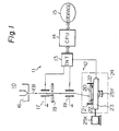
- Figure 1 illustrates an overall schematic view of a conventional electron beam exposure system 10.
- the electron beam exposure system 10 usually comprises two major parts, i.e., a processor 11 and an exposure assembly 12.
- the processor 11 is comprised of an interface equipment 13, a central processing unit 14, and a storage unit 15.
- the basic assembly of the exposure assembly 12 is a follows.
- An electron beam source 16 which radiates an electron beam EB which is injected into a blanking unit 17 cooperating with a blanking plate 18 provided with an aperture therein.
- the function of the blanking unit 17 is to permit or not to permit the EB to travel downward.
- the EB passing through the unit 17 is controlled by a deflection unit 19 to travel along a specified flying path, in accordance with a pattern data stored in the storage unit 15.
- the incident EB is applied to the surface of a workpiece 20.
- the workpiece 20 is held by a piece holder 21 at three or more, usually four, supporting points 22.
- the workpiece 20, together with the piece holder 21, is mounted on a stage 23.
- the members 20 through 23 are located inside a work chamber 24.
- the workpiece 20 is moved stepwise in an X axis direction and/or Y axis direction by an X axis drive motor 25X and a Y axis drive motor 25Y, to form the desired patterns on the entire surface of the workpiece 20 by the previously-mentioned step and repeat method.
- the workpiece 20 may be, as previously mentioned, a reticle, a master mask, or a wafer.
- a reticle a reticle
- a master mask a wafer.
- the present invention is described with reference to a master mask as a preferred example.
- the master mask is made from a blanked mask.
- the blanked mask is made of glass plate 1.5 mm or 2.3 mm in thickness (or synthetic quartz) having a low coefficient of expansion.
- the glass plate is larger in length, at each side, than the semiconductor wafer, which has a diameter of about 100 mm.
- a metal chromium (Cr) layer is formed on the entire surface of the glass plate by a sputtering method. An electron-resist-coated material is then covered over the surface of the Cr layer.
- the thus formed blanked mask is placed in the work chamber 24 so that the desired patterns can be drawn with the EB, by concurrently using the step and repeat method, to obtain the master mask.
- This method is carried out with the aid of the X and Y axis drive motors 24X and 24Y, constructed as pulse motors, and the like.
- the motors are driven with a very high positioning accuracy of less than about 0.1 um, by utilizing a suitable interferometer using, for example, an He-Ne laser.
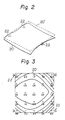
- Figure 2 is a perspective view of a blanked mask to be patterned, when supported at three points.
- the blanked mask 20, indicated by broken lines, represents a mask wherein no elastic deformation is exhibited. Note, the unevenness of the illustrated mask 20, caused by the elastic deformation, induces the previously-mentioned pitch error.
- Figure 3 is a plan view of the blanked mask to be patterned when supported at four points.
- the four supporting points 22 are illustrated as outside the mask, to clarify the locations of these points, but are actually located beneath the mask.
- a plurality of contour lines are illustrated on the mask 20, to depict the elastically deformed surface. Twenty-five points (marked +), for example, are plotted on the surface, with individual relative levels in height given in pm. These were measured from a centre level of 0.0 pm, where each side of the square surface is about 130 mm in length. Thus, each two adjacent contour lines exhibit a different level, by about 1 pm.
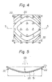
- Figure 4 is a plan view of the blanked mask to be patterned when supported at four points, showing contour lines and levels obtained by a technique different from that used in obtaining the data in Fig. 3. That is, the contour lines and levels shown in Fig. 4 are obtained in reference to an ideal plane which intersects the centre of the mask surface at least.
- the ideal plane can be defined by utilizing a well known least squares approximation method.
- the pitch error can be corrected with a high accuracy; as any deviation in the level of the surface of the mask itself can be measured.
- the pitch error correction according to the present invention is preferably achieved in reference to this ideal plane.
- the maximum deviation in level reaches about 5 pm, when the mask is 130 mm square.
- Figure 5 is a cross-section view of the mask taken along the line 5-5 shown in Fig. 4.
- the members 20 and 22 are identical to those shown in the previous figures.
- Reference numeral 51 denotes a neutral axis of the elastically deformed mask 20.
- Figure 5 clearly shows one basic mode of the elastic deformation which apparently produces the deflection by compression on the surface to be patterned by the EB. In this case, it should be noted that, on the surface of the mask, not only the deflection by compression, as illustrated in Fig. 5, but also the deflection by tension may be produced, as illustrated in Figs. 2 and 6. In the basic mode of elastic deformation shown in Fig. 5, the following equation (1) stands approximately.
- ⁇ L denotes the compression amount produced on the surface of the mask (AL also denotes the tension amount produced thereon where deflection by tension exists thereon), L denotes a span of one arc due to the deformation (in Fig. 5, L denotes a span between two supporting points 22), t denotes a thickness of the mask 20, and b denotes a bending amount.
- the equation (1) is taught by, for example, the disclosure on pages 86 and 87 of a "Proceeding of Interface '74, Kodak Microelectronics Seminar, H. R.
- a compression amount AL of about 0.38 pm is obtained when the parameter L is about 120 mm, b about 5 pm, and t about 2.3 mm.
- This compression amount (or tension amount) AL will induce patch errors in the pattern to be produced, if the mask 20 is placed on and is in contact with, via its resist coated surface, a wafer, because, at this time, elastic deformation is not created in the mask 20.
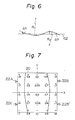
- Figure 6 depicts an arbitrary profile of the mask.
- the chain dotted line 61 indicates the profile of the mask, and the straight line 62 represents the least square approximated plane defined as the aforesaid ideal plane.
- the arc R 1 is similar to the arc shown in Fig. 5. This arc is produced by the deformation due to compression. Conversely, the arc R 2 is produced by the deformation due to tension.
- a radius R which is a representative of R 1 and R 2 , is an approximation radius of the bending curvature (refer to Fig.5), corresponding to said arc, of the mask surface.
- the radius R can be derived from the equation (1).
- the correction data for compensating the pitch error can be obtained in the manner mentioned hereinafter.
- the elastic deformation of the mask is first forcibly concentrated in either one of the X and Y directions. That is, the supporting points 22 are arranged in such a manner as to exhibit the deformation along one direction only.
- Figure 7 shows a preferred arrangement of the supporting points, according to the present invention.
- the processing for effecting the correction of the pitch error can be limited to one direction only of the two perpendicular directions.
- the supporting points 22A, 22A', 22B, and 22B' are arranged in such a manner as to suppress the deviation in level, along the Y direction, within about 0.5 ⁇ m. This may also be clarified with reference to the contour lines which extend nearly in parallel with the Y direction. For example, assuming that the mask 20 is 130 mm square and about 2.3 mm in thickness, the supporting points 22A, 22A' are located with a pitch of about 80 mm, and the supporting points 22B, 22B' are also located with the same pitch.
- the resultant pattern accuracy will be deteriorated by a pitch error of about 0.15 ⁇ m, when the mask 20 is laid flat on the wafer surface.
- the value of 0.15 um can also be estimated by using the previously recited equation (1). This poor accuracy can be improved by the present invention.
- the present invention is preferably put into practice as described below.
- the concerned pitch error correction can be effected by assuming that the pitch error, i.e., the compression amounts defined by the equation (1), are distributed with individual amounts which are proportional to the respective distances from the centre (refer to 0.0 in Fig 7) of the mask surface.
- the pitch error i.e., the compression amounts defined by the equation (1)
- the desired pattern can be reproduced correctly on the wafer surface as intended, even though the patterned mask is flattened thereon.
- the relationship between x and x' can be approximately expressed by the following equation (2).
- the second term exists as a correction value derived from the equation (1).
- this correction value is applied, as a correction data, to a predetermined pattern data to exposure an intended pattern on the surface of the workpiece.
- the pitch error correction can also be applied to a workpiece, for example, the mask 20 elastically deformed with the ball-like shape shown in Fig. 4, without adjusting the locations of the supporting points 20, as done in Fig. 7. That is, the present invention can be generally practiced as follows.
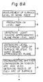
- Figures 8A and 8B are flow charts of successive processing steps for achieving the pitch error correction according to a first embodiment of the present invention.
- the surface level of the workpiece for example, the mask 20, is measured by a known measurement technique using a laser, an electrostatic microgauge, an air microgauge, or by inter- ferencefringes.
- step b the surface level data is measured at a plurality of specified portions along both X and Y axes (refer to each symbol + in Fig. 4) and then a level map is produced based on the thus measured surface level data.
- step c the least square approximated plane is defined with respect to the level map obtained in step b.
- step d the level difference data Ah (refer to Fig. 6) of the surface level relative to the least square approximated plane is obtained at each of the specified portions.
- step e the thus obtained level difference data is used to discriminate whether each specified portion exhibits a compression arc or a tension arc corresponding to the arc defined by the radius R 1 or R 2 in Fig. 6, respectively. Also, the radius of each arc is obtained.
- the radius can be estimated by assuming that the arc is a part of an actual circle. The actual circle can be determined from the level difference data.
- step f the correction data is obtained based on the data regarding the radii and the level differences.
- step g the correcion data is stored at the corresponding addresses in the memory areas of the storage unit.
- the addresses may be allotted to individual portions arranged with a pitch of, for example, 5 mm, on the surface of the workpiece, in conformity to the level map.
- step h each inherent pattern data is corrected by applying thereto the corresponding correction data read from the storage unit every time the related portion on the workpiece is exposed by the EB.
- step i the pattern is reproduced on the flat surface of the workpiece correctly and as intended, even though the mask 20 suffered from deleterious elastic deformation.
- the workpiece can be another material, such as a wafer.
- the greater the thickness of the workpiece the larger the amount of compression and tension. Therefore, the greater the thickness, the more remarkable are the advantages of the present invention.
- the thickness of the wafer is about 0.5 mm, while the thickness of the mask is about 2.3 mm.
- the pitch error correction by the present invention is useful to a great extent for a thick workpiece, such as a mask.
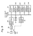
- Figure 9 is a block diagram exemplifying an electron beam exposure apparatus to be operated under the exposure method.
- the CPU 14, the storage unit 15, and the deflection unit 19 are functionally the same as those elements shown in Fig. 1.
- members 90 through 97 members 90 through 94 are particularly relevant to the present invention.
- the remaining members i.e., a high speed data processing unit 95, a digital/analog converter (DAC) 96, a read only memory (ROM) 97, and a data bus 98, are as used in a conventional automated exposure apparatus as illustrated in, for example, U.S. Patent No. 4,147,937, Fred K. Buelow et al, assigned to Fujitsu Limited.
- the pattern data desired is transferred to a data memory unit 90.
- This unit 90 momentarily stores the aforesaid inherent pattern data.
- the pattern data in the unit 15 is directly transferred to the data processing unit 95.
- the thus stored pattern data in the unit 90 is first modified by first through fourth memory units 91 through 94, and this thus modified pattern data is then supplied, instead of the conventional unmodified pattern data, to the unit 95.
- a measuring device 99 which measures the surface level of the workpiece 20 as previously mentioned, supplies the level data to the first memory unit 91, where the data is stored.
- the level data is processed by the CPU 14 in accordance with a newly employed program stored in the ROM 97 (refer to steps a and b).
- the CPU 14 reads the data in the first memory unit 91 and produces the least square approximated plane data in accordance with a corresponding program in the ROM 97.
- the plane data i.e., the ideal plane data, is stored in the second memory unit 92 (refer to step c).
- the CPU 14 reads the data in the first and second memory units 91 and 92 and produces the level differences in accordance with a corresponding program in the ROM 97.
- the thus produced level difference data is stored in the third memory unit 93 (refer to step d).
- the CPU 14 then processes the data in the memory units 92 and 93 to obtain the correction data, through steps e and f, in accordance with a corresponding program in the ROM 97.
- the thus produced correction data is stored in the fourth memory unit 94 (refer to step g).
- the CPU 14 synthesizes the inherent data from the unit 90 with the corresponding correction data from the unit 94, and produces the resultant corrected pattern data to be applied to the data processing unit 95.
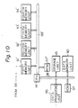
- Figure 10 illustrates a part of a modification of the apparatus shown in Fig. 9.
- the data memory unit 90 does not store the original pattern data from the storage unit 15, as in the apparatus shown in Fig. 9, but stores the corrected pattern data.
- the CPU 14 first operates to produce the corrected pattern in another field including members 91' through 94', 97', and 98' functionally identical to the members 91 through 94,97 and 98 shown in Fig. 9, respectively.
- the present invention is not limited to the result of equation (2) based on equation (1), which is derived from an analysis of a "bridge"-like lever, as shown in Fig. 5, and it is possible to use a modification of equation (2) based on a similar equation (1) derived from an analysis of a cantilever. Further, if a chip size in the wafer is less than 10 mm, it may not be necessary to apply the aforesaid pattern data correction to individual chips, but may be sufficient to apply the same data to the pitch size between each two adjacent chips.
- the pattern data correction of the present invention can be utilized in another field, such as a photo beam exposure system.
- it can be utilized in forecasting the actual pattern of a certain object, merely measuring the surface level of that object.
- the present invention can suppress to a great extent, the pitch error, due to the elastic deformation, produced in a pattern to be exposed. Therefore, the present invention is suitable for reproducing extremely precise and high density patterns, such as for VLSI's.
Description
- The present invention relates to the fabrication of semiconductor devices, especially very large scale integration (VSLI) devices, more particularly, it relates to a method and apparatus for patterning workpieces for producing such devices with a high accuracy.
- Recent research and development in semiconductor devices has concentrated on a higher degree of miniaturization and higher packaging densities. Such miniaturization and high density packaging of patterns can be realized by compound techniques such as patterning resists and etching the surfaces of the semiconductor substrates, using the thus patterned resists as masks.
- Among these techniques, patterning can be achieved very precisely i.e., to a limit smaller than a wavelength (0.5 um) of light, by employing an electron beam exposure system now in practical use. This electron beam exposure system has the following advantages. First, very precise patterning can be obtained with a minimum line width of about 0.1 pm, giving a higher resolution than that of light. Second, since it is possible to establish a very high positioning accuracy when a step and repeat method is used, each adjacent two sub- patterns and each adjacent two stripes can be finely aligned with each other. Third, because of the above second advantage, a plurality of sub- patterns can be accurately set up to obtain a considerably large size pattern. Fourth, the input data for defining each pattern can be easily adapted to computer processing. Fifth, the number of steps can be reduced below those needed in a light exposure system, thus minimizing the time required for making each device. Further, the electron beam exposure system itself can also work as a pattern generating system.
- Note, in view of the above advantages, the electron beam exposure system is used during the manufacture of the devices for dealing with a variety of workpieces, such as a reticle, a master mask, a wafer, and the like. The workpiece is usually supported at three or more points on the bottom thereof, to maintain the horizontality of the workpiece relative to the incident electron beam. However, in practice, this horizontality cannot be strictly maintained. This is because the surface of the workpiece is slightly deformed i.e., is not truly flat, due to its own weight, wherein the areas of the surface just above the supporting points can maintain the desired height, but areas apart from the supporting points necessarily drop to a level lower than that desired. Thus, elastic deformation by compression and/or elastic deformation by tension are created on the surface of the workpiece to be patterned by the electron beam. Such elastic deformations result in pattern pitch errors, and thereby, produce undesirable pattern distortion.
- The pitch errors may be caused by elastic deformation of the workpiece, nontrue flatness of the surface on which the workpiece is supported at the points, and nonuniformity of the thickness of the workpiece. Conventionally, small pitch errors, i.e., smaller than about 0.5 pm, are usually little or no problem, and therefore, such small pitch errors are disregarded. However, in VSLI devices, even pitch errors of about 0.5 µm cannot be permitted, and a higher positioning accuracy is demanded in order to attain a further miniaturization and a denser packaging of the integrated circuit (IC) patterns. Accordingly, the permissible error for positioning accuracy now becomes very limited and, for example, a pitch error of about 0.1 pm, at least, must be satisfied.
- Among the above-mentioned causes of pitch errors, the elastic deformation of the workpiece is the most difficult to correct. The remaining factors, i.e., the flatness and uniformity of thickness of the workpiece, may be easily improved by known techniques.
- An example of a known electron beam exposure apparatus is described in Proceedings of the IEEE
Vol 62, No. 10 October 1974, pages 1361-1383. - In accordance with one aspect of the present invention, a method for forming a pattern defined by predetermined pattern data on a workpiece mounted on supports is characterised by the steps of
- (1) obtaining level data for a surface of the workpiece;
- (2) determining from the level data correction data for application to the predetermined pattern data; and,
- (3) exposing the surface of the workpiece to an electron beam under control of the correction data and predetermined pattern data, whereby any elastic deformation of the workpiece is compensated for.
- In accordance with a second aspect of the present invention, electron beam exposure apparatus for forming a pattern on a workpiece mounted on supports comprises. a processor and an exposure assembly, the exposure assembly including at least a deflection unit, and the processor including at least a central processing unit, an interface equipment, a storage unit, and data buses interconnected therebetween, wherein the output from the processor controls the direction of an electron beam by way of the deflection unit characterised in that the storage unit comprises at least a first memory unit for storing first data representing level data of a surface of the workpiece, a second memory unit for storing second data generated by the central processing unit and indicating an ideal plane intersecting at least the centre of the surface to be patterned, a third memory unit for storing third data generated by the central processing unit and indicating level differences between the actual level of the surface at different positions and the level of the ideal plane, and a fourth memory unit for storing fourth data generated by the central processing unit and indicating correction data to be applied to a predetermined pattern data for forming the pattern on the workpiece.
- The present invention provides an electron beam exposure method and apparatus for compensating for pitch errors caused by the elastic deformation of the workpiece.
- The correction data may be applied to the predetermined pattern data prior to controlling the electron beam or the beam may be controlled separably by the correction data and the predetermined pattern data.
- The invention enables a desired pattern to be formed on the surface of the workpiece when the workpiece is subsequently flattened.
- Methods and apparatus in accordance with the present invention will now be described and contrasted with prior methods and apparatus with reference to the accompanying drawings, wherein:-
- Figure 1 illustrates an overall schematic view of a conventional electron beam exposure system;
- Figure 2 is a perspective view of a blanked mask to be patterned when supported at three points;
- Figure 3 is a plan view of a blanked mask to be patterned when supported at four points;
- Figure 4 is a plan view of a blanked mask to be patterned when supported at four points, showing contour lines and levels obtained by a technique different from that used in obtaining the data in Figure 3;
- "Figure 5 is a cross-section of the mask taken on the line 5-5 in Figure 4;
- Figure 6 depicts an arbitrary profile of the mask;
- Figure 7 shows an arrangement of the supporting points according to one example of the present invention;
- Figures. 8A and 8B are flow charts of successive processing steps for achieving the pitch error correction according to an embodiment of the present invention;
- Figure 9 is a block diagram exemplifying an electron beam exposure apparatus to be operated under the exposure method according to an example of the present invention; and,
- Figure 10 illustrates part of a modification of the apparatus shown in Figure 9.
- Figure 1 illustrates an overall schematic view of a conventional electron
beam exposure system 10. - The electron
beam exposure system 10 usually comprises two major parts, i.e., a processor 11 and anexposure assembly 12. The processor 11 is comprised of aninterface equipment 13, acentral processing unit 14, and astorage unit 15. The basic assembly of theexposure assembly 12 is a follows. - An
electron beam source 16, which radiates an electron beam EB which is injected into ablanking unit 17 cooperating with ablanking plate 18 provided with an aperture therein. The function of theblanking unit 17 is to permit or not to permit the EB to travel downward. The EB passing through theunit 17 is controlled by adeflection unit 19 to travel along a specified flying path, in accordance with a pattern data stored in thestorage unit 15. The incident EB is applied to the surface of aworkpiece 20. Theworkpiece 20 is held by a piece holder 21 at three or more, usually four, supportingpoints 22. Theworkpiece 20, together with the piece holder 21, is mounted on astage 23. Themembers 20 through 23 are located inside awork chamber 24. Since the incident angle of the EB is very small, e.g., several millira- dians, theworkpiece 20 is moved stepwise in an X axis direction and/or Y axis direction by an X axis drive motor 25X and a Yaxis drive motor 25Y, to form the desired patterns on the entire surface of theworkpiece 20 by the previously-mentioned step and repeat method. - The
workpiece 20 may be, as previously mentioned, a reticle, a master mask, or a wafer. The present invention is described with reference to a master mask as a preferred example. - The master mask is made from a blanked mask. The blanked mask is made of glass plate 1.5 mm or 2.3 mm in thickness (or synthetic quartz) having a low coefficient of expansion. The glass plate is larger in length, at each side, than the semiconductor wafer, which has a diameter of about 100 mm. A metal chromium (Cr) layer, about 60 nm to 90 nm in thickness, is formed on the entire surface of the glass plate by a sputtering method. An electron-resist-coated material is then covered over the surface of the Cr layer. The thus formed blanked mask is placed in the
work chamber 24 so that the desired patterns can be drawn with the EB, by concurrently using the step and repeat method, to obtain the master mask. This method is carried out with the aid of the X and Y axis drive motors 24X and 24Y, constructed as pulse motors, and the like. The motors are driven with a very high positioning accuracy of less than about 0.1 um, by utilizing a suitable interferometer using, for example, an He-Ne laser. - Figure 2 is a perspective view of a blanked mask to be patterned, when supported at three points. The
workpiece 20, i.e., the blanked mask indicated by solid-lines, represents an elastically deformed mask when located on the three supportingpoints 22. The blankedmask 20, indicated by broken lines, represents a mask wherein no elastic deformation is exhibited. Note, the unevenness of the illustratedmask 20, caused by the elastic deformation, induces the previously-mentioned pitch error. - Figure 3 is a plan view of the blanked mask to be patterned when supported at four points. The four
supporting points 22 are illustrated as outside the mask, to clarify the locations of these points, but are actually located beneath the mask. A plurality of contour lines are illustrated on themask 20, to depict the elastically deformed surface. Twenty-five points (marked +), for example, are plotted on the surface, with individual relative levels in height given in pm. These were measured from a centre level of 0.0 pm, where each side of the square surface is about 130 mm in length. Thus, each two adjacent contour lines exhibit a different level, by about 1 pm. - Figure 4 is a plan view of the blanked mask to be patterned when supported at four points, showing contour lines and levels obtained by a technique different from that used in obtaining the data in Fig. 3. That is, the contour lines and levels shown in Fig. 4 are obtained in reference to an ideal plane which intersects the centre of the mask surface at least. The ideal plane can be defined by utilizing a well known least squares approximation method. By using such an ideal plane, the pitch error can be corrected with a high accuracy; as any deviation in the level of the surface of the mask itself can be measured. Thus, the pitch error correction according to the present invention is preferably achieved in reference to this ideal plane.
- According to the example shown in Fig. 4, the maximum deviation in level reaches about 5 pm, when the mask is 130 mm square.
- Figure 5 is a cross-section view of the mask taken along the line 5-5 shown in Fig. 4. The
members Reference numeral 51 denotes a neutral axis of the elasticallydeformed mask 20. Figure 5 clearly shows one basic mode of the elastic deformation which apparently produces the deflection by compression on the surface to be patterned by the EB. In this case, it should be noted that, on the surface of the mask, not only the deflection by compression, as illustrated in Fig. 5, but also the deflection by tension may be produced, as illustrated in Figs. 2 and 6. In the basic mode of elastic deformation shown in Fig. 5, the following equation (1) stands approximately.
- Where, ΔL denotes the compression amount produced on the surface of the mask (AL also denotes the tension amount produced thereon where deflection by tension exists thereon), L denotes a span of one arc due to the deformation (in Fig. 5, L denotes a span between two supporting points 22), t denotes a thickness of the
mask 20, and b denotes a bending amount. The equation (1) is taught by, for example, the disclosure on pages 86 and 87 of a "Proceeding of Interface '74, Kodak Microelectronics Seminar, H. R. Rott- mann, entitled Advances in Contact and Proximity Printing." According to equation (1), a compression amount AL of about 0.38 pm is obtained when the parameter L is about 120 mm, b about 5 pm, and t about 2.3 mm. This compression amount (or tension amount) AL will induce patch errors in the pattern to be produced, if themask 20 is placed on and is in contact with, via its resist coated surface, a wafer, because, at this time, elastic deformation is not created in themask 20. - Figure 6 depicts an arbitrary profile of the mask. The chain dotted line 61 indicates the profile of the mask, and the
straight line 62 represents the least square approximated plane defined as the aforesaid ideal plane. In Fig. 6, the arc R1 is similar to the arc shown in Fig. 5. This arc is produced by the deformation due to compression. Conversely, the arc R2 is produced by the deformation due to tension. - A radius R, which is a representative of R1 and R2, is an approximation radius of the bending curvature (refer to Fig.5), corresponding to said arc, of the mask surface. The radius R can be derived from the equation (1). The correction data for compensating the pitch error can be obtained in the manner mentioned hereinafter.
- According to a preferred embodiment of the present invention, the elastic deformation of the mask is first forcibly concentrated in either one of the X and Y directions. That is, the supporting
points 22 are arranged in such a manner as to exhibit the deformation along one direction only. - Figure 7 shows a preferred arrangement of the supporting points, according to the present invention. In the preferred embodiment, the processing for effecting the correction of the pitch error can be limited to one direction only of the two perpendicular directions. In the embodiment shown in Fig. 7, the supporting
points mask 20 is 130 mm square and about 2.3 mm in thickness, the supportingpoints - Conversely, in the elastic deformation in the other direction X, shown in Fig. 7, a deformation by compression is exhibited to provide a level difference of about 2 um. In these circumstances, it may be thought possible to adjust each location of the supporting point pairs 22A, 22B and 22A' ,22B' in not only the Y direction (as men tioned above) but in also the X direction, to suppress the deviation in level in both the X and Y directions, and thereby minimizing the elastic deformation over the entire surface of the
mask 20. However, in practice, it is impossible to make the entire surface flat, but only results in giving a ball-like shape to the whole; as proved by experiment. - If the
mask 20 is set with the physical conditions shown in Fig. 7 and then rendered, as it is, to the EB exposure process, the resultant pattern accuracy will be deteriorated by a pitch error of about 0.15 µm, when themask 20 is laid flat on the wafer surface. The value of 0.15 um can also be estimated by using the previously recited equation (1). This poor accuracy can be improved by the present invention. - Taking the
mask 20 shown in Fig. 7 as an example, the present invention is preferably put into practice as described below. As shown in Fig. 7, deviation in the level of the mask surface varies smoothly and monotonously in one direction, i.e., the X direction. Therefore, the concerned pitch error correction can be effected by assuming that the pitch error, i.e., the compression amounts defined by the equation (1), are distributed with individual amounts which are proportional to the respective distances from the centre (refer to 0.0 in Fig 7) of the mask surface. Specifically, if a specified intended location x is modified by a corrected location x', the desired pattern can be reproduced correctly on the wafer surface as intended, even though the patterned mask is flattened thereon. The relationship between x and x' can be approximately expressed by the following equation (2).
- In the equation (2), the second term

- The pitch error correction can also be applied to a workpiece, for example, the
mask 20 elastically deformed with the ball-like shape shown in Fig. 4, without adjusting the locations of the supportingpoints 20, as done in Fig. 7. That is, the present invention can be generally practiced as follows. - Figures 8A and 8B are flow charts of successive processing steps for achieving the pitch error correction according to a first embodiment of the present invention.
- In step a, the surface level of the workpiece, for example, the
mask 20, is measured by a known measurement technique using a laser, an electrostatic microgauge, an air microgauge, or by inter- ferencefringes. - In step b, the surface level data is measured at a plurality of specified portions along both X and Y axes (refer to each symbol + in Fig. 4) and then a level map is produced based on the thus measured surface level data.
- In step c, the least square approximated plane is defined with respect to the level map obtained in step b.
- In step d, the level difference data Ah (refer to Fig. 6) of the surface level relative to the least square approximated plane is obtained at each of the specified portions.
- In step e, the thus obtained level difference data is used to discriminate whether each specified portion exhibits a compression arc or a tension arc corresponding to the arc defined by the radius R1 or R2 in Fig. 6, respectively. Also, the radius of each arc is obtained. Here, the radius can be estimated by assuming that the arc is a part of an actual circle. The actual circle can be determined from the level difference data.
- In step f, the correction data is obtained based on the data regarding the radii and the level differences.
- In step g, the correcion data is stored at the corresponding addresses in the memory areas of the storage unit. In this case, the addresses may be allotted to individual portions arranged with a pitch of, for example, 5 mm, on the surface of the workpiece, in conformity to the level map.
- In step h, each inherent pattern data is corrected by applying thereto the corresponding correction data read from the storage unit every time the related portion on the workpiece is exposed by the EB.
- In step i, the pattern is reproduced on the flat surface of the workpiece correctly and as intended, even though the
mask 20 suffered from deleterious elastic deformation. - Note the above explanations refer to the mask as the workpiece, however, the workpiece can be another material, such as a wafer. In this case, as is known, the greater the thickness of the workpiece, the larger the amount of compression and tension. Therefore, the greater the thickness, the more remarkable are the advantages of the present invention. Usually, the thickness of the wafer is about 0.5 mm, while the thickness of the mask is about 2.3 mm. Thus, the pitch error correction by the present invention is useful to a great extent for a thick workpiece, such as a mask.
- Figure 9 is a block diagram exemplifying an electron beam exposure apparatus to be operated under the exposure method. In Figure 9, the
CPU 14, thestorage unit 15, and thedeflection unit 19 are functionally the same as those elements shown in Fig. 1. Formembers 90 through 97,members 90 through 94 are particularly relevant to the present invention. The remaining members, i.e., a high speeddata processing unit 95, a digital/analog converter (DAC) 96, a read only memory (ROM) 97, and adata bus 98, are as used in a conventional automated exposure apparatus as illustrated in, for example, U.S. Patent No. 4,147,937, Fred K. Buelow et al, assigned to Fujitsu Limited. Thestorage unit 15, e.g., a disc memory unit, contains a large variety of predetermined pattern data. The pattern data desired is transferred to adata memory unit 90. Thisunit 90 momentarily stores the aforesaid inherent pattern data. In the prior art, the pattern data in theunit 15 is directly transferred to thedata processing unit 95. In the present case, however, the thus stored pattern data in theunit 90 is first modified by first throughfourth memory units 91 through 94, and this thus modified pattern data is then supplied, instead of the conventional unmodified pattern data, to theunit 95. A measuringdevice 99, which measures the surface level of theworkpiece 20 as previously mentioned, supplies the level data to thefirst memory unit 91, where the data is stored. The level data is processed by theCPU 14 in accordance with a newly employed program stored in the ROM 97 (refer to steps a and b). TheCPU 14 reads the data in thefirst memory unit 91 and produces the least square approximated plane data in accordance with a corresponding program in theROM 97. The plane data, i.e., the ideal plane data, is stored in the second memory unit 92 (refer to step c). TheCPU 14 reads the data in the first andsecond memory units 91 and 92 and produces the level differences in accordance with a corresponding program in theROM 97. The thus produced level difference data is stored in the third memory unit 93 (refer to step d). TheCPU 14 then processes the data in thememory units 92 and 93 to obtain the correction data, through steps e and f, in accordance with a corresponding program in theROM 97. The thus produced correction data is stored in the fourth memory unit 94 (refer to step g). Thereafter, theCPU 14 synthesizes the inherent data from theunit 90 with the corresponding correction data from theunit 94, and produces the resultant corrected pattern data to be applied to thedata processing unit 95. - Figure 10 illustrates a part of a modification of the apparatus shown in Fig. 9. In the modified apparatus, the
data memory unit 90 does not store the original pattern data from thestorage unit 15, as in the apparatus shown in Fig. 9, but stores the corrected pattern data. To accomplish this, theCPU 14 first operates to produce the corrected pattern in another field including members 91' through 94', 97', and 98' functionally identical to themembers 91 through 94,97 and 98 shown in Fig. 9, respectively. - The present invention is not limited to the result of equation (2) based on equation (1), which is derived from an analysis of a "bridge"-like lever, as shown in Fig. 5, and it is possible to use a modification of equation (2) based on a similar equation (1) derived from an analysis of a cantilever. Further, if a chip size in the wafer is less than 10 mm, it may not be necessary to apply the aforesaid pattern data correction to individual chips, but may be sufficient to apply the same data to the pitch size between each two adjacent chips.
- Note, the pattern data correction of the present invention can be utilized in another field, such as a photo beam exposure system. In addition, it can be utilized in forecasting the actual pattern of a certain object, merely measuring the surface level of that object.
- As mentioned above in detail, the present invention can suppress to a great extent, the pitch error, due to the elastic deformation, produced in a pattern to be exposed. Therefore, the present invention is suitable for reproducing extremely precise and high density patterns, such as for VLSI's.
Claims (11)
Applications Claiming Priority (2)
| Application Number | Priority Date | Filing Date | Title |
|---|---|---|---|
| JP58014086A JPS59150422A (en) | 1983-01-31 | 1983-01-31 | Exposure process |
| JP14086/83 | 1983-01-31 |
Publications (2)
| Publication Number | Publication Date |
|---|---|
| EP0115952A1 EP0115952A1 (en) | 1984-08-15 |
| EP0115952B1 true EP0115952B1 (en) | 1987-04-01 |
Family
ID=11851290
Family Applications (1)
| Application Number | Title | Priority Date | Filing Date |
|---|---|---|---|
| EP84300569A Expired EP0115952B1 (en) | 1983-01-31 | 1984-01-30 | Electron beam exposure method and apparatus |
Country Status (4)
| Country | Link |
|---|---|
| US (1) | US4678919A (en) |
| EP (1) | EP0115952B1 (en) |
| JP (1) | JPS59150422A (en) |
| DE (1) | DE3462955D1 (en) |
Families Citing this family (13)
| Publication number | Priority date | Publication date | Assignee | Title |
|---|---|---|---|---|
| JPS61177718A (en) * | 1985-02-04 | 1986-08-09 | Hitachi Ltd | Electron beam lithography equipment |
| US4846552A (en) * | 1986-04-16 | 1989-07-11 | The United States Of America As Represented By The Secretary Of The Air Force | Method of fabricating high efficiency binary planar optical elements |
| JP2540168B2 (en) * | 1987-09-25 | 1996-10-02 | 三菱電機株式会社 | Beam deflection position correction device |
| JPH0779075B2 (en) * | 1990-02-21 | 1995-08-23 | 株式会社東芝 | Electron beam exposure system |
| US5329130A (en) * | 1991-08-06 | 1994-07-12 | Fujitsu Limited | Charged particle beam exposure method and apparatus |
| US5646403A (en) * | 1994-10-28 | 1997-07-08 | Nikon Corporation | Scanning electron microscope |
| US5773836A (en) * | 1996-10-28 | 1998-06-30 | International Business Machines Corporation | Method for correcting placement errors in a lithography system |
| GB2339960B (en) * | 1998-07-16 | 2001-01-17 | Advantest Corp | Charged particle beam exposure apparatus and exposure method capable of highly accurate exposure in the presence of partial surface unevenness of the specimen |
| JP2000091225A (en) | 1998-07-16 | 2000-03-31 | Advantest Corp | Device and method for charged particle beam exposure |
| AU3815200A (en) * | 1999-04-01 | 2000-10-23 | Sigma-C Gmbh | Method for correcting image faults |
| JP2004361507A (en) * | 2003-06-02 | 2004-12-24 | Renesas Technology Corp | Method for manufacturing photomask and photomask drawing system |
| JP5087258B2 (en) * | 2005-11-04 | 2012-12-05 | 株式会社ニューフレアテクノロジー | Charged particle beam drawing method, charged particle beam drawing apparatus, positional deviation amount measuring method, and position measuring apparatus |
| JP4891804B2 (en) * | 2007-02-21 | 2012-03-07 | 日本電子株式会社 | Pattern drawing method |
Family Cites Families (9)
| Publication number | Priority date | Publication date | Assignee | Title |
|---|---|---|---|---|
| JPS5398781A (en) * | 1976-11-25 | 1978-08-29 | Jeol Ltd | Electron ray exposure unit |
| US4137459A (en) * | 1978-02-13 | 1979-01-30 | International Business Machines Corporation | Method and apparatus for applying focus correction in E-beam system |
| JPS55102228A (en) * | 1979-01-29 | 1980-08-05 | Nippon Telegr & Teleph Corp <Ntt> | Electron beam exposure device |
| NL7904580A (en) * | 1979-06-12 | 1980-12-16 | Philips Nv | DEVICE FOR WRITING PATTERNS IN A LAYER ON A SUBSTRATE WITH AN ELECTRICALLY CHARGED PARTICLE BUNDLE. |
| JPS5536990A (en) * | 1979-07-16 | 1980-03-14 | Toshiba Corp | Apparatus for applying electron beam |
| JPS5621321A (en) * | 1979-07-27 | 1981-02-27 | Fujitsu Ltd | Automatically setting method of focus and exposure coefficient of electron beam exposure apparatus |
| JPS5693318A (en) * | 1979-12-10 | 1981-07-28 | Fujitsu Ltd | Electron beam exposure device |
| JPS56124234A (en) * | 1980-03-05 | 1981-09-29 | Hitachi Ltd | Correcting method for electron beam deflection |
| JPS5787131A (en) * | 1980-11-20 | 1982-05-31 | Jeol Ltd | Exposing method of electron beam |
-
1983
- 1983-01-31 JP JP58014086A patent/JPS59150422A/en active Granted
-
1984
- 1984-01-30 EP EP84300569A patent/EP0115952B1/en not_active Expired
- 1984-01-30 DE DE8484300569T patent/DE3462955D1/en not_active Expired
-
1986
- 1986-07-14 US US06/883,425 patent/US4678919A/en not_active Expired - Lifetime
Also Published As
| Publication number | Publication date |
|---|---|
| DE3462955D1 (en) | 1987-05-07 |
| US4678919A (en) | 1987-07-07 |
| EP0115952A1 (en) | 1984-08-15 |
| JPH0352210B2 (en) | 1991-08-09 |
| JPS59150422A (en) | 1984-08-28 |
Similar Documents
| Publication | Publication Date | Title |
|---|---|---|
| EP0115952B1 (en) | Electron beam exposure method and apparatus | |
| US6225011B1 (en) | Method for manufacturing semiconductor devices utilizing plurality of exposure systems | |
| US4780617A (en) | Method for successive alignment of chip patterns on a substrate | |
| US5805866A (en) | Alignment method | |
| US5585925A (en) | Alignment method | |
| US20020042664A1 (en) | Evaluation method, position detection method, exposure method and device manufacturing method, and exposure apparatus | |
| US20170075230A1 (en) | Method and Apparatus for Fabricating Wafer By Calculating Process Correction Parameters | |
| US6859260B2 (en) | Method and system for improving focus accuracy in a lithography system | |
| EP2620976B1 (en) | Overlay model for aligning and exposing semiconductor wafers | |
| JP3393947B2 (en) | Semiconductor circuit pattern evaluation method and evaluation system, writing method, and writing system | |
| EP0130819B1 (en) | A method of positioning a beam to a specific portion of a semiconductor wafer | |
| US6221539B1 (en) | Mask pattern correction method and a recording medium which records a mask pattern correction program | |
| US20040070771A1 (en) | Focus control system | |
| US20040119956A1 (en) | Distortion measurement method and exposure apparatus | |
| US7456031B2 (en) | Exposure device, exposure method, and semiconductor device manufacturing method | |
| EP0611996A2 (en) | Phase shift mask and its inspection method | |
| US20040227916A1 (en) | Displacement correction apparatus, exposure system, exposure method and a computer program product | |
| US6741732B2 (en) | Exposure method and device manufacturing method using this exposure method | |
| US7109500B2 (en) | Mask pattern correction method, semiconductor device manufacturing method, mask manufacturing method and mask | |
| EP1205807A1 (en) | Exposure apparatus and exposure method | |
| EP0148784B1 (en) | Calibration of electron beam apparatus | |
| US4644170A (en) | Method of electron beam exposure | |
| US6182369B1 (en) | Pattern forming apparatus | |
| JP3445102B2 (en) | Exposure apparatus and device manufacturing method | |
| JP3462989B2 (en) | Photomask and method of making the same |
Legal Events
| Date | Code | Title | Description |
|---|---|---|---|
| PUAI | Public reference made under article 153(3) epc to a published international application that has entered the european phase |
Free format text: ORIGINAL CODE: 0009012 |
|
| AK | Designated contracting states |
Designated state(s): DE FR GB |
|
| 17P | Request for examination filed |
Effective date: 19841205 |
|
| GRAA | (expected) grant |
Free format text: ORIGINAL CODE: 0009210 |
|
| AK | Designated contracting states |
Kind code of ref document: B1 Designated state(s): DE FR GB |
|
| REF | Corresponds to: |
Ref document number: 3462955 Country of ref document: DE Date of ref document: 19870507 |
|
| ET | Fr: translation filed | ||
| PLBE | No opposition filed within time limit |
Free format text: ORIGINAL CODE: 0009261 |
|
| STAA | Information on the status of an ep patent application or granted ep patent |
Free format text: STATUS: NO OPPOSITION FILED WITHIN TIME LIMIT |
|
| 26N | No opposition filed | ||
| PGFP | Annual fee paid to national office [announced via postgrant information from national office to epo] |
Ref country code: DE Payment date: 19991231 Year of fee payment: 17 |
|
| PGFP | Annual fee paid to national office [announced via postgrant information from national office to epo] |
Ref country code: FR Payment date: 20000112 Year of fee payment: 17 |
|
| PGFP | Annual fee paid to national office [announced via postgrant information from national office to epo] |
Ref country code: GB Payment date: 20000126 Year of fee payment: 17 |
|
| PG25 | Lapsed in a contracting state [announced via postgrant information from national office to epo] |
Ref country code: GB Free format text: LAPSE BECAUSE OF NON-PAYMENT OF DUE FEES Effective date: 20010130 |
|
| GBPC | Gb: european patent ceased through non-payment of renewal fee |
Effective date: 20010130 |
|
| PG25 | Lapsed in a contracting state [announced via postgrant information from national office to epo] |
Ref country code: FR Free format text: LAPSE BECAUSE OF NON-PAYMENT OF DUE FEES Effective date: 20010928 |
|
| PG25 | Lapsed in a contracting state [announced via postgrant information from national office to epo] |
Ref country code: DE Free format text: LAPSE BECAUSE OF NON-PAYMENT OF DUE FEES Effective date: 20011101 |
|
| REG | Reference to a national code |
Ref country code: FR Ref legal event code: ST |