EP0117111A2 - Semiconductor device assembly - Google Patents
Semiconductor device assembly Download PDFInfo
- Publication number
- EP0117111A2 EP0117111A2 EP84300895A EP84300895A EP0117111A2 EP 0117111 A2 EP0117111 A2 EP 0117111A2 EP 84300895 A EP84300895 A EP 84300895A EP 84300895 A EP84300895 A EP 84300895A EP 0117111 A2 EP0117111 A2 EP 0117111A2
- Authority
- EP
- European Patent Office
- Prior art keywords
- package
- conductor
- semiconductor device
- pads
- circuit board
- Prior art date
- Legal status (The legal status is an assumption and is not a legal conclusion. Google has not performed a legal analysis and makes no representation as to the accuracy of the status listed.)
- Granted
Links
Images

Classifications
-
- H—ELECTRICITY
- H01—ELECTRIC ELEMENTS
- H01L—SEMICONDUCTOR DEVICES NOT COVERED BY CLASS H10
- H01L24/00—Arrangements for connecting or disconnecting semiconductor or solid-state bodies; Methods or apparatus related thereto
- H01L24/01—Means for bonding being attached to, or being formed on, the surface to be connected, e.g. chip-to-package, die-attach, "first-level" interconnects; Manufacturing methods related thereto
- H01L24/26—Layer connectors, e.g. plate connectors, solder or adhesive layers; Manufacturing methods related thereto
- H01L24/31—Structure, shape, material or disposition of the layer connectors after the connecting process
- H01L24/32—Structure, shape, material or disposition of the layer connectors after the connecting process of an individual layer connector
-
- H—ELECTRICITY
- H01—ELECTRIC ELEMENTS
- H01L—SEMICONDUCTOR DEVICES NOT COVERED BY CLASS H10
- H01L23/00—Details of semiconductor or other solid state devices
- H01L23/02—Containers; Seals
- H01L23/04—Containers; Seals characterised by the shape of the container or parts, e.g. caps, walls
- H01L23/053—Containers; Seals characterised by the shape of the container or parts, e.g. caps, walls the container being a hollow construction and having an insulating or insulated base as a mounting for the semiconductor body
- H01L23/057—Containers; Seals characterised by the shape of the container or parts, e.g. caps, walls the container being a hollow construction and having an insulating or insulated base as a mounting for the semiconductor body the leads being parallel to the base
-
- H—ELECTRICITY
- H01—ELECTRIC ELEMENTS
- H01L—SEMICONDUCTOR DEVICES NOT COVERED BY CLASS H10
- H01L23/00—Details of semiconductor or other solid state devices
- H01L23/48—Arrangements for conducting electric current to or from the solid state body in operation, e.g. leads, terminal arrangements ; Selection of materials therefor
- H01L23/488—Arrangements for conducting electric current to or from the solid state body in operation, e.g. leads, terminal arrangements ; Selection of materials therefor consisting of soldered or bonded constructions
- H01L23/498—Leads, i.e. metallisations or lead-frames on insulating substrates, e.g. chip carriers
- H01L23/49811—Additional leads joined to the metallisation on the insulating substrate, e.g. pins, bumps, wires, flat leads
-
- H—ELECTRICITY
- H01—ELECTRIC ELEMENTS
- H01L—SEMICONDUCTOR DEVICES NOT COVERED BY CLASS H10
- H01L23/00—Details of semiconductor or other solid state devices
- H01L23/52—Arrangements for conducting electric current within the device in operation from one component to another, i.e. interconnections, e.g. wires, lead frames
- H01L23/538—Arrangements for conducting electric current within the device in operation from one component to another, i.e. interconnections, e.g. wires, lead frames the interconnection structure between a plurality of semiconductor chips being formed on, or in, insulating substrates
- H01L23/5385—Assembly of a plurality of insulating substrates
-
- H—ELECTRICITY
- H05—ELECTRIC TECHNIQUES NOT OTHERWISE PROVIDED FOR
- H05K—PRINTED CIRCUITS; CASINGS OR CONSTRUCTIONAL DETAILS OF ELECTRIC APPARATUS; MANUFACTURE OF ASSEMBLAGES OF ELECTRICAL COMPONENTS
- H05K3/00—Apparatus or processes for manufacturing printed circuits
- H05K3/30—Assembling printed circuits with electric components, e.g. with resistor
- H05K3/32—Assembling printed circuits with electric components, e.g. with resistor electrically connecting electric components or wires to printed circuits
- H05K3/34—Assembling printed circuits with electric components, e.g. with resistor electrically connecting electric components or wires to printed circuits by soldering
- H05K3/341—Surface mounted components
- H05K3/3421—Leaded components
- H05K3/3426—Leaded components characterised by the leads
-
- H—ELECTRICITY
- H01—ELECTRIC ELEMENTS
- H01L—SEMICONDUCTOR DEVICES NOT COVERED BY CLASS H10
- H01L2224/00—Indexing scheme for arrangements for connecting or disconnecting semiconductor or solid-state bodies and methods related thereto as covered by H01L24/00
- H01L2224/01—Means for bonding being attached to, or being formed on, the surface to be connected, e.g. chip-to-package, die-attach, "first-level" interconnects; Manufacturing methods related thereto
- H01L2224/26—Layer connectors, e.g. plate connectors, solder or adhesive layers; Manufacturing methods related thereto
- H01L2224/2612—Auxiliary members for layer connectors, e.g. spacers
-
- H—ELECTRICITY
- H01—ELECTRIC ELEMENTS
- H01L—SEMICONDUCTOR DEVICES NOT COVERED BY CLASS H10
- H01L2224/00—Indexing scheme for arrangements for connecting or disconnecting semiconductor or solid-state bodies and methods related thereto as covered by H01L24/00
- H01L2224/01—Means for bonding being attached to, or being formed on, the surface to be connected, e.g. chip-to-package, die-attach, "first-level" interconnects; Manufacturing methods related thereto
- H01L2224/42—Wire connectors; Manufacturing methods related thereto
- H01L2224/44—Structure, shape, material or disposition of the wire connectors prior to the connecting process
- H01L2224/45—Structure, shape, material or disposition of the wire connectors prior to the connecting process of an individual wire connector
- H01L2224/45001—Core members of the connector
- H01L2224/45099—Material
- H01L2224/451—Material with a principal constituent of the material being a metal or a metalloid, e.g. boron (B), silicon (Si), germanium (Ge), arsenic (As), antimony (Sb), tellurium (Te) and polonium (Po), and alloys thereof
- H01L2224/45138—Material with a principal constituent of the material being a metal or a metalloid, e.g. boron (B), silicon (Si), germanium (Ge), arsenic (As), antimony (Sb), tellurium (Te) and polonium (Po), and alloys thereof the principal constituent melting at a temperature of greater than or equal to 950°C and less than 1550°C
- H01L2224/45147—Copper (Cu) as principal constituent
-
- H—ELECTRICITY
- H01—ELECTRIC ELEMENTS
- H01L—SEMICONDUCTOR DEVICES NOT COVERED BY CLASS H10
- H01L2224/00—Indexing scheme for arrangements for connecting or disconnecting semiconductor or solid-state bodies and methods related thereto as covered by H01L24/00
- H01L2224/01—Means for bonding being attached to, or being formed on, the surface to be connected, e.g. chip-to-package, die-attach, "first-level" interconnects; Manufacturing methods related thereto
- H01L2224/42—Wire connectors; Manufacturing methods related thereto
- H01L2224/47—Structure, shape, material or disposition of the wire connectors after the connecting process
- H01L2224/48—Structure, shape, material or disposition of the wire connectors after the connecting process of an individual wire connector
- H01L2224/4805—Shape
- H01L2224/4809—Loop shape
- H01L2224/48091—Arched
-
- H—ELECTRICITY
- H01—ELECTRIC ELEMENTS
- H01L—SEMICONDUCTOR DEVICES NOT COVERED BY CLASS H10
- H01L2224/00—Indexing scheme for arrangements for connecting or disconnecting semiconductor or solid-state bodies and methods related thereto as covered by H01L24/00
- H01L2224/01—Means for bonding being attached to, or being formed on, the surface to be connected, e.g. chip-to-package, die-attach, "first-level" interconnects; Manufacturing methods related thereto
- H01L2224/42—Wire connectors; Manufacturing methods related thereto
- H01L2224/47—Structure, shape, material or disposition of the wire connectors after the connecting process
- H01L2224/48—Structure, shape, material or disposition of the wire connectors after the connecting process of an individual wire connector
- H01L2224/481—Disposition
- H01L2224/48151—Connecting between a semiconductor or solid-state body and an item not being a semiconductor or solid-state body, e.g. chip-to-substrate, chip-to-passive
- H01L2224/48221—Connecting between a semiconductor or solid-state body and an item not being a semiconductor or solid-state body, e.g. chip-to-substrate, chip-to-passive the body and the item being stacked
- H01L2224/48225—Connecting between a semiconductor or solid-state body and an item not being a semiconductor or solid-state body, e.g. chip-to-substrate, chip-to-passive the body and the item being stacked the item being non-metallic, e.g. insulating substrate with or without metallisation
- H01L2224/48227—Connecting between a semiconductor or solid-state body and an item not being a semiconductor or solid-state body, e.g. chip-to-substrate, chip-to-passive the body and the item being stacked the item being non-metallic, e.g. insulating substrate with or without metallisation connecting the wire to a bond pad of the item
-
- H—ELECTRICITY
- H01—ELECTRIC ELEMENTS
- H01L—SEMICONDUCTOR DEVICES NOT COVERED BY CLASS H10
- H01L24/00—Arrangements for connecting or disconnecting semiconductor or solid-state bodies; Methods or apparatus related thereto
- H01L24/01—Means for bonding being attached to, or being formed on, the surface to be connected, e.g. chip-to-package, die-attach, "first-level" interconnects; Manufacturing methods related thereto
- H01L24/42—Wire connectors; Manufacturing methods related thereto
- H01L24/44—Structure, shape, material or disposition of the wire connectors prior to the connecting process
- H01L24/45—Structure, shape, material or disposition of the wire connectors prior to the connecting process of an individual wire connector
-
- H—ELECTRICITY
- H01—ELECTRIC ELEMENTS
- H01L—SEMICONDUCTOR DEVICES NOT COVERED BY CLASS H10
- H01L24/00—Arrangements for connecting or disconnecting semiconductor or solid-state bodies; Methods or apparatus related thereto
- H01L24/01—Means for bonding being attached to, or being formed on, the surface to be connected, e.g. chip-to-package, die-attach, "first-level" interconnects; Manufacturing methods related thereto
- H01L24/42—Wire connectors; Manufacturing methods related thereto
- H01L24/47—Structure, shape, material or disposition of the wire connectors after the connecting process
- H01L24/48—Structure, shape, material or disposition of the wire connectors after the connecting process of an individual wire connector
-
- H—ELECTRICITY
- H01—ELECTRIC ELEMENTS
- H01L—SEMICONDUCTOR DEVICES NOT COVERED BY CLASS H10
- H01L2924/00—Indexing scheme for arrangements or methods for connecting or disconnecting semiconductor or solid-state bodies as covered by H01L24/00
- H01L2924/01—Chemical elements
- H01L2924/01006—Carbon [C]
-
- H—ELECTRICITY
- H01—ELECTRIC ELEMENTS
- H01L—SEMICONDUCTOR DEVICES NOT COVERED BY CLASS H10
- H01L2924/00—Indexing scheme for arrangements or methods for connecting or disconnecting semiconductor or solid-state bodies as covered by H01L24/00
- H01L2924/01—Chemical elements
- H01L2924/01029—Copper [Cu]
-
- H—ELECTRICITY
- H01—ELECTRIC ELEMENTS
- H01L—SEMICONDUCTOR DEVICES NOT COVERED BY CLASS H10
- H01L2924/00—Indexing scheme for arrangements or methods for connecting or disconnecting semiconductor or solid-state bodies as covered by H01L24/00
- H01L2924/01—Chemical elements
- H01L2924/01033—Arsenic [As]
-
- H—ELECTRICITY
- H01—ELECTRIC ELEMENTS
- H01L—SEMICONDUCTOR DEVICES NOT COVERED BY CLASS H10
- H01L2924/00—Indexing scheme for arrangements or methods for connecting or disconnecting semiconductor or solid-state bodies as covered by H01L24/00
- H01L2924/01—Chemical elements
- H01L2924/01042—Molybdenum [Mo]
-
- H—ELECTRICITY
- H01—ELECTRIC ELEMENTS
- H01L—SEMICONDUCTOR DEVICES NOT COVERED BY CLASS H10
- H01L2924/00—Indexing scheme for arrangements or methods for connecting or disconnecting semiconductor or solid-state bodies as covered by H01L24/00
- H01L2924/01—Chemical elements
- H01L2924/01047—Silver [Ag]
-
- H—ELECTRICITY
- H01—ELECTRIC ELEMENTS
- H01L—SEMICONDUCTOR DEVICES NOT COVERED BY CLASS H10
- H01L2924/00—Indexing scheme for arrangements or methods for connecting or disconnecting semiconductor or solid-state bodies as covered by H01L24/00
- H01L2924/01—Chemical elements
- H01L2924/0105—Tin [Sn]
-
- H—ELECTRICITY
- H01—ELECTRIC ELEMENTS
- H01L—SEMICONDUCTOR DEVICES NOT COVERED BY CLASS H10
- H01L2924/00—Indexing scheme for arrangements or methods for connecting or disconnecting semiconductor or solid-state bodies as covered by H01L24/00
- H01L2924/01—Chemical elements
- H01L2924/01057—Lanthanum [La]
-
- H—ELECTRICITY
- H01—ELECTRIC ELEMENTS
- H01L—SEMICONDUCTOR DEVICES NOT COVERED BY CLASS H10
- H01L2924/00—Indexing scheme for arrangements or methods for connecting or disconnecting semiconductor or solid-state bodies as covered by H01L24/00
- H01L2924/01—Chemical elements
- H01L2924/01074—Tungsten [W]
-
- H—ELECTRICITY
- H01—ELECTRIC ELEMENTS
- H01L—SEMICONDUCTOR DEVICES NOT COVERED BY CLASS H10
- H01L2924/00—Indexing scheme for arrangements or methods for connecting or disconnecting semiconductor or solid-state bodies as covered by H01L24/00
- H01L2924/01—Chemical elements
- H01L2924/01078—Platinum [Pt]
-
- H—ELECTRICITY
- H01—ELECTRIC ELEMENTS
- H01L—SEMICONDUCTOR DEVICES NOT COVERED BY CLASS H10
- H01L2924/00—Indexing scheme for arrangements or methods for connecting or disconnecting semiconductor or solid-state bodies as covered by H01L24/00
- H01L2924/01—Chemical elements
- H01L2924/01079—Gold [Au]
-
- H—ELECTRICITY
- H01—ELECTRIC ELEMENTS
- H01L—SEMICONDUCTOR DEVICES NOT COVERED BY CLASS H10
- H01L2924/00—Indexing scheme for arrangements or methods for connecting or disconnecting semiconductor or solid-state bodies as covered by H01L24/00
- H01L2924/01—Chemical elements
- H01L2924/01082—Lead [Pb]
-
- H—ELECTRICITY
- H01—ELECTRIC ELEMENTS
- H01L—SEMICONDUCTOR DEVICES NOT COVERED BY CLASS H10
- H01L2924/00—Indexing scheme for arrangements or methods for connecting or disconnecting semiconductor or solid-state bodies as covered by H01L24/00
- H01L2924/10—Details of semiconductor or other solid state devices to be connected
- H01L2924/11—Device type
- H01L2924/14—Integrated circuits
-
- H—ELECTRICITY
- H01—ELECTRIC ELEMENTS
- H01L—SEMICONDUCTOR DEVICES NOT COVERED BY CLASS H10
- H01L2924/00—Indexing scheme for arrangements or methods for connecting or disconnecting semiconductor or solid-state bodies as covered by H01L24/00
- H01L2924/15—Details of package parts other than the semiconductor or other solid state devices to be connected
- H01L2924/151—Die mounting substrate
- H01L2924/1515—Shape
- H01L2924/15153—Shape the die mounting substrate comprising a recess for hosting the device
-
- H—ELECTRICITY
- H01—ELECTRIC ELEMENTS
- H01L—SEMICONDUCTOR DEVICES NOT COVERED BY CLASS H10
- H01L2924/00—Indexing scheme for arrangements or methods for connecting or disconnecting semiconductor or solid-state bodies as covered by H01L24/00
- H01L2924/15—Details of package parts other than the semiconductor or other solid state devices to be connected
- H01L2924/151—Die mounting substrate
- H01L2924/1517—Multilayer substrate
-
- H—ELECTRICITY
- H01—ELECTRIC ELEMENTS
- H01L—SEMICONDUCTOR DEVICES NOT COVERED BY CLASS H10
- H01L2924/00—Indexing scheme for arrangements or methods for connecting or disconnecting semiconductor or solid-state bodies as covered by H01L24/00
- H01L2924/15—Details of package parts other than the semiconductor or other solid state devices to be connected
- H01L2924/151—Die mounting substrate
- H01L2924/153—Connection portion
- H01L2924/1531—Connection portion the connection portion being formed only on the surface of the substrate opposite to the die mounting surface
- H01L2924/15311—Connection portion the connection portion being formed only on the surface of the substrate opposite to the die mounting surface being a ball array, e.g. BGA
-
- H—ELECTRICITY
- H01—ELECTRIC ELEMENTS
- H01L—SEMICONDUCTOR DEVICES NOT COVERED BY CLASS H10
- H01L2924/00—Indexing scheme for arrangements or methods for connecting or disconnecting semiconductor or solid-state bodies as covered by H01L24/00
- H01L2924/15—Details of package parts other than the semiconductor or other solid state devices to be connected
- H01L2924/151—Die mounting substrate
- H01L2924/153—Connection portion
- H01L2924/1531—Connection portion the connection portion being formed only on the surface of the substrate opposite to the die mounting surface
- H01L2924/15312—Connection portion the connection portion being formed only on the surface of the substrate opposite to the die mounting surface being a pin array, e.g. PGA
-
- H—ELECTRICITY
- H01—ELECTRIC ELEMENTS
- H01L—SEMICONDUCTOR DEVICES NOT COVERED BY CLASS H10
- H01L2924/00—Indexing scheme for arrangements or methods for connecting or disconnecting semiconductor or solid-state bodies as covered by H01L24/00
- H01L2924/15—Details of package parts other than the semiconductor or other solid state devices to be connected
- H01L2924/151—Die mounting substrate
- H01L2924/153—Connection portion
- H01L2924/1532—Connection portion the connection portion being formed on the die mounting surface of the substrate
-
- H—ELECTRICITY
- H01—ELECTRIC ELEMENTS
- H01L—SEMICONDUCTOR DEVICES NOT COVERED BY CLASS H10
- H01L2924/00—Indexing scheme for arrangements or methods for connecting or disconnecting semiconductor or solid-state bodies as covered by H01L24/00
- H01L2924/15—Details of package parts other than the semiconductor or other solid state devices to be connected
- H01L2924/151—Die mounting substrate
- H01L2924/156—Material
- H01L2924/15786—Material with a principal constituent of the material being a non metallic, non metalloid inorganic material
- H01L2924/15787—Ceramics, e.g. crystalline carbides, nitrides or oxides
-
- H—ELECTRICITY
- H01—ELECTRIC ELEMENTS
- H01L—SEMICONDUCTOR DEVICES NOT COVERED BY CLASS H10
- H01L2924/00—Indexing scheme for arrangements or methods for connecting or disconnecting semiconductor or solid-state bodies as covered by H01L24/00
- H01L2924/15—Details of package parts other than the semiconductor or other solid state devices to be connected
- H01L2924/161—Cap
- H01L2924/1615—Shape
- H01L2924/16195—Flat cap [not enclosing an internal cavity]
-
- H—ELECTRICITY
- H01—ELECTRIC ELEMENTS
- H01L—SEMICONDUCTOR DEVICES NOT COVERED BY CLASS H10
- H01L2924/00—Indexing scheme for arrangements or methods for connecting or disconnecting semiconductor or solid-state bodies as covered by H01L24/00
- H01L2924/30—Technical effects
- H01L2924/35—Mechanical effects
- H01L2924/351—Thermal stress
-
- H—ELECTRICITY
- H05—ELECTRIC TECHNIQUES NOT OTHERWISE PROVIDED FOR
- H05K—PRINTED CIRCUITS; CASINGS OR CONSTRUCTIONAL DETAILS OF ELECTRIC APPARATUS; MANUFACTURE OF ASSEMBLAGES OF ELECTRICAL COMPONENTS
- H05K2201/00—Indexing scheme relating to printed circuits covered by H05K1/00
- H05K2201/10—Details of components or other objects attached to or integrated in a printed circuit board
- H05K2201/10613—Details of electrical connections of non-printed components, e.g. special leads
- H05K2201/10621—Components characterised by their electrical contacts
- H05K2201/10704—Pin grid array [PGA]
-
- H—ELECTRICITY
- H05—ELECTRIC TECHNIQUES NOT OTHERWISE PROVIDED FOR
- H05K—PRINTED CIRCUITS; CASINGS OR CONSTRUCTIONAL DETAILS OF ELECTRIC APPARATUS; MANUFACTURE OF ASSEMBLAGES OF ELECTRICAL COMPONENTS
- H05K2201/00—Indexing scheme relating to printed circuits covered by H05K1/00
- H05K2201/10—Details of components or other objects attached to or integrated in a printed circuit board
- H05K2201/10613—Details of electrical connections of non-printed components, e.g. special leads
- H05K2201/10742—Details of leads
- H05K2201/10886—Other details
- H05K2201/10909—Materials of terminal, e.g. of leads or electrodes of components
-
- H—ELECTRICITY
- H05—ELECTRIC TECHNIQUES NOT OTHERWISE PROVIDED FOR
- H05K—PRINTED CIRCUITS; CASINGS OR CONSTRUCTIONAL DETAILS OF ELECTRIC APPARATUS; MANUFACTURE OF ASSEMBLAGES OF ELECTRICAL COMPONENTS
- H05K2201/00—Indexing scheme relating to printed circuits covered by H05K1/00
- H05K2201/20—Details of printed circuits not provided for in H05K2201/01 - H05K2201/10
- H05K2201/2081—Compound repelling a metal, e.g. solder
-
- Y—GENERAL TAGGING OF NEW TECHNOLOGICAL DEVELOPMENTS; GENERAL TAGGING OF CROSS-SECTIONAL TECHNOLOGIES SPANNING OVER SEVERAL SECTIONS OF THE IPC; TECHNICAL SUBJECTS COVERED BY FORMER USPC CROSS-REFERENCE ART COLLECTIONS [XRACs] AND DIGESTS
- Y02—TECHNOLOGIES OR APPLICATIONS FOR MITIGATION OR ADAPTATION AGAINST CLIMATE CHANGE
- Y02P—CLIMATE CHANGE MITIGATION TECHNOLOGIES IN THE PRODUCTION OR PROCESSING OF GOODS
- Y02P70/00—Climate change mitigation technologies in the production process for final industrial or consumer products
- Y02P70/50—Manufacturing or production processes characterised by the final manufactured product
Definitions
- the present invention relates to packaging of a semiconductor device, and more particularly to an assembly of a package connected to a circuit board.
- leadless packages also known as chip carriers, have come into increasing use for accommodating integrated circuits (IC), large-scale integrated circuits (LSI ), and similar devices.
- IC integrated circuits
- LSI large-scale integrated circuits
- leadless packages accommodate an IC chip and outer contact pads of the leadless package are electrically connected to a circuit board by soldering. They therefore can be used in popular assembly processes.
- the provision of the contact pads as the conducting elements in place of outer leads enables a more compact structure. Therefore, such packages can be mounted at a higher density on a circuit board, compared with other packages. This highly prized feature has resulted in leadless packages being widely used in a broad range of fields.
- a semiconductor device assembly comprising:
- the present invention also embraces a semiconductor device package for use in such an assembly comprising a semiconductor chip
- Figure 1A is a partial cross-sectional view of a conventional semiconductor device assembly comprising a plurality of LSI's in packages and a circuit board.
- FIG. lA there is a package 1 electrically connected to a circuit board 2 through conductor pads 3 and solder 4.
- Reference numerals 5, 6, 7 and 8 denote an IC chip, wiring, a cap, and a heat sinking plate, respectively.
- Connecting electrodes 9 provided on the circuit board 2 are connected to the conductor pads 3 of the package 1 by the solder 4, which has a thickness of about 50 ⁇ m.
- the soldered connecting portion When thermal shock is generated during the operation of the circuit, the soldered connecting portion sometimes breaks, e.g., the solder cracks and falls off or the connecting electrode 9 are separated from the circuit board 2.
- the main reason for the heat-induced breakage is that the circuit board 2 is made of epoxy, polyimide, or other organic resins, which have a large thermal expansion coefficient, while the package 1 is made of ceramic, which has a small thermal expansion coefficient. Thus, the stress is given to the soldered connecting portion.
- the circuit board 2 can be made of ceramic too, which would eliminate the stress problem of thus breakage of the soldered connecting portions, however ceramic has high dielectric constant and would thus slow down the operation of the electronic circuits. Thus, ceramic is unsuitable for circuit boards except in special cases.
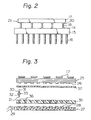
- FIG. 2 is a schematic view of a semiconductor device disclosed in IBM Technical Disclosure Bulletin vol. 18 No. 5 October 1975 PP 1379-1380.
- a semiconductor device 17 is mounted on and connected to a carrier 15 provided with pins 16 through a plurality of flexible strands 18.
- the bottom ends of the flexible strands 18 are aligned with solder mounds 19 on the top surface of the carrier 15.
- the top ends of the flexible strands 18 are connected to solder mounds 20 on the semiconductor device 17.
- the flexible strands form an electrical connection between the package and substrate. They are typically formed of thin copper wire.
- the strands are not, however, strong enough to be used advantageously as connecting portions between a package and circuit board. That is, since the strands are flexible, it becomes very complicated to assemble these flexible strands 18 to the semiconductor device 17 and the carrier 15.
- this publication discloses a complicated method where an special interposer 16 is used for assembling. And also, the flexible strands 18 have a demerit in which, the structure is weak about the kinetic intensity against the pressure 21 (horizontal direction).
- Figure 3 shows a disclosed conventional semiconductor device assembly disclosed in IBM Technical Disclosure Bullet vol. 19 No. 4 September 1976 PP 1207-1271.
- a multilayer ceramic substrate 25 with semiconductor devices 17 mounted on the top surface is provided with a plurality of pads 26 on the bottom surface.
- the multilayer ceramic substrate 25 is electrically connected to a multilayer laminated input/output distribution board 27 provided with pads 28 and wiring 29 through a spring-biased pin contact element 30 which includes a pair of slidably mounted pins 31 biased by a suitable spring 32 including a flange 33.
- the spring-biased pin contact element 30 is mounted in a socket board 35 provided with a suitable aperture 36.
- a socket retainer board 37 is disposed over the element 30 retaining it in position.
- Such a structure is not suitable for high density integration. The reason for that is that the socket board 35 must include the apertures 36 to accommodate the flanges 33. Making apertures for connecting pins and flanges means a reduction of pin density and an increase of the package size of the semiconductor device.
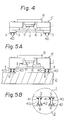
- Figure 4 is a cross-sectional view of an embodiment of a package according to the present invention.
- a package 1 is provided with conductor pins 40 through conductor pads 3.
- the conductor pins 40 are brazed to the conductor pads 3.
- Elements the same as in Fig. lA are denoted by the same reference numerals.
- the package of Fig. 4 is soldered through the conductor pins 40 to pads 9 provided on the top surface of the circuit board 2, as shown in Fig. 5A.
- Figure 5B is an enlarged cross-sectional view of the connecting portions shown in Fig. 5A.
- the package 1 and the circuit board 2 have conductor pads 3 and 9 on the respective surface thereof.
- the conductor pads 3 of the package 1 are formed as a metallized layer during sintering of the ceramic substrate and are plated with nickel.
- the conductor pins 40 are brazed to the metallized conductor pads 3 with silver alloy 41, such as of silver and copper, at a brazing temperature of 800°C to.850°C, the conductor pins 40 are fixed to the surface of the conductor pins 3 under the substantially vertical contact condition conductor pads 3. Then, the surface of the conductor pads 3, conductor pins 40, and silver alloy 41 are generally plated with nickel and gold, i.e., two plating layers.
- the another conductor pins 3' is provided on the other size of the package. These are used for test pins.
- the conductor pins 40 are soldered to conductor pads 9 of the circuit board 2 using solder 42 at a well-known soldering temperature of, for example, 150°C to 200°C.
- the conductor pads 9 consist of a copper layer plated with soft solder consisting of, for example, lead or tin alloy, and the like.
- conductor pins 40 having a length of 0.5 to 1.5 mm and a diameter of 0.1 to 0.2 mm are preferably used.
- the conductor pins are preferably made of a lowthernal expansion coefficient allo ysuch as Iron-Nickel alloy, Iron-Nickel-Cobalt alloy, tungsten, molybdenum, or copper alloy which have strengths of 200g to 400g/Iron-Nickel-Cobalt alloy Pin.
- a lowthernal expansion coefficient allo y such as Iron-Nickel alloy, Iron-Nickel-Cobalt alloy, tungsten, molybdenum, or copper alloy which have strengths of 200g to 400g/Iron-Nickel-Cobalt alloy Pin.
- the structure shown in Fig. 4 has the merits that when the package is electrically connected to the circuit board or the like, the thermal stress generated during the operation of the assembly can be absorbed by the conductor pins 40 since they act as buffers of thermal stress. Thus, fractures of connecting portions can be prevented.
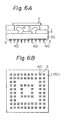
- Figure 6A is a cross-sectional view of another embodiment of a package according to the present invention.
- Figure 6B is a schematic plan view of Fig. 6A.
- Figs. 6A and 6B there are provided conductor pads 3 provided with conductor pins 40 on almost the entire back surface of the package 1.
- the semiconductor chip 5 is mounted on the base substrate 50 and the conductor pins 40 are provide on the same base substrate 50.
- this base substrate comprises a multi-layer ceramic substrate in which signal lines and plated through holes are provided for connection between the chip 5 and the conductor pin 40. Therefore, the conductor pins 40 can be provided on the entire back surface of the package 1.
- the conductor pins 40 are brazed to the conductor pads 3 as explained above.
- Such a package structure has the same effect as that explained in Figs. 4 and 5A.
- the semiconductor device of the present invention has a structure in which the outer pins, e.g., conductor pins are electrically connected to the conductor pads 9 of the circuit board 2 under a contacting condition which is different from a inserted condition.
- the outer pins provided to the package are inserted to holes of the circuit board.
- the using holes for insertion of the outer pins means a reduction of pin density and an increase of the package size.
- the present invention does not use the hole connection type but the contacting connection type which is the same as the leadless package, i.e., the chip carrier having outer pads, not pins, the conductor pins' density thereof is much higher than that of the conventional package. This means the size of the package can be small and also the density of the semiconductor device packages on the circuit board is high.
Abstract
Description
- The present invention relates to packaging of a semiconductor device, and more particularly to an assembly of a package connected to a circuit board.
- In recent years, leadless packages also known as chip carriers, have come into increasing use for accommodating integrated circuits (IC), large-scale integrated circuits (LSI), and similar devices. Like conventional packages with outer leads, leadless packages accommodate an IC chip and outer contact pads of the leadless package are electrically connected to a circuit board by soldering. They therefore can be used in popular assembly processes. At the same time, the provision of the contact pads as the conducting elements in place of outer leads enables a more compact structure. Therefore, such packages can be mounted at a higher density on a circuit board, compared with other packages. This highly prized feature has resulted in leadless packages being widely used in a broad range of fields.
- There is, however, a problem with mounting the package directly on to the circuit board by a rigid soldering technique in that the electrical connections tend to fracture during heating and cooling. Normally, the package, substrate, and circuit board are formed from different materials having different coefficients of thermal expansion. During the heating required to accomplish the mounting and during normal operating conditions, the package, substrate, and the circuit board contract and expand at different rates, thereby generating stresses. These stresses can fracture the package, substrate, circuit board, or the soldered connection. This problem is compounded the greater the size of the devices on the circuit board. Such breakage, of course, has a fatal effect on the operation of the electronic circuits formed on the circuit board.
- According to this invention a semiconductor device assembly comprising:
- a semiconductor chip;
- a package in which the semiconductor chip is contained and mounted;
- a plurality of conductor pads provided on the outer surface of the package and electrically connected to the chip; and,
- a circuit board having a plurality of contact pads in locations corresponding to those of the conductor pads
- also includes a plurality of conductor pins fixed to the conductor pads and projecting substantially normally away from them, the conductor pins also being fixed to the contact pads electrically and mechanically to connect the package to the circuit board, whilst, at the same time accommodating differing thermal expansion of the package and the circuit board.
- The present invention also embraces a semiconductor device package for use in such an assembly comprising a semiconductor chip;
- a package in which the semiconductor chip is mounted; and,
- a plurality of conductor pads provided on the outer surface of the package,
- the package also including a plurality of conductor pins fixed to the conductor pads and projecting substantially normally away from them.
- Particular embodiments of semiconductor devices in accordance with this invention will now be described and contrasted with the prior art with reference to the accompanying drawings; in which:-
- Figure 1A is a partially sectioned side elevation of a conventional semiconductor device assembly;
- Figure 1B is an underplan of the conventional semiconductor package;
- Figure 2 is a side elevation of another conventional semiconductor device;
- Figure 3 is an exploded cross-section through a further conventional semiconductor device assembly;
- Figure 4 is a partly setioned side elevation of an embodiment of the present invention;
- Figure 5A is a partly sectioned side elevation of an embodiment of a semiconductor device assembly according to the present invention;
- Figure 5B is a cross-section to a larger scale of the connecting portions of the embodiment in accordance with this invention;
- Figure 6A is a partly sectioned side elevation of another embodiment according to the present invention; and,
- Figure 6B is an underplan of the package shown in Figure 6A.
- Before describing the preferred embodiments of the invention, an explanation will be made of the prior art for comparative purposes with reference to Figures lA to 3.
- Figure 1A is a partial cross-sectional view of a conventional semiconductor device assembly comprising a plurality of LSI's in packages and a circuit board.
- In Figure lA, there is a
package 1 electrically connected to a circuit board 2 throughconductor pads 3 andsolder 4.Reference numerals - There are a plurality of
conductor pads 3, for example, from 200 to 300, in the LSI. Connectingelectrodes 9 provided on the circuit board 2 are connected to theconductor pads 3 of thepackage 1 by thesolder 4, which has a thickness of about 50 µm. - When thermal shock is generated during the operation of the circuit, the soldered connecting portion sometimes breaks, e.g., the solder cracks and falls off or the connecting
electrode 9 are separated from the circuit board 2. The main reason for the heat-induced breakage is that the circuit board 2 is made of epoxy, polyimide, or other organic resins, which have a large thermal expansion coefficient, while thepackage 1 is made of ceramic, which has a small thermal expansion coefficient. Thus, the stress is given to the soldered connecting portion. - The circuit board 2 can be made of ceramic too, which would eliminate the stress problem of thus breakage of the soldered connecting portions, however ceramic has high dielectric constant and would thus slow down the operation of the electronic circuits. Thus, ceramic is unsuitable for circuit boards except in special cases.
- Figure 2 is a schematic view of a semiconductor device disclosed in IBM Technical Disclosure Bulletin vol. 18 No. 5 October 1975 PP 1379-1380.
- In Fig. 2, a
semiconductor device 17 is mounted on and connected to acarrier 15 provided withpins 16 through a plurality offlexible strands 18. The bottom ends of theflexible strands 18 are aligned withsolder mounds 19 on the top surface of thecarrier 15. The top ends of theflexible strands 18 are connected to solder mounds 20 on thesemiconductor device 17. - In this structure, the flexible strands form an electrical connection between the package and substrate. They are typically formed of thin copper wire. The strands are not, however, strong enough to be used advantageously as connecting portions between a package and circuit board. That is, since the strands are flexible, it becomes very complicated to assemble these
flexible strands 18 to thesemiconductor device 17 and thecarrier 15. In fact, this publication discloses a complicated method where anspecial interposer 16 is used for assembling. And also, theflexible strands 18 have a demerit in which, the structure is weak about the kinetic intensity against the pressure 21 (horizontal direction). - Figure 3 shows a disclosed conventional semiconductor device assembly disclosed in IBM Technical Disclosure Bullet vol. 19 No. 4 September 1976 PP 1207-1271.
- As shown in Fig. 3, a multilayer
ceramic substrate 25 withsemiconductor devices 17 mounted on the top surface is provided with a plurality ofpads 26 on the bottom surface. The multilayerceramic substrate 25 is electrically connected to a multilayer laminated input/output distribution board 27 provided withpads 28 and wiring 29 through a spring-biasedpin contact element 30 which includes a pair of slidably mountedpins 31 biased by a suitable spring 32 including a flange 33. The spring-biasedpin contact element 30 is mounted in a socket board 35 provided with asuitable aperture 36. A socket retainer board 37 is disposed over theelement 30 retaining it in position. Such a structure is not suitable for high density integration. The reason for that is that the socket board 35 must include theapertures 36 to accommodate the flanges 33. Making apertures for connecting pins and flanges means a reduction of pin density and an increase of the package size of the semiconductor device. - Figure 4 is a cross-sectional view of an embodiment of a package according to the present invention.
- In Fig. 4, a
package 1 is provided withconductor pins 40 throughconductor pads 3. Theconductor pins 40 are brazed to theconductor pads 3. Elements the same as in Fig. lA are denoted by the same reference numerals. - The package of Fig. 4 is soldered through the conductor pins 40 to
pads 9 provided on the top surface of the circuit board 2, as shown in Fig. 5A. - Figure 5B is an enlarged cross-sectional view of the connecting portions shown in Fig. 5A.
- In Fig. 5B, the
package 1 and the circuit board 2 haveconductor pads conductor pads 3 of thepackage 1 are formed as a metallized layer during sintering of the ceramic substrate and are plated with nickel. The conductor pins 40 are brazed to the metallizedconductor pads 3 withsilver alloy 41, such as of silver and copper, at a brazing temperature of 800°C to.850°C, the conductor pins 40 are fixed to the surface of the conductor pins 3 under the substantially vertical contactcondition conductor pads 3. Then, the surface of theconductor pads 3, conductor pins 40, andsilver alloy 41 are generally plated with nickel and gold, i.e., two plating layers. The another conductor pins 3' is provided on the other size of the package. These are used for test pins. - In mounting the
package 1 on the circuit board 2, the conductor pins 40 are soldered toconductor pads 9 of the circuit board 2 usingsolder 42 at a well-known soldering temperature of, for example, 150°C to 200°C. Theconductor pads 9 consist of a copper layer plated with soft solder consisting of, for example, lead or tin alloy, and the like. - If the
conductor pads 3 are 0.2 to 0.25 mm square, conductor pins 40 having a length of 0.5 to 1.5 mm and a diameter of 0.1 to 0.2 mm are preferably used. - The conductor pins are preferably made of a lowthernal expansion coefficient alloysuch as Iron-Nickel alloy, Iron-Nickel-Cobalt alloy, tungsten, molybdenum, or copper alloy which have strengths of 200g to 400g/Iron-Nickel-Cobalt alloy Pin.
- The structure shown in Fig. 4 has the merits that when the package is electrically connected to the circuit board or the like, the thermal stress generated during the operation of the assembly can be absorbed by the conductor pins 40 since they act as buffers of thermal stress. Thus, fractures of connecting portions can be prevented.
- Figure 6A is a cross-sectional view of another embodiment of a package according to the present invention. Figure 6B is a schematic plan view of Fig. 6A.
- As illustrated in Figs. 6A and 6B, there are provided
conductor pads 3 provided with conductor pins 40 on almost the entire back surface of thepackage 1. In this embodiment, thesemiconductor chip 5 is mounted on thebase substrate 50 and the conductor pins 40 are provide on thesame base substrate 50. Furthermore, this base substrate comprises a multi-layer ceramic substrate in which signal lines and plated through holes are provided for connection between thechip 5 and theconductor pin 40. Therefore, the conductor pins 40 can be provided on the entire back surface of thepackage 1. The conductor pins 40 are brazed to theconductor pads 3 as explained above. Such a package structure has the same effect as that explained in Figs. 4 and 5A. - Furthermore, the semiconductor device of the present invention has a structure in which the outer pins, e.g., conductor pins are electrically connected to the
conductor pads 9 of the circuit board 2 under a contacting condition which is different from a inserted condition. Normally, the outer pins provided to the package are inserted to holes of the circuit board. However, the using holes for insertion of the outer pins means a reduction of pin density and an increase of the package size. - Since the present invention does not use the hole connection type but the contacting connection type which is the same as the leadless package, i.e., the chip carrier having outer pads, not pins, the conductor pins' density thereof is much higher than that of the conventional package. This means the size of the package can be small and also the density of the semiconductor device packages on the circuit board is high.
Claims (10)
Applications Claiming Priority (2)
| Application Number | Priority Date | Filing Date | Title |
|---|---|---|---|
| JP25858/83 | 1983-02-17 | ||
| JP58025858A JPS59151443A (en) | 1983-02-17 | 1983-02-17 | Semiconductor device |
Publications (3)
| Publication Number | Publication Date |
|---|---|
| EP0117111A2 true EP0117111A2 (en) | 1984-08-29 |
| EP0117111A3 EP0117111A3 (en) | 1986-03-26 |
| EP0117111B1 EP0117111B1 (en) | 1991-05-08 |
Family
ID=12177513
Family Applications (1)
| Application Number | Title | Priority Date | Filing Date |
|---|---|---|---|
| EP84300895A Expired - Lifetime EP0117111B1 (en) | 1983-02-17 | 1984-02-13 | Semiconductor device assembly |
Country Status (4)
| Country | Link |
|---|---|
| US (1) | US4724472A (en) |
| EP (1) | EP0117111B1 (en) |
| JP (1) | JPS59151443A (en) |
| DE (1) | DE3484540D1 (en) |
Cited By (5)
| Publication number | Priority date | Publication date | Assignee | Title |
|---|---|---|---|---|
| FR2622741A1 (en) * | 1987-11-04 | 1989-05-05 | Nec Corp | Structure for connecting substrates with different thermal expansion coefficients |
| EP0337686A2 (en) * | 1988-04-12 | 1989-10-18 | Hitachi, Ltd. | Semiconductor chip module |
| EP0346061A2 (en) * | 1988-06-08 | 1989-12-13 | Fujitsu Limited | Integrated circuit device having an improved package structure |
| EP0498412A1 (en) * | 1991-02-08 | 1992-08-12 | Kabushiki Kaisha Toshiba | Semiconductor device including a package having a plurality of bumps arranged in a grid form as external terminals |
| EP0646963A1 (en) * | 1993-09-30 | 1995-04-05 | Kabushiki Kaisha Toshiba | Multi-chip module and manufacturing method thereof |
Families Citing this family (35)
| Publication number | Priority date | Publication date | Assignee | Title |
|---|---|---|---|---|
| CN1003524B (en) * | 1985-10-14 | 1989-03-08 | 株式会社日立制作所 | Electroless gold plating solution |
| JPS62287658A (en) * | 1986-06-06 | 1987-12-14 | Hitachi Ltd | Ceramic multilayered circuit board and semiconductor module |
| JPS63271944A (en) * | 1987-04-28 | 1988-11-09 | Sumitomo Electric Ind Ltd | Semiconductor device |
| FR2621173B1 (en) * | 1987-09-29 | 1989-12-08 | Bull Sa | HIGH DENSITY INTEGRATED CIRCUIT BOX |
| JPH01217993A (en) * | 1988-02-26 | 1989-08-31 | Hitachi Ltd | Semiconductor device |
| JP2509285B2 (en) * | 1988-03-18 | 1996-06-19 | 富士通株式会社 | Semiconductor device testing method |
| JPH0756887B2 (en) * | 1988-04-04 | 1995-06-14 | 株式会社日立製作所 | Semiconductor package and computer using the same |
| US5170245A (en) * | 1988-06-15 | 1992-12-08 | International Business Machines Corp. | Semiconductor device having metallic interconnects formed by grit blasting |
| US5046971A (en) * | 1988-12-14 | 1991-09-10 | Olin Corporation | Terminal pins for flexible circuits |
| JPH0363944U (en) * | 1989-10-26 | 1991-06-21 | ||
| JPH0741162Y2 (en) * | 1989-10-26 | 1995-09-20 | 京セラ株式会社 | Package for storing semiconductor devices |
| EP0463758A1 (en) * | 1990-06-22 | 1992-01-02 | Digital Equipment Corporation | Hollow chip package and method of manufacture |
| US5107328A (en) * | 1991-02-13 | 1992-04-21 | Micron Technology, Inc. | Packaging means for a semiconductor die having particular shelf structure |
| US5379191A (en) * | 1991-02-26 | 1995-01-03 | Microelectronics And Computer Technology Corporation | Compact adapter package providing peripheral to area translation for an integrated circuit chip |
| US5314003A (en) * | 1991-12-24 | 1994-05-24 | Microelectronics And Computer Technology Corporation | Three-dimensional metal fabrication using a laser |
| US5483421A (en) * | 1992-03-09 | 1996-01-09 | International Business Machines Corporation | IC chip attachment |
| US5324892A (en) * | 1992-08-07 | 1994-06-28 | International Business Machines Corporation | Method of fabricating an electronic interconnection |
| US5859470A (en) * | 1992-11-12 | 1999-01-12 | International Business Machines Corporation | Interconnection of a carrier substrate and a semiconductor device |
| JP3115155B2 (en) * | 1993-05-28 | 2000-12-04 | 株式会社東芝 | Semiconductor device and manufacturing method thereof |
| US5490040A (en) * | 1993-12-22 | 1996-02-06 | International Business Machines Corporation | Surface mount chip package having an array of solder ball contacts arranged in a circle and conductive pin contacts arranged outside the circular array |
| US5548486A (en) * | 1994-01-21 | 1996-08-20 | International Business Machines Corporation | Pinned module |
| JPH07221104A (en) * | 1994-01-28 | 1995-08-18 | Fujitsu Ltd | Semiconductor device manufacture thereof and mask for forming electrode pin and testing wherein the mask for forming electrode pin is used |
| US5541449A (en) * | 1994-03-11 | 1996-07-30 | The Panda Project | Semiconductor chip carrier affording a high-density external interface |
| JP2573809B2 (en) * | 1994-09-29 | 1997-01-22 | 九州日本電気株式会社 | Multi-chip module with built-in electronic components |
| JP3004578B2 (en) * | 1995-05-12 | 2000-01-31 | 財団法人工業技術研究院 | Integrated Circuit Package Consisting of Multi-Heat Conductors for Enhanced Heat Dissipation and Caps Around the Edge for Improved Package Integrity and Reliability |
| US5878483A (en) * | 1995-06-01 | 1999-03-09 | International Business Machines Corporation | Hammer for forming bulges in an array of compliant pin blanks |
| US5675183A (en) * | 1995-07-12 | 1997-10-07 | Dell Usa Lp | Hybrid multichip module and methods of fabricating same |
| US5991160A (en) * | 1995-12-27 | 1999-11-23 | Infineon Technologies Corporation | Surface mount LED alphanumeric display |
| US5889326A (en) * | 1996-02-27 | 1999-03-30 | Nec Corporation | Structure for bonding semiconductor device to substrate |
| US6141869A (en) * | 1998-10-26 | 2000-11-07 | Silicon Bandwidth, Inc. | Apparatus for and method of manufacturing a semiconductor die carrier |
| US6543674B2 (en) | 2001-02-06 | 2003-04-08 | Fujitsu Limited | Multilayer interconnection and method |
| KR100416838B1 (en) * | 2001-06-29 | 2004-02-05 | 주식회사 하이닉스반도체 | Package device of semiconductor and method for manufacturing same |
| US7015869B2 (en) | 2002-11-18 | 2006-03-21 | Visteon Global Technologies, Inc. | High frequency antenna disposed on the surface of a three dimensional substrate |
| US7086868B2 (en) * | 2003-12-09 | 2006-08-08 | Xytrans, Inc. | Board-to-board connector |
| US20160343646A1 (en) * | 2015-05-21 | 2016-11-24 | Qualcomm Incorporated | High aspect ratio interconnect for wafer level package (wlp) and integrated circuit (ic) package |
Citations (4)
| Publication number | Priority date | Publication date | Assignee | Title |
|---|---|---|---|---|
| DE1234817B (en) * | 1963-12-27 | 1967-02-23 | Ibm | Micro-connection for microcircuit elements to be applied to a microelectronic circuit card and a method for their production |
| US3561107A (en) * | 1964-12-02 | 1971-02-09 | Corning Glass Works | Semiconductor process for joining a transistor chip to a printed circuit |
| EP0027017A1 (en) * | 1979-10-04 | 1981-04-15 | Fujitsu Limited | Integrated circuit package |
| US4338621A (en) * | 1980-02-04 | 1982-07-06 | Burroughs Corporation | Hermetic integrated circuit package for high density high power applications |
Family Cites Families (2)
| Publication number | Priority date | Publication date | Assignee | Title |
|---|---|---|---|---|
| JPS5559746A (en) * | 1978-10-27 | 1980-05-06 | Hitachi Ltd | Semiconductor device and its mounting circuit device |
| JPS57181144A (en) * | 1981-05-01 | 1982-11-08 | Toshiba Corp | Semiconductor device |
-
1983
- 1983-02-17 JP JP58025858A patent/JPS59151443A/en active Pending
-
1984
- 1984-02-13 EP EP84300895A patent/EP0117111B1/en not_active Expired - Lifetime
- 1984-02-13 DE DE8484300895T patent/DE3484540D1/en not_active Expired - Fee Related
-
1987
- 1987-01-14 US US07/006,347 patent/US4724472A/en not_active Expired - Lifetime
Patent Citations (4)
| Publication number | Priority date | Publication date | Assignee | Title |
|---|---|---|---|---|
| DE1234817B (en) * | 1963-12-27 | 1967-02-23 | Ibm | Micro-connection for microcircuit elements to be applied to a microelectronic circuit card and a method for their production |
| US3561107A (en) * | 1964-12-02 | 1971-02-09 | Corning Glass Works | Semiconductor process for joining a transistor chip to a printed circuit |
| EP0027017A1 (en) * | 1979-10-04 | 1981-04-15 | Fujitsu Limited | Integrated circuit package |
| US4338621A (en) * | 1980-02-04 | 1982-07-06 | Burroughs Corporation | Hermetic integrated circuit package for high density high power applications |
Non-Patent Citations (3)
| Title |
|---|
| IBM TECHNICAL DISCLOSURE BULLETIN, vol. 18, no. 5, October 1975, pages 1379-1380, Armonk, US; P.GELDERMANS: "Flexible solder connection and method of fabricating" * |
| Integrated Circuits: Materials, Devices and Fabrication, W.C. Till & J.T. Luxon, Prentice-Hall, New Jersey, U.S.A., 1982, Section 13.2, page 365, second paragraph * |
| PATENTS ABSTRACTS OF JAPAN, vol. 7, no. 27 (E-156)[1172], 3rd February 1983; & JP-A-57 181 144 (TOKYO SHIBAURA DENKI K.K.) 08-11-1982 * |
Cited By (8)
| Publication number | Priority date | Publication date | Assignee | Title |
|---|---|---|---|---|
| FR2622741A1 (en) * | 1987-11-04 | 1989-05-05 | Nec Corp | Structure for connecting substrates with different thermal expansion coefficients |
| EP0337686A2 (en) * | 1988-04-12 | 1989-10-18 | Hitachi, Ltd. | Semiconductor chip module |
| EP0337686A3 (en) * | 1988-04-12 | 1991-05-22 | Hitachi, Ltd. | Semiconductor chip module |
| EP0346061A2 (en) * | 1988-06-08 | 1989-12-13 | Fujitsu Limited | Integrated circuit device having an improved package structure |
| EP0346061A3 (en) * | 1988-06-08 | 1991-04-03 | Fujitsu Limited | Integrated circuit device having an improved package structure |
| EP0498412A1 (en) * | 1991-02-08 | 1992-08-12 | Kabushiki Kaisha Toshiba | Semiconductor device including a package having a plurality of bumps arranged in a grid form as external terminals |
| US5191511A (en) * | 1991-02-08 | 1993-03-02 | Kabushiki Kaisha Toshiba | Semiconductor device including a package having a plurality of bumps arranged in a grid form as external terminals |
| EP0646963A1 (en) * | 1993-09-30 | 1995-04-05 | Kabushiki Kaisha Toshiba | Multi-chip module and manufacturing method thereof |
Also Published As
| Publication number | Publication date |
|---|---|
| US4724472A (en) | 1988-02-09 |
| DE3484540D1 (en) | 1991-06-13 |
| JPS59151443A (en) | 1984-08-29 |
| EP0117111A3 (en) | 1986-03-26 |
| EP0117111B1 (en) | 1991-05-08 |
Similar Documents
| Publication | Publication Date | Title |
|---|---|---|
| EP0117111B1 (en) | Semiconductor device assembly | |
| KR100231366B1 (en) | Semiconductor package stack module and method of producing the same | |
| US5386341A (en) | Flexible substrate folded in a U-shape with a rigidizer plate located in the notch of the U-shape | |
| US6084777A (en) | Ball grid array package | |
| US5942795A (en) | Leaded substrate carrier for integrated circuit device and leaded substrate carrier device assembly | |
| US4825284A (en) | Semiconductor resin package structure | |
| US6573609B2 (en) | Microelectronic component with rigid interposer | |
| US5757071A (en) | C4 substrate contact pad which has a layer of Ni-B plating | |
| US6208025B1 (en) | Microelectronic component with rigid interposer | |
| US5668405A (en) | Semiconductor device with a film carrier tape | |
| US7180170B2 (en) | Lead-free integrated circuit package structure | |
| US6617695B1 (en) | Semiconductor device and semiconductor module using the same | |
| US20070095563A1 (en) | Circuit board having deformation interrupting section and circuit board forming method | |
| KR20010072971A (en) | Through hole bump contact | |
| JPH07202378A (en) | Packaged electron hardware unit | |
| US5661337A (en) | Technique for improving bonding strength of leadframe to substrate in semiconductor IC chip packages | |
| US6441486B1 (en) | BGA substrate via structure | |
| US6054652A (en) | Thin-film multi-layer substrate and electronic device | |
| EP1065719A2 (en) | Power semiconductor mounting package containing ball grid array | |
| US4731700A (en) | Semiconductor connection and crossover apparatus | |
| US6351389B1 (en) | Device and method for packaging an electronic device | |
| JP2606603B2 (en) | Semiconductor device, its manufacturing method and its mounting inspection method | |
| US20050073059A1 (en) | Integrated circuit with dual electrical attachment PAD configuration | |
| US6747352B1 (en) | Integrated circuit having multiple power/ground connections to a single external terminal | |
| JPH10189815A (en) | Mounting structure for semiconductor element mounting substrate |
Legal Events
| Date | Code | Title | Description |
|---|---|---|---|
| PUAI | Public reference made under article 153(3) epc to a published international application that has entered the european phase |
Free format text: ORIGINAL CODE: 0009012 |
|
| AK | Designated contracting states |
Designated state(s): DE FR GB |
|
| PUAL | Search report despatched |
Free format text: ORIGINAL CODE: 0009013 |
|
| AK | Designated contracting states |
Kind code of ref document: A3 Designated state(s): DE FR GB |
|
| 17P | Request for examination filed |
Effective date: 19860819 |
|
| 17Q | First examination report despatched |
Effective date: 19880125 |
|
| GRAA | (expected) grant |
Free format text: ORIGINAL CODE: 0009210 |
|
| AK | Designated contracting states |
Kind code of ref document: B1 Designated state(s): DE FR GB |
|
| REF | Corresponds to: |
Ref document number: 3484540 Country of ref document: DE Date of ref document: 19910613 |
|
| ET | Fr: translation filed | ||
| PLBE | No opposition filed within time limit |
Free format text: ORIGINAL CODE: 0009261 |
|
| STAA | Information on the status of an ep patent application or granted ep patent |
Free format text: STATUS: NO OPPOSITION FILED WITHIN TIME LIMIT |
|
| 26N | No opposition filed | ||
| PGFP | Annual fee paid to national office [announced via postgrant information from national office to epo] |
Ref country code: FR Payment date: 19960125 Year of fee payment: 13 |
|
| PGFP | Annual fee paid to national office [announced via postgrant information from national office to epo] |
Ref country code: DE Payment date: 19960215 Year of fee payment: 13 |
|
| PG25 | Lapsed in a contracting state [announced via postgrant information from national office to epo] |
Ref country code: FR Effective date: 19971030 |
|
| PG25 | Lapsed in a contracting state [announced via postgrant information from national office to epo] |
Ref country code: DE Effective date: 19971101 |
|
| REG | Reference to a national code |
Ref country code: FR Ref legal event code: ST |
|
| PGFP | Annual fee paid to national office [announced via postgrant information from national office to epo] |
Ref country code: GB Payment date: 20010207 Year of fee payment: 18 |
|
| REG | Reference to a national code |
Ref country code: GB Ref legal event code: IF02 |
|
| PG25 | Lapsed in a contracting state [announced via postgrant information from national office to epo] |
Ref country code: GB Free format text: LAPSE BECAUSE OF NON-PAYMENT OF DUE FEES Effective date: 20020213 |
|
| GBPC | Gb: european patent ceased through non-payment of renewal fee |
Effective date: 20020213 |