EP0131422A1 - Adjustable monolithic ceramic capacitor - Google Patents
Adjustable monolithic ceramic capacitor Download PDFInfo
- Publication number
- EP0131422A1 EP0131422A1 EP84304541A EP84304541A EP0131422A1 EP 0131422 A1 EP0131422 A1 EP 0131422A1 EP 84304541 A EP84304541 A EP 84304541A EP 84304541 A EP84304541 A EP 84304541A EP 0131422 A1 EP0131422 A1 EP 0131422A1
- Authority
- EP
- European Patent Office
- Prior art keywords
- electrodes
- main
- capacitor
- auxiliary
- ceramic
- Prior art date
- Legal status (The legal status is an assumption and is not a legal conclusion. Google has not performed a legal analysis and makes no representation as to the accuracy of the status listed.)
- Granted
Links
Images
Classifications
-
- H—ELECTRICITY
- H01—ELECTRIC ELEMENTS
- H01G—CAPACITORS; CAPACITORS, RECTIFIERS, DETECTORS, SWITCHING DEVICES OR LIGHT-SENSITIVE DEVICES, OF THE ELECTROLYTIC TYPE
- H01G4/00—Fixed capacitors; Processes of their manufacture
- H01G4/002—Details
- H01G4/255—Means for correcting the capacitance value
Definitions
- This invention relates to an adjustable monolithic ceramic capacitors having a pair of main electrodes extending to opposite ends of a very small capacitor body, and more particularly to such capacitors having auxiliary electrodes between the main electrodes.
- Monolithic ceramic capacitors typically consist of a dielectric ceramic body having two groups of main electrodes buried therein. One group extends to a side of the body and the other group to another side for termination and electrical access.
- the electrical capacity so obtained in the capacitor is a function.of many variables of which the major are dielectric thickness between adjacent electrodes, dielectric constant (K) of the ceramic, and registration between adjacent electrodes. It is not unusual for capacity values of a production lot of monolithic capacitors to vary by 40%.
- Another prior art technique for adjusting capacity includes providing several auxiliary electrodes that extend to yet another surface of the ceramic body. These auxiliary electrodes are buried between two main electrodes that extend to the same main terminal of the capacitor and, when connected externally to the other main terminal of the capacitor, the capacitance increases.
- a feature of this invention is the provision of an alternative method for adjusting the capacitance value of a monolithic ceramic capacitor. Another feature is the provision of an improved adjustable monolithic ceramic capacitor applicable to capacitors of very small size.
- the present invention provides a monolithic ceramic capacitor comprising a ceramic body characterised by at least two main sheet electrodes buried in said body and spaced by a central layer of said ceramic body, each of said main electrodes extending to one of opposite ends of said body, respectively, said two main electrodes having a region of overlap that is spaced from said body ends and from the two side edges of said body, and at least two spaced auxiliary sheet electrodes buried in said central ceramic layer and extending to at least one of said side edges, whereby the capacitance between said two main electrodes is increased when one of said auxiliary electrodes is electrically connected to either of said main electrodes.
- the monolithic ceramic capacitor of this invention has two main sheet electrodes buried in a dielectric ceramic body.
- the two main electrodes are spaced apart by a central layer of the body.
- the two main electrodes extend, respectively, to two opposite ends of the body and overlap each other in a region that is spaced from the two opposite ends, as well as from the two side edges of the body.
- the area of overlap can be substantially less than the maximum possible area and preferably less than 33%.
- At least two spaced apart auxiliary sheet electrodes are buried in the central ceramic layer between the main electrodes and extend to one or one another of the aforementioned side edges.
- the capacitance measured between the main electrodes at the opposite body ends, increases when any one of the auxiliary electrodes is connected to either one of the main electrodes.
- This invention is especially concerned with small monolithic ceramic capacitors wherein the active overlap region is no more than one third the maximum possible area represented by the total area of a main-electrode within the ceramic body.
- the ceramic capacitor illustrated in the Figures has a dielectric ceramic body 10 having buried therein two main electrodes 12 and 14. Electrode 12 lies in plane X - Y and has the shape of a T. Electrodes 12 and 14 overlap in a central region of body 10 where essentially all of the electrical capacity between them is developed. A pair of auxiliary electrodes 16 and 18 is buried in the dielectric ceramic in the above-hoted overlap region between the two main electrodes 12 and 14.
- Body 10 is 0.080 inch (2.03 mm) long (in the X-direction) and 0.050 inch (1.27 mm) wide (in the Y-direction).
- the active-capacity overlap area of main electrodes 12 and 14 is thus a small part of the total area of the X - Y plane that lies within body 10, namely about 18%, so that adequate spaces are provided between electrodes (e.g. between 16 and 18, and between 18 and 14) to avoid inadvertent shorting when applying external terminations 20 and 22.
- the capacity between main electrodes 12 and 14 is about 3.4 pf, with the auxiliary electrodes 16 and 18 disconnected and "floating" electrically (absent such connections as 20b and 22b).
- auxiliary electrodes 16 and 18 are spaced from main electrode 12 by about 1 mil (0.025 mm) and are spaced from main electrode 14 by about 2 mils (0.051 mm). If either auxiliary electrode 16 or 18 is connected to main electrode 14, the capacity as seen between terminations 20 and 22 increases from 3.4 pf to 4.0 pf. On the other hand if either auxiliary electrode 16 or 18 is connected to main electrode 12, the capacity between terminations 20 and 22 increases from 3.4 pf to 5.7 pf.
- Table below The possible capacity values obtainable by permuting the auxiliary electrode connections are shown in the Table below:
- Capacitors of this invention may be made by any of the methods well-known to the monolithic ceramic capacitor art. Briefly, a slurry of ceramic powder is formed in a liquid medium consisting of xylene as a vehicle, methylmethacrylate as a binder, and a surfactant such as lecithin. Successive coatings of the ceramic slurry are deposited on a substrate, each coating being dried before depositing the next. On some of the dried coatings a pattern of a palladium-containing electroding ink is screen printed. This stack is then fired to maturity at from 1000 to 1400°C in air.
- the side edges and the ends to which electrodes extend may be abraded to expose the electrodes more fully, and a silver containing paint is applied to those ends and edges.
- the body is then fired at about 760°C to cure the silver paint and form conducting terminations 20a, 20b, 22a and 22b that each contacts certain of the buried electrodes 12, 16, 14 and 18, respectively.
- terminations In the application of terminations to the body 10, one or both, or neither of termination portions 20b and 22b may be used. Such election may be made for a production batch of capacitor bodies having a tight spread of capacities.
- terminations may be fully applied as shown in Figure 2 and thereafter portions of one or both terminations 20 and 22 may be severed to cause one or both auxiliary electrodes 18 and 16 to float electrically, thus eliminating their influence on the capacitance value. For example, to disconnect auxiliary electrode 18, a center region of termination portion 22b may be severed.
- termination portions 20a and 22a are applied to all the bodies. These end terminated bodies can then be tested and classified by capacity into a number of groups. For each group, termination portions 20b and 22b are applied as needed to make all capacities close in value to a desired nominal capacity.
Abstract
Description
- This invention relates to an adjustable monolithic ceramic capacitors having a pair of main electrodes extending to opposite ends of a very small capacitor body, and more particularly to such capacitors having auxiliary electrodes between the main electrodes.
- Monolithic ceramic capacitors typically consist of a dielectric ceramic body having two groups of main electrodes buried therein. One group extends to a side of the body and the other group to another side for termination and electrical access. The electrical capacity so obtained in the capacitor is a function.of many variables of which the major are dielectric thickness between adjacent electrodes, dielectric constant (K) of the ceramic, and registration between adjacent electrodes. It is not unusual for capacity values of a production lot of monolithic capacitors to vary by 40%.
- Misregistration between adjacent electrodes can be eliminated as a source of variation in capacitance by designing the electrode patterns so that there is a constant predetermined area of overlap between adjacent electrodes, as is described in my patent US 3,896,354 issued July 22, 1975.
- Also, when tighter capacitance tolerances are desired than obtainable in a given process, it is known in the prior art to abrade a cavity into the body, thereby removing central portions of some of the electrodes and surrounding ceramic to thereby reduce the capacity to the desired value. Such a technique is described by Hatch in US 3,456,170 issued July 15, 1969. However, the abrading technique is not practical for use with very small capacitors wherein the electrode overlap area is small compared to that of the capacitor body profile.
- Another prior art technique for adjusting capacity includes providing several auxiliary electrodes that extend to yet another surface of the ceramic body. These auxiliary electrodes are buried between two main electrodes that extend to the same main terminal of the capacitor and, when connected externally to the other main terminal of the capacitor, the capacitance increases.
- A feature of this invention is the provision of an alternative method for adjusting the capacitance value of a monolithic ceramic capacitor. Another feature is the provision of an improved adjustable monolithic ceramic capacitor applicable to capacitors of very small size.
- The present invention provides a monolithic ceramic capacitor comprising a ceramic body characterised by at least two main sheet electrodes buried in said body and spaced by a central layer of said ceramic body, each of said main electrodes extending to one of opposite ends of said body, respectively, said two main electrodes having a region of overlap that is spaced from said body ends and from the two side edges of said body, and at least two spaced auxiliary sheet electrodes buried in said central ceramic layer and extending to at least one of said side edges, whereby the capacitance between said two main electrodes is increased when one of said auxiliary electrodes is electrically connected to either of said main electrodes. In a drawing which illustrates embodiments of
- the invention:
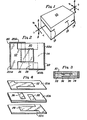
- Figure 1 shows a perspective view of an adjustable monolithic ceramic capacitor;
- Figure 2 shows a top sectional view of the capacitor of Figure 1 taken in plane X - Y as seen in
direction 2; - Figure 3 shows a side sectional view of the capacitor of Figure 1 taken in plane X - Z looking in direction 3; and
- Figure 4 is an exploded view of three of the ceramic layers with deposited electrodes which form the capacitor of Figure 1.
- In general, the monolithic ceramic capacitor of this invention has two main sheet electrodes buried in a dielectric ceramic body. The two main electrodes are spaced apart by a central layer of the body. The two main electrodes extend, respectively, to two opposite ends of the body and overlap each other in a region that is spaced from the two opposite ends, as well as from the two side edges of the body. Thus the area of overlap can be substantially less than the maximum possible area and preferably less than 33%. At least two spaced apart auxiliary sheet electrodes are buried in the central ceramic layer between the main electrodes and extend to one or one another of the aforementioned side edges.
- Thus the capacitance, measured between the main electrodes at the opposite body ends, increases when any one of the auxiliary electrodes is connected to either one of the main electrodes.
- This invention is especially concerned with small monolithic ceramic capacitors wherein the active overlap region is no more than one third the maximum possible area represented by the total area of a main-electrode within the ceramic body.
- The ceramic capacitor illustrated in the Figures has a dielectric
ceramic body 10 having buried therein twomain electrodes T. Electrodes body 10 where essentially all of the electrical capacity between them is developed. A pair ofauxiliary electrodes main electrodes -
Body 10 is 0.080 inch (2.03 mm) long (in the X-direction) and 0.050 inch (1.27 mm) wide (in the Y-direction). The active-capacity overlap area ofmain electrodes body 10, namely about 18%, so that adequate spaces are provided between electrodes (e.g. between 16 and 18, and between 18 and 14) to avoid inadvertent shorting when applyingexternal terminations - Using a ceramic matexial having a K of about 70, and a dielectric spacing between the
main electrodes main electrodes auxiliary electrodes - The
auxiliary electrodes main electrode 12 by about 1 mil (0.025 mm) and are spaced frommain electrode 14 by about 2 mils (0.051 mm). If eitherauxiliary electrode main electrode 14, the capacity as seen betweenterminations auxiliary electrode main electrode 12, the capacity betweenterminations 
- Capacitors of this invention may be made by any of the methods well-known to the monolithic ceramic capacitor art. Briefly, a slurry of ceramic powder is formed in a liquid medium consisting of xylene as a vehicle, methylmethacrylate as a binder, and a surfactant such as lecithin. Successive coatings of the ceramic slurry are deposited on a substrate, each coating being dried before depositing the next. On some of the dried coatings a pattern of a palladium-containing electroding ink is screen printed. This stack is then fired to maturity at from 1000 to 1400°C in air. The side edges and the ends to which electrodes extend may be abraded to expose the electrodes more fully, and a silver containing paint is applied to those ends and edges. The body is then fired at about 760°C to cure the silver paint and form conducting
terminations electrodes - In the application of terminations to the
body 10, one or both, or neither oftermination portions terminations auxiliary electrodes auxiliary electrode 18, a center region oftermination portion 22b may be severed. - As a third alternative, and in most cases the most attractive, only
termination portions termination portions
Claims (5)
Applications Claiming Priority (2)
| Application Number | Priority Date | Filing Date | Title |
|---|---|---|---|
| US06/511,416 US4466045A (en) | 1983-07-06 | 1983-07-06 | Adjustable monolithic ceramic capacitor |
| US511416 | 1983-07-06 |
Publications (2)
| Publication Number | Publication Date |
|---|---|
| EP0131422A1 true EP0131422A1 (en) | 1985-01-16 |
| EP0131422B1 EP0131422B1 (en) | 1988-05-18 |
Family
ID=24034814
Family Applications (1)
| Application Number | Title | Priority Date | Filing Date |
|---|---|---|---|
| EP84304541A Expired EP0131422B1 (en) | 1983-07-06 | 1984-07-03 | Adjustable monolithic ceramic capacitor |
Country Status (5)
| Country | Link |
|---|---|
| US (1) | US4466045A (en) |
| EP (1) | EP0131422B1 (en) |
| JP (1) | JPS6037710A (en) |
| CA (1) | CA1205534A (en) |
| DE (1) | DE3471398D1 (en) |
Families Citing this family (15)
| Publication number | Priority date | Publication date | Assignee | Title |
|---|---|---|---|---|
| GB2136206B (en) * | 1983-03-02 | 1986-10-08 | Standard Telephones Cables Ltd | Fused ceramic capacitor |
| JPS61236110A (en) * | 1985-04-11 | 1986-10-21 | 株式会社村田製作所 | Laminate ceramic capacitor |
| US4720767A (en) * | 1986-09-22 | 1988-01-19 | Avx Corporation | Internally fused variable value ceramic capacitor and circuit |
| JPS63110019U (en) * | 1987-01-10 | 1988-07-15 | ||
| JPH03215915A (en) * | 1990-01-19 | 1991-09-20 | Murata Mfg Co Ltd | Laminated capacitor |
| US5018047A (en) * | 1990-07-20 | 1991-05-21 | American Technical Ceramics Corporation | Adjustable multilayer capacitor |
| US5495387A (en) * | 1991-08-09 | 1996-02-27 | Murata Manufacturing Co., Ltd. | RC array |
| DE4231616C2 (en) * | 1992-09-22 | 1995-08-24 | Seichter Gmbh | Capacitive sensor |
| US5367430A (en) * | 1992-10-21 | 1994-11-22 | Presidio Components, Inc. | Monolithic multiple capacitor |
| US6038134A (en) * | 1996-08-26 | 2000-03-14 | Johanson Dielectrics, Inc. | Modular capacitor/inductor structure |
| US7152291B2 (en) | 2002-04-15 | 2006-12-26 | Avx Corporation | Method for forming plated terminations |
| KR100826410B1 (en) * | 2006-12-29 | 2008-04-29 | 삼성전기주식회사 | Capacitor and multi-layered board embedding the capacitor |
| DE102013110978A1 (en) * | 2013-10-02 | 2015-04-16 | Epcos Ag | Ceramic multilayer capacitor |
| KR20190116171A (en) * | 2019-09-17 | 2019-10-14 | 삼성전기주식회사 | Mutilayered electronic component |
| CN113053668B (en) * | 2021-03-09 | 2023-05-16 | 北京北方华创微电子装备有限公司 | Capacitive element |
Citations (4)
| Publication number | Priority date | Publication date | Assignee | Title |
|---|---|---|---|---|
| US3688361A (en) * | 1971-06-18 | 1972-09-05 | Gulton Ind Inc | Method of making a trimmable monolithic capacitor |
| DE2246573A1 (en) * | 1972-09-22 | 1974-04-11 | Crl Electronic Bauelemente | STACKED CAPACITOR |
| US3898541A (en) * | 1973-12-17 | 1975-08-05 | Vitramon Inc | Capacitors and method of adjustment |
| US4074340A (en) * | 1976-10-18 | 1978-02-14 | Vitramon, Incorporated | Trimmable monolithic capacitors |
Family Cites Families (1)
| Publication number | Priority date | Publication date | Assignee | Title |
|---|---|---|---|---|
| US3586933A (en) * | 1970-01-15 | 1971-06-22 | Gulton Ind Inc | Trimmable monolithic capacitor and method of making the same |
-
1983
- 1983-07-06 US US06/511,416 patent/US4466045A/en not_active Expired - Fee Related
-
1984
- 1984-06-18 CA CA000456843A patent/CA1205534A/en not_active Expired
- 1984-07-03 EP EP84304541A patent/EP0131422B1/en not_active Expired
- 1984-07-03 JP JP59136666A patent/JPS6037710A/en active Granted
- 1984-07-03 DE DE8484304541T patent/DE3471398D1/en not_active Expired
Patent Citations (4)
| Publication number | Priority date | Publication date | Assignee | Title |
|---|---|---|---|---|
| US3688361A (en) * | 1971-06-18 | 1972-09-05 | Gulton Ind Inc | Method of making a trimmable monolithic capacitor |
| DE2246573A1 (en) * | 1972-09-22 | 1974-04-11 | Crl Electronic Bauelemente | STACKED CAPACITOR |
| US3898541A (en) * | 1973-12-17 | 1975-08-05 | Vitramon Inc | Capacitors and method of adjustment |
| US4074340A (en) * | 1976-10-18 | 1978-02-14 | Vitramon, Incorporated | Trimmable monolithic capacitors |
Non-Patent Citations (1)
| Title |
|---|
| 22ND ELECTRONIC COMPONENTS CONFERENCE, 15th-17th May 1972, pages 294-297, Washington D.C., USA; R.D. McBRAYER et al.: "High energy capacitors using glass-ceramic dielectrics" * |
Also Published As
| Publication number | Publication date |
|---|---|
| EP0131422B1 (en) | 1988-05-18 |
| JPS6037710A (en) | 1985-02-27 |
| JPH0337850B2 (en) | 1991-06-06 |
| US4466045A (en) | 1984-08-14 |
| DE3471398D1 (en) | 1988-06-23 |
| CA1205534A (en) | 1986-06-03 |
Similar Documents
| Publication | Publication Date | Title |
|---|---|---|
| EP0131422A1 (en) | Adjustable monolithic ceramic capacitor | |
| US3538464A (en) | Multiple pin connector having ferrite core stacked capacitor filter | |
| US7085124B2 (en) | Multilayer capacitor | |
| CA1194949A (en) | Low cost thin film capacitor | |
| US4513350A (en) | Monolithic ceramic capacitor and method for manufacturing to predetermined capacity value | |
| US6568054B1 (en) | Method of producing a multilayer electronic part | |
| US4746557A (en) | LC composite component | |
| US4556929A (en) | Multi-layer ceramic capacitor | |
| US20040114305A1 (en) | Electric multilayer component and interference supression circuit with said component | |
| JPH07326536A (en) | Ceramic capacitor | |
| US3426257A (en) | Multiple capacitor and method of making the same | |
| US4812787A (en) | Lumped constant non-reciprocal circuit element | |
| EP0869553A3 (en) | Conductive feedthrough for a ceramic body and method of fabricating same | |
| US6476690B1 (en) | Laminated LC component with rotationally symmetric capacitor electrodes | |
| US5040093A (en) | Capacitor and method of manufacturing same | |
| US5274352A (en) | Thick film resistive element, thick film printed circuit board and thick film hybrid integrated circuit device and their production methods | |
| EP0186765A2 (en) | End termination for chip capacitor | |
| US4918417A (en) | Inductor having parallel line electrodes | |
| US4356608A (en) | Method for the manufacture of layer capacitors | |
| DE3125281A1 (en) | Electrical component combination, especially an R-C combination | |
| KR100418602B1 (en) | Chip type array electronic component | |
| JPH07142285A (en) | Multilayered ceramic capacitor and its manufacture | |
| JPH10275734A (en) | Ceramics capacitor | |
| EP0817302A2 (en) | Method of forming electrodes of a dielectric filter | |
| JPH07263278A (en) | Capacitor |
Legal Events
| Date | Code | Title | Description |
|---|---|---|---|
| PUAI | Public reference made under article 153(3) epc to a published international application that has entered the european phase |
Free format text: ORIGINAL CODE: 0009012 |
|
| AK | Designated contracting states |
Designated state(s): BE DE FR GB |
|
| 17P | Request for examination filed |
Effective date: 19850401 |
|
| 17Q | First examination report despatched |
Effective date: 19860522 |
|
| D17Q | First examination report despatched (deleted) | ||
| GRAA | (expected) grant |
Free format text: ORIGINAL CODE: 0009210 |
|
| AK | Designated contracting states |
Kind code of ref document: B1 Designated state(s): BE DE FR GB |
|
| REF | Corresponds to: |
Ref document number: 3471398 Country of ref document: DE Date of ref document: 19880623 |
|
| ET | Fr: translation filed | ||
| REG | Reference to a national code |
Ref country code: GB Ref legal event code: 746 |
|
| PLBE | No opposition filed within time limit |
Free format text: ORIGINAL CODE: 0009261 |
|
| STAA | Information on the status of an ep patent application or granted ep patent |
Free format text: STATUS: NO OPPOSITION FILED WITHIN TIME LIMIT |
|
| 26N | No opposition filed | ||
| PGFP | Annual fee paid to national office [announced via postgrant information from national office to epo] |
Ref country code: GB Payment date: 19910624 Year of fee payment: 8 |
|
| PGFP | Annual fee paid to national office [announced via postgrant information from national office to epo] |
Ref country code: FR Payment date: 19910721 Year of fee payment: 8 |
|
| PGFP | Annual fee paid to national office [announced via postgrant information from national office to epo] |
Ref country code: DE Payment date: 19910830 Year of fee payment: 8 |
|
| PGFP | Annual fee paid to national office [announced via postgrant information from national office to epo] |
Ref country code: BE Payment date: 19910904 Year of fee payment: 8 |
|
| PG25 | Lapsed in a contracting state [announced via postgrant information from national office to epo] |
Ref country code: GB Effective date: 19920703 |
|
| PG25 | Lapsed in a contracting state [announced via postgrant information from national office to epo] |
Ref country code: BE Effective date: 19920731 |
|
| BERE | Be: lapsed |
Owner name: SPRAGUE ELECTRIC CY Effective date: 19920731 |
|
| GBPC | Gb: european patent ceased through non-payment of renewal fee |
Effective date: 19920703 |
|
| PG25 | Lapsed in a contracting state [announced via postgrant information from national office to epo] |
Ref country code: FR Effective date: 19930331 |
|
| PG25 | Lapsed in a contracting state [announced via postgrant information from national office to epo] |
Ref country code: DE Effective date: 19930401 |
|
| REG | Reference to a national code |
Ref country code: FR Ref legal event code: ST |