EP0135970B1 - Receiver comprising a search tuning circuit - Google Patents
Receiver comprising a search tuning circuit Download PDFInfo
- Publication number
- EP0135970B1 EP0135970B1 EP84201321A EP84201321A EP0135970B1 EP 0135970 B1 EP0135970 B1 EP 0135970B1 EP 84201321 A EP84201321 A EP 84201321A EP 84201321 A EP84201321 A EP 84201321A EP 0135970 B1 EP0135970 B1 EP 0135970B1
- Authority
- EP
- European Patent Office
- Prior art keywords
- circuit
- tuning
- input
- reverse
- output
- Prior art date
- Legal status (The legal status is an assumption and is not a legal conclusion. Google has not performed a legal analysis and makes no representation as to the accuracy of the status listed.)
- Expired
Links
Images
Classifications
-
- H—ELECTRICITY
- H03—ELECTRONIC CIRCUITRY
- H03J—TUNING RESONANT CIRCUITS; SELECTING RESONANT CIRCUITS
- H03J7/00—Automatic frequency control; Automatic scanning over a band of frequencies
- H03J7/18—Automatic scanning over a band of frequencies
- H03J7/20—Automatic scanning over a band of frequencies where the scanning is accomplished by varying the electrical characteristics of a non-mechanically adjustable element
- H03J7/28—Automatic scanning over a band of frequencies where the scanning is accomplished by varying the electrical characteristics of a non-mechanically adjustable element using counters or frequency dividers
Definitions
- the invention relates to a receiver comprising a search tuning circuit having a forward-reverse-stop circuit whose action causes the tuning of the receiver to proceed in a given forward direction after a search tuning action has started, to reverse in response to a signal received and to stop when tuning is substantially correct, having a last-found-transmission blocking circuit to prevent the same transmission from being tuned to at a restart of a search tuning action and having a manual control circuit by means of which a tuning found by a search tuning action can be changed.
- the last-found-transmission blocking circuit is a circuit with which, during a plurality of steps after a restart of the search tuning circuit, the response to the signal from which a reverse and stop action must be derived, is suppressed.
- a tuning datum found by the search tuning circuit can be changed with the manual control circuit.
- a tuning datum obtained by this changed tuning can, if so desired, be stored in a tuning data store. This feature can be found to be often the cause that an incorrect tuning datum is stored, for example a tuning datum located outside an AFC catching range.
- a receiver of the type set forth in the opening paragraph is characterized in that the last-found-transmission blocking circuit comprises a first trigger circuit an output of which is coupled-to a reverse-reset input of the forward-reverse-stop circuit, the first trigger circuit being adapted to be set by a combination of a reverse output signal of the forward-reverse-stop circuit and a tuned-too-near signal and reset by a control element for rendering the last-found-transmission blocking circuit inoperative and by a receiving condition signal.
- the search tuning circuit tunes to the transmission found last, so that the correct tuning datum associated therewith can be found again very rapidly.
- a further development of a receiver according to the invention is characterized in that it comprises a tuned-too-far memory circuit comprising a second trigger circuit which can be set by a combination of a search tuning start signal and a tuned-too-far signal, and reset by an output signal of the first trigger and an output of which is coupled to a reverse-setting input of the forward-reverse-stop circuit.
- a receiver is characterized in that the manual control circuit is coupled to a setting input of a third trigger circuit whose resetting input is coupled to a forward-setting input of the forward-reverse-stop circuit, whilst an output of this third trigger circuit is coupled to a resetting input of the first trigger circuit via a gate circuit, a further input of which is coupled to the said control element for rendering the last-found transmission blocking circuit inoperative, then the last-found transmission blocking circuit is made inoperative after manual operation, so that no search action to the same transmission takes place when the last tuning action was a search action.
- a tuning voltage is applied to an input 1 of a section 3 of the receiver, in response to which this section 3 is tuned and, upon reception of a transmission an AFC signal is produced at an output 5 and a line synchronizing signal at an output 7.
- a line flyback signal is supplied from an output 9. It is assumed here that the receiver is a television receiver.
- the output 7 can, for example, supply a rectified AFC signal and the output 9 an AVC signal.
- the output 5 of the secion 3 is connected to an input 11 of a tuning signal generator 13, an output 15 of which applies to the input of the section 3 a tuning signal which determines the tuning of the receiver.
- This tuning signal is, for example, obtained from a digital-to-analog converter arranged at an output of a counter whose counting position can be incremented or decremented, respectively by pulses to be applied to an input 17 or 19, respectively, or whose position can be determined by tuning data stored in a tuning memory 21.
- a digital-to-analog converter arranged at an output of a counter whose counting position can be incremented or decremented, respectively by pulses to be applied to an input 17 or 19, respectively, or whose position can be determined by tuning data stored in a tuning memory 21.
- the pulses at the inputs 17 or 19, respectively of the tuning signal generator 13 are obtained from AND-gates 23 and 25, respectively, an input of which is connected to an output of a pulse generator 29, whose frequency is determined by a receiving condition signal applied to an input 31 thereof.
- the other input of the AND-gates 23 and 25, respectively is connected to an output of an OR-gate 33 and 35, respectively, an input of which is connected to a manual control circuit 37 by means of which a logic one signal can be applied to the relevant input of one of the OR-gates 33, 35 for manual tuning of the receiver.
- a further input of the OR-gate 33 and 35, respectively is connected to a forward or reverse output 39 and 41, respectively of a forward-reverse-stop circuit 43, which together with a last-found transmission blocking circuit 45 forms part of a search tuning circuit.
- This search tuning circuit can be started by applying a forward-start signal to a forward-start input 47 of the forward-reverse-stop circuit 43.
- This forward-start signal is received from an output 49 of a pulse generator 51, which produces a logic one pulse when a logic one signal is produced at its input 53 which is connected to an output of an OR-gate 55. This is the case when a search tuning start switch 57, which is connected to an input of the OR-gate 55, is closed.
- the pulse then applied to the forward-start input 47 of the forward-reverse-stop circuit 43 sets via a clock signal input 59 a first D-flip-flop 61, a D-input 63 of which is connected to a positive voltage.
- an output 65 of the D-flip-flop 61 becomes one and the output 39 of the forward-reverse-stop circuit 43 connected thereto becomes consequently also one, as a result of which the tuning of the receiver is effected in a forward direction.
- an AFC signal is produced at the output 5 of the section 3, which signal is applied to an input 67 of a threshold circuit 69 which in response thereto successively supplies a tuned-too-near or a tuned-too-far signal, respectively from an output 71 and 73, respectively.
- the signals at the outputs 7 and 9 of the section 3 of the receiver are applied to respective inputs 75 and 77 of a coincidence circuit 79 which supplies from its output 81 the receiving state signal which, when there is coincidence between the line synchronizing signals and the line flyback signals is logic one which on reception of a transmission causes the frequency of the signal produced by the pulse generator 29 to be decreased, as a result of which the search rate decreases.
- the tuned-too-far signal at the output 73 of the threshold circuit 69 which becomes zero when tuning has proceeded too far, is applied to a tuned-too-far input 83 of the forward-reverse-stop circuit 43, which is connected to a clock signal input 85 of a second D-flip-flop 87 a D-input 89 of which is connected to the output 65 of the first D-flip-flop 61. Since as described above the output 65 of the first D-flip-flop becomes logic one, an output 91 of the second D-flip-flop 87 now becomes logic one.
- the signal at this output 91 which is connected to a reset input 95 of the first D-flip-flop 61 via an OR-gate 93, now resets this first D-flip-flop 61.
- the reverse-stroke output 41 of the forward-reverse-stop circuit 43 connected to the output 91 of the second flip-flop 87 is now logic one and the forward-stroke output 39 is logic one; tuning of the receiver now proceeds in the reverse direction.
- An output 103 of the third D-flip-flop 99 now becomes logic one and via an OR-gate 105 a reset input 107 of the second D-flip-flop 87 becomes logic one causing this second D-flip-flop 87 to be reset and the tuning of the receiver to stop.
- a reset-input 109 of the third D-flip-flop 99 is connected to an output of an OR-gate 111 an input of which receives the receiving state signal from the output 81 of the coincidence circuit 79.
- the third D-flip-flop 99 which functions as a first trigger circuit, opertes as a last found-transmission-blocking circuit at a restart of the search tuning circuit as it keeps the second D-flip-flop 87 in the reset state until the receiving state signal becomes logic one again, causing the third D-flip-flop 99 to be reset and the reset signal at the reset input 107 of the second D-flip-flop 87 to disappear.
- the third D-flip-flop 99 which functions as a first trigger circuit can also be reset by applying to a second input of the OR-gate 111 a signal which may be received from an AND-gate 113 when a control element 115 is operated.
- a divide-by-two divider 117 changes state and supplies from its output 119 a logic one signal which is applied to a generator 121 which then supplies a pulse which is applied to an input of the AND-gate 113.
- the other input of the AND-gate 113 is logic one when the last tuning action of the receiver was manual tuning by means of the manual tuning circuit 37, as will be described in greater detail hereinafter.
- the third D-flip-flop 99 is reset by the output signal of the OR-gate 111 when the control element 115 is operated, as a result of which the blocking of the last-found transmission of the search tuning circuit is cancelled.
- Restarting the search tuning circuit in response to a starting pulse applied to the forward-start- input 47 of the forward-reverse-stop circuit 43 renders it possible to tune again to the last-found transmission with the aid of the search tuning circuit. Because of the presence of a tuned-too-far-memory circuit 123 this is even possible when the receiver was detuned too far towards a subsequent transmitter by the manual tuning circuit 37, as a result of which the receiver would move outside the tuning range with a good reception of the last-found transmitter, when the search tuning circuit were started in the forward direction.
- the tuned-too-far memory circuit 123 comprises a fourth D-flip-flop 125 which functions as a second trigger circuit and a clock signal input 127- of which receives the starting signal from the output 49 of the pulse generator 51 and a D-input 129 receives the tuned-too-far signal from the output 73 of the threshold circuit 69.
- An output 131 of the fourth D-flip-flop 125 then becomes logic one, which also holds for a set-input 133 of the second D-flip-flop 876 connected thereto, which creates the reverse stroke state of the forward-reverse-stop circuit 43 and the search tuning circuit yet tunes to the last-found transmission.
- a reset input 135 of the fourth D-flip-flop 125 is connected to the output of the OR-gate 105 so that also the fourth D-flip-flop 125 is reset, on stopping of the search tuning circuit.
- the OR-gates 93 and 105 have a further input which is connected to an output of an OR-gate 137 the inputs of which are connected to the manual control circuit 37, so that when tuning the receiver is effected manually the search tuning circuit is adjusted to its stop condition.
- the output signal of the OR-gate 137 and also the signals at the forward and reverse outputs 39 and 41 and the receiving-state signal at the output 81 of the coincidence circuit 79 are applied to an OR-gate 139 whose output is connected to an input 141 of the tuning signal generator 13, which causes the AFC to be switched off during manual tuning, during search tuning and outside the tuning range in which reception is good.
- the output signal of the OR-gate 137 is further applied to a setting input 143 of a third trigger circuit 145 a resetting input 147 of which is connected to the output 49 of the pulse generator 51. So the state of this third trigger circuit 145 indicates whether the last tuning operation was a manually effected operation or a search tuning action. In the event it was a manual operation an output 149 of the third trigger circuit 145 becomes logic one and as a consequence thereof also the above-mentioned input of the AND-gate 113 and an input of an AND-gate 151 whose output is connected to a further input of the OR-gate 55,
- the further inputs of the AND-gate 151 are connected to the output 119 of the divide-by-two divider 117 and to a switch 153 which is further connected to a write-command signal input 157 of the tuning data memory circuit 21.
- a prepare-to-write command input of the tuning data memory circuit 21 is connected to the output 119 of the divide-by-two divider 117.
- the output 119 of the divide-by-two divider 117 assumes, as stated above, the logic one state as a result of which, as also described above, tuning to the transmission found last is possible when the search tuning action is restarted after manual operation of the transmitter.
- the output 119 of the divide-by-two divider assumes the logic one state, in which situation the pulse generator 121 does not supply a signal and consequently any manual operation of the tuning between the first and the second time the control element 115 is operated, cannot cause a change in the state of the third D-flip-flop.
- the prepare-to-write command for the tuning date memory circuit 21 is indeed reinstated thereby, as a result of which a preparation programme which was started the first time the control element 115 was operated is reset to its initial state.
- a search tuning action which tunes to the transmission found last as the last-found transmission blocking circuit 45 has been adjusted to the reset state because of the fact the control element 115 was operated, is started via the AND-gate 151, the OR-gate 55 and the pulse generator 51. Due to the delay produced by a delay circuit 155 a write command is applied after this search tuning action to the input 157 of the tuning data memory 21 in which the tuning datum corrected by the search tuning action is then written. Consequently an incorrect value of a tuning datum cannot be written in the tuning date memory 21.
- the third and fourth flip-flops 99 and 125 respectively which function as first and second trigger circuits, respectively can if so desired be replaced by other trigger circuits, for example set- reset triggers, by producing a set signal from the signal combinations at the inputs 101, 97 and 129, 127 respectively.
- the forward-reverse-stop circuit may, if so desired, be of a construction different from the construction described in the above embodiment. The same applies for the other portions of the circuit provided they continue to satisfy the conditions mentioned in the Claims.
Landscapes
- Channel Selection Circuits, Automatic Tuning Circuits (AREA)
Description
- The invention relates to a receiver comprising a search tuning circuit having a forward-reverse-stop circuit whose action causes the tuning of the receiver to proceed in a given forward direction after a search tuning action has started, to reverse in response to a signal received and to stop when tuning is substantially correct, having a last-found-transmission blocking circuit to prevent the same transmission from being tuned to at a restart of a search tuning action and having a manual control circuit by means of which a tuning found by a search tuning action can be changed.
- IEEE Transactions on Consumer Electronics 1979, No. 4, pages 606-620 discloses a receiver of the above-mentioned type, in which the last-found-transmission blocking circuit is a circuit with which, during a plurality of steps after a restart of the search tuning circuit, the response to the signal from which a reverse and stop action must be derived, is suppressed. A tuning datum found by the search tuning circuit can be changed with the manual control circuit. A tuning datum obtained by this changed tuning can, if so desired, be stored in a tuning data store. This feature can be found to be often the cause that an incorrect tuning datum is stored, for example a tuning datum located outside an AFC catching range.
- It is an object of the invention to provide the possibility to find again rapidly after a manual tuning operation the tuning datum found by a preceding search tuning action.
- According to the invention, a receiver of the type set forth in the opening paragraph, is characterized in that the last-found-transmission blocking circuit comprises a first trigger circuit an output of which is coupled-to a reverse-reset input of the forward-reverse-stop circuit, the first trigger circuit being adapted to be set by a combination of a reverse output signal of the forward-reverse-stop circuit and a tuned-too-near signal and reset by a control element for rendering the last-found-transmission blocking circuit inoperative and by a receiving condition signal.
- Because of this measure, when a search tuning action is restarted, the search tuning circuit tunes to the transmission found last, so that the correct tuning datum associated therewith can be found again very rapidly.
- A further development of a receiver according to the invention, is characterized in that it comprises a tuned-too-far memory circuit comprising a second trigger circuit which can be set by a combination of a search tuning start signal and a tuned-too-far signal, and reset by an output signal of the first trigger and an output of which is coupled to a reverse-setting input of the forward-reverse-stop circuit.
- As a result thereof it is also possible to find again a transmission found last by the search tuning circuit, after a comparatively large detuning of the tuning circuit in the forward direction.
- If a receiver according to the invention is characterized in that the manual control circuit is coupled to a setting input of a third trigger circuit whose resetting input is coupled to a forward-setting input of the forward-reverse-stop circuit, whilst an output of this third trigger circuit is coupled to a resetting input of the first trigger circuit via a gate circuit, a further input of which is coupled to the said control element for rendering the last-found transmission blocking circuit inoperative, then the last-found transmission blocking circuit is made inoperative after manual operation, so that no search action to the same transmission takes place when the last tuning action was a search action.
- The invention will now be further described by way of example with reference to the accompanying drawing.
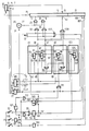
- The drawing which comprises only one Figure, illustrates by means of a block circuit diagram a possible embodiment of a receiver according to the invention.
- In the Figure, a tuning voltage is applied to an input 1 of a
section 3 of the receiver, in response to which thissection 3 is tuned and, upon reception of a transmission an AFC signal is produced at anoutput 5 and a line synchronizing signal at anoutput 7. A line flyback signal is supplied from anoutput 9. It is assumed here that the receiver is a television receiver. In the event of a radio receiver, theoutput 7 can, for example, supply a rectified AFC signal and theoutput 9 an AVC signal. - The
output 5 of thesecion 3 is connected to aninput 11 of atuning signal generator 13, anoutput 15 of which applies to the input of the section 3 a tuning signal which determines the tuning of the receiver. - This tuning signal is, for example, obtained from a digital-to-analog converter arranged at an output of a counter whose counting position can be incremented or decremented, respectively by pulses to be applied to an
input tuning memory 21. As further particulars of this receiver section, which is known per se are not important for an understanding of the invention, they are not shown in the drawing for the sake of clarity. - The pulses at the
inputs tuning signal generator 13 are obtained from AND-gates pulse generator 29, whose frequency is determined by a receiving condition signal applied to aninput 31 thereof. The other input of the AND-gates manual control circuit 37 by means of which a logic one signal can be applied to the relevant input of one of the OR-gates - A further input of the OR-gate 33 and 35, respectively is connected to a forward or
reverse output stop circuit 43, which together with a last-foundtransmission blocking circuit 45 forms part of a search tuning circuit. - This search tuning circuit can be started by applying a forward-start signal to a forward-
start input 47 of the forward-reverse-stop circuit 43. This forward-start signal is received from anoutput 49 of apulse generator 51, which produces a logic one pulse when a logic one signal is produced at itsinput 53 which is connected to an output of an OR-gate 55. This is the case when a searchtuning start switch 57, which is connected to an input of the OR-gate 55, is closed. - The pulse then applied to the forward-
start input 47 of the forward-reverse-stop circuit 43 sets via a clock signal input 59 a first D-flip-flop 61, a D-input 63 of which is connected to a positive voltage. As a result thereof, anoutput 65 of the D-flip-flop 61 becomes one and theoutput 39 of the forward-reverse-stop circuit 43 connected thereto becomes consequently also one, as a result of which the tuning of the receiver is effected in a forward direction. On receipt of a transmission, an AFC signal is produced at theoutput 5 of thesection 3, which signal is applied to aninput 67 of athreshold circuit 69 which in response thereto successively supplies a tuned-too-near or a tuned-too-far signal, respectively from anoutput - The signals at the
outputs section 3 of the receiver are applied torespective inputs coincidence circuit 79 which supplies from itsoutput 81 the receiving state signal which, when there is coincidence between the line synchronizing signals and the line flyback signals is logic one which on reception of a transmission causes the frequency of the signal produced by thepulse generator 29 to be decreased, as a result of which the search rate decreases. - The tuned-too-far signal at the
output 73 of thethreshold circuit 69, which becomes zero when tuning has proceeded too far, is applied to a tuned-too-far input 83 of the forward-reverse-stop circuit 43, which is connected to aclock signal input 85 of a second D-flip-flop 87 a D-input 89 of which is connected to theoutput 65 of the first D-flip-flop 61. Since as described above theoutput 65 of the first D-flip-flop becomes logic one, anoutput 91 of the second D-flip-flop 87 now becomes logic one. The signal at thisoutput 91, which is connected to areset input 95 of the first D-flip-flop 61 via an OR-gate 93, now resets this first D-flip-flop 61. The reverse-stroke output 41 of the forward-reverse-stop circuit 43 connected to theoutput 91 of the second flip-flop 87 is now logic one and the forward-stroke output 39 is logic one; tuning of the receiver now proceeds in the reverse direction. - This reverse movement is stopped by the tuned-too-near signal at the
output 71 of thethreshold circuit 69, which then becomes logic zero and, via aninput 95 of the last found-transmission-blocking circuit 45 and aclock signal input 97 of a third-D-flip-flop 99 sets this third D-flip-flop 99, as its D-input 101 is connected to theoutput 91 of the second D-flip-flop 87, this third D-flip-flop 99 functioning as a first trigger circuit. - An output 103 of the third D-flip-
flop 99 now becomes logic one and via an OR-gate 105 areset input 107 of the second D-flip-flop 87 becomes logic one causing this second D-flip-flop 87 to be reset and the tuning of the receiver to stop. A reset-input 109 of the third D-flip-flop 99 is connected to an output of an OR-gate 111 an input of which receives the receiving state signal from theoutput 81 of thecoincidence circuit 79. As a result thereof the third D-flip-flop 99, which functions as a first trigger circuit, opertes as a last found-transmission-blocking circuit at a restart of the search tuning circuit as it keeps the second D-flip-flop 87 in the reset state until the receiving state signal becomes logic one again, causing the third D-flip-flop 99 to be reset and the reset signal at thereset input 107 of the second D-flip-flop 87 to disappear. - The third D-flip-
flop 99 which functions as a first trigger circuit can also be reset by applying to a second input of the OR-gate 111 a signal which may be received from an AND-gate 113 when acontrol element 115 is operated. In response thereto a divide-by-twodivider 117 changes state and supplies from its output 119 a logic one signal which is applied to agenerator 121 which then supplies a pulse which is applied to an input of the AND-gate 113. the other input of the AND-gate 113 is logic one when the last tuning action of the receiver was manual tuning by means of themanual tuning circuit 37, as will be described in greater detail hereinafter. - So if the last tuning action was a manual tuning action, the third D-flip-flop 99.is reset by the output signal of the OR-gate 111 when the
control element 115 is operated, as a result of which the blocking of the last-found transmission of the search tuning circuit is cancelled. - Restarting the search tuning circuit in response to a starting pulse applied to the forward-start-
input 47 of the forward-reverse-stop circuit 43 renders it possible to tune again to the last-found transmission with the aid of the search tuning circuit. Because of the presence of a tuned-too-far-memory circuit 123 this is even possible when the receiver was detuned too far towards a subsequent transmitter by themanual tuning circuit 37, as a result of which the receiver would move outside the tuning range with a good reception of the last-found transmitter, when the search tuning circuit were started in the forward direction. - The tuned-too-
far memory circuit 123 comprises a fourth D-flip-flop 125 which functions as a second trigger circuit and a clock signal input 127- of which receives the starting signal from theoutput 49 of thepulse generator 51 and a D-input 129 receives the tuned-too-far signal from theoutput 73 of thethreshold circuit 69. Anoutput 131 of the fourth D-flip-flop 125 then becomes logic one, which also holds for a set-input 133 of the second D-flip-flop 876 connected thereto, which creates the reverse stroke state of the forward-reverse-stop circuit 43 and the search tuning circuit yet tunes to the last-found transmission. Areset input 135 of the fourth D-flip-flop 125 is connected to the output of the OR-gate 105 so that also the fourth D-flip-flop 125 is reset, on stopping of the search tuning circuit. - The OR-
gates 93 and 105 have a further input which is connected to an output of an OR-gate 137 the inputs of which are connected to themanual control circuit 37, so that when tuning the receiver is effected manually the search tuning circuit is adjusted to its stop condition. - The output signal of the OR-gate 137 and also the signals at the forward and
reverse outputs output 81 of thecoincidence circuit 79 are applied to an OR-gate 139 whose output is connected to aninput 141 of thetuning signal generator 13, which causes the AFC to be switched off during manual tuning, during search tuning and outside the tuning range in which reception is good. - The output signal of the OR-gate 137 is further applied to a
setting input 143 of a third trigger circuit 145 aresetting input 147 of which is connected to theoutput 49 of thepulse generator 51. So the state of thisthird trigger circuit 145 indicates whether the last tuning operation was a manually effected operation or a search tuning action. In the event it was a manual operation anoutput 149 of thethird trigger circuit 145 becomes logic one and as a consequence thereof also the above-mentioned input of the AND-gate 113 and an input of an AND-gate 151 whose output is connected to a further input of the OR-gate 55, - The further inputs of the AND-gate 151 are connected to the
output 119 of the divide-by-twodivider 117 and to aswitch 153 which is further connected to a write-command signal input 157 of the tuningdata memory circuit 21. A prepare-to-write command input of the tuningdata memory circuit 21 is connected to theoutput 119 of the divide-by-twodivider 117. - When the
control element 115 is operated for the first time, theoutput 119 of the divide-by-twodivider 117 assumes, as stated above, the logic one state as a result of which, as also described above, tuning to the transmission found last is possible when the search tuning action is restarted after manual operation of the transmitter. When thecontrol element 115 is operated for the second time, theoutput 119 of the divide-by-two divider assumes the logic one state, in which situation thepulse generator 121 does not supply a signal and consequently any manual operation of the tuning between the first and the second time thecontrol element 115 is operated, cannot cause a change in the state of the third D-flip-flop. The prepare-to-write command for the tuningdate memory circuit 21 is indeed reinstated thereby, as a result of which a preparation programme which was started the first time thecontrol element 115 was operated is reset to its initial state. - When the
switch 153 is closed, when thecontrol element 115 has been operated for the first time and a manual tuning operation has not been effected, a search tuning action which tunes to the transmission found last as the last-foundtransmission blocking circuit 45 has been adjusted to the reset state because of the fact thecontrol element 115 was operated, is started via the AND-gate 151, the OR-gate 55 and thepulse generator 51. Due to the delay produced by a delay circuit 155 a write command is applied after this search tuning action to theinput 157 of thetuning data memory 21 in which the tuning datum corrected by the search tuning action is then written. Consequently an incorrect value of a tuning datum cannot be written in thetuning date memory 21. - It will be obvious that if so desired the divide-by-two
divider 117 and the input of the AND-gate 151, which input is connected to theswitch 153, can be omitted, as a result of which each time thecontrol element 115 is operated a search tuning action to the transmission found last is started after a manual tuning operation. A still further simplification can be accomplished, if so desired, by also omitting thethird trigger circuit 145 and to substitute a through-connection for the AND-gates pulse generator 121. - To render inoperative the blocking of tuning to the transmission found last at a restart of the search tuning circuit the presence of the tuned-too-
far memory circuit 123 is no absolute condition as will be understood from the above description. - The third and fourth flip-
flops inputs - The expressions set and reset may of course be interchanged when the logic values of the desired input our output signals are chosen differently or if other types of flip-flops are used.
- The forward-reverse-stop circuit may, if so desired, be of a construction different from the construction described in the above embodiment. The same applies for the other portions of the circuit provided they continue to satisfy the conditions mentioned in the Claims.
- The reference numerals included in the Claims are considered to cause no restriction whatsoever of the protective scope thereof.
Claims (4)
Applications Claiming Priority (2)
| Application Number | Priority Date | Filing Date | Title |
|---|---|---|---|
| NL8303203 | 1983-09-16 | ||
| NL8303203A NL8303203A (en) | 1983-09-16 | 1983-09-16 | RECEIVER CONTAINING A TRANSMITTER SWITCH. |
Publications (3)
| Publication Number | Publication Date |
|---|---|
| EP0135970A2 EP0135970A2 (en) | 1985-04-03 |
| EP0135970A3 EP0135970A3 (en) | 1985-06-12 |
| EP0135970B1 true EP0135970B1 (en) | 1988-02-24 |
Family
ID=19842414
Family Applications (1)
| Application Number | Title | Priority Date | Filing Date |
|---|---|---|---|
| EP84201321A Expired EP0135970B1 (en) | 1983-09-16 | 1984-09-12 | Receiver comprising a search tuning circuit |
Country Status (5)
| Country | Link |
|---|---|
| US (1) | US4592094A (en) |
| EP (1) | EP0135970B1 (en) |
| JP (1) | JPS6086907A (en) |
| DE (1) | DE3469474D1 (en) |
| NL (1) | NL8303203A (en) |
Families Citing this family (2)
| Publication number | Priority date | Publication date | Assignee | Title |
|---|---|---|---|---|
| US5134720A (en) * | 1987-09-17 | 1992-07-28 | Amskan Limited | Signal locating apparatus |
| US5739654A (en) * | 1994-12-19 | 1998-04-14 | International Business Machines Corporation | Precision tool control system for a workpiece positioning apparatus |
Family Cites Families (6)
| Publication number | Priority date | Publication date | Assignee | Title |
|---|---|---|---|---|
| JPS601974B2 (en) * | 1978-10-24 | 1985-01-18 | ソニー株式会社 | preset receiver |
| US4387401A (en) * | 1979-05-30 | 1983-06-07 | Rca Corporation | Carrier detector apparatus useful in a multiband sweep type tuning system |
| JPS5750124A (en) * | 1980-09-09 | 1982-03-24 | Mitsubishi Electric Corp | Automatic sweep digital tuning circuit |
| US4419767A (en) * | 1980-11-27 | 1983-12-06 | Pioneer Electronic Corporation | Automatic digital control device for exact frequency tuning of a receiver |
| US4429415A (en) * | 1981-11-30 | 1984-01-31 | Rca Corporation | Signal-seeking tuning system with signal loss protection for a television receiver |
| US4498191A (en) * | 1983-06-06 | 1985-02-05 | General Electric Company | Digital automatic frequency control with tracking |
-
1983
- 1983-09-16 NL NL8303203A patent/NL8303203A/en not_active Application Discontinuation
-
1984
- 1984-09-04 US US06/647,246 patent/US4592094A/en not_active Expired - Fee Related
- 1984-09-12 EP EP84201321A patent/EP0135970B1/en not_active Expired
- 1984-09-12 DE DE8484201321T patent/DE3469474D1/en not_active Expired
- 1984-09-14 JP JP59191848A patent/JPS6086907A/en active Granted
Also Published As
| Publication number | Publication date |
|---|---|
| EP0135970A2 (en) | 1985-04-03 |
| JPS6086907A (en) | 1985-05-16 |
| JPH0451090B2 (en) | 1992-08-18 |
| EP0135970A3 (en) | 1985-06-12 |
| NL8303203A (en) | 1985-04-16 |
| DE3469474D1 (en) | 1988-03-31 |
| US4592094A (en) | 1986-05-27 |
Similar Documents
| Publication | Publication Date | Title |
|---|---|---|
| US4392247A (en) | Broadcast receiver with search tuning | |
| US4121162A (en) | Digital phase locked loop tuning system | |
| US4123724A (en) | Communication equipment | |
| US6529083B2 (en) | Clock control circuit | |
| US4949052A (en) | Clock signal generator having back-up oscillator substitution | |
| US4109283A (en) | Frequency counter for a television tuning system | |
| US4241450A (en) | Automatic turn-off apparatus for a radio or television receiver | |
| US4403344A (en) | Receiver having program reserving function | |
| US4429415A (en) | Signal-seeking tuning system with signal loss protection for a television receiver | |
| US3290611A (en) | Digital frequency control circuit | |
| US4841365A (en) | Arrangement for receiving numerical data, comprising a circuit for recognizing the start of packets | |
| EP0135970B1 (en) | Receiver comprising a search tuning circuit | |
| EP0141445A1 (en) | Stand-alone functional apparatus comprising a micro-computer | |
| EP0125717A1 (en) | Broadcast receiver with automatic broadcast station storage | |
| US4264977A (en) | Search type tuning system | |
| US4337486A (en) | Synchronizing signal discriminator for use in channel selection apparatus of television receiver | |
| US4220973A (en) | Two-speed searching television tuner | |
| US5233425A (en) | Adaptive AFT system with variable step resolution | |
| EP0104688B1 (en) | Receiver comprising a search tuning circuit | |
| US4214274A (en) | Frequency synthesizer tuning system with variable dwell signal seek | |
| US4922344A (en) | Circuit arrangement for evaluating a video synchronizing signal | |
| GB1561340A (en) | Stop-on-signal television broadcast receiver and tuning arrangement therefor | |
| JPS601973B2 (en) | Automatic tuning device for electronic tuner | |
| US5715286A (en) | Digital phase synchronous circuit and data receiving circuit including the same | |
| EP0112599A2 (en) | Pulse corrector |
Legal Events
| Date | Code | Title | Description |
|---|---|---|---|
| PUAI | Public reference made under article 153(3) epc to a published international application that has entered the european phase |
Free format text: ORIGINAL CODE: 0009012 |
|
| AK | Designated contracting states |
Designated state(s): DE FR GB IT |
|
| PUAL | Search report despatched |
Free format text: ORIGINAL CODE: 0009013 |
|
| AK | Designated contracting states |
Designated state(s): DE FR GB IT |
|
| 17P | Request for examination filed |
Effective date: 19851210 |
|
| 17Q | First examination report despatched |
Effective date: 19870518 |
|
| GRAA | (expected) grant |
Free format text: ORIGINAL CODE: 0009210 |
|
| AK | Designated contracting states |
Kind code of ref document: B1 Designated state(s): DE FR GB IT |
|
| ITF | It: translation for a ep patent filed |
Owner name: ING. C. GREGORJ S.P.A. |
|
| REF | Corresponds to: |
Ref document number: 3469474 Country of ref document: DE Date of ref document: 19880331 |
|
| ET | Fr: translation filed | ||
| PLBE | No opposition filed within time limit |
Free format text: ORIGINAL CODE: 0009261 |
|
| STAA | Information on the status of an ep patent application or granted ep patent |
Free format text: STATUS: NO OPPOSITION FILED WITHIN TIME LIMIT |
|
| 26N | No opposition filed | ||
| ITTA | It: last paid annual fee | ||
| ITPR | It: changes in ownership of a european patent |
Owner name: CAMBIO RAGIONE SOCIALE;PHILIPS ELECTRONICS N.V. |
|
| REG | Reference to a national code |
Ref country code: FR Ref legal event code: CD |
|
| PGFP | Annual fee paid to national office [announced via postgrant information from national office to epo] |
Ref country code: DE Payment date: 19951123 Year of fee payment: 12 |
|
| PGFP | Annual fee paid to national office [announced via postgrant information from national office to epo] |
Ref country code: GB Payment date: 19960830 Year of fee payment: 13 |
|
| PGFP | Annual fee paid to national office [announced via postgrant information from national office to epo] |
Ref country code: FR Payment date: 19960925 Year of fee payment: 13 |
|
| PG25 | Lapsed in a contracting state [announced via postgrant information from national office to epo] |
Ref country code: DE Effective date: 19970603 |
|
| PG25 | Lapsed in a contracting state [announced via postgrant information from national office to epo] |
Ref country code: GB Free format text: LAPSE BECAUSE OF NON-PAYMENT OF DUE FEES Effective date: 19970912 |
|
| PG25 | Lapsed in a contracting state [announced via postgrant information from national office to epo] |
Ref country code: FR Free format text: THE PATENT HAS BEEN ANNULLED BY A DECISION OF A NATIONAL AUTHORITY Effective date: 19970930 |
|
| GBPC | Gb: european patent ceased through non-payment of renewal fee |
Effective date: 19970912 |
|
| REG | Reference to a national code |
Ref country code: FR Ref legal event code: ST |