EP0141167A1 - A solid-state image sensor provided with an improved color filter - Google Patents
A solid-state image sensor provided with an improved color filter Download PDFInfo
- Publication number
- EP0141167A1 EP0141167A1 EP84110681A EP84110681A EP0141167A1 EP 0141167 A1 EP0141167 A1 EP 0141167A1 EP 84110681 A EP84110681 A EP 84110681A EP 84110681 A EP84110681 A EP 84110681A EP 0141167 A1 EP0141167 A1 EP 0141167A1
- Authority
- EP
- European Patent Office
- Prior art keywords
- color
- filter
- lights
- rows
- cent
- Prior art date
- Legal status (The legal status is an assumption and is not a legal conclusion. Google has not performed a legal analysis and makes no representation as to the accuracy of the status listed.)
- Granted
Links
Images


Classifications
-
- G—PHYSICS
- G02—OPTICS
- G02B—OPTICAL ELEMENTS, SYSTEMS OR APPARATUS
- G02B5/00—Optical elements other than lenses
- G02B5/20—Filters
- G02B5/201—Filters in the form of arrays
-
- H—ELECTRICITY
- H04—ELECTRIC COMMUNICATION TECHNIQUE
- H04N—PICTORIAL COMMUNICATION, e.g. TELEVISION
- H04N25/00—Circuitry of solid-state image sensors [SSIS]; Control thereof
- H04N25/10—Circuitry of solid-state image sensors [SSIS]; Control thereof for transforming different wavelengths into image signals
- H04N25/11—Arrangement of colour filter arrays [CFA]; Filter mosaics
- H04N25/13—Arrangement of colour filter arrays [CFA]; Filter mosaics characterised by the spectral characteristics of the filter elements
- H04N25/133—Arrangement of colour filter arrays [CFA]; Filter mosaics characterised by the spectral characteristics of the filter elements including elements passing panchromatic light, e.g. filters passing white light
-
- H—ELECTRICITY
- H04—ELECTRIC COMMUNICATION TECHNIQUE
- H04N—PICTORIAL COMMUNICATION, e.g. TELEVISION
- H04N25/00—Circuitry of solid-state image sensors [SSIS]; Control thereof
- H04N25/10—Circuitry of solid-state image sensors [SSIS]; Control thereof for transforming different wavelengths into image signals
- H04N25/11—Arrangement of colour filter arrays [CFA]; Filter mosaics
- H04N25/13—Arrangement of colour filter arrays [CFA]; Filter mosaics characterised by the spectral characteristics of the filter elements
- H04N25/134—Arrangement of colour filter arrays [CFA]; Filter mosaics characterised by the spectral characteristics of the filter elements based on three different wavelength filter elements
Definitions
- This invention relates to a solid-state image sensor such as a charge-coupled imaging device covered with a color filter, and more particularly to an improvement of the color filter.
- An interline type charge-coupled area imaging device is covered with a color filter to obtain a color imaging signal.
- the color filter used for a single-chip CCD imaging device has yellow, cyan and green filters as filter elements which are arranged in rows and columns. By adding and substr.acting between signals produced from adjacent rows, blue and red signals are separated. Green signal is synthesized from the blue and red signals.
- some rows and columns of filter elements lacks filters detecting one of three primary colors.
- a color filter in the prior art first kind of rows is made of yellow filters Ye transmitting red and green lights and green filters G transmitting green light which are placed alternately.
- Second kind of rows is made of cyan filters Cy transmitting blue and green lights and green filters G which are placed alternately.
- the first and second kinds of rows are arranged alternately.
- the first kind of rows cannot detect blue light and the second kind of rows cannot detect red light.
- first kind of columns having yellow filters Ye, cyan filters Cy and green filters G and second kind of columns having green filters G and cyan filters Cy are arranged alternately.
- the second kind of columns cannot detect blue light. Therefore, fine patterns of blue and red cannot be detected, causing a poor resolution in a reproduced picture.
- the object of the present invention is to provide a solid-state color image sensor having a color filter which detects a fine color pattern and causes a high resolution in a reproduced picture.
- a solid-state color image sensor comprising a solid-state imaging device and a color filter formed on the solid-state imaging device and having a matrix of at least three kinds of filter elements arranged in rows and columns, all of the three kinds of filter elements transmitting all the three primary color lights but having transmittances of the three primary color lights such that output signals corresponding to blue and red lights are respectively obtained by subtracting two signals obtained through predetermined two of the three kinds of filter elements from each other.
- the color filter used in the solid-state color image sensor in accordance with the present invention is composed of filter elements each of which transmits all the three primary color lights. Therefore, all the lights can be detected by every filter elements, causing a high resolution in a reproduced picture. Due to the fact that the transmittances of the three primary color lights are set so that output signals corresponding to blue and red lights are respectively obtained by subtracting two signals obtained through predetermined two of the three kinds of filter elements from each other, the output signals corresponding to each of three primary color lights can be respectively derived by using a delay line producing a time delay of one horizontal scanning period, similar to the output from solid-state color imaging device in the prior art. Any special equipment is not required for color imaging apparatus producing a color television signal.
- the interline type charge-coupled imaging device (hereinafter, referred as an IL-CCD image device) is exemplarily shown in Fig. 1.
- a plurality of picture elements 1 which are photo sensors are arranged in rows and columns.
- the photo sensors may be MOS type sensors or diode type sensors.
- vertical CCD shift-registers 2 are provided to shift upward the charges generated at the picture element 1 and transferred to the shift-registers 2.
- a horizontal CCD shift-register 3 is provided to shift charges transferred from the vertical shift-registers 2.
- the charges shifted to the left-hand side of the horizontal CCD shift-register 3 are converted into electrical signals by a charge detector 4.
- the arrows in Fig. 1 show the direction in which charges are transferred.
- signals from the picture elements in one column are followed by signals from the picture elements in the subsequent column.
- a color filter having a plurality of filter elements arranged in a matrix as shown in Fig. 4 which will be explained later covers the IL-CCD imaging device.
- Fig. 2 shows one method for an interlace operation using the IL-CCD imaging device. This method is known as a field accumulation operation.
- the rows of picture elements 1 are numbered as l 1 , l 2 , l 3 , ...l 8 .... in the order from row near the horizontal shift-register 3 to row far from the shift-register 3.
- the charges are transferred to the shift-register 2 from the picture elements 1 in the rows l 2 , l 4 , l 6 , l 8 ... .
- charges are transferred in the shift-registers 2 by a distance corresponding to one interval of rows, charges are transferred to the shift-registers 2 from the picture elements in the rows l 1 , l 3 , l 5 , l 7 ....
- Fig. 3 shows another method for the interlace operation which is called as a frame accumulation operation.
- charges are transferred from the picture elements in rows l 1 , L 3 , l 5 .... to the vertical shift-registers 2 and then to the charge detector 4.
- charges are transferred from the picture elements in the remaining rows l 2 , l 4 , l 6 , l 8.... to the shift-registers 2 and then to the charge detector 4.
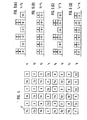
- FIG. 4 A conventional example of the color filter for the frame accumulation operation and adaptable to the IL-CCD imaging device is shown in Fig. 4 which exemplarily demonstrates the arrangement of three types of filter elements 1'.
- the position of each filter element 1' corresponds to the respective picture elements 1 in the IL-CCD imaging device.
- rows of the filter elements 1' are numbered as l 1' l 2' l 3 ... l 8 ...., similary to Figs. 2 and 3.
- yellow filters Ye transmitting red and green lights cyan filters Cy transmitting blue and green lights and green filters G are employed.
- Filter elements are arranged in a period of two elements in column and in a period of four elements in row.
- Figs.5(A) to 5( D ) show values of three primary color signals obtained by the interlacing in accordance with the field accumulation operation.
- B, G and R represent blue, green and red signals, respectively.
- a total value of 1 ⁇ 2 B + 2G + 2R is obtained. This value is used as a luminance signal.
- Blue signal is added to the total value by 1 ⁇ 2 B cos wt where w is a circular frequency corresponding to a period of two filter elements.
- red signal is added by 1 ⁇ 2R cos wt.
- output signals can be expressed as follows:
- Fig. 6 shows a block diagram of conventional color imaging apparatus or a color encoder using a single-chip IL-CCD imaging device.
- the output from the IL-CCD imaging device 6 covered with a color filter 5 is added to a color encoder 8 as a luminance signal through a low-pass filter by which the modulated component of ⁇ 1 ⁇ 2B cos wt + 1 ⁇ 2R cos wt is removed.
- the output from the imaging device 6 is further added to a substracting circuit 10 as a low range luminance signal through another low pass filter 9.
- the output signal is applied to a band-pass filter 11 to separate the modulated component of ⁇ 1 ⁇ 2B cos wt + 2R cos wt.
- the modulated components obtained from lines l 1 and l 2 , l 3 and l 4 , l 2 nad l 3 and l 4 and l 5 are as follows: and
- modulated component is applied to a delay line 12 to cause a time delay of one horizontal scanning period.
- the outputs from the band-pass filter 11 and the delay line 12 are added by an adder 13 to derive a modulated component of red signal, as follows:
- the modulated component of red and blue signals are demodulated by the demodulators 15 and 16, respectively, to obtain red and blue signals.
- the subtracting circuit 10 subtracts the red and blue signal from the low range luminance signal to obtain a green signal. Finally, thus obtained luminance signal, green signal, red signal and blue signal are applied to the color encoder 8 to compose a color television signal.
- the conventional color filter has a drawback as explained later.
- rows l 1 , l 3 , l 5 , l 7 .... since only yellow filters Ye and green filters G are placed, a signal corresponding to blue light cannot be detected.
- blue light can be detected at one filter element (Cy) in every four filter elements.
- the filter elements which detect blue light is one fourth of all the element.
- the filter elements detecting red signal are one in every two element in rows and columns. Therefore, fine patterns of blue and red cannot be detected with high fidelity, resulting in a poor resolution in reproduced picture.
- Fig. 7 is a color filter used in a first embodiment together with an interline type CCD imaging device.
- the CCD imaging device any kind of imaging device may be used.
- An example of the imaging device is as shown in Fig. 1.
- a plurality of filter elements 1 are arranged in rows and columns and composed of yellow filters Ye', green filters G' and cyan filters Cy'.
- the yellow filters Ye' transmit red and green lights and partially transmit blue light.
- the transmittance of blue light is selected to be 20 to 80 per-cent.
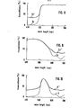
- the transmittance characteristic of the yellow filter Ye l is shown in Fig. 8 in a case where about fourty per-cent of blue light is transmitted.
- the cyan filter Cy' partially transmits red light in addition to blue and green lights.
- the transmittance of red light is selected to be 20 to 80 per-cent.
- Fig. 9 shows its transmittance characteristics in the case where about 40 per-cent of red light is transmitted.
- the green filter G transmits green light and partially transmits blue and red lights.
- the transmittances of blue and red lights are respectively selected to be 20 to 80 per-cent.
- Fig. 10 shows its transmittance characteristics where about 40 per-cent of blue light and about 40 per-cent of red light are transmitted.
- rows one of the yellow and cyan filters and green filters are alternately placed.
- the repetition period of filter elements is two. Ones of columns have a repetition of filters of yellow Ye', cyan Cy', yellow Ye' and green G'. The other columns have a repetition of filters of three greens G' and one cyan Cy'.
- the repetition period of filter elements in columns is four.
- First and third rows l 1 , t 5 .... and l 3 , £ 7 .... have a repetition of a yellow filter Ye' and a green filter G'.
- Second columns l 2 , l 6 .... have a repetition of a cyan filter Cy' and a green filter G'.
- Further filters l 4 , l 8 .... have a repetition of a green filter G' and a cyan filter Cy'.
- the output from the rows l 1 and l 2 and the rows l 2 and l 3 is 1.1B + 2G + 1.1R which is used as a luminance signal.
- the blue and red modulated components are added to the mean output as 0.3B cos wt and 0.3R cos wt where w is a circular frequency corresponding to a period of two filter elements in rows. That is, the output from the rows l 1 and l 2 and the rows l 2 and t 3 may be expressed as follows:
- the added blue modulated component is -0.3 cos wt, while the added red modulated component is 0.3 cos wt. Therefore, the output from the rows l 3 and l 4 and the rows l 4 and l 5 may be expressed as follows:
- the equations (11) and (12) are different in coefficients from the equations (1) to (4) but similar to them. Therefore, the output from the imaging device having a color filter shown in Fig. 7 may be applied to the imaging apparatus having a system block diagram shown in Fig. 6, similar to the prior art, to compose a color television signal.
- the color filter shown in Fig. 7 passes all three primary color lights by more than twenty per-cent, respectively.
- the blue and red lights exposed to any filter elements can be detected and reproduced in a picture.
- the fidelity to the figure to be imaged is improved and a high resolution is achieved in a reproduced picture.
- the transmittances of blue light through the yellow filter Ye', red light through the cyan filter Cy' and blue and red lights through the green filter G' are less than twenty per-cent, the improvements of the fidelity to the figure to be imaged and the resolution in a reproduced picture is not sufficient.
- the transmittances should be selected at least twenty per-cent, and preferably in a range of thirty to sixty per-cent.
- the upper limit of the transmittances is eighty per-cent. If the transmittances are larger than eighty per-cent, amplitudes of modulated signal becomes small, causing an deteriorated signal-to-noise figure.
- the transmittances of the additional light or lights through filter element may be determined independently. By such determination, the rates of blue, red and green lights in the luminance signal may be selected arbitrality. Therefore, a color reproductivity is improved.
- Fig. 12 is another color filter used in a second embodiment of the present invention which covers a CCD imaging device.
- the color filter is composed of white filters W, the yellow filters Ye', the cyan filters Cy' and the green filters G'.
- the transmittances of blue, red and green lights through the yellow, cyan and green filters Ye', Cy' and G' are same as those used in the color filter shown in Fig. 7.
- the white filters W are transparent and transmit all the three primary color lights. Similar to the color filter shown in Fig. 7, the repetitions of filter elements in rows and columns are two and four. Ones of columns have a repetition of filters W, Cy', G' and Cy'. Other columns have a repetition of filters G', Ye', W and Ye'. First rows 5 ....
- Second rows l 2 , l 6 .... have a repetition of filters Cy' and Ye'.
- Third rows l 3 , l 7 .... have a repetition of filters G' and W.
- the fourth rows l 4 , l 8 have a repetition of filters Cy' and Ye'.
- the mean output from the imaging device covered by the color filter shown in Fig. 12 using the filters Ye', Cy' and G' of which transmitting characteristics are shown in Figs. 8 to 10 and the filters W is 1.4R+2G+1.4B which is used as a luminance signal.
- the modulated component of blue signal is 0.6B cos wt in the outputs from the rows l 1 and l 2 and the rows l 4 and l5.
- the modulated component of red signal is -0.6R cos wt in the outputs from the rows l 2 and l 3 and the rows z3 and l 4 .
- the output obtained as the results of the frame accumulation operation may be expressed as follows: and
- the outputs from the rows l 1 and l 2 and the rows l 4 and l 5 have modulated components of blue signal only, while the outputs from the rows l 2 and l 3 and the rows and l 4 have modulated components of red signal only.
- Fig. 13 shows an imaging apparatus used for composing a color television signal from a single-chip CCD imaging device 6 covered by a color filter 5 shown in Fig. 12.
- the same reference numerals representing the same components as in Fig. 6 are employed.
- the output from the imaging device 6 is applied to the color encoder 8 as a luminance signal through a low-pass filter 7.
- the output is also applied to the color encoder 8 as a low range luminance signal through another low-pass filter 9 which passes lower frequency component than the low pass filter 7.
- the output is further applied to a band-pass filter 11 having a center frequency of the circular frequency w.
- the modulated components of blue and red signals are separated from the output from the imaging device 6 by the band-pass filter 11.
- the separated components are demodulated in the demodulator 15.
- blue signal is obtained from the output from the rows l 1 and l 2 and the rows l 4 and l 5
- red signal is obtained from the output from the rows l 3 and l 4 and the rows l 4 + l 5 .
- the demodulated signal is applied to the delay line 12 having a time delay of one horizontal scanning period. In horizontal scanning periods corresponding to outputs from the rows l 1 and L 2 and the rows L4 and l 5 , the delayed signal and non-delayed signal are applied to the color encoder 8 as blue and red signals, respectively.
- the non-delayed and delayed signals are applied to the color encoder 8 as blue and red signals, respectively.
- This switch is made by the switch 17.
- the color encoder 8 composes a color television signal.
- the improvements in a high fidelity and a high resolution are achieved in cases using the color filter shown in Fig. 12, similarly to the case using the color filter shown in Fig. 7.
- the imaging device covered with the color filter shown in Fig. 12 requires neither adder nor subtractor to synthesize blue and red signal from the output therefrom. That is, the imaging apparatus can be made simple by using the color filter shown in Fig. 12.
- Fig. 14 shows still other color filter used in a third embodiment of the present invention.
- the color filter is made of, as filter elements, filters Ye', Cy' and G' of which transmitting characteristics are the same as those in Fig. 12 and magenta filters Mg.
- the magenta filters Mg transmit blue and red lights and about fifty per-cent of green light as shown in Fig. 15.
- the color filter uses the magenta filters Mg in place of the white filters W used in the color filter shown in Fig. 12.
- the arrangement of other filters Te', Cy' and G' is similar to the color filter shown in Fig. 12.
- the mean output of imaging device covered with the color filter shown in Fi g . 14 is 1.4B +1.75G +1.4G which is used as a luminance signal.
- a color difference signal of (0.6B - 0.25G) is modulated with a circular frequency w and added to the luminance signal, as follows:
- a color difference signal of -(0.6R - 0.25G) is modulated with the circular frequency w and added to the luminance signal, as follows:
- a color television signal may be composed of the imaging apparatus as shown in Fig. 13.
- the imaging device covered with the color filter shown in Fig. 14 has advantages similar to the imaging device covered with the color filter shown in Fig. 12. The fidelity and resolution in a reproduced picture are further improved.
- the imaging apparatus for composing a color television signal from the output of the imaging device is made simple.
- an interline type CCD imaging device is used as an imaging device to be covered with color filters shown in Figs. 7, 12 and 14.
- the imaging device is not limited to the interline type CCD imaging device.
- a frame transfer type CCD imaging device may be used.
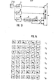
- the frame transfer type CCD imaging device covered with a color filter shown in Fig. 7 is examplarily shown in Fig. 16.
- a plurality of transparent electrodes 21 are isolatedly disposed on a silicon substrate 20.
- a color filter 22 covers the electrodes 21 so that one filter element covers two electrodes. For transferring charges, four phase pulses ⁇ 1 , ⁇ 2 , ⁇ 3 and ⁇ 4 are used.
- the pulses ⁇ 1 and ⁇ 2 are applied to the electrodes 21 under the filter element in rows l 2 , l 4 , 46 .... .
- the remaining clock pulses ⁇ 3 and ⁇ 4 are applied to other electrodes 21 under the filter elements in rows l 1 , l 3 , l 5 .
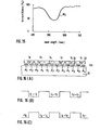
- Figs. 16(B) and 16(C) show potential distributions under electrodes.
- the clocks ⁇ 2 and ⁇ 3 take a potential which generates potential wells in the substrate 20 in odd number fields, as shown in Fig. 16(B), mixing outputs based on two filter elements in the rows l 1 and l 2 , the rows l 3 and l 4 , the rows l 5 and l 6 and so on.
- the clocks ⁇ 1 , ⁇ 2 , ⁇ 3 and ⁇ 4 changes transfer pulses having four phases to transfer the accumulated charges in the direction along the arrow.
- the clocks ⁇ 1 and ⁇ 4 take a potential which generates potential wells in the substrate, as shown in Fig. 16(C), mixing outputs based on two filter elements in the rows l 2 and l 3 the rows t4 and l 5 and so on.
- the clocks ⁇ 1 , ⁇ 2 , ⁇ 3 and ⁇ 4 return to the original transfer pulses having four phases to transfer the accumulated charges in the direction along the arrow.
- the color television signal may be composed by the imaging apparatus as shown in Fig. 6 or 13.
Landscapes
- Physics & Mathematics (AREA)
- Spectroscopy & Molecular Physics (AREA)
- Engineering & Computer Science (AREA)
- Multimedia (AREA)
- Signal Processing (AREA)
- General Physics & Mathematics (AREA)
- Optics & Photonics (AREA)
- Color Television Image Signal Generators (AREA)
- Optical Filters (AREA)
- Solid State Image Pick-Up Elements (AREA)
Abstract
Description
- This invention relates to a solid-state image sensor such as a charge-coupled imaging device covered with a color filter, and more particularly to an improvement of the color filter.
- An interline type charge-coupled area imaging device is covered with a color filter to obtain a color imaging signal. The color filter used for a single-chip CCD imaging device has yellow, cyan and green filters as filter elements which are arranged in rows and columns. By adding and substr.acting between signals produced from adjacent rows, blue and red signals are separated. Green signal is synthesized from the blue and red signals.
- However, according to the arrangement of the filter elements in the prior art, some rows and columns of filter elements lacks filters detecting one of three primary colors. For example, a color filter in the prior art, first kind of rows is made of yellow filters Ye transmitting red and green lights and green filters G transmitting green light which are placed alternately. Second kind of rows is made of cyan filters Cy transmitting blue and green lights and green filters G which are placed alternately. The first and second kinds of rows are arranged alternately. The first kind of rows cannot detect blue light and the second kind of rows cannot detect red light. Similarly, first kind of columns having yellow filters Ye, cyan filters Cy and green filters G and second kind of columns having green filters G and cyan filters Cy are arranged alternately. The second kind of columns cannot detect blue light. Therefore, fine patterns of blue and red cannot be detected, causing a poor resolution in a reproduced picture.
- The object of the present invention is to provide a solid-state color image sensor having a color filter which detects a fine color pattern and causes a high resolution in a reproduced picture.
- According to the present invention, there is provided a solid-state color image sensor comprising a solid-state imaging device and a color filter formed on the solid-state imaging device and having a matrix of at least three kinds of filter elements arranged in rows and columns, all of the three kinds of filter elements transmitting all the three primary color lights but having transmittances of the three primary color lights such that output signals corresponding to blue and red lights are respectively obtained by subtracting two signals obtained through predetermined two of the three kinds of filter elements from each other.
- The color filter used in the solid-state color image sensor in accordance with the present invention is composed of filter elements each of which transmits all the three primary color lights. Therefore, all the lights can be detected by every filter elements, causing a high resolution in a reproduced picture. Due to the fact that the transmittances of the three primary color lights are set so that output signals corresponding to blue and red lights are respectively obtained by subtracting two signals obtained through predetermined two of the three kinds of filter elements from each other, the output signals corresponding to each of three primary color lights can be respectively derived by using a delay line producing a time delay of one horizontal scanning period, similar to the output from solid-state color imaging device in the prior art. Any special equipment is not required for color imaging apparatus producing a color television signal.
- The above and further objects, features and advantages of the present invention will become more apparent from the following detailed description taken in conjunction with the accompanying drawings, wherein:
- Fig. 1 is a schematical plan view of an interline- type CCD imaging device in the prior art;
- Fig. 2 is an explanatory view showing a process for leading out charges accumulated in the CCD imaging device in accordance with a field accumulation operation;
- Fig. 3 is an explanatory view showing a process for leading out charges accumulated in the CCD imaging device in accordance with a frame accumulation operation;
- Fig. 4 is a plan view of the color filter in the prior art showing an arrangement of filter elements;
- Figs.5(A) to 5(D) are explanatory views showing outputs obtained from the imaging device having the color filter shown in Fig. 4;
- Fig. 6 is a block diagram showing an imaging apparatus using a single-chip interline type CCD imaging device;
- Fig. 7 is a plan view of the color filter used in a first embodiment of the present invention;
- Figs. 8, 9 and 10 are graphs showing transmittances of yellow, cyan and green filters;
- Figs. 11(A) to 11(D) are explanatory views showing outputs obtained from the imaging device having the color filter shown in Fig. 7;
- Fig. 12 is a plan view of the color filter used in a second embodiment of the present invention;
- Fig. 13 is a block diagram showing a color imaging apparatus in which the color filters improved by the present invention are adaptable;
- Fig. 14 is a plan view of the color filter used in a third embodiment of the present invention;
- Fig. 15 is a graph showing a transmittance of magenda filter; and
- Figs.16(A) to 16(C) show a sectional view of frame transfer type CCD imaging device and diagrams showing its potential distributions.
- The interline type charge-coupled imaging device (hereinafter, referred as an IL-CCD image device) is exemplarily shown in Fig. 1. A plurality of
picture elements 1 which are photo sensors are arranged in rows and columns. The photo sensors may be MOS type sensors or diode type sensors. Along the rows, vertical CCD shift-registers 2 are provided to shift upward the charges generated at thepicture element 1 and transferred to the shift-registers 2. At one ends of the shift-registers 2, a horizontal CCD shift-register 3 is provided to shift charges transferred from the vertical shift-registers 2. The charges shifted to the left-hand side of the horizontal CCD shift-register 3 are converted into electrical signals by a charge detector 4. The arrows in Fig. 1 show the direction in which charges are transferred. In the output signal, signals from the picture elements in one column are followed by signals from the picture elements in the subsequent column. For color image sensing, a color filter having a plurality of filter elements arranged in a matrix as shown in Fig. 4 which will be explained later covers the IL-CCD imaging device. - Fig. 2 shows one method for an interlace operation using the IL-CCD imaging device. This method is known as a field accumulation operation. Here, the rows of
picture elements 1 are numbered as ℓ1, ℓ2, ℓ3, ...ℓ8 .... in the order from row near the horizontal shift-register 3 to row far from the shift-register 3. In odd number fields, the charges are transferred to the shift-register 2 from thepicture elements 1 in the rows ℓ2, ℓ4, ℓ6, ℓ8... . After charges are transferred in the shift-registers 2 by a distance corresponding to one interval of rows, charges are transferred to the shift-registers 2 from the picture elements in the rows ℓ1, ℓ3, ℓ5, ℓ7 .... to add charges from rows ℓ1 and ℓ2, ℓ3 and 24, ℓ5 and ℓ6 ℓ7 and ℓ8 ... in the vertical shift-registers 2. Thereafter, the added charges are transferred to the horizontal shift-register 3 and then to the charge detector 4. In the even number fields, the charges accumulated in the picture elements in rows ℓ1,ℓ3, ℓ5, ℓ7 .... are transferred to the vertical shift-registers 2, and then charges accumulated in the picture elements in rows ℓ2, ℓ4, ℓ6, ℓ8 .... are transferred to the shift-registers 2 after the shift-registers 2 shift charges by a distance corresponding to an interval between rows. As a results, charges from rows ℓ2 and ℓ3, ℓ4 and ℓ5, ℓ6 and L7 .... are respectively added and transferred to the charge detector 4. - Fig. 3 shows another method for the interlace operation which is called as a frame accumulation operation. In the odd number fields, charges are transferred from the picture elements in rows ℓ1, L3, ℓ5 .... to the vertical shift-
registers 2 and then to the charge detector 4. In the even number fields, charges are transferred from the picture elements in the remaining rows ℓ2, ℓ4, ℓ6, ℓ8.... to the shift-registers 2 and then to the charge detector 4. - The interlace operation according to the frame accumulation operation is now mainly used. Therefore, the following explanation will be made with reference to the frame accumulation operation.
- A conventional example of the color filter for the frame accumulation operation and adaptable to the IL-CCD imaging device is shown in Fig. 4 which exemplarily demonstrates the arrangement of three types of filter elements 1'. The position of each filter element 1' corresponds to the
respective picture elements 1 in the IL-CCD imaging device. Then,rows of the filter elements 1' are numbered as ℓ1' ℓ2' ℓ3 ... ℓ8 ...., similary to Figs. 2 and 3. As the filter elements 1', yellow filters Ye transmitting red and green lights cyan filters Cy transmitting blue and green lights and green filters G are employed. Filter elements are arranged in a period of two elements in column and in a period of four elements in row. That is, in rows ℓ1' ℓ5 ...., yellow and green filters Ye and G are placed in this order. In subsequent rows ℓ2, ℓ6, ..., cyan and green filters Cy and G are placed in this order. In rows ℓ3, ℓ7, ...., yellow any green filters Ye and G are placed in this order. In the remaining rows ℓ4, ℓ8, ..., green and cyan filters G and Cy are placed in this order. - Figs.5(A) to 5(D) show values of three primary color signals obtained by the interlacing in accordance with the field accumulation operation. In the drawing, B, G and R represent blue, green and red signals, respectively. By adding all the color signals in the subsequent two rows, a total value of ½ B + 2G + 2R is obtained. This value is used as a luminance signal. Blue signal is added to the total value by ½ B cos wt where w is a circular frequency corresponding to a period of two filter elements. Similarly, red signal is added by ½R cos wt. In the output from rows ℓ3 and ℓ4 and ℓ4 and ℓ5, the phase of blue signal is opposite to other outputs from rows ℓ1 and ℓ2 and ℓ2 and ℓ3. As a result, output signals can be expressed as follows:


- Fig. 6 shows a block diagram of conventional color imaging apparatus or a color encoder using a single-chip IL-CCD imaging device. The output from the IL-
CCD imaging device 6 covered with acolor filter 5 is added to acolor encoder 8 as a luminance signal through a low-pass filter by which the modulated component of ±½B cos wt + ½R cos wt is removed. The output from theimaging device 6 is further added to asubstracting circuit 10 as a low range luminance signal through anotherlow pass filter 9. In addition, the output signal is applied to a band-pass filter 11 to separate the modulated component of ±½B cos wt + 2R cos wt. The modulated components obtained from lines ℓ1 and ℓ2, ℓ3 and ℓ4, ℓ2 nad ℓ3 and ℓ4 and ℓ5 are as follows:


- Thus obtained modulated component is applied to a
delay line 12 to cause a time delay of one horizontal scanning period. The outputs from the band-pass filter 11 and thedelay line 12 are added by anadder 13 to derive a modulated component of red signal, as follows:

- On the other hand, the outputs from the band-
pass filter 11 and thedelay line 12 are subtracted from each other to derive a modulated component of blue signal, as follows:

- The modulated component of red and blue signals are demodulated by the
demodulators circuit 10 subtracts the red and blue signal from the low range luminance signal to obtain a green signal. Finally, thus obtained luminance signal, green signal, red signal and blue signal are applied to thecolor encoder 8 to compose a color television signal. - Returning to Fig. 4, the conventional color filter has a drawback as explained later. In rows ℓ1, ℓ3, ℓ5, ℓ7 ...., since only yellow filters Ye and green filters G are placed, a signal corresponding to blue light cannot be detected. In columns, blue light can be detected at one filter element (Cy) in every four filter elements. As a whole, the filter elements which detect blue light is one fourth of all the element. Similarly, the filter elements detecting red signal are one in every two element in rows and columns. Therefore, fine patterns of blue and red cannot be detected with high fidelity, resulting in a poor resolution in reproduced picture.
- Fig. 7 is a color filter used in a first embodiment together with an interline type CCD imaging device. As the CCD imaging device, any kind of imaging device may be used. An example of the imaging device is as shown in Fig. 1. A plurality of
filter elements 1 are arranged in rows and columns and composed of yellow filters Ye', green filters G' and cyan filters Cy'. The yellow filters Ye' transmit red and green lights and partially transmit blue light. The transmittance of blue light is selected to be 20 to 80 per-cent. The transmittance characteristic of the yellow filter Yel is shown in Fig. 8 in a case where about fourty per-cent of blue light is transmitted. The cyan filter Cy' partially transmits red light in addition to blue and green lights. The transmittance of red light is selected to be 20 to 80 per-cent. Fig. 9 shows its transmittance characteristics in the case where about 40 per-cent of red light is transmitted. The green filter G transmits green light and partially transmits blue and red lights. The transmittances of blue and red lights are respectively selected to be 20 to 80 per-cent. Fig. 10 shows its transmittance characteristics where about 40 per-cent of blue light and about 40 per-cent of red light are transmitted. In rows, one of the yellow and cyan filters and green filters are alternately placed. The repetition period of filter elements is two. Ones of columns have a repetition of filters of yellow Ye', cyan Cy', yellow Ye' and green G'. The other columns have a repetition of filters of three greens G' and one cyan Cy'. The repetition period of filter elements in columns is four. First and third rows ℓ1, t5 .... and ℓ3, £7 .... have a repetition of a yellow filter Ye' and a green filter G'. Second columns ℓ2, ℓ6 .... have a repetition of a cyan filter Cy' and a green filter G'. Further filters ℓ4, ℓ8 .... have a repetition of a green filter G' and a cyan filter Cy'. By adding the charge signals obtained from subsequent two rows in accordance with the frame accumulation operation, there are obtained output signals as shown in Fig. 11 in which B, G and R represent blue, green and red signals, respectively. A mean output of three primary signal when the filters having the characteristics shown in Figs. 8, 9 and 10 are used is 1.1B + 2G + 1.1R which is used as a luminance signal. In the outputs from the rows ℓ1 and ℓ2 and the rows ℓ2 and ℓ3, the blue and red modulated components are added to the mean output as 0.3B cos wt and 0.3R cos wt where w is a circular frequency corresponding to a period of two filter elements in rows. That is, the output from the rows ℓ1 and ℓ2 and the rows ℓ2 and t3 may be expressed as follows: -


- The equations (11) and (12) are different in coefficients from the equations (1) to (4) but similar to them. Therefore, the output from the imaging device having a color filter shown in Fig. 7 may be applied to the imaging apparatus having a system block diagram shown in Fig. 6, similar to the prior art, to compose a color television signal.
- The color filter shown in Fig. 7 passes all three primary color lights by more than twenty per-cent, respectively. The blue and red lights exposed to any filter elements can be detected and reproduced in a picture. The fidelity to the figure to be imaged is improved and a high resolution is achieved in a reproduced picture. Here, if the transmittances of blue light through the yellow filter Ye', red light through the cyan filter Cy' and blue and red lights through the green filter G' are less than twenty per-cent, the improvements of the fidelity to the figure to be imaged and the resolution in a reproduced picture is not sufficient. To the sufficient improvements, the transmittances should be selected at least twenty per-cent, and preferably in a range of thirty to sixty per-cent. The upper limit of the transmittances is eighty per-cent. If the transmittances are larger than eighty per-cent, amplitudes of modulated signal becomes small, causing an deteriorated signal-to-noise figure.
- Further, the transmittances of the additional light or lights through filter element may be determined independently. By such determination, the rates of blue, red and green lights in the luminance signal may be selected arbitrality. Therefore, a color reproductivity is improved.
- Fig. 12 is another color filter used in a second embodiment of the present invention which covers a CCD imaging device. The color filter is composed of white filters W, the yellow filters Ye', the cyan filters Cy' and the green filters G'. The transmittances of blue, red and green lights through the yellow, cyan and green filters Ye', Cy' and G' are same as those used in the color filter shown in Fig. 7. The white filters W are transparent and transmit all the three primary color lights. Similar to the color filter shown in Fig. 7, the repetitions of filter elements in rows and columns are two and four. Ones of columns have a repetition of filters W, Cy', G' and Cy'. Other columns have a repetition of filters G', Ye', W and Ye'.
First rows 5 .... have a repetition of filters W and G'. Second rows ℓ2, ℓ6 .... have a repetition of filters Cy' and Ye'. Third rows ℓ3, ℓ7 .... have a repetition of filters G' and W. The fourth rows ℓ4, ℓ8 have a repetition of filters Cy' and Ye'. - The mean output from the imaging device covered by the color filter shown in Fig. 12 using the filters Ye', Cy' and G' of which transmitting characteristics are shown in Figs. 8 to 10 and the filters W is 1.4R+2G+1.4B which is used as a luminance signal. The modulated component of blue signal is 0.6B cos wt in the outputs from the rows ℓ1 and ℓ2 and the rows ℓ4 and ℓ5. The modulated component of red signal is -0.6R cos wt in the outputs from the rows ℓ2 and ℓ3 and the rows z3 and ℓ4. Therefore, the output obtained as the results of the frame accumulation operation may be expressed as follows:


- Fig. 13 shows an imaging apparatus used for composing a color television signal from a single-chip
CCD imaging device 6 covered by acolor filter 5 shown in Fig. 12. The same reference numerals representing the same components as in Fig. 6 are employed. The output from theimaging device 6 is applied to thecolor encoder 8 as a luminance signal through a low-pass filter 7. The output is also applied to thecolor encoder 8 as a low range luminance signal through another low-pass filter 9 which passes lower frequency component than thelow pass filter 7. The output is further applied to a band-pass filter 11 having a center frequency of the circular frequency w. The modulated components of blue and red signals are separated from the output from theimaging device 6 by the band-pass filter 11. The separated components are demodulated in thedemodulator 15. As a result, blue signal is obtained from the output from the rows ℓ1 and ℓ2 and the rows ℓ4 and ℓ5, while red signal is obtained from the output from the rows ℓ3 and ℓ4 and the rows ℓ4 + ℓ5. The demodulated signal is applied to thedelay line 12 having a time delay of one horizontal scanning period. In horizontal scanning periods corresponding to outputs from the rows ℓ1 and L2 and the rows L4 and ℓ5, the delayed signal and non-delayed signal are applied to thecolor encoder 8 as blue and red signals, respectively. In the other horizontal scanning periods corresponding to outputs from the rows ℓ3 and ℓ4 and the rows ℓ4 and ℓ5, the non-delayed and delayed signals are applied to thecolor encoder 8 as blue and red signals, respectively. This switch is made by theswitch 17. Thecolor encoder 8 composes a color television signal. - The improvements in a high fidelity and a high resolution are achieved in cases using the color filter shown in Fig. 12, similarly to the case using the color filter shown in Fig. 7. The imaging device covered with the color filter shown in Fig. 12 requires neither adder nor subtractor to synthesize blue and red signal from the output therefrom. That is, the imaging apparatus can be made simple by using the color filter shown in Fig. 12.
- Fig. 14 shows still other color filter used in a third embodiment of the present invention. The color filter is made of, as filter elements, filters Ye', Cy' and G' of which transmitting characteristics are the same as those in Fig. 12 and magenta filters Mg. The magenta filters Mg transmit blue and red lights and about fifty per-cent of green light as shown in Fig. 15. The color filter uses the magenta filters Mg in place of the white filters W used in the color filter shown in Fig. 12. The arrangement of other filters Te', Cy' and G' is similar to the color filter shown in Fig. 12.
- When the respective color filters Ye', Cy', G' and Mg have the transmitting characteristics of Figs. 8, 9, 10 and 15, the mean output of imaging device covered with the color filter shown in Fig. 14 is 1.4B +1.75G +1.4G which is used as a luminance signal. In outputs from the rows ℓ1 and ℓ2 and the rows ℓ4 and ℓ5, a color difference signal of (0.6B - 0.25G) is modulated with a circular frequency w and added to the luminance signal, as follows:


- The outputs from the rows ℓ1 and ℓ2 and the rows ℓ4 and ℓ5 have a modulated component of (0.65-0.25G) cos wt only, while the outputs from the rows z2 and ℓ3 and the rows ℓ3 and ℓ4 have a modulated component of-(0.6R-0.25G) cos wt only. Therefore, a color television signal may be composed of the imaging apparatus as shown in Fig. 13.
- The imaging device covered with the color filter shown in Fig. 14 has advantages similar to the imaging device covered with the color filter shown in Fig. 12. The fidelity and resolution in a reproduced picture are further improved. The imaging apparatus for composing a color television signal from the output of the imaging device is made simple.
- In the above, an interline type CCD imaging device is used as an imaging device to be covered with color filters shown in Figs. 7, 12 and 14. The imaging device is not limited to the interline type CCD imaging device. A frame transfer type CCD imaging device may be used. The frame transfer type CCD imaging device covered with a color filter shown in Fig. 7 is examplarily shown in Fig. 16. A plurality of
transparent electrodes 21 are isolatedly disposed on asilicon substrate 20. Acolor filter 22 covers theelectrodes 21 so that one filter element covers two electrodes. For transferring charges, four phase pulses ∅1, ∅2, ∅3 and ∅4 are used. The pulses ∅1 and ∅2 are applied to theelectrodes 21 under the filter element in rows ℓ2, ℓ4, 46 .... . The remaining clock pulses ∅3 and ∅4 are applied toother electrodes 21 under the filter elements in rows ℓ1, ℓ3, ℓ5..... - Figs. 16(B) and 16(C) show potential distributions under electrodes. For interlacing, the clocks ∅2 and ∅3 take a potential which generates potential wells in the
substrate 20 in odd number fields, as shown in Fig. 16(B), mixing outputs based on two filter elements in the rows ℓ1 and ℓ2, the rows ℓ3 and ℓ4, the rows ℓ5 and ℓ6 and so on. After the charge accumulation, the clocks ∅1, ∅2, ∅3 and ∅4 changes transfer pulses having four phases to transfer the accumulated charges in the direction along the arrow. On the other hand, in even number fields, the clocks ∅1 and ∅4 take a potential which generates potential wells in the substrate, as shown in Fig. 16(C), mixing outputs based on two filter elements in the rows ℓ2 and ℓ3 the rows t4 and ℓ5 and so on. After the charge accumulation, the clocks ∅1, ∅2, ∅3 and ∅4 return to the original transfer pulses having four phases to transfer the accumulated charges in the direction along the arrow. - The accumulated charges for the odd and even number fields have similar combination of rows in color filter to the charges mixed in accordance with the use of the interline type CCD imaging device. Therefore, the color television signal may be composed by the imaging apparatus as shown in Fig. 6 or 13.
- Although some embodiments are erplained in the above, it is apparent to the skilled in the art that the kinds of filter element adaptable to the color filter, the transmitting characteristics of filter elements and/or the arrangement of filter elements are not limited to the embodiments.
Claims (6)
Applications Claiming Priority (2)
| Application Number | Priority Date | Filing Date | Title |
|---|---|---|---|
| JP164493/83 | 1983-09-07 | ||
| JP58164493A JPS6055781A (en) | 1983-09-07 | 1983-09-07 | Solid-state image pickup element |
Publications (2)
| Publication Number | Publication Date |
|---|---|
| EP0141167A1 true EP0141167A1 (en) | 1985-05-15 |
| EP0141167B1 EP0141167B1 (en) | 1988-12-14 |
Family
ID=15794202
Family Applications (1)
| Application Number | Title | Priority Date | Filing Date |
|---|---|---|---|
| EP84110681A Expired EP0141167B1 (en) | 1983-09-07 | 1984-09-07 | A solid-state image sensor provided with an improved color filter |
Country Status (4)
| Country | Link |
|---|---|
| US (1) | US4652911A (en) |
| EP (1) | EP0141167B1 (en) |
| JP (1) | JPS6055781A (en) |
| DE (1) | DE3475687D1 (en) |
Cited By (4)
| Publication number | Priority date | Publication date | Assignee | Title |
|---|---|---|---|---|
| EP0164255A2 (en) * | 1984-05-31 | 1985-12-11 | Nec Corporation | Solid-state color imaging apparatus |
| EP0247562A1 (en) * | 1986-05-26 | 1987-12-02 | Sony Corporation | Color filter arrangement for CCD imager |
| EP0403850A2 (en) * | 1989-06-19 | 1990-12-27 | Polaroid Corporation | Color encoding photographic film |
| EP0485221A2 (en) * | 1990-11-08 | 1992-05-13 | Sony Corporation | A solid-state image pick-up device having a color filter |
Families Citing this family (16)
| Publication number | Priority date | Publication date | Assignee | Title |
|---|---|---|---|---|
| JPS60103790A (en) * | 1983-11-10 | 1985-06-08 | Nec Corp | Color solid-state image pickup device |
| US4907074A (en) * | 1985-10-31 | 1990-03-06 | Canon Kabushiki Kaisha | Image pickup apparatus having color separation filters and forming line-sequential luminance and color-difference signals |
| JP2677550B2 (en) * | 1986-02-18 | 1997-11-17 | 株式会社東芝 | Solid-state imaging device |
| US4916528A (en) * | 1987-12-28 | 1990-04-10 | Victor Company Of Japan, Ltd. | Color stripe filter in color image pickup apparatus |
| FR2722901A1 (en) * | 1994-07-21 | 1996-01-26 | C2L Gestion | Standardised postcode indication system for postal envelope |
| US6292212B1 (en) * | 1994-12-23 | 2001-09-18 | Eastman Kodak Company | Electronic color infrared camera |
| DE69712969T2 (en) * | 1996-03-29 | 2003-01-09 | Sanyo Electric Co | Color camera with a single, higher resolution CCD color sensor capable of limiting ghost color generation |
| US6035077A (en) * | 1996-05-03 | 2000-03-07 | Omnivision Technologies, Inc. | Single-chip color CMOS image sensor with two or more line reading structure and high-sensitivity interlace color structure |
| US5901257A (en) * | 1996-05-03 | 1999-05-04 | Omnivision Technologies, Inc. | Single chip color MOS image sensor with two line reading structure and improved color filter pattern |
| US6289139B1 (en) | 1996-05-03 | 2001-09-11 | Omnivision Technologies, Inc. | Single chip color CMOS image sensor with two or more line reading structure |
| US6665009B1 (en) * | 1998-05-20 | 2003-12-16 | Omnivision Technologies, Inc. | On-chip dead pixel correction in a CMOS imaging sensor |
| US6914627B1 (en) | 1998-05-27 | 2005-07-05 | Omnivision Technologies, Inc. | Method and apparatus for digital column fixed pattern noise canceling for a CMOS image sensor |
| US6707496B1 (en) | 1999-09-15 | 2004-03-16 | Omnivision Technologies, Inc. | CMOS sensor having analog delay line for image processing |
| KR101324198B1 (en) * | 2007-10-05 | 2013-11-06 | 삼성전자주식회사 | Improved solid state image sensing device, Method for arranging pixels and processing signals for the same |
| US9749607B2 (en) | 2009-07-16 | 2017-08-29 | Digimarc Corporation | Coordinated illumination and image signal capture for enhanced signal detection |
| US9727941B1 (en) * | 2014-11-19 | 2017-08-08 | Digimarc Corporation | Optimizing optical scanners for digital watermark detection |
Citations (1)
| Publication number | Priority date | Publication date | Assignee | Title |
|---|---|---|---|---|
| DE2904813A1 (en) * | 1978-02-10 | 1979-08-16 | Hitachi Ltd | MONOLITHIC COLOR IMAGE RECORDING DEVICE |
Family Cites Families (6)
| Publication number | Priority date | Publication date | Assignee | Title |
|---|---|---|---|---|
| JPS6019718B2 (en) * | 1976-10-20 | 1985-05-17 | 松下電器産業株式会社 | Color solid-state imaging device |
| US4437112A (en) * | 1980-02-15 | 1984-03-13 | Canon Kabushiki Kaisha | Solid-state color imaging apparatus |
| JPS574680A (en) * | 1980-06-11 | 1982-01-11 | Matsushita Electric Ind Co Ltd | Color solid-state pickup device |
| JPS57109488A (en) * | 1980-12-26 | 1982-07-07 | Matsushita Electric Ind Co Ltd | Solid color image pickup device |
| JPS57203387A (en) * | 1981-06-10 | 1982-12-13 | Toshiba Corp | Color television image pickup device |
| JPS58211718A (en) * | 1982-06-04 | 1983-12-09 | Hitachi Denshi Ltd | Image pickup device |
-
1983
- 1983-09-07 JP JP58164493A patent/JPS6055781A/en active Granted
-
1984
- 1984-09-06 US US06/647,742 patent/US4652911A/en not_active Expired - Lifetime
- 1984-09-07 DE DE8484110681T patent/DE3475687D1/en not_active Expired
- 1984-09-07 EP EP84110681A patent/EP0141167B1/en not_active Expired
Patent Citations (1)
| Publication number | Priority date | Publication date | Assignee | Title |
|---|---|---|---|---|
| DE2904813A1 (en) * | 1978-02-10 | 1979-08-16 | Hitachi Ltd | MONOLITHIC COLOR IMAGE RECORDING DEVICE |
Non-Patent Citations (2)
| Title |
|---|
| PATENT ABSTRACTS OF JAPAN, unexamined applications, E field, vol. 6, no. 200, October 9, 1982 THE PATENT OFFICE JAPANESE GOVERNMENT page 123 E 135 & JP-A-57-109 488 (A) (matsushita) * |
| PATENT ABSTRACTS OF JAPAN, unexamined applications, E field, vol. 7, no. 58, March 10, 1983 THE PATENT OFFICE JAPANESE GOVERNMENT page 6 E 163 & JP-A-57-203 387 (A) (tokyo shibaura denki) * |
Cited By (7)
| Publication number | Priority date | Publication date | Assignee | Title |
|---|---|---|---|---|
| EP0164255A2 (en) * | 1984-05-31 | 1985-12-11 | Nec Corporation | Solid-state color imaging apparatus |
| EP0164255A3 (en) * | 1984-05-31 | 1989-04-26 | Nec Corporation | Solid-state color imaging apparatus |
| EP0247562A1 (en) * | 1986-05-26 | 1987-12-02 | Sony Corporation | Color filter arrangement for CCD imager |
| EP0403850A2 (en) * | 1989-06-19 | 1990-12-27 | Polaroid Corporation | Color encoding photographic film |
| EP0403850A3 (en) * | 1989-06-19 | 1992-03-25 | Polaroid Corporation | Color encoding photographic film |
| EP0485221A2 (en) * | 1990-11-08 | 1992-05-13 | Sony Corporation | A solid-state image pick-up device having a color filter |
| EP0485221A3 (en) * | 1990-11-08 | 1992-09-09 | Sony Corporation | A solid-state image pick-up device having a color filter |
Also Published As
| Publication number | Publication date |
|---|---|
| JPS6055781A (en) | 1985-04-01 |
| EP0141167B1 (en) | 1988-12-14 |
| US4652911A (en) | 1987-03-24 |
| DE3475687D1 (en) | 1989-01-19 |
| JPH0225593B2 (en) | 1990-06-04 |
Similar Documents
| Publication | Publication Date | Title |
|---|---|---|
| EP0141167B1 (en) | A solid-state image sensor provided with an improved color filter | |
| EP0119862B1 (en) | Solid-state color imaging apparatus | |
| CA1119715A (en) | Solid-state color imaging device | |
| EP0272634B1 (en) | Video signal generating device | |
| EP0049594B1 (en) | Color image pick-up apparatus | |
| US4670777A (en) | Color filter having cyan, yellow, green and magenta filter elements providing increased dynamic range for use with field integration mode solid state imaging device | |
| CA1151287A (en) | Color filter | |
| CA1194987A (en) | Solid-state color television camera | |
| US4334238A (en) | Color image pickup apparatus with multi-solid-state image pickup devices | |
| EP0057923B1 (en) | Solid-state color imaging device | |
| EP0086447B1 (en) | Solid state color imaging apparatus | |
| EP0067629B1 (en) | Solid-state color image pickup device | |
| GB2161671A (en) | Color encoding filter for a camera and a decoding scheme therefor | |
| EP0233768B1 (en) | Color filter arrays for use in a single chip color television pickup system using the field integration mode | |
| JPH0142192B2 (en) | ||
| JPS60142690A (en) | Color solid-state image pick up device | |
| JPS62269588A (en) | Color separating filter | |
| JPH0712218B2 (en) | Color solid-state imaging device | |
| JP2920953B2 (en) | Color solid-state imaging device | |
| KR820001596B1 (en) | Solid-state color imaging device | |
| JPS6068788A (en) | Solid-state color image pickup device | |
| CA2054055A1 (en) | Solid-state image pickup device having a color filter | |
| JPH07114502B2 (en) | Color imaging device | |
| JPH0832052B2 (en) | Color solid-state imaging device | |
| JPH07184216A (en) | Full pixel reading solid-state image pickup element |
Legal Events
| Date | Code | Title | Description |
|---|---|---|---|
| PUAI | Public reference made under article 153(3) epc to a published international application that has entered the european phase |
Free format text: ORIGINAL CODE: 0009012 |
|
| 17P | Request for examination filed |
Effective date: 19840907 |
|
| AK | Designated contracting states |
Designated state(s): DE FR GB NL |
|
| 17Q | First examination report despatched |
Effective date: 19870310 |
|
| GRAA | (expected) grant |
Free format text: ORIGINAL CODE: 0009210 |
|
| AK | Designated contracting states |
Kind code of ref document: B1 Designated state(s): DE FR GB NL |
|
| REF | Corresponds to: |
Ref document number: 3475687 Country of ref document: DE Date of ref document: 19890119 |
|
| ET | Fr: translation filed | ||
| PLBE | No opposition filed within time limit |
Free format text: ORIGINAL CODE: 0009261 |
|
| STAA | Information on the status of an ep patent application or granted ep patent |
Free format text: STATUS: NO OPPOSITION FILED WITHIN TIME LIMIT |
|
| 26N | No opposition filed | ||
| PGFP | Annual fee paid to national office [announced via postgrant information from national office to epo] |
Ref country code: FR Payment date: 19950927 Year of fee payment: 12 |
|
| PGFP | Annual fee paid to national office [announced via postgrant information from national office to epo] |
Ref country code: DE Payment date: 19951120 Year of fee payment: 12 |
|
| PG25 | Lapsed in a contracting state [announced via postgrant information from national office to epo] |
Ref country code: FR Effective date: 19960930 |
|
| PG25 | Lapsed in a contracting state [announced via postgrant information from national office to epo] |
Ref country code: DE Effective date: 19970603 |
|
| REG | Reference to a national code |
Ref country code: FR Ref legal event code: ST |
|
| REG | Reference to a national code |
Ref country code: FR Ref legal event code: ST |
|
| REG | Reference to a national code |
Ref country code: GB Ref legal event code: IF02 |
|
| PGFP | Annual fee paid to national office [announced via postgrant information from national office to epo] |
Ref country code: GB Payment date: 20020904 Year of fee payment: 19 |
|
| PGFP | Annual fee paid to national office [announced via postgrant information from national office to epo] |
Ref country code: NL Payment date: 20020930 Year of fee payment: 19 |
|
| PG25 | Lapsed in a contracting state [announced via postgrant information from national office to epo] |
Ref country code: GB Free format text: LAPSE BECAUSE OF NON-PAYMENT OF DUE FEES Effective date: 20030907 |
|
| PG25 | Lapsed in a contracting state [announced via postgrant information from national office to epo] |
Ref country code: NL Free format text: LAPSE BECAUSE OF NON-PAYMENT OF DUE FEES Effective date: 20040401 |
|
| GBPC | Gb: european patent ceased through non-payment of renewal fee |
Effective date: 20030907 |
|
| NLV4 | Nl: lapsed or anulled due to non-payment of the annual fee |
Effective date: 20040401 |