EP0147858A2 - Vector processing apparatus - Google Patents
Vector processing apparatus Download PDFInfo
- Publication number
- EP0147858A2 EP0147858A2 EP84116394A EP84116394A EP0147858A2 EP 0147858 A2 EP0147858 A2 EP 0147858A2 EP 84116394 A EP84116394 A EP 84116394A EP 84116394 A EP84116394 A EP 84116394A EP 0147858 A2 EP0147858 A2 EP 0147858A2
- Authority
- EP
- European Patent Office
- Prior art keywords
- vector
- exception
- instruction
- register
- address
- Prior art date
- Legal status (The legal status is an assumption and is not a legal conclusion. Google has not performed a legal analysis and makes no representation as to the accuracy of the status listed.)
- Granted
Links
Images


Classifications
-
- G—PHYSICS
- G06—COMPUTING; CALCULATING OR COUNTING
- G06F—ELECTRIC DIGITAL DATA PROCESSING
- G06F9/00—Arrangements for program control, e.g. control units
- G06F9/06—Arrangements for program control, e.g. control units using stored programs, i.e. using an internal store of processing equipment to receive or retain programs
- G06F9/30—Arrangements for executing machine instructions, e.g. instruction decode
- G06F9/38—Concurrent instruction execution, e.g. pipeline, look ahead
- G06F9/3861—Recovery, e.g. branch miss-prediction, exception handling
- G06F9/3865—Recovery, e.g. branch miss-prediction, exception handling using deferred exception handling, e.g. exception flags
-
- G—PHYSICS
- G06—COMPUTING; CALCULATING OR COUNTING
- G06F—ELECTRIC DIGITAL DATA PROCESSING
- G06F15/00—Digital computers in general; Data processing equipment in general
- G06F15/76—Architectures of general purpose stored program computers
- G06F15/80—Architectures of general purpose stored program computers comprising an array of processing units with common control, e.g. single instruction multiple data processors
- G06F15/8053—Vector processors
- G06F15/8076—Details on data register access
Definitions
- the present invention relates to a vector processing apparatus having a plurality of functional facilities capable of operating concurrently and intended to process vectors including elements more in number than the vector register can store.
- Such a vector processing apparatus has vector instructions each processing a number of vector elements in the single execution.
- An example of such vector instructions is the vector addition instruction which adds corresponding elements of vector A(i) and vector B(i).
- overflow exception for example, is detected for more than one vector elements.
- Exceptions which can be detected for each element during the execution of a vector instruction include arithmetic exceptions such as underflow exception, division exception and significance exception, and across exceptions such as address exception, address translation exception and memory protection exception. When such exception is detected, it is not sufficient to notify the software of the type of exception and the instruction address at which the exception has occurred, but it is further necessary to indicate the position of vector element which has caused the exception.
- a plurality of vector instructions are executed concurrently in the vector processor and, therefore, a plurality of exceptions can be detected simultaneously. Furthermore, the execution of instructions does not always terminate in the order of instruction address, i.e., exception of a vector instruction at an earlier instruction address can be detected later than exception of a vector instruction at a later instruction address. It would need a complicated process to determine which vector instruction has detected each exception and to perform an interrupt process for each vector instruction, resulting possibly in a degraded overall performance of the apparatus.
- each pipeline arithmetic unit is provided with a stack for the leading vector element number, a stack for the vector instruction address and an address counter for the internal use of the vector register, and upon detection of exception by the arithmetic unit, information held in the stack and counter is read out. This information is used to generate the vector element number at which exception has been detected, and the vector element number and instruction address of a newly detected exception are compared with those already held so as to select information of exception to be held ultimately, thereby enabling the determination of exception which has occurred at first in dealing with vector elements.
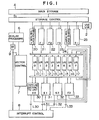
- FIG. 1 showing the general arrangement of the inventive vector processing apparatus
- the unit 6 activates the vector processing controller 7 with the indication of the vector instruction starting address, the number of elements of vector processing, and the mode of processing (parallel or single).
- the vector processing controller 7 reads a vector instruction in the storage 4 according to the starting address indicated, analyzes the instruction, and then dictates to the vector registers (VRO-VR7) 10-17, memory requesters for fetching vector data (FO-F3) 20-23, memory requesters for storing vector data (SO, Sl) 24 and 25, or pipeline arithmetic units (EO-E3) 30-33, depending on the result of analysis, for the execution of the vector instruction.
- the fetching memory requesters FO-F3 calculate the vector data address in the main storage using the vector address register 2 to read out vector data in the main storage 4 via the storage control unit 5, and transfers the vector data to the vector registers VRO-VR7.
- Each of the vector registers VRO-VR7 can latch vector elements of TMAX in number, and is operable to read and write simultaneously.
- the pipeline arithmetic units EO-E3 perform arithmetic operations for vector data in the vector registers VRO-VR7, and leave the results in the vector registers.
- the storing memory requesters SO and Sl calculate the vector data address in the main storage using the vector address register 2, and transfer vector data in the vector registers VR0-VR7 via the storage control unit 5 to the main storage 4. All of the fetching memory requesters FO-F3, storing memory requesters SO and Sl, and pipeline arithmetic units EO-E3 can operate concurrently. It is a common practice to control the parallel operations of the memory requesters and pipeline arithmetic units to the extent of retaining the legitimacy of data thereby to speed up the vector processing,
- the flag flip-flop 9 is set by the scalar processing unit 6 to indicate the parallel processing mode when the vector processing controller 7 is initiated.
- the flip-flop 9 is set to "1", indicating the parallel processing mode, two of the memory requesters and pipeline arithmetic units are paired to execute one vector instruction, and when the flip-flop 9 is reset to "0", one memory requester or pipeline arithmetic unit is used to execute one vector instruction, the latter being called “single processing mode" as against "parallel processing mode” for the former.
- the interrupt process controller 8 is provided with functions for selecting the highest ranking exception out of exception signals 130-133 detected by the pipeline arithmetic units EO-E3, exception signals (not shown) detected by the memory requesters FO-F3, SO and Sl, and exception signals (not shown) detected by the instruction decoding unit (not shown), all occurring independently during the process of a series of vector instructions, and for sampling and holding necessary exception information from a sourcing arithmetic unit, memory requester or instruction decoding unit.
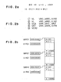
- 1024 elements of vector A are stored at an interval of 7 byte from address 10000
- 1024 elements of vector B are stored at 8-byte interval from address 12000
- 1024 elements of vector C which is the sum of vectors A and B, are stored at 8-byte interval from address 14000.
- Instruction 3 is to add corresponding vector elements loaded in vector registers VRO and VR2, and store the results in the specified vector register VR4.
- Instruction 5 is a control instruction which indicates the end of a vector instruction list and does not concern any virtual vector processing operation.
- 1024 sets of vector elements are added through the four repetitive executions of the vector instruction list shown in Fig. 2b. Each execution cycle will be called "one loop".
- the vector processing controller 7 is provided therein with a register V LR for holding the number of remaining vector elements to be processed.
- the number of remaining elements is more than 256
- 256 sets of vector elements are processed using, for example, the fetching memory requester F0 for the VL instruction in 1, the fetching memory requester Fl for the VL instruction in 2, the arithmetic unit EO for the VEA instruction in 3, and the storing memory requester SO for the VST instruction in 4.
- the VLR contains the initial value subtracted by 256
- the VARO, VAR2 and VAR4 contain each initial value added by VIR x 256. If the esult of decrement of VLR is possitive, the process continues from the top of the vector instruction list using the updated, VARO, VAR2 and VAR4, or if the result becomes negative, the termination process takes place.
- the VL instruction in 1 transfers 256 vector data A(0), A(2), ..., A(510) to the vector register VRO using, for example, the fetching memory requester F0, and 256 vector data A(l), A(3) ..., A(511) to the vector register VR1 using the fetching memory requester Fl.
- the VL instruction in 2 loads even-numbered elements of vector B in the vector register VR2 and odd-numbered elements of vector B in the vector register VR3;
- the VEA instruction in 3 produces in the vector register VR4 the sum of the vector registers VRO and VR2, and in the vector register VR5 the sum of the vector registers VR1 and VR3;
- the VST instruction in 4 stores vector data in the vector register VR4 as resultant vector C(0), C(2), ..., C(510), and vector data in the vector register VR5 as resultant vector C(l), C(3), ..., C(511).
- VLR contains the initial value subtracted by 512 and the VAR contains the initial value added by VIR x 512.
- the process following the result of subtraction for the VLR is identical to the case of single processing mode.
- Fig. 3 shows in block diagram the exception information selecting circuit designed for operating solely in single processing mode. All of memory requesters and pipeline arithmetic units operate to detect exceptions during he execution of a vector instruction. The arrangement for determining the instruction address and element number at which exception has occurred is shown only for the arithmetic units, and the same arrangement for the memory requesters is not shown in the figure.
- the vector process controller 7 analyzes the vector instruction and assigns a pipeline arithmetic unit or memory requester to the instruction if the decision is reached that the vector register specified by the instruction and a pipeline arithmetic unit or memory requester of the type usefull for the instruction are ready for use.
- the vector process controller 7 is provided therein with a register (SIAR) 72 for holding the address of the leading vector instruction and a register (VIAR) 71 for indicating the address of the current instruction.
- register VIAR When the vector process controller 7 is activated, the address of the leading vector instruction indicated by the scalar processing unit 6 is set to register SIAR and, then, to register VIAR. Thereafter, the instruction word length is added to the contents register VIAR through the adder 76 and selector 77 in response to the initiation of the vector instruction. When the VEND instruction is decoded, the leading instruction address held in register SIAR is set to register VIAR. Through the above operation, register VIAR becomes to indicate the address of the initiated vector instruction.
- the vector process controller 7 is provided therein with a register (VER) 70 which indicates the number of vector elements that have been processed so that the leading vector element number to be processed by the initiated instruction is indicated.
- the updating operation for register VER is as follows. Register VER is cleared when the vector process controller 7 is activated. Thereafter, each time the VEND instruction is decoded, the vector register length VMAX is added to the contents of register VER through the adder 78 and selector 79. Through this operation, register - VER can indiate the leading vector element number.
- pipeline arithmetic units 30-33 saves the address of the vector instruction in the register 36 and the leading vector element number in the register 302.
- the vector register internal address counter 301 in each arithmetic unit is set to VMAX.
- the leading vector element number is moved to register 304 and, then, to 305
- the vector instruction address is moved to register 308 and, then, to 309.
- the first vector element reaches the third stage, i.e., the last stage, process for one vector element completes, and the vector register internal address counter 301 is incremented by one through the adder 310 and selector 311 to become "00".
- the counter 301 containing VMAX is incremented by one, it returns to "00" count, indicating the first element.
- the exception detect signal is issued to the interrupt process controller 8, and at the same time the registers 305 and 309 and the vector register internal address counter 301 are disabled from further updating in response to this signal.
- the second and following elements are processed in the same way as in the first element, and unless exception is detected the vector register internal address counter 301 is incremented through the adder 310 and selector each time the process for an element completes.
- the purpose of saving the leading vector element number and vector instruction address in each stage of arithmetic pipeline 300 is the distinction among vector instructions existing concurrently within the arithmetic pipeline 300. For an apparatus of different design where two or more instruction do not exist concurrently in the arithmetic pipeline 300, these registers need not be provided for each stage separately.
- the pipeline arithmetic units 30-33 can find the vector instruction address in the register 309 and the vector element number in the registers 305 and 301 for exception which has been detected first. Since the vector process controller 7 initiates vector instructions in the order of their address and the pipeline arithmetic units 30-33 perform processing in the ascending order of element number, exception which is detected first by the arithmetic unit will be one with the smallest element number and earliest address out of exceptions which can be detected by the pipeline arithmetic units 30-33.
- the interrupt process controller 8 for selecting exception with the smallest element number and earliest address out of exception events indicated successively by a number of pipeline arithmetic units.
- the exception detect signal entry 80 in the interrupt process controller 8 takes one of the detect signals selectively so that a set of exception information is introduced to the interrupt process controller 8.
- the vector instruction address is set through the selector 83 to the register 86, the leading vector element number and vector register address are selected by the selectors 81 and 82, respectively, and added together by the adder 89 and set to the exception element number register 84.
- the contents of register 84 is set to register 85 and the contents of register 86 are set to register 87 unconditionally.
- the register 85 already contains the exception element number and the register 87 already contains the exception instruction address of exception which has been detected earlier, and the contents of registers 84 and 85 are compared by the comparator 90 and the contents of registers 86 and 87 are compared by the comparator 91. If the exception element number in 84 for the newly received exception is smaller than the previous one in 85, the signal line 92 goes "1" and OR gate 93 is enabled to output.
- OR gate 93 is also enabled to output.
- the output of the OR gate 93 causes the register 84 to set its contents to the register 85, and the register 86 to set its contents to the register 87.
- the interrupt process controller 8 receives exception detect signals from the pipeline arithmetic units one after another and selects exception with the smallest vector element number and the earliest instruction address based on the comparison with those of the previously detected exception, whereby exception information of the selected exception such as the exception element number, exception instruction address and interrupt code (not shown) is held in the vector processing apparatus performing computation for vectors with elements more in number than the vector register can store.
- exception information selecting circuit operable solely in single processing mode shown in Fig. 3.
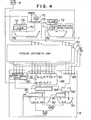
- Fig. 4 differs from that of Fig. 3 in that a selector 73 is provided for switching the count-up value of the processed vector element count register 70 in response to the state of the mode flag flip-flop 9, and in that an exception element number generating circuit 88 is provided for obtaining the exception vector element number given to the register 84, whereas in the arrangement of Fig. 3 this value is obtained by simply adding the outputs of the selectors 81 and 82. Details of the exception element generating circuit 88 will be described later using Fig. 5. The remaining portions of both arrangements of Figs. 3 and 4 are the same.
- the selector 73 selector 73 selects VMAX as the count-up value for VER and the exception element number generating circuit 88 operates as an adder for the outputs of the selectors 81 and 82, and therefore the arrangement works identically to the previous case of Fig. 3.
- the selector 73 selects the duplicate 75 which doubles VMAX, and the exception element number generating circuit 88 operates to modify the vector register address indicated by the pipeline arithmetic units 30-33 and add it to the leading vector element number, whereby exception with the smallest vector element number and the earliest address can be selected, as in the case of single processing mode.
- parallel processing mode As mentioned previously in connection with Fig. 2, a vector instruction is processed by a pair of pipeline arithmetic units in such a way that one is asigned to even-numbered elements and the other assigned to odd-numbered elements, and therefore vector elements of VMAX x 2 in number at maximum are processed in one loop. Accordingly, by summing the contents of processed vector element count register 70 for VMAX x 2 times each time the VEND instruction is decoded, the leading vector element number of vector instruction initiated in one loop can be obtained.
- the pipeline arithmetic units do not directly access to the main storage, and they operate irrespective of the processing mode to indicate to the interrupt process controller 8 the vector register address of a vector element at which exception has been detected.
- the interrupt process controller 8 discriminates as to whether the pipeline arithmetic unit which has detected exception is assigned to even-numbered or odd-numbered elements, and operates on the exception element number generating circuit 88 to add the vector register address multiplied by two in the case of even-numbered elements, or multiplied by two and added by one in the case of odd-numbered elements to the leading vector element number, and set the result to the exception-element number register 84.
- Symbols pp, n, i0-2, 0-7, M-7, e0-3, and 0-7 shown in Fig. 5 correspond to those in the exception element number generating circuit 88.
- the lowest byte of the 4-byte leading element number to be stacked by each pipeline arithmetic unit is always zero, and each unit issues only the high order three bytes (iO-2, 0-7) as the leading element number. Another one byte (l0-7) is needed for indicating the vector register address.
- the signal pp indicates the processing mode
- exception which has occurred first conceptually in dealing with vector elements can readily be selected without impairing the performance of vector instruction execution, whereby infomation on exception comparable with the result of the conventional scalar processing apparatus can be offered to the software system.
Abstract
Description
- The present invention relates to a vector processing apparatus having a plurality of functional facilities capable of operating concurrently and intended to process vectors including elements more in number than the vector register can store.
- There has been proposed a vector processing apparatus having a plurality of vector registers, vector arithmetic units and memory requesters for fetching or storing vector data, and capable of fast vector processing through the concurrent operation of these facilities.
- Such a vector processing apparatus has vector instructions each processing a number of vector elements in the single execution. An example of such vector instructions is the vector addition instruction which adds corresponding elements of vector A(i) and vector B(i). In some cases in executing the vector addition instruction, overflow exception for example, is detected for more than one vector elements. Exceptions which can be detected for each element during the execution of a vector instruction include arithmetic exceptions such as underflow exception, division exception and significance exception, and across exceptions such as address exception, address translation exception and memory protection exception. When such exception is detected, it is not sufficient to notify the software of the type of exception and the instruction address at which the exception has occurred, but it is further necessary to indicate the position of vector element which has caused the exception.
- However, a plurality of vector instructions are executed concurrently in the vector processor and, therefore, a plurality of exceptions can be detected simultaneously. Furthermore, the execution of instructions does not always terminate in the order of instruction address, i.e., exception of a vector instruction at an earlier instruction address can be detected later than exception of a vector instruction at a later instruction address. It would need a complicated process to determine which vector instruction has detected each exception and to perform an interrupt process for each vector instruction, resulting possibly in a degraded overall performance of the apparatus.
- It is an object of the present invention to provide a vector processing apparatus which can readily find out exception that has occurred first conceptually in dealing with vector elements, without impairing the performance of vector instruction execution.
- In a typical form of the invention, each pipeline arithmetic unit is provided with a stack for the leading vector element number, a stack for the vector instruction address and an address counter for the internal use of the vector register, and upon detection of exception by the arithmetic unit, information held in the stack and counter is read out. This information is used to generate the vector element number at which exception has been detected, and the vector element number and instruction address of a newly detected exception are compared with those already held so as to select information of exception to be held ultimately, thereby enabling the determination of exception which has occurred at first in dealing with vector elements.
-
- Fig. 1 is a general block diagram showing the vector processing apparatus embodying the present invention;
- Fig. 2a shows,as an example, the program steps of DO loop in a FORTRAN program;
- Fig. 2b shows a list of vector instructions corersponding to the program show in Fig. 2a;
- Fig. 2c is a description showing vector data in the main storage corresponding to the vector instructions shown in Fig. 2b;
- Fig. 3 is a block diagram showing the exception information selecting circuit in a single processing mode;
- Fig. 4 is a block diagram showing the exception information selecting circuit in a parallel processing mode; and
- Fig. 5 is a schematic diagram showing in detail the exception element number generating circuit shown in Fig. 4.
- An embodiment of the present invention will now be described with reference to the drawings. In Fig. 1 showing the general arrangement of the inventive vector processing apparatus, when the instruction of commencing the process of vector instructions is read out of the
main storage 4 through thestorage control unit 5 to thescalar processing unit 6, theunit 6 activates thevector processing controller 7 with the indication of the vector instruction starting address, the number of elements of vector processing, and the mode of processing (parallel or single). Thevector processing controller 7 reads a vector instruction in thestorage 4 according to the starting address indicated, analyzes the instruction, and then dictates to the vector registers (VRO-VR7) 10-17, memory requesters for fetching vector data (FO-F3) 20-23, memory requesters for storing vector data (SO, Sl) 24 and 25, or pipeline arithmetic units (EO-E3) 30-33, depending on the result of analysis, for the execution of the vector instruction. The fetching memory requesters FO-F3 calculate the vector data address in the main storage using thevector address register 2 to read out vector data in themain storage 4 via thestorage control unit 5, and transfers the vector data to the vector registers VRO-VR7. Each of the vector registers VRO-VR7 can latch vector elements of TMAX in number, and is operable to read and write simultaneously. The pipeline arithmetic units EO-E3 perform arithmetic operations for vector data in the vector registers VRO-VR7, and leave the results in the vector registers. - The storing memory requesters SO and Sl calculate the vector data address in the main storage using the
vector address register 2, and transfer vector data in the vector registers VR0-VR7 via thestorage control unit 5 to themain storage 4. All of the fetching memory requesters FO-F3, storing memory requesters SO and Sl, and pipeline arithmetic units EO-E3 can operate concurrently. It is a common practice to control the parallel operations of the memory requesters and pipeline arithmetic units to the extent of retaining the legitimacy of data thereby to speed up the vector processing, - The flag flip-
flop 9 is set by thescalar processing unit 6 to indicate the parallel processing mode when thevector processing controller 7 is initiated. When the flip-flop 9 is set to "1", indicating the parallel processing mode, two of the memory requesters and pipeline arithmetic units are paired to execute one vector instruction, and when the flip-flop 9 is reset to "0", one memory requester or pipeline arithmetic unit is used to execute one vector instruction, the latter being called "single processing mode" as against "parallel processing mode" for the former. - In the vector processing apparatus, as of this embodiment, where more than one vector instruction is executed concurrently, many exceptions such as, for example, operation exception and specification exception detected during the decoding stage of instruction, access exception detected by the memory requester, and arithmetic exception detected by the arithmetic unit can arise successively. It is rather awkward and less efficient to extract exception information and reexecute the vector instruction by suspending the whole or part of the process at the detection of any exception, and provision of interrupt process for each vector instruction is not always preferrable. Instead, another conceivable method is to run an interrupt process for a series of vector instructions. On this account, the
interrupt process controller 8 is provided with functions for selecting the highest ranking exception out of exception signals 130-133 detected by the pipeline arithmetic units EO-E3, exception signals (not shown) detected by the memory requesters FO-F3, SO and Sl, and exception signals (not shown) detected by the instruction decoding unit (not shown), all occurring independently during the process of a series of vector instructions, and for sampling and holding necessary exception information from a sourcing arithmetic unit, memory requester or instruction decoding unit. - The following describes the process of the vector processing apparatus shown in Fig. 1 dealing with a DO loop of FORTRAN program shown in Fig. 2a. This DO loop is compiled to into vector instructions as shown in Fig. 2b.
Instruction 1 is to load vector A(i), i=0-1023 in vector register VRO;instruction 2 is to load vector B(i), i=0-1023 in vector register VR2; andinstruction 4 is to store vector C(i), i=0-1023 in vector register VR4. VARO, VAR2 and VAR4 are registers holding the starting addresses of areas where the vector data is stored, and VIRO, VIR4 are registers holding the interval of areas storing vector elements. In this example, 1024 elements of vector A are stored at an interval of 7 byte from address 10000, 1024 elements of vector B are stored at 8-byte interval from address 12000, and 1024 elements of vector C, which is the sum of vectors A and B, are stored at 8-byte interval from address 14000.Instruction 3 is to add corresponding vector elements loaded in vector registers VRO and VR2, and store the results in the specified vector register VR4.Instruction 5 is a control instruction which indicates the end of a vector instruction list and does not concern any virtual vector processing operation. - The operation of the apparatus in single processing mode and in parallel processing mode will be described on the assumption that each vector register has a capacity for storing vector elements of VMAX=256. In single processing mode, 1024 sets of vector elements are added through the four repetitive executions of the vector instruction list shown in Fig. 2b. Each execution cycle will be called "one loop". To carry out the cyclic process in a hardware scheme, the
vector processing controller 7 is provided therein with a register VLR for holding the number of remaining vector elements to be processed. In case the number of remaining elements is more than 256, 256 sets of vector elements are processed using, for example, the fetching memory requester F0 for the VL instruction in ①, the fetching memory requester Fl for the VL instruction in ②, the arithmetic unit EO for the VEA instruction in ③, and the storing memory requester SO for the VST instruction in ④. Accordingly, when the VEND instruction is decoded, the VLR contains the initial value subtracted by 256, the VARO, VAR2 and VAR4 contain each initial value added by VIR x 256. If the esult of decrement of VLR is possitive, the process continues from the top of the vector instruction list using the updated, VARO, VAR2 and VAR4, or if the result becomes negative, the termination process takes place. - In parallel processing mode, 1024 sets of vector elements are added through the two repetitive executions of the vector instruction list shown in Fig. 2b. The reduction in execution cycles is made possible through the use of two vector registers, two pipeline arithmetic units and two memory requesters in pair as determined from each vector instruction, that allows 512 sets of vector elements to be processed in one loop. In this mode, the VL instruction in ① transfers 256 vector data A(0), A(2), ..., A(510) to the vector register VRO using, for example, the fetching memory requester F0, and 256 vector data A(l), A(3) ..., A(511) to the vector register VR1 using the fetching memory requester Fl. Subsequently, the VL instruction in ② loads even-numbered elements of vector B in the vector register VR2 and odd-numbered elements of vector B in the vector register VR3; the VEA instruction in ③ produces in the vector register VR4 the sum of the vector registers VRO and VR2, and in the vector register VR5 the sum of the vector registers VR1 and VR3; and the VST instruction in 4 stores vector data in the vector register VR4 as resultant vector C(0), C(2), ..., C(510), and vector data in the vector register VR5 as resultant vector C(l), C(3), ..., C(511). Thus, 512 sets of vector elements are processed in one loop, and when the VEND instruction is decoded the VLR contains the initial value subtracted by 512 and the VAR contains the initial value added by VIR x 512. The process following the result of subtraction for the VLR is identical to the case of single processing mode.
- In order to provide a single interrupt process for a series of vector instructions as shown in Fig. 2b for the example of a DO loop shown in Fig. 2a, it becomes necessary to select one of exceptions that can occur in the DO loop shown in Fig. 2a. Among several priority rules of selection conceivable, such as a rule of ranking operation and specification exceptins higher than access exception and arithmetic exception, a rule of ranking higher an exception related to a vector instruction in the earlier address, a rule of ranking higher an exception related to the smaller vector element number, and so on, this embodiment realizes the rule of selecting at the higher priority an exception related to the smaller element number and, at the same time, related to an instruction at the earlier address. The reason of choosing this priority rule is based on the concept that exception which would be detected earliest in executing a DO loop using scalar instructions should be selected first.
- Fig. 3 shows in block diagram the exception information selecting circuit designed for operating solely in single processing mode. All of memory requesters and pipeline arithmetic units operate to detect exceptions during he execution of a vector instruction. The arrangement for determining the instruction address and element number at which exception has occurred is shown only for the arithmetic units, and the same arrangement for the memory requesters is not shown in the figure.
- In Fig. 3, the
vector process controller 7 analyzes the vector instruction and assigns a pipeline arithmetic unit or memory requester to the instruction if the decision is reached that the vector register specified by the instruction and a pipeline arithmetic unit or memory requester of the type usefull for the instruction are ready for use. Thevector process controller 7 is provided therein with a register (SIAR) 72 for holding the address of the leading vector instruction and a register (VIAR) 71 for indicating the address of the current instruction. - The following describes the updating operation of register VIAR. When the
vector process controller 7 is activated, the address of the leading vector instruction indicated by thescalar processing unit 6 is set to register SIAR and, then, to register VIAR. Thereafter, the instruction word length is added to the contents register VIAR through theadder 76 andselector 77 in response to the initiation of the vector instruction. When the VEND instruction is decoded, the leading instruction address held in register SIAR is set to register VIAR. Through the above operation, register VIAR becomes to indicate the address of the initiated vector instruction. - The
vector process controller 7 is provided therein with a register (VER) 70 which indicates the number of vector elements that have been processed so that the leading vector element number to be processed by the initiated instruction is indicated. The updating operation for register VER is as follows. Register VER is cleared when thevector process controller 7 is activated. Thereafter, each time the VEND instruction is decoded, the vector register length VMAX is added to the contents of register VER through theadder 78 andselector 79. Through this operation, register-VER can indiate the leading vector element number. - Next, the operation for obtaining the vector instruction address and vector element number for exception detected by each pipeline arithmetic unit wil be described. Upon initiation of a vector instruction by the
vector process controller 7, pipeline arithmetic units 30-33 saves the address of the vector instruction in the register 36 and the leading vector element number in the register 302. At initiation of the instruction, the vector registerinternal address counter 301 in each arithmetic unit is set to VMAX. When the first element of vector data to be processed is entered to the first stage of thearithmetic pipeline 300, the contents of register 302 holding the leading vector element number are copied to register 303, and the contents of register 306 holding the vector instruction addrss are copied to register 307. Thereafter, as the data is moved to the second and, then, third stage of thearithmetic pipeline 300, the leading vector element number is moved to register 304 and, then, to 305, and the vector instruction address is moved to register 308 and, then, to 309. When the first vector element reaches the third stage, i.e., the last stage, process for one vector element completes, and the vector registerinternal address counter 301 is incremented by one through theadder 310 andselector 311 to become "00". Namely, when thecounter 301 containing VMAX is incremented by one, it returns to "00" count, indicating the first element. If exception has been detected during the arithmetic process, the exception detect signal is issued to the interruptprocess controller 8, and at the same time theregisters internal address counter 301 are disabled from further updating in response to this signal. - The second and following elements are processed in the same way as in the first element, and unless exception is detected the vector register
internal address counter 301 is incremented through theadder 310 and selector each time the process for an element completes. The purpose of saving the leading vector element number and vector instruction address in each stage ofarithmetic pipeline 300 is the distinction among vector instructions existing concurrently within thearithmetic pipeline 300. For an apparatus of different design where two or more instruction do not exist concurrently in thearithmetic pipeline 300, these registers need not be provided for each stage separately. - Through the above operation, the pipeline arithmetic units 30-33 can find the vector instruction address in the
register 309 and the vector element number in theregisters vector process controller 7 initiates vector instructions in the order of their address and the pipeline arithmetic units 30-33 perform processing in the ascending order of element number, exception which is detected first by the arithmetic unit will be one with the smallest element number and earliest address out of exceptions which can be detected by the pipeline arithmetic units 30-33. - The following describes the operation of the interrupt
process controller 8 for selecting exception with the smallest element number and earliest address out of exception events indicated successively by a number of pipeline arithmetic units. In response to exception detect signals issued by the arithmetic units 30-33, the exception detectsignal entry 80 in the interruptprocess controller 8 takes one of the detect signals selectively so that a set of exception information is introduced to the interruptprocess controller 8. Namely, the vector instruction address is set through theselector 83 to theregister 86, the leading vector element number and vector register address are selected by theselectors 81 and 82, respectively, and added together by the adder 89 and set to the exceptionelement number register 84. In the case of exception which is first received by the interruptprocess controller 8, the contents ofregister 84 is set to register 85 and the contents ofregister 86 are set to register 87 unconditionally. In other case, theregister 85 already contains the exception element number and theregister 87 already contains the exception instruction address of exception which has been detected earlier, and the contents ofregisters comparator 90 and the contents ofregisters comparator 91. If the exception element number in 84 for the newly received exception is smaller than the previous one in 85, the signal line 92 goes "1" andOR gate 93 is enabled to output. If the exception element number of the newly received exception is equal to the previous one and, at the same time, if the exception instruction address in 86 of the newly received exception is earlier than the previous one, ANDgate 94 is enabled to output "1" and then theOR gate 93 is also enabled to output. The output of theOR gate 93 causes theregister 84 to set its contents to theregister 85, and theregister 86 to set its contents to theregister 87. - In this way, the interrupt process controller 8 receives exception detect signals from the pipeline arithmetic units one after another and selects exception with the smallest vector element number and the earliest instruction address based on the comparison with those of the previously detected exception, whereby exception information of the selected exception such as the exception element number, exception instruction address and interrupt code (not shown) is held in the vector processing apparatus performing computation for vectors with elements more in number than the vector register can store. There are the operation of the exception information selecting circuit operable solely in single processing mode shown in Fig. 3.
- Next, the operation of the exception information selecting circuit operable in both the single and parallel processing modes will be described with reference to Fig. 4. The arrangement of Fig. 4 differs from that of Fig. 3 in that a
selector 73 is provided for switching the count-up value of the processed vectorelement count register 70 in response to the state of the mode flag flip-flop 9, and in that an exception elementnumber generating circuit 88 is provided for obtaining the exception vector element number given to theregister 84, whereas in the arrangement of Fig. 3 this value is obtained by simply adding the outputs of theselectors 81 and 82. Details of the exceptionelement generating circuit 88 will be described later using Fig. 5. The remaining portions of both arrangements of Figs. 3 and 4 are the same. - When the mode flag flip-
flop 9 is reset to "0", indicating the single processing mode, theselector 73selector 73 selects VMAX as the count-up value for VER and the exception elementnumber generating circuit 88 operates as an adder for the outputs of theselectors 81 and 82, and therefore the arrangement works identically to the previous case of Fig. 3. When the mode flag flip-flop 9 is set to "1", indicating the parallel processing mode, theselector 73 selects the duplicate 75 which doubles VMAX, and the exception elementnumber generating circuit 88 operates to modify the vector register address indicated by the pipeline arithmetic units 30-33 and add it to the leading vector element number, whereby exception with the smallest vector element number and the earliest address can be selected, as in the case of single processing mode. - The operation specific to parallel processing mode will be described in the following. In parallel processing mode, as mentioned previously in connection with Fig. 2, a vector instruction is processed by a pair of pipeline arithmetic units in such a way that one is asigned to even-numbered elements and the other assigned to odd-numbered elements, and therefore vector elements of VMAX x 2 in number at maximum are processed in one loop. Accordingly, by summing the contents of processed vector
element count register 70 for VMAX x 2 times each time the VEND instruction is decoded, the leading vector element number of vector instruction initiated in one loop can be obtained. The pipeline arithmetic units do not directly access to the main storage, and they operate irrespective of the processing mode to indicate to the interruptprocess controller 8 the vector register address of a vector element at which exception has been detected. The interruptprocess controller 8 discriminates as to whether the pipeline arithmetic unit which has detected exception is assigned to even-numbered or odd-numbered elements, and operates on the exception elementnumber generating circuit 88 to add the vector register address multiplied by two in the case of even-numbered elements, or multiplied by two and added by one in the case of odd-numbered elements to the leading vector element number, and set the result to the exception-element number register 84. - The following describes in detail the exception element
number generating circuit 88 for a particular case of the exceptionelement number register 85 having 4-byte length and the vector register length being VMAX=256, as shown in Fig. 5. Symbols pp, n, i0-2, 0-7, M-7, e0-3, and 0-7 shown in Fig. 5 correspond to those in the exception elementnumber generating circuit 88. The lowest byte of the 4-byte leading element number to be stacked by each pipeline arithmetic unit is always zero, and each unit issues only the high order three bytes (iO-2, 0-7) as the leading element number. Another one byte (ℓ0-7) is needed for indicating the vector register address. The signal pp indicates the processing mode, and the signal line n carries the signal indicating that a pipeline arithmetic unit is assigned to odd-numbered elements. Addition of the leading element number and the vector register address in single processing mode is realized by simply merging i0-2, 0-7 into 10-7. At this time, theshifter 880 received pp=0, and the shift operation does not take place. - Generation of the exception element number in parallel processing mode is carried out in combination of the operation of doubling the vector register internal address indicated by a pipeline arithmetic unit, the operation of adding one to the doubled result in the case of an odd-numbered element, and the operation of adding the result to the leading element number. These operations are carried out using the
shifter 880 andOR gate 881. Namely, in order to modify (duplication and addition by 1) the vector register internal address indicated by a pipeline arithmetic unit, theshifter 880 is arranged for the case of pp=l such that:
- For the addition of the modified vector register internal address to the leading element number, the
shifter 880 is made to provide outputs e30-e37 and, based on i27=0 always in parallel processing mode, an ORgate 881 is provided to obtain e27. Thus, the exception elementnumber generating circuit 88 for the case of VMAX=256 can be realized by a relatively simple circuit arrangement as shown in Fig. 5. - According to the present invention, exception which has occurred first conceptually in dealing with vector elements can readily be selected without impairing the performance of vector instruction execution, whereby infomation on exception comparable with the result of the conventional scalar processing apparatus can be offered to the software system.
Claims (4)
Applications Claiming Priority (2)
| Application Number | Priority Date | Filing Date | Title |
|---|---|---|---|
| JP243943/83 | 1983-12-26 | ||
| JP58243943A JPS60136872A (en) | 1983-12-26 | 1983-12-26 | Vector processor |
Publications (3)
| Publication Number | Publication Date |
|---|---|
| EP0147858A2 true EP0147858A2 (en) | 1985-07-10 |
| EP0147858A3 EP0147858A3 (en) | 1988-04-20 |
| EP0147858B1 EP0147858B1 (en) | 1991-09-25 |
Family
ID=17111339
Family Applications (1)
| Application Number | Title | Priority Date | Filing Date |
|---|---|---|---|
| EP84116394A Expired EP0147858B1 (en) | 1983-12-26 | 1984-12-27 | Vector processing apparatus |
Country Status (4)
| Country | Link |
|---|---|
| US (1) | US4777593A (en) |
| EP (1) | EP0147858B1 (en) |
| JP (1) | JPS60136872A (en) |
| DE (1) | DE3485119D1 (en) |
Cited By (5)
| Publication number | Priority date | Publication date | Assignee | Title |
|---|---|---|---|---|
| EP0297893A2 (en) * | 1987-07-01 | 1989-01-04 | Digital Equipment Corporation | Apparatus and method for recovering from page faults in vector data processing operations |
| EP0333365A2 (en) * | 1988-03-18 | 1989-09-20 | Digital Equipment Corporation | Method and apparatus for handling asynchronous memory management exceptions by a vector processor |
| EP0407911A2 (en) * | 1989-07-07 | 1991-01-16 | Hitachi, Ltd. | Parallel processing apparatus and parallel processing method |
| GB2339623A (en) * | 1998-05-14 | 2000-02-02 | Advanced Risc Mach Ltd | Handling exceptions occurring during processing of vector instructions |
| US6256726B1 (en) | 1988-11-11 | 2001-07-03 | Hitachi, Ltd. | Data processor for the parallel processing of a plurality of instructions |
Families Citing this family (29)
| Publication number | Priority date | Publication date | Assignee | Title |
|---|---|---|---|---|
| JPH0769783B2 (en) * | 1987-11-16 | 1995-07-31 | 日本電気株式会社 | Exception handling method |
| US5367654A (en) * | 1988-04-13 | 1994-11-22 | Hitachi Ltd. | Method and apparatus for controlling storage in computer system utilizing forecasted access requests and priority decision circuitry |
| US4935849A (en) * | 1988-05-16 | 1990-06-19 | Stardent Computer, Inc. | Chaining and hazard apparatus and method |
| US4969117A (en) * | 1988-05-16 | 1990-11-06 | Ardent Computer Corporation | Chaining and hazard apparatus and method |
| JP3076044B2 (en) * | 1988-07-27 | 2000-08-14 | 日本電気株式会社 | Error information storage method for pipeline |
| EP0365322A3 (en) * | 1988-10-19 | 1991-11-27 | Hewlett-Packard Company | Method and apparatus for exception handling in pipeline processors having mismatched instruction pipeline depths |
| JP2607689B2 (en) * | 1989-07-10 | 1997-05-07 | 株式会社日立製作所 | Vector processing equipment |
| US5197138A (en) * | 1989-12-26 | 1993-03-23 | Digital Equipment Corporation | Reporting delayed coprocessor exceptions to code threads having caused the exceptions by saving and restoring exception state during code thread switching |
| US5119324A (en) * | 1990-02-20 | 1992-06-02 | Stardent Computer | Apparatus and method for performing arithmetic functions in a computer system |
| US5053986A (en) * | 1990-02-21 | 1991-10-01 | Stardent Computer, Inc. | Circuit for preservation of sign information in operations for comparison of the absolute value of operands |
| US5206952A (en) * | 1990-09-12 | 1993-04-27 | Cray Research, Inc. | Fault tolerant networking architecture |
| US5392443A (en) * | 1991-03-19 | 1995-02-21 | Hitachi, Ltd. | Vector processor with a memory assigned with skewed addresses adapted for concurrent fetching of a number of vector elements belonging to the same vector data |
| JP2925818B2 (en) * | 1991-04-05 | 1999-07-28 | 株式会社東芝 | Parallel processing controller |
| JPH04336378A (en) * | 1991-05-14 | 1992-11-24 | Nec Corp | Information processor |
| US5761407A (en) * | 1993-03-15 | 1998-06-02 | International Business Machines Corporation | Message based exception handler |
| DE4434895C2 (en) * | 1993-12-23 | 1998-12-24 | Hewlett Packard Co | Method and device for handling exceptional conditions |
| EP0681236B1 (en) * | 1994-05-05 | 2000-11-22 | Conexant Systems, Inc. | Space vector data path |
| JP3495173B2 (en) * | 1996-02-14 | 2004-02-09 | 富士通株式会社 | Arithmetic processing method and arithmetic processing device |
| US9411584B2 (en) * | 2012-12-29 | 2016-08-09 | Intel Corporation | Methods, apparatus, instructions, and logic to provide vector address conflict detection functionality |
| US9823924B2 (en) | 2013-01-23 | 2017-11-21 | International Business Machines Corporation | Vector element rotate and insert under mask instruction |
| US9471308B2 (en) | 2013-01-23 | 2016-10-18 | International Business Machines Corporation | Vector floating point test data class immediate instruction |
| US9804840B2 (en) | 2013-01-23 | 2017-10-31 | International Business Machines Corporation | Vector Galois Field Multiply Sum and Accumulate instruction |
| US9715385B2 (en) * | 2013-01-23 | 2017-07-25 | International Business Machines Corporation | Vector exception code |
| US9778932B2 (en) | 2013-01-23 | 2017-10-03 | International Business Machines Corporation | Vector generate mask instruction |
| US9513906B2 (en) | 2013-01-23 | 2016-12-06 | International Business Machines Corporation | Vector checksum instruction |
| US10338920B2 (en) | 2015-12-18 | 2019-07-02 | Intel Corporation | Instructions and logic for get-multiple-vector-elements operations |
| US20170177351A1 (en) * | 2015-12-18 | 2017-06-22 | Intel Corporation | Instructions and Logic for Even and Odd Vector Get Operations |
| GB2546510B (en) * | 2016-01-20 | 2018-09-26 | Advanced Risc Mach Ltd | Vector atomic memory update instruction |
| US10216515B2 (en) * | 2016-10-18 | 2019-02-26 | Oracle International Corporation | Processor load using a bit vector to calculate effective address |
Citations (2)
| Publication number | Priority date | Publication date | Assignee | Title |
|---|---|---|---|---|
| JPS5897770A (en) * | 1981-12-04 | 1983-06-10 | Fujitsu Ltd | Access controlling system for vector instruction |
| EP0141232A2 (en) * | 1983-10-24 | 1985-05-15 | International Business Machines Corporation | Vector processing unit |
Family Cites Families (10)
| Publication number | Priority date | Publication date | Assignee | Title |
|---|---|---|---|---|
| US4025771A (en) * | 1974-03-25 | 1977-05-24 | Hughes Aircraft Company | Pipe line high speed signal processor |
| US4101960A (en) * | 1977-03-29 | 1978-07-18 | Burroughs Corporation | Scientific processor |
| JPS6024985B2 (en) * | 1978-08-31 | 1985-06-15 | 富士通株式会社 | Data processing method |
| JPS55110340A (en) * | 1979-02-16 | 1980-08-25 | Fujitsu Ltd | Data processing system |
| US4302818A (en) * | 1979-07-10 | 1981-11-24 | Texas Instruments Incorporated | Micro-vector processor |
| US4298936A (en) * | 1979-11-15 | 1981-11-03 | Analogic Corporation | Array Processor |
| JPS5688560A (en) * | 1979-12-21 | 1981-07-18 | Fujitsu Ltd | Vector arithmetic unit |
| JPS6019032B2 (en) * | 1979-12-26 | 1985-05-14 | 富士通株式会社 | Vector arithmetic processing unit |
| US4338675A (en) * | 1980-02-13 | 1982-07-06 | Intel Corporation | Numeric data processor |
| JPS57134774A (en) * | 1981-02-13 | 1982-08-20 | Hitachi Ltd | Vector operating device |
-
1983
- 1983-12-26 JP JP58243943A patent/JPS60136872A/en active Granted
-
1984
- 1984-12-21 US US06/685,112 patent/US4777593A/en not_active Expired - Fee Related
- 1984-12-27 DE DE8484116394T patent/DE3485119D1/en not_active Expired - Lifetime
- 1984-12-27 EP EP84116394A patent/EP0147858B1/en not_active Expired
Patent Citations (2)
| Publication number | Priority date | Publication date | Assignee | Title |
|---|---|---|---|---|
| JPS5897770A (en) * | 1981-12-04 | 1983-06-10 | Fujitsu Ltd | Access controlling system for vector instruction |
| EP0141232A2 (en) * | 1983-10-24 | 1985-05-15 | International Business Machines Corporation | Vector processing unit |
Non-Patent Citations (4)
| Title |
|---|
| IBM TECHNICAL DISCLOSURE BULLETIN, vol. 24, no. 11A, April 1982, page 5530, New York, US; S.P. DALE et al.: "Pipeline processor exception control mechanism" * |
| IBM TECHNICAL DISCLOSURE BULLETIN, vol. 25, no. 1, June 1982, pages 121-123, New York, US; A.G. LILES et al.: "Interruption scheme for vector instructions" * |
| IBM TECHNICAL DISCLOSURE BULLETIN, vol. 25, no. 12, May 1983, pages 6711-6712, New-York, US; L.C. GARCIA et al.: "Storage access-exception detection for pipelined execution units" * |
| PATENT ABSTRACTS OF JAPAN, vol. 7, no. 198 (P-220)[1343], 2nd September 1983; & JP-A-58 97 770 (FUJITSU K.K.) 10-06-1983 * |
Cited By (13)
| Publication number | Priority date | Publication date | Assignee | Title |
|---|---|---|---|---|
| EP0297893A3 (en) * | 1987-07-01 | 1992-01-22 | Digital Equipment Corporation | Apparatus and method for recovering from page faults in vector data processing operations |
| EP0297893A2 (en) * | 1987-07-01 | 1989-01-04 | Digital Equipment Corporation | Apparatus and method for recovering from page faults in vector data processing operations |
| EP0333365A2 (en) * | 1988-03-18 | 1989-09-20 | Digital Equipment Corporation | Method and apparatus for handling asynchronous memory management exceptions by a vector processor |
| EP0333365A3 (en) * | 1988-03-18 | 1991-05-08 | Digital Equipment Corporation | Method and apparatus for handling asynchronous memory management exceptions by a vector processor |
| US6256726B1 (en) | 1988-11-11 | 2001-07-03 | Hitachi, Ltd. | Data processor for the parallel processing of a plurality of instructions |
| US7424598B2 (en) | 1988-11-11 | 2008-09-09 | Renesas Technology Corp. | Data processor |
| EP0407911A3 (en) * | 1989-07-07 | 1992-10-14 | Hitachi, Ltd. | Parallel processing apparatus and parallel processing method |
| US5287465A (en) * | 1989-07-07 | 1994-02-15 | Hitachi, Ltd. | Parallel processing apparatus and method capable of switching parallel and successive processing modes |
| US5561775A (en) * | 1989-07-07 | 1996-10-01 | Hitachi, Ltd. | Parallel processing apparatus and method capable of processing plural instructions in parallel or successively |
| EP0407911A2 (en) * | 1989-07-07 | 1991-01-16 | Hitachi, Ltd. | Parallel processing apparatus and parallel processing method |
| GB2339623A (en) * | 1998-05-14 | 2000-02-02 | Advanced Risc Mach Ltd | Handling exceptions occurring during processing of vector instructions |
| US6304963B1 (en) | 1998-05-14 | 2001-10-16 | Arm Limited | Handling exceptions occuring during processing of vector instructions |
| GB2339623B (en) * | 1998-05-14 | 2002-09-25 | Advanced Risc Mach Ltd | Handling exceptions occurring during processing of vector instructions |
Also Published As
| Publication number | Publication date |
|---|---|
| US4777593A (en) | 1988-10-11 |
| EP0147858B1 (en) | 1991-09-25 |
| JPS60136872A (en) | 1985-07-20 |
| EP0147858A3 (en) | 1988-04-20 |
| DE3485119D1 (en) | 1991-10-31 |
| JPH0562390B2 (en) | 1993-09-08 |
Similar Documents
| Publication | Publication Date | Title |
|---|---|---|
| EP0147858A2 (en) | Vector processing apparatus | |
| US6564314B1 (en) | Computer instruction compression | |
| EP0297893B1 (en) | Apparatus and method for recovering from page faults in vector data processing operations | |
| EP0378830B1 (en) | Method and apparatus for handling multiple condition codes as for a parallel pipeline computer | |
| JP3983857B2 (en) | Single instruction multiple data processing using multiple banks of vector registers | |
| US5581721A (en) | Data processing unit which can access more registers than the registers indicated by the register fields in an instruction | |
| US4745547A (en) | Vector processing | |
| US4449184A (en) | Extended address, single and multiple bit microprocessor | |
| EP0240032A2 (en) | Vector processor with vector data compression/expansion capability | |
| US4882701A (en) | Lookahead program loop controller with register and memory for storing number of loop times for branch on count instructions | |
| JPS5931734B2 (en) | central processing unit that executes instructions with special operand specifiers | |
| JPS5911943B2 (en) | Trap mechanism for data processing equipment | |
| US4773035A (en) | Pipelined data processing system utilizing ideal floating point execution condition detection | |
| EP0173040B1 (en) | Vector processing system | |
| CN1151047A (en) | Method of loading instructions into instruction cache | |
| US5297266A (en) | Apparatus and method for controlling memory requests in an information processor | |
| US5642523A (en) | Microprocessor with variable size register windowing | |
| EP0061586B1 (en) | Data processing apparatus with extended general purpose registers | |
| US5729723A (en) | Data processing unit | |
| US6223275B1 (en) | Microprocessor with reduced instruction set limiting the address space to upper 2 Mbytes and executing a long type register branch instruction in three intermediate instructions | |
| US20080215859A1 (en) | Computer with high-speed context switching | |
| US5276767A (en) | Fuzzy computer | |
| IE79236B1 (en) | Apparatus and method for recovering from page faults in vector data processing operations | |
| EP0689129B1 (en) | Processing of computer instructions with a reduced number of bits for operand specifiers | |
| JPH07110769A (en) | Vliw type computer |
Legal Events
| Date | Code | Title | Description |
|---|---|---|---|
| PUAI | Public reference made under article 153(3) epc to a published international application that has entered the european phase |
Free format text: ORIGINAL CODE: 0009012 |
|
| AK | Designated contracting states |
Designated state(s): DE FR GB |
|
| PUAL | Search report despatched |
Free format text: ORIGINAL CODE: 0009013 |
|
| AK | Designated contracting states |
Kind code of ref document: A3 Designated state(s): DE FR GB |
|
| 17P | Request for examination filed |
Effective date: 19880421 |
|
| 17Q | First examination report despatched |
Effective date: 19891023 |
|
| GRAA | (expected) grant |
Free format text: ORIGINAL CODE: 0009210 |
|
| AK | Designated contracting states |
Kind code of ref document: B1 Designated state(s): DE FR GB |
|
| REF | Corresponds to: |
Ref document number: 3485119 Country of ref document: DE Date of ref document: 19911031 |
|
| ET | Fr: translation filed | ||
| PLBE | No opposition filed within time limit |
Free format text: ORIGINAL CODE: 0009261 |
|
| STAA | Information on the status of an ep patent application or granted ep patent |
Free format text: STATUS: NO OPPOSITION FILED WITHIN TIME LIMIT |
|
| 26N | No opposition filed | ||
| PGFP | Annual fee paid to national office [announced via postgrant information from national office to epo] |
Ref country code: FR Payment date: 19971017 Year of fee payment: 14 |
|
| PGFP | Annual fee paid to national office [announced via postgrant information from national office to epo] |
Ref country code: GB Payment date: 19971217 Year of fee payment: 14 |
|
| PGFP | Annual fee paid to national office [announced via postgrant information from national office to epo] |
Ref country code: DE Payment date: 19980227 Year of fee payment: 14 |
|
| PG25 | Lapsed in a contracting state [announced via postgrant information from national office to epo] |
Ref country code: GB Free format text: LAPSE BECAUSE OF NON-PAYMENT OF DUE FEES Effective date: 19981227 |
|
| GBPC | Gb: european patent ceased through non-payment of renewal fee |
Effective date: 19981227 |
|
| PG25 | Lapsed in a contracting state [announced via postgrant information from national office to epo] |
Ref country code: FR Free format text: LAPSE BECAUSE OF NON-PAYMENT OF DUE FEES Effective date: 19990831 |
|
| REG | Reference to a national code |
Ref country code: FR Ref legal event code: ST |
|
| PG25 | Lapsed in a contracting state [announced via postgrant information from national office to epo] |
Ref country code: DE Free format text: LAPSE BECAUSE OF NON-PAYMENT OF DUE FEES Effective date: 19991001 |