EP0152605A1 - High repetition rate, uniform volume transverse electric discharger laser with pulse triggered multi-arc channel switching - Google Patents
High repetition rate, uniform volume transverse electric discharger laser with pulse triggered multi-arc channel switching Download PDFInfo
- Publication number
- EP0152605A1 EP0152605A1 EP84115729A EP84115729A EP0152605A1 EP 0152605 A1 EP0152605 A1 EP 0152605A1 EP 84115729 A EP84115729 A EP 84115729A EP 84115729 A EP84115729 A EP 84115729A EP 0152605 A1 EP0152605 A1 EP 0152605A1
- Authority
- EP
- European Patent Office
- Prior art keywords
- electrode
- laser
- rail
- electrodes
- anode
- Prior art date
- Legal status (The legal status is an assumption and is not a legal conclusion. Google has not performed a legal analysis and makes no representation as to the accuracy of the status listed.)
- Withdrawn
Links
- 230000001960 triggered effect Effects 0.000 title claims description 16
- 230000015556 catabolic process Effects 0.000 claims description 28
- 239000007788 liquid Substances 0.000 claims description 13
- 230000000630 rising effect Effects 0.000 claims description 10
- 239000003990 capacitor Substances 0.000 claims description 8
- 229910052751 metal Inorganic materials 0.000 claims description 8
- 239000002184 metal Substances 0.000 claims description 8
- 238000011144 upstream manufacturing Methods 0.000 claims description 6
- 238000010276 construction Methods 0.000 claims description 3
- 230000002441 reversible effect Effects 0.000 claims description 2
- 239000012530 fluid Substances 0.000 claims 2
- 238000000137 annealing Methods 0.000 abstract description 26
- 235000012431 wafers Nutrition 0.000 abstract description 25
- 239000004065 semiconductor Substances 0.000 abstract description 8
- 235000021251 pulses Nutrition 0.000 description 73
- 239000007789 gas Substances 0.000 description 65
- XUIMIQQOPSSXEZ-UHFFFAOYSA-N Silicon Chemical compound [Si] XUIMIQQOPSSXEZ-UHFFFAOYSA-N 0.000 description 28
- 229910052710 silicon Inorganic materials 0.000 description 25
- 239000010703 silicon Substances 0.000 description 25
- 238000000034 method Methods 0.000 description 22
- 238000004519 manufacturing process Methods 0.000 description 20
- 239000002019 doping agent Substances 0.000 description 14
- 238000002513 implantation Methods 0.000 description 11
- 239000000463 material Substances 0.000 description 11
- 230000008569 process Effects 0.000 description 11
- 239000000203 mixture Substances 0.000 description 10
- 230000005284 excitation Effects 0.000 description 9
- 229910021421 monocrystalline silicon Inorganic materials 0.000 description 9
- XLYOFNOQVPJJNP-UHFFFAOYSA-N water Chemical compound O XLYOFNOQVPJJNP-UHFFFAOYSA-N 0.000 description 9
- PXHVJJICTQNCMI-UHFFFAOYSA-N Nickel Chemical compound [Ni] PXHVJJICTQNCMI-UHFFFAOYSA-N 0.000 description 8
- 229910021420 polycrystalline silicon Inorganic materials 0.000 description 6
- 230000005855 radiation Effects 0.000 description 5
- ZOXJGFHDIHLPTG-UHFFFAOYSA-N Boron Chemical compound [B] ZOXJGFHDIHLPTG-UHFFFAOYSA-N 0.000 description 4
- OKTJSMMVPCPJKN-UHFFFAOYSA-N Carbon Chemical compound [C] OKTJSMMVPCPJKN-UHFFFAOYSA-N 0.000 description 4
- 235000010627 Phaseolus vulgaris Nutrition 0.000 description 4
- 244000046052 Phaseolus vulgaris Species 0.000 description 4
- 229910021417 amorphous silicon Inorganic materials 0.000 description 4
- 230000015572 biosynthetic process Effects 0.000 description 4
- 229910052796 boron Inorganic materials 0.000 description 4
- 230000008859 change Effects 0.000 description 4
- 238000010961 commercial manufacture process Methods 0.000 description 4
- 230000008878 coupling Effects 0.000 description 4
- 238000010168 coupling process Methods 0.000 description 4
- 238000005859 coupling reaction Methods 0.000 description 4
- 230000005684 electric field Effects 0.000 description 4
- MUJOIMFVNIBMKC-UHFFFAOYSA-N fludioxonil Chemical compound C=12OC(F)(F)OC2=CC=CC=1C1=CNC=C1C#N MUJOIMFVNIBMKC-UHFFFAOYSA-N 0.000 description 4
- 230000004907 flux Effects 0.000 description 4
- 229910002804 graphite Inorganic materials 0.000 description 4
- 239000010439 graphite Substances 0.000 description 4
- 150000004820 halides Chemical class 0.000 description 4
- 229910052736 halogen Inorganic materials 0.000 description 4
- 150000002367 halogens Chemical class 0.000 description 4
- 229910052759 nickel Inorganic materials 0.000 description 4
- 239000010979 ruby Substances 0.000 description 4
- 229910001750 ruby Inorganic materials 0.000 description 4
- 229910001220 stainless steel Inorganic materials 0.000 description 4
- 239000010935 stainless steel Substances 0.000 description 4
- 229910052785 arsenic Inorganic materials 0.000 description 3
- RQNWIZPPADIBDY-UHFFFAOYSA-N arsenic atom Chemical compound [As] RQNWIZPPADIBDY-UHFFFAOYSA-N 0.000 description 3
- 230000005540 biological transmission Effects 0.000 description 3
- 239000013078 crystal Substances 0.000 description 3
- 230000003628 erosive effect Effects 0.000 description 3
- 238000010438 heat treatment Methods 0.000 description 3
- 230000001965 increasing effect Effects 0.000 description 3
- 238000005468 ion implantation Methods 0.000 description 3
- 150000002500 ions Chemical class 0.000 description 3
- 238000005224 laser annealing Methods 0.000 description 3
- 230000003134 recirculating effect Effects 0.000 description 3
- WFKWXMTUELFFGS-UHFFFAOYSA-N tungsten Chemical compound [W] WFKWXMTUELFFGS-UHFFFAOYSA-N 0.000 description 3
- 229910052721 tungsten Inorganic materials 0.000 description 3
- 239000010937 tungsten Substances 0.000 description 3
- XKRFYHLGVUSROY-UHFFFAOYSA-N Argon Chemical compound [Ar] XKRFYHLGVUSROY-UHFFFAOYSA-N 0.000 description 2
- IJGRMHOSHXDMSA-UHFFFAOYSA-N Atomic nitrogen Chemical compound N#N IJGRMHOSHXDMSA-UHFFFAOYSA-N 0.000 description 2
- 229910001369 Brass Inorganic materials 0.000 description 2
- VEXZGXHMUGYJMC-UHFFFAOYSA-N Hydrochloric acid Chemical compound Cl VEXZGXHMUGYJMC-UHFFFAOYSA-N 0.000 description 2
- ZOKXTWBITQBERF-UHFFFAOYSA-N Molybdenum Chemical compound [Mo] ZOKXTWBITQBERF-UHFFFAOYSA-N 0.000 description 2
- 229910052782 aluminium Inorganic materials 0.000 description 2
- XAGFODPZIPBFFR-UHFFFAOYSA-N aluminium Chemical compound [Al] XAGFODPZIPBFFR-UHFFFAOYSA-N 0.000 description 2
- 239000010951 brass Substances 0.000 description 2
- 238000009792 diffusion process Methods 0.000 description 2
- 238000010894 electron beam technology Methods 0.000 description 2
- 239000001307 helium Substances 0.000 description 2
- 229910052734 helium Inorganic materials 0.000 description 2
- SWQJXJOGLNCZEY-UHFFFAOYSA-N helium atom Chemical compound [He] SWQJXJOGLNCZEY-UHFFFAOYSA-N 0.000 description 2
- BHEPBYXIRTUNPN-UHFFFAOYSA-N hydridophosphorus(.) (triplet) Chemical compound [PH] BHEPBYXIRTUNPN-UHFFFAOYSA-N 0.000 description 2
- 239000007943 implant Substances 0.000 description 2
- 239000012535 impurity Substances 0.000 description 2
- 230000000670 limiting effect Effects 0.000 description 2
- 239000007791 liquid phase Substances 0.000 description 2
- 229910001507 metal halide Inorganic materials 0.000 description 2
- 150000005309 metal halides Chemical class 0.000 description 2
- 229910052750 molybdenum Inorganic materials 0.000 description 2
- 239000011733 molybdenum Substances 0.000 description 2
- 230000003287 optical effect Effects 0.000 description 2
- 238000005086 pumping Methods 0.000 description 2
- 230000008439 repair process Effects 0.000 description 2
- 229910052715 tantalum Inorganic materials 0.000 description 2
- GUVRBAGPIYLISA-UHFFFAOYSA-N tantalum atom Chemical compound [Ta] GUVRBAGPIYLISA-UHFFFAOYSA-N 0.000 description 2
- BQCIDUSAKPWEOX-UHFFFAOYSA-N 1,1-Difluoroethene Chemical compound FC(F)=C BQCIDUSAKPWEOX-UHFFFAOYSA-N 0.000 description 1
- KXGFMDJXCMQABM-UHFFFAOYSA-N 2-methoxy-6-methylphenol Chemical compound [CH]OC1=CC=CC([CH])=C1O KXGFMDJXCMQABM-UHFFFAOYSA-N 0.000 description 1
- VXEGSRKPIUDPQT-UHFFFAOYSA-N 4-[4-(4-methoxyphenyl)piperazin-1-yl]aniline Chemical compound C1=CC(OC)=CC=C1N1CCN(C=2C=CC(N)=CC=2)CC1 VXEGSRKPIUDPQT-UHFFFAOYSA-N 0.000 description 1
- MARUHZGHZWCEQU-UHFFFAOYSA-N 5-phenyl-2h-tetrazole Chemical compound C1=CC=CC=C1C1=NNN=N1 MARUHZGHZWCEQU-UHFFFAOYSA-N 0.000 description 1
- JBRZTFJDHDCESZ-UHFFFAOYSA-N AsGa Chemical compound [As]#[Ga] JBRZTFJDHDCESZ-UHFFFAOYSA-N 0.000 description 1
- WKBOTKDWSSQWDR-UHFFFAOYSA-N Bromine atom Chemical compound [Br] WKBOTKDWSSQWDR-UHFFFAOYSA-N 0.000 description 1
- ZAMOUSCENKQFHK-UHFFFAOYSA-N Chlorine atom Chemical compound [Cl] ZAMOUSCENKQFHK-UHFFFAOYSA-N 0.000 description 1
- RYGMFSIKBFXOCR-UHFFFAOYSA-N Copper Chemical compound [Cu] RYGMFSIKBFXOCR-UHFFFAOYSA-N 0.000 description 1
- QPLDLSVMHZLSFG-UHFFFAOYSA-N Copper oxide Chemical compound [Cu]=O QPLDLSVMHZLSFG-UHFFFAOYSA-N 0.000 description 1
- 239000005751 Copper oxide Substances 0.000 description 1
- LFQSCWFLJHTTHZ-UHFFFAOYSA-N Ethanol Chemical compound CCO LFQSCWFLJHTTHZ-UHFFFAOYSA-N 0.000 description 1
- PXGOKWXKJXAPGV-UHFFFAOYSA-N Fluorine Chemical compound FF PXGOKWXKJXAPGV-UHFFFAOYSA-N 0.000 description 1
- 229910005540 GaP Inorganic materials 0.000 description 1
- 229910001218 Gallium arsenide Inorganic materials 0.000 description 1
- GPXJNWSHGFTCBW-UHFFFAOYSA-N Indium phosphide Chemical compound [In]#P GPXJNWSHGFTCBW-UHFFFAOYSA-N 0.000 description 1
- 229920006370 Kynar Polymers 0.000 description 1
- VVQNEPGJFQJSBK-UHFFFAOYSA-N Methyl methacrylate Chemical compound COC(=O)C(C)=C VVQNEPGJFQJSBK-UHFFFAOYSA-N 0.000 description 1
- OAICVXFJPJFONN-UHFFFAOYSA-N Phosphorus Chemical compound [P] OAICVXFJPJFONN-UHFFFAOYSA-N 0.000 description 1
- 229920005372 Plexiglas® Polymers 0.000 description 1
- 229910018503 SF6 Inorganic materials 0.000 description 1
- 229910003910 SiCl4 Inorganic materials 0.000 description 1
- 238000010521 absorption reaction Methods 0.000 description 1
- LVQULNGDVIKLPK-UHFFFAOYSA-N aluminium antimonide Chemical compound [Sb]#[Al] LVQULNGDVIKLPK-UHFFFAOYSA-N 0.000 description 1
- PNEYBMLMFCGWSK-UHFFFAOYSA-N aluminium oxide Inorganic materials [O-2].[O-2].[O-2].[Al+3].[Al+3] PNEYBMLMFCGWSK-UHFFFAOYSA-N 0.000 description 1
- 229910052786 argon Inorganic materials 0.000 description 1
- 230000008901 benefit Effects 0.000 description 1
- GDTBXPJZTBHREO-UHFFFAOYSA-N bromine Substances BrBr GDTBXPJZTBHREO-UHFFFAOYSA-N 0.000 description 1
- 229910052794 bromium Inorganic materials 0.000 description 1
- CJOBVZJTOIVNNF-UHFFFAOYSA-N cadmium sulfide Chemical compound [Cd]=S CJOBVZJTOIVNNF-UHFFFAOYSA-N 0.000 description 1
- 229910052980 cadmium sulfide Inorganic materials 0.000 description 1
- 238000007600 charging Methods 0.000 description 1
- 238000006243 chemical reaction Methods 0.000 description 1
- 239000000460 chlorine Substances 0.000 description 1
- 229910052801 chlorine Inorganic materials 0.000 description 1
- RCTYPNKXASFOBE-UHFFFAOYSA-M chloromercury Chemical compound [Hg]Cl RCTYPNKXASFOBE-UHFFFAOYSA-M 0.000 description 1
- 230000001427 coherent effect Effects 0.000 description 1
- 238000007796 conventional method Methods 0.000 description 1
- 238000001816 cooling Methods 0.000 description 1
- 229910052802 copper Inorganic materials 0.000 description 1
- 239000010949 copper Substances 0.000 description 1
- 229910000431 copper oxide Inorganic materials 0.000 description 1
- 230000007547 defect Effects 0.000 description 1
- 230000007812 deficiency Effects 0.000 description 1
- 238000006731 degradation reaction Methods 0.000 description 1
- 238000013461 design Methods 0.000 description 1
- 238000010586 diagram Methods 0.000 description 1
- 239000003989 dielectric material Substances 0.000 description 1
- 230000008034 disappearance Effects 0.000 description 1
- 239000012153 distilled water Substances 0.000 description 1
- 230000000694 effects Effects 0.000 description 1
- 238000010891 electric arc Methods 0.000 description 1
- 238000004146 energy storage Methods 0.000 description 1
- 238000005516 engineering process Methods 0.000 description 1
- 238000011067 equilibration Methods 0.000 description 1
- 238000010304 firing Methods 0.000 description 1
- 229910052731 fluorine Inorganic materials 0.000 description 1
- 239000011737 fluorine Substances 0.000 description 1
- 239000011888 foil Substances 0.000 description 1
- HZXMRANICFIONG-UHFFFAOYSA-N gallium phosphide Chemical compound [Ga]#P HZXMRANICFIONG-UHFFFAOYSA-N 0.000 description 1
- 229910052732 germanium Inorganic materials 0.000 description 1
- GNPVGFCGXDBREM-UHFFFAOYSA-N germanium atom Chemical compound [Ge] GNPVGFCGXDBREM-UHFFFAOYSA-N 0.000 description 1
- 238000000265 homogenisation Methods 0.000 description 1
- 229910000041 hydrogen chloride Inorganic materials 0.000 description 1
- IXCSERBJSXMMFS-UHFFFAOYSA-N hydrogen chloride Substances Cl.Cl IXCSERBJSXMMFS-UHFFFAOYSA-N 0.000 description 1
- 230000001939 inductive effect Effects 0.000 description 1
- PNDPGZBMCMUPRI-UHFFFAOYSA-N iodine Chemical compound II PNDPGZBMCMUPRI-UHFFFAOYSA-N 0.000 description 1
- 238000010849 ion bombardment Methods 0.000 description 1
- 238000010884 ion-beam technique Methods 0.000 description 1
- 229910052743 krypton Inorganic materials 0.000 description 1
- DNNSSWSSYDEUBZ-UHFFFAOYSA-N krypton atom Chemical compound [Kr] DNNSSWSSYDEUBZ-UHFFFAOYSA-N 0.000 description 1
- 238000012423 maintenance Methods 0.000 description 1
- 238000002844 melting Methods 0.000 description 1
- 230000008018 melting Effects 0.000 description 1
- 210000002445 nipple Anatomy 0.000 description 1
- 229910052757 nitrogen Inorganic materials 0.000 description 1
- 238000009828 non-uniform distribution Methods 0.000 description 1
- 230000003534 oscillatory effect Effects 0.000 description 1
- 230000036961 partial effect Effects 0.000 description 1
- 239000012071 phase Substances 0.000 description 1
- 239000005011 phenolic resin Substances 0.000 description 1
- 229920001568 phenolic resin Polymers 0.000 description 1
- 229910052698 phosphorus Inorganic materials 0.000 description 1
- 239000011574 phosphorus Substances 0.000 description 1
- 230000002028 premature Effects 0.000 description 1
- 230000002035 prolonged effect Effects 0.000 description 1
- 230000001681 protective effect Effects 0.000 description 1
- 238000010278 pulse charging Methods 0.000 description 1
- 230000003252 repetitive effect Effects 0.000 description 1
- 238000011160 research Methods 0.000 description 1
- 229910052702 rhenium Inorganic materials 0.000 description 1
- WUAPFZMCVAUBPE-UHFFFAOYSA-N rhenium atom Chemical compound [Re] WUAPFZMCVAUBPE-UHFFFAOYSA-N 0.000 description 1
- FDNAPBUWERUEDA-UHFFFAOYSA-N silicon tetrachloride Chemical compound Cl[Si](Cl)(Cl)Cl FDNAPBUWERUEDA-UHFFFAOYSA-N 0.000 description 1
- 239000005049 silicon tetrachloride Substances 0.000 description 1
- 239000007787 solid Substances 0.000 description 1
- 239000007790 solid phase Substances 0.000 description 1
- 230000006641 stabilisation Effects 0.000 description 1
- 238000011105 stabilization Methods 0.000 description 1
- 230000000087 stabilizing effect Effects 0.000 description 1
- 230000003068 static effect Effects 0.000 description 1
- 239000000758 substrate Substances 0.000 description 1
- SFZCNBIFKDRMGX-UHFFFAOYSA-N sulfur hexafluoride Chemical compound FS(F)(F)(F)(F)F SFZCNBIFKDRMGX-UHFFFAOYSA-N 0.000 description 1
- 229960000909 sulfur hexafluoride Drugs 0.000 description 1
- 238000012546 transfer Methods 0.000 description 1
- 230000001052 transient effect Effects 0.000 description 1
- 238000007740 vapor deposition Methods 0.000 description 1
- 229910052724 xenon Inorganic materials 0.000 description 1
- FHNFHKCVQCLJFQ-UHFFFAOYSA-N xenon atom Chemical compound [Xe] FHNFHKCVQCLJFQ-UHFFFAOYSA-N 0.000 description 1
Images

Classifications
-
- H—ELECTRICITY
- H01—ELECTRIC ELEMENTS
- H01L—SEMICONDUCTOR DEVICES NOT COVERED BY CLASS H10
- H01L21/00—Processes or apparatus adapted for the manufacture or treatment of semiconductor or solid state devices or of parts thereof
- H01L21/02—Manufacture or treatment of semiconductor devices or of parts thereof
- H01L21/04—Manufacture or treatment of semiconductor devices or of parts thereof the devices having at least one potential-jump barrier or surface barrier, e.g. PN junction, depletion layer or carrier concentration layer
- H01L21/18—Manufacture or treatment of semiconductor devices or of parts thereof the devices having at least one potential-jump barrier or surface barrier, e.g. PN junction, depletion layer or carrier concentration layer the devices having semiconductor bodies comprising elements of Group IV of the Periodic System or AIIIBV compounds with or without impurities, e.g. doping materials
- H01L21/26—Bombardment with radiation
- H01L21/263—Bombardment with radiation with high-energy radiation
- H01L21/268—Bombardment with radiation with high-energy radiation using electromagnetic radiation, e.g. laser radiation
-
- H—ELECTRICITY
- H01—ELECTRIC ELEMENTS
- H01L—SEMICONDUCTOR DEVICES NOT COVERED BY CLASS H10
- H01L31/00—Semiconductor devices sensitive to infrared radiation, light, electromagnetic radiation of shorter wavelength or corpuscular radiation and specially adapted either for the conversion of the energy of such radiation into electrical energy or for the control of electrical energy by such radiation; Processes or apparatus specially adapted for the manufacture or treatment thereof or of parts thereof; Details thereof
- H01L31/18—Processes or apparatus specially adapted for the manufacture or treatment of these devices or of parts thereof
- H01L31/1804—Processes or apparatus specially adapted for the manufacture or treatment of these devices or of parts thereof comprising only elements of Group IV of the Periodic System
-
- H—ELECTRICITY
- H01—ELECTRIC ELEMENTS
- H01L—SEMICONDUCTOR DEVICES NOT COVERED BY CLASS H10
- H01L31/00—Semiconductor devices sensitive to infrared radiation, light, electromagnetic radiation of shorter wavelength or corpuscular radiation and specially adapted either for the conversion of the energy of such radiation into electrical energy or for the control of electrical energy by such radiation; Processes or apparatus specially adapted for the manufacture or treatment thereof or of parts thereof; Details thereof
- H01L31/18—Processes or apparatus specially adapted for the manufacture or treatment of these devices or of parts thereof
- H01L31/186—Particular post-treatment for the devices, e.g. annealing, impurity gettering, short-circuit elimination, recrystallisation
- H01L31/1864—Annealing
-
- H—ELECTRICITY
- H01—ELECTRIC ELEMENTS
- H01L—SEMICONDUCTOR DEVICES NOT COVERED BY CLASS H10
- H01L31/00—Semiconductor devices sensitive to infrared radiation, light, electromagnetic radiation of shorter wavelength or corpuscular radiation and specially adapted either for the conversion of the energy of such radiation into electrical energy or for the control of electrical energy by such radiation; Processes or apparatus specially adapted for the manufacture or treatment thereof or of parts thereof; Details thereof
- H01L31/18—Processes or apparatus specially adapted for the manufacture or treatment of these devices or of parts thereof
- H01L31/1876—Particular processes or apparatus for batch treatment of the devices
-
- H—ELECTRICITY
- H01—ELECTRIC ELEMENTS
- H01S—DEVICES USING THE PROCESS OF LIGHT AMPLIFICATION BY STIMULATED EMISSION OF RADIATION [LASER] TO AMPLIFY OR GENERATE LIGHT; DEVICES USING STIMULATED EMISSION OF ELECTROMAGNETIC RADIATION IN WAVE RANGES OTHER THAN OPTICAL
- H01S3/00—Lasers, i.e. devices using stimulated emission of electromagnetic radiation in the infrared, visible or ultraviolet wave range
- H01S3/02—Constructional details
- H01S3/03—Constructional details of gas laser discharge tubes
- H01S3/036—Means for obtaining or maintaining the desired gas pressure within the tube, e.g. by gettering, replenishing; Means for circulating the gas, e.g. for equalising the pressure within the tube
-
- H—ELECTRICITY
- H01—ELECTRIC ELEMENTS
- H01S—DEVICES USING THE PROCESS OF LIGHT AMPLIFICATION BY STIMULATED EMISSION OF RADIATION [LASER] TO AMPLIFY OR GENERATE LIGHT; DEVICES USING STIMULATED EMISSION OF ELECTROMAGNETIC RADIATION IN WAVE RANGES OTHER THAN OPTICAL
- H01S3/00—Lasers, i.e. devices using stimulated emission of electromagnetic radiation in the infrared, visible or ultraviolet wave range
- H01S3/02—Constructional details
- H01S3/03—Constructional details of gas laser discharge tubes
- H01S3/038—Electrodes, e.g. special shape, configuration or composition
- H01S3/0384—Auxiliary electrodes, e.g. for pre-ionisation or triggering, or particular adaptations therefor
-
- H—ELECTRICITY
- H01—ELECTRIC ELEMENTS
- H01S—DEVICES USING THE PROCESS OF LIGHT AMPLIFICATION BY STIMULATED EMISSION OF RADIATION [LASER] TO AMPLIFY OR GENERATE LIGHT; DEVICES USING STIMULATED EMISSION OF ELECTROMAGNETIC RADIATION IN WAVE RANGES OTHER THAN OPTICAL
- H01S3/00—Lasers, i.e. devices using stimulated emission of electromagnetic radiation in the infrared, visible or ultraviolet wave range
- H01S3/09—Processes or apparatus for excitation, e.g. pumping
- H01S3/097—Processes or apparatus for excitation, e.g. pumping by gas discharge of a gas laser
- H01S3/0971—Processes or apparatus for excitation, e.g. pumping by gas discharge of a gas laser transversely excited
- H01S3/09713—Processes or apparatus for excitation, e.g. pumping by gas discharge of a gas laser transversely excited with auxiliary ionisation, e.g. double discharge excitation
-
- Y—GENERAL TAGGING OF NEW TECHNOLOGICAL DEVELOPMENTS; GENERAL TAGGING OF CROSS-SECTIONAL TECHNOLOGIES SPANNING OVER SEVERAL SECTIONS OF THE IPC; TECHNICAL SUBJECTS COVERED BY FORMER USPC CROSS-REFERENCE ART COLLECTIONS [XRACs] AND DIGESTS
- Y02—TECHNOLOGIES OR APPLICATIONS FOR MITIGATION OR ADAPTATION AGAINST CLIMATE CHANGE
- Y02E—REDUCTION OF GREENHOUSE GAS [GHG] EMISSIONS, RELATED TO ENERGY GENERATION, TRANSMISSION OR DISTRIBUTION
- Y02E10/00—Energy generation through renewable energy sources
- Y02E10/50—Photovoltaic [PV] energy
- Y02E10/547—Monocrystalline silicon PV cells
-
- Y—GENERAL TAGGING OF NEW TECHNOLOGICAL DEVELOPMENTS; GENERAL TAGGING OF CROSS-SECTIONAL TECHNOLOGIES SPANNING OVER SEVERAL SECTIONS OF THE IPC; TECHNICAL SUBJECTS COVERED BY FORMER USPC CROSS-REFERENCE ART COLLECTIONS [XRACs] AND DIGESTS
- Y02—TECHNOLOGIES OR APPLICATIONS FOR MITIGATION OR ADAPTATION AGAINST CLIMATE CHANGE
- Y02P—CLIMATE CHANGE MITIGATION TECHNOLOGIES IN THE PRODUCTION OR PROCESSING OF GOODS
- Y02P70/00—Climate change mitigation technologies in the production process for final industrial or consumer products
- Y02P70/50—Manufacturing or production processes characterised by the final manufactured product
-
- Y—GENERAL TAGGING OF NEW TECHNOLOGICAL DEVELOPMENTS; GENERAL TAGGING OF CROSS-SECTIONAL TECHNOLOGIES SPANNING OVER SEVERAL SECTIONS OF THE IPC; TECHNICAL SUBJECTS COVERED BY FORMER USPC CROSS-REFERENCE ART COLLECTIONS [XRACs] AND DIGESTS
- Y10—TECHNICAL SUBJECTS COVERED BY FORMER USPC
- Y10S—TECHNICAL SUBJECTS COVERED BY FORMER USPC CROSS-REFERENCE ART COLLECTIONS [XRACs] AND DIGESTS
- Y10S117/00—Single-crystal, oriented-crystal, and epitaxy growth processes; non-coating apparatus therefor
- Y10S117/903—Dendrite or web or cage technique
- Y10S117/904—Laser beam
-
- Y—GENERAL TAGGING OF NEW TECHNOLOGICAL DEVELOPMENTS; GENERAL TAGGING OF CROSS-SECTIONAL TECHNOLOGIES SPANNING OVER SEVERAL SECTIONS OF THE IPC; TECHNICAL SUBJECTS COVERED BY FORMER USPC CROSS-REFERENCE ART COLLECTIONS [XRACs] AND DIGESTS
- Y10—TECHNICAL SUBJECTS COVERED BY FORMER USPC
- Y10S—TECHNICAL SUBJECTS COVERED BY FORMER USPC CROSS-REFERENCE ART COLLECTIONS [XRACs] AND DIGESTS
- Y10S148/00—Metal treatment
- Y10S148/09—Laser anneal
-
- Y—GENERAL TAGGING OF NEW TECHNOLOGICAL DEVELOPMENTS; GENERAL TAGGING OF CROSS-SECTIONAL TECHNOLOGIES SPANNING OVER SEVERAL SECTIONS OF THE IPC; TECHNICAL SUBJECTS COVERED BY FORMER USPC CROSS-REFERENCE ART COLLECTIONS [XRACs] AND DIGESTS
- Y10—TECHNICAL SUBJECTS COVERED BY FORMER USPC
- Y10S—TECHNICAL SUBJECTS COVERED BY FORMER USPC CROSS-REFERENCE ART COLLECTIONS [XRACs] AND DIGESTS
- Y10S148/00—Metal treatment
- Y10S148/092—Laser beam processing-diodes or transistor
-
- Y—GENERAL TAGGING OF NEW TECHNOLOGICAL DEVELOPMENTS; GENERAL TAGGING OF CROSS-SECTIONAL TECHNOLOGIES SPANNING OVER SEVERAL SECTIONS OF THE IPC; TECHNICAL SUBJECTS COVERED BY FORMER USPC CROSS-REFERENCE ART COLLECTIONS [XRACs] AND DIGESTS
- Y10—TECHNICAL SUBJECTS COVERED BY FORMER USPC
- Y10S—TECHNICAL SUBJECTS COVERED BY FORMER USPC CROSS-REFERENCE ART COLLECTIONS [XRACs] AND DIGESTS
- Y10S148/00—Metal treatment
- Y10S148/093—Laser beam treatment in general
Definitions
- the present invention relates to an excimer laser generating device for producing a pulsed output at a high repetition rate and with uniform power output across the beam aperture, for use in annealing solar photo-voltaic cells.
- a semiconductor junction In the manufacture of solar photo-voltaic cells, a semiconductor junction must be produced which will respond to incident solar radiation by producing a flow cf electrons, and a counterflow of "holes".
- the element silicon when suitably doped to form a P-N junction, responds in this fashion.
- Typical dopant materials include boron, phosphorous and arsenic.
- the electrical conversion efficiency of conventional solar voltaic cells is from about 10 to 16 percent. That is, 10 to 16 percent of incident radiant solar energy is converted to electrical energy using doped silicon wafers as solar voltaic cells.
- photosensitive semiconductor substrate materials may be substituted for silicon, for example gallium arsenide, germanium, gallium phosphide, indium phosphide cadmium telluride, aluminum antimonide, cadmium sulphide, copper oxide, and others.
- the principal problem that arises in the manufacture . of solar voltaic cells according to the present state of the art is that in order to implant the dopant material, the underlying silicon crystalline structure is damaged during the ion implantation process. That is, the implantation process removes atoms from an orderly crystalline latticework at the implantation site, and creates partial and disoriented latticework regions. This damage is repaired, according to the current state of the art, by extended heating of the doped silicon wafers following implantation of the dopeant material for several hours at temperatures typically above 200° C.
- the dopant is a high energy ion beam of a number of kilovolts.
- the impurity ions of arsenic, phosphorous or boron are rammed into the lattice structure of the silicon wafer with this high energy beam. This damages the crystal lattice structure of the monocrystalline silicon wafer, which necessitates subsequent annealing.
- the dopant material is applied to the surface of a monocrystalline silicon wafer and thereafter thermally diffuses into the wafer. The thermal diffusion process complicates the manufacture of the cells, and adds to the manufacturing expense the same as high temperature thermal annealing.
- the pulse repetition rate achieved with such a laser is relatively low (0-20 pulses per second) limiting the average laser output power, and hence limiting the procesing capability of this type of system.
- the annealing process using such a device requires an excessively large input power applied over a prolonged period of time.
- an ultraviolet-flash lamp was employed in place of the laser.
- the light output produced by the ultraviolet flash lamp is quite difficult to focus in order to achieve the required energy density to effectuate semiconductor.annealing.
- the energy per pulse achieved in the beam and beam uniformity are both poor. While interesting as a laboratory tool, such a system is not feasible for use in the mass commercial manufacture of solar voltaic cells.
- U.S. Patent 4,154,625- also deals with the use of a laser. in annealing semiconductor devices, and the fabrication of polycrystalline solar cells in particular.
- This patent suggests lasers in the optical range, but a ruby laser was utilized.
- the wavelength of a ruby laser is primarily in the red visible and- infrared regions, not the ultraviolet where silicon- absorbs energy well.
- Lasers such as this which project beams in the infrared and visible range are capable of high peak power, but their beam uniformity has historically been poor.
- the energy level obtained with the ruby laser is quite large, but with the poor beam uniformity achieved large localized temperature variations in the silicon exist.
- U.S. Patent 4,147,563 utilizes a similar ruby laser t6 implant impurities in silicon in the manufacture of solar cells, rather than to anneal the silicon following implantation.
- U.S. Patent 4,059,461 suggests the use of a'continuous wave Nd:YAG laser for purposes of annealing silicon in the fabrication of solar voltaic cells.
- the laser suggested operates at only 6 or 7 watts of power, however, although lasers of larger power output, such as CO or C0 2 having a power output of 100 watts are contemplated.
- lasers operate primarily in the infrared region. Because of the lower absorption of silicon, in this region, a higher average power is necessary to achieve annealing. This excessive power produces excessive heating of the entire silicon wafer, which can distort or damage the entire wafer.
- Laser scanning is applied to polycrystalline semiconductor material in annealing.
- an excimer gas laser including means defining an elongated laser beam generating chamber and a first transverse gas flow passageway, anode means, cathode means and preionizing electrode means located in said laser beam generating chamber and interconnected to first apply an ionizing potential between said preionizing electrode means and said cathode means, and to thereafter produce a spatially uniform laser discharge between said cathode means and said anode means, pulse triggered multichannel bar gap switch means connected to said preionizing electrode means and said anode means and located in a second gas flow passageway, and pulsed voltage means coupled to said pulse triggered multichannel bar gap switch means to repetitively apply brief, fast rising pulses thereto to create multichannel sparks therein only after the voltage applied has exceeded the ionizing breakdown voltage of a gaseous medium flowing in said second gas flow passageway.
- the pulsed excimer gas laser of the invention overcomes the deficiencies present in prior lasers used for the annealing of silicon or other useful semiconductor materials in the manufacture of solar voltaic cells.
- the laser of the present inventicn has a high energy output per pulse, typically from 2 to 5 joules per pulse.
- the laser of the present invention operates at a high pulse repetition rate. Repetitions in the range of at least a kilohertz are readily achieved. This repetition rate, coupled with the high energy output per pulse achieves a high average power output during operation of the device.
- the laser of the invention produces several hundred watts of average power, typically from 200 to 500 watts, during operation.
- the pulsed excimer laser of the present invention achieves a high degree of uniformity of power output across the beam aperture, and at a wavelength in the ultraviolet range.
- the amplitude of power output across the beam aperture is extremely uniform, and varies by no more than from 2 percent to 5 percent.
- the laser of the invention is able to stimulate liquid phase epitaxial regrowth in monocrystalline silicon to quickly repair damage that occurs during the implanation process. It is well known that monocrystalline silicon, even with a damaged crystalline latticework, can be regrown free of crystalline defects when suitably annealed.
- the pulsed excimer laser of the present invention achieves this regrowth with greater uniformity and far more quickly than lasers heretofore employed for annealing monocrystalline oralarge grain polycrystalline silicon in the manufacture of solar voltaic cells.
- the laser of the invention can be utilized to reform polycrystalline or amorphous siliccn into a monocrystalline structure in the manufacture of solar voltaic cells.
- the small crystals of that structure can be regrown and reformed into a large, monocrystalline structure.
- amorphous silicon can be laser annealed with the laser of the present invention to produce a monocrystalline or a large grain polycrystalline silicon structure.
- SiCl 4 can be vapor deposited .onto saphire or graphite.
- the laser bean of the excimer laser of the present invention when applied to this structure, reforms the silicon present into a single, monocrystalline structure grown from the saphire or graphite base.
- a self-sustained volume discharge initiated by a homogeneous electron avalanche is a convenient method of gas laser excitation.
- the method involves the sudden application of a strong electric field considerably in excess of the breakdown threshold across the laser gas. This causes the initially low level of ionization within the discharge gap to grow exponentially via the electron avalanche process until the plasma impedance becomes limited by the output impedance of the driving electrical circuit.
- the driving circuit impedance in turn, must be so chosen that electrical excitation of the laser gas mixture can progress at the desired rate during the main part of the current pulse.
- This method of excitation has been successfully employee in many transversely excited atmospheric-pressure (TEA) lasers such as CO 2 , N 2 , HF, and more recently, in the rare.
- TEA transversely excited atmospheric-pressure
- gas halide and metal halide excimers such as KrF, XeF, XeCl, ArF, HgCl, HgBr, HgI, etc.
- These lasers have proven to be a powerful source of infrared, visible, and ultraviolet coherent radiation due to the high density, and hence, high energy handling capacity of the high pressure gas.
- the high pressure gas lasers based on the pulsed discharge method of excitation just described are usually referred to as "fast discharge lasers.” This nomenclature is used since it has been found from experience that the high voltage electrical pulse creating the electron multiplication in the laser gas must have a very fast rise tine and also a relatively short duration (of the order of 10 -8 sec) in order to avoid the formation of filamentary arcs within the discharge volume. Efficient laser pumping in the presence of severe arcing is, of course, impossible due to the inadequate excitation rates in regions of low current density and the too rapid thermal equilibration rate (which tends to destroy population inversion) in regions of very high current density.
- the resultant non-uniform distributions of refractive index within the inhomogeneously excited medium also make formation of high optical quality laser beams difficuLt.
- Another problem associated with the onset of severe arcing in discharge pumped lasers is the very low plasma resistivity within the concentrated arcs. The sudden decrease in plasma resistivity with rapidly increasing local current densities may cause the total load resistance across the discharge gap to collapse momentarily to values far below that of the driving circuit output impedance. When this occurs the discharge will either self terminate or go into an unstable oscillatory arc discharge mode, depending on the characteristics of the driving circuit and on the extent of the impedance mismatch.
- the physical structure of the laser beam generating device of the present invention is quite different from lasers of prior design. This is due, in large part, to the unique principal by means of which homogeneity in the gas plasma in the laser generating chamber is achieved.
- a spark gap switch is employed to cyclically bring the cathode and anode in a laser beam generating chamber to a sufficient differential voltage to apply power to a gas contained therein. Power is applied by means of an electric discharge into the gas- between the anode and cathode to raise the energy level of electrons in electron shells in the gas to a higher state. If this energy is sufficient to achieve a laser threshold, some of the electrical energy will be converted to electromagnetic energy as laser radiaticn.
- TE discharge lasers transverse electric (TE) discharge lasers that have fully met the above criteria.
- the first is the ultraviolet preionized H 2 O Blumlein laser described in an article by Levatter and Bradford, “Water Blumlein Driven Fast Electric Discharge KrF Laser, " Applied Physic ' s Ltrs., Vol. 33, pages 742-744, 1978
- the second is the x-ray preionized double transmission line laser of Lin and Levatter "X-ray Preionization for Electric Discharge Lasers" Applied Physics Letters Vol. 34, pages 505-508, 1979.
- the water dielectric Blumlein transmission line switch laser is operated by a self-triggered rail spark gap similar to that described by J.C. Martin in "Multichannel Gaps" Switching Note Number 10, SSWA/JCM/703/27, Atcmic Weapons Research Establishment, Aldermaston, England.
- the rail gap in this laser is pulse charged to a voltage above its natural d.c. voltage breakdown V DC .
- V DC d.c. voltage breakdown
- the pulsed voltage can exceed V DC for a short duration because initially there are not electrons within the gap to start the avalanche, and because it takes a finite time for the initial spark channel to grow into an arc.
- the gas laser system of the present invention is a high repetition rate, uniform volume, transverse electric discharge laser with pulse triggered, multi-arc channel switching.
- This laser system creates a large volume homogeneous avalanche electric discharge in almost any gas mixture with a very high ratio of electric field to gas density.
- the laser system of the invention incorporates a folded Liquid Blumlein pulse forming network as the electrical drive circuit along with a unique fast. parallel arc channel ultraviolet discharge preionization source that does not require any additional drive circuitry or energy supply.
- the laser pulse forming network is switched by a bar gap of unique construction that is capable of very large rates of change of voltage and current.
- the rate of current change is greater than 10 13 amps per second and the voltage rate of change is greater than 10 13 volts per second.
- the pulse triggered device allows the switch to operate with several hundred arc channels per meter of gap width, yet is not susceptible to trigger erosion or to transient electrical coupling which can limit the useful lifetime of ordinary triggered spark gaps.
- the laser cavity and multi-arc channel spark gap of the invention are also fully compatible with fast, high volume rate gas flow allowing the entire system to operate at high repetition rates and hence high average power for long periods of time without maintenance.
- the laser system of the present invention overcomes the problem of time and amplitude jitter characteristic of the water dielectric Blumlien driven and x-ray preionization lasers by injecting a burst of ultraviolet radiation and electrons directly into the discharge switch at selected points. This causes the switch to breakdown in a large number of separate arc channels simultaneously.
- the voltage pulse in the spark gap of the present invention is applied in a short pulse of less than one microsecond to a potential greater than the d.c. breakdown voltage level V DC . If the gap is not triggered, it will break down at some point above the d.c. voltage breakdown level.
- This higher, self-triggering level will vary, however.
- electrons are injected directly into the rail gap by means of a spark created between the trigger pin electrodes and one of the rail gap electrodes after the voltage has exceeded the d.c. breakdown voltage.
- the voltage at which trigger operation is fixed is moved closer to the self-breakdown voltage, the faster the gap will break down, but the higher will be the probability of the gap self-triggering thus creating time jitter.in the overall breakdown process.
- the optimum trigger point is therefore somewhat just above the d.c. voltage breakdown level V DC so that a consistent voltage breakdown level is achieved.
- Preionization in the laser system of the present invention is automatic, and no active time delay circuitry between preionization and the main discharge is required. Accordingly, no time delay circuitry between the application of power to the preionizing electrodes and the application of power to the laser cathode is necessary. Preionization is obtained from multiple, parallel ultraviolet sparks behind a gas permeable cathode.
- the Levatter and Bradford water dielectric Blumlien driven dicharge laser employed an array of 120 preionization pin electrodes that arced to a blade mounted between a screen cathode and its support ring.
- a delay circuit was necessary to synchronize the application of preionization voltage to the preionizing pins and the application of the discharge voltage pulse to the cathode.
- preionization was obtained from multiple series spark gaps known as spark boards, positioned behind a cathode.
- spark boards positioned behind a cathode.
- Such a device is described in H.J. Sequin et al, IEEE Journal of Quantum Electronics QE-11, pages 774 et seq., 1975. This device produced sparks that occurred sequentially, thus causing a time delay and uniformity problems in the .main laser discharge.
- This device also required a separate pulse forming network for the preionization charge and for the main discharge.
- multiple parallel sparks are produced that operate in series with the main laser pulse forming network.
- a fast rising (less than 10 nanosecond ) high voltage pulse arrives at the preionization electrodes, thus causing the preionizing pin electrodes to break down to the laser cathode in the form of multiple parallel sparks.
- the voltage rise time is very fast, all of these sparks happen simultaneously and with a delay determined solely by the value of the capacitance connected between the anode and cathode which serves to hold the cathode to ground potential for the first few nanoseconds of operation.
- a pulsed laser output is achieved which has a beam uniformity and pulse repetition rate heretofore unobtainable with prior laser systems.
- the.power cutput achieved-in the excimer laser of the invention is much higher in the ultraviolet region than has previously been obtained.
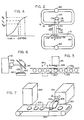
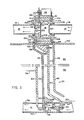
- the laser generating device 10 includes a laser beam generating chamber housing 12 within which an elongated laser beam generating chamber 14 is defined, as depicted in FIGS. 2 and 3, and from which a pulsed laser beam is projected, as indicated at 15. in FIG. 1.
- a transverse gas conduit 16 is formed into a recirculating loop and defines a gas passageway 18, illustrated in FIGS. 2 and 3.
- an elongated gas permeable anode 20 and a gas permeable cathode 22 are elongated mesh screens, perforated strips, honeycomb structure, or some other gas permeable structure about one meter in length and about 2 centimeters in width across the gas flow passageway 18.
- the anode 20 and cathode 22 are constructed of some metal compatible with the gas mixture utilized in the gas flow chamber 18.
- the anode 20 and cathode 22 may both be formed of aluminum, nickel or stainless steel.
- a series of spaced pairs of preionizing electrode pins 24 are located in the laser beam generating chamber 14 and are coupled to a common metal plate 26, forming a wall of the housing 12. _The electrode pins 24 are bent back upon themselves to point upstream and away from the center of the passageway 18.
- the preionizing pins 24 are constructed of stainless steel tantalum, or possibly nickel or rhenium.
- the preionizing pins 24 and the anode 20 and the cathode 22 are interconnected to first apply an ionizing potential between the preionizing electrodes 24 and the cathode 22, and to thereafter produce a spacially uniform laser discharge between the cathode 22 and the anode 20.
- a pulse triggered multichannel bar gap switch is indicated generally at 28 in FIGS. 2 and 3.
- the bar gap switch 28 is connected to the preionizing electrodes 24 and to the anode 20 by a Blumlein pulse forming network, indicated generally at 30.
- the Blumlein pulse forming network 30 is powered by a conventional pulse power source on line 32.
- the power source on line 32 pulses the Blumlein pulse forming network 30 with a pulse charge of from 50 to 6 0 kilovolts in five microseconds or less and at a frequency of at least 100 hertz.
- the pulse source is connected to the bar gap switch 28 by line 34 by a coupling arrangement of predetermined delay which is responsive to the pulses on line 32.
- the bar gap switch 28 creates multichannel sparks only after the voltage applied on line 34 has exceeded the ionizing breakdown voltage of a gaseous medium flowing in a second gas flow passageway 41.
- the Blumlein pulse forming network 30 includes a plurality of parallel electrode plates 42,44 and 46, which are housed within a liquid dielectric chamber 48.
- the liquid dielectric chamber 48 is constructed generally in the form of a rectangular prism with walls 50, a roof 52, and a floor 54 constructed of some dielectric material, such as phenolic resin, plexiglass, alumina or some other dielectric.
- the dielectric chamber 48 contains a liquid dielectric, which may be distilled water or alcohol indicated generally at 56 in FIG. 3.
- liquid dielectric chamber 48 is quite long, as ccntrasted with the vertical electrode dimensions, as illustrated in FIG. 3, and for this reason the vertical center section of the dielectric chamber 48 has been omitted from FIG. 3 to allow clear illustration of the electrodes of the laser or laser generating device 10.
- a gas flow conduit 40 is formed into a recirculating loop as illustrated in FIG. 1, to define the gas flow passageway 41.
- the bar gap switch 28 is located in the passageway 41 just below the floor 54 of the dielectric chamber 48, as illustrated in FIG. 3.
- the gas flew conduit 16 is connected to the laser beam generating chamber housing 1 2 , as illustrated in FIG. 1, and is constructed in a closed loop and includes a fan or gas pump 60 for forcing a mixture of helium, a rare gas and a halogen or gas halide through the first gas passageway 18 and through the laser beam generating chamber 14.
- the rate of gas flow in the passageway 18 is sufficient to clear gas from the vicinity of the anode 20, cathode 22 and preionizing electrodes 24 with each successive pulse on the Blumlein pulse forming network 30.
- the distance between the anode 20 and cathode 22 is two centimeters, and the distance between the cathode 22 and the preionizing electrodes 24 is one centimeter, and if the pulse repetition rate on line 32 is one hundred hertz, the gas volume between the anode 20 and preionizing electrodes 24 must be cleared every one hundredth of a second.
- the gas conduit 40 is likewise arranged in a recirculating loop with gas driven by a pump 62, as illustrated in FIG. 1.
- the electrode plates 42, 44 and 46 of the Blumlein pulse forming network 30, and the trigger line electrode plate 64 extend through the floor 54 of the liquid dielectric chamber 48 into the gas flow conduit 40 as depicted in FIGS. 1 and 3.
- the gas composition flowing through the conduit 40 is typically nitogren, air, or a mixture of sulfur hexafluoride in nitrogen.
- the gas composition in the conduit 16 is a mixture of helium with a rare gas and a'halogen or gas halide. Xenon, argon or krypton may be utilized as the rare gas, while fluorine, chlorine, iodine, bromine or hydrogen chloride may be used as the halogen component. 'A suitable mixture might be helium-94.8 %, xenon-5% and hydrogen chloride-.2%.
- the pressure in the conduit 41 is maintained at from 1 to 5 atmospheres psia.
- Electrodes 42, 44, 46 and 64 in the liquid dielectric chamber housing 48 must be resistive to attack or degradation by the liquid dielectric 56 therein. If that dielectric is water, for example, the electrode plates may be stainless steel or nickel coated aluminum. Alternatively, the plates might be solid nickel.
- the trigger line electrode plate 64 extends into the gas flow passageway 41 formed by the conduit 40 and terminates in'a multiplicity of L-shaped trigger pins 68, which extend upstream at spaced intervals as indicated in FIGS. 1 and 3. Typically one hundred separate trigger electrode pins 68 are arranged in this manner.
- the trigger pins 68 are typically constructed of brass or tungsten, but may also be formed of stainless steel..
- the electrode plates of the Blumlein 30 terminate in a pair of rail electrodes 70 and 72, located in the gas flow passageway 41 in the conduit 40.
- the rail electrode 70 is an electrically conductive elongated bar constructed for example of tungsten, molybdenum, brass or copper.
- the bar electrode 70 has a rounded front edge about one meter in length and is configured to define spaced apertures 74 on the rounded upstream facing surface thereof facing the other rail electrode which is a blade electrode 72.
- the spaced apertures 74 meet corresponding spaced enlarged concavities 76 defined in the reverse or back or downstream side of the bar electrode 70 opposite the blade electrode 72.
- the trigger pin electrodes 68 are embedded in these concavities 76 in spaced relationship therefrom and extend proximate to the apertures 74 as depicted in FIG. 3.
- a plurality of apertures 78 are defined in that portion of the electrode plate 42 which extends into the gas flow passageway 41 to faciliate gas flow therethrough and to prevent turbulence in the gaseous medium in the passageway 41 in the conduit 40.
- the other rail electrode, the blade electrode 72 is a planar or blade-like structure of good conductivity and having a high melting point.
- the blade electrode 72 may be constructed of tungsten, or molybdenum or tantalum.
- the blade electrode 72 may be a replaceable structure and is locked in disposition parallel to the direction of gas flow-and aligned in a plane passing through the apertures 74 in the bar electrode 70 by a locking screw 80 which secures the blade like electrode 72 in an electrically conductive torpedo shaped mounting 82.
- the torpedo shaped mounting. 82 is secured to the extremity of the electrode plate 44 protruding into the gas flow passageway 41 by means of a series of locking screws 84.
- a plurality of apertures 86 are defined in the electrode plate 44 to facilitate gas flow through the passageway 41 and to prevent turbulence therein. This ensures that residual ions will be swept from the vicinity of the rail gap switch 28 after each pulse.
- the electrode plate 42 and at the upper end of the electrode plate 44 in the Blumlein pulse forming network 30 in the dielectric chamber housing 48 there are triangular shaped structures 88 which serve as flux excluders.
- the flux excluders 83 are attached to the electrode plates as indicated by fastening screws 90.
- the purpose of the flux excluders 88 is to maintain the effective spacing between the electrode plates 42 and 44. During operation of the laser generating device 10, the impedance per unit length between the electrode plates 42 and 44 will remain constant unless the spacing therebetween changes.
- the electrode plates Because of the necessity for configuring the electrode plates to conform to the electrodes of the pulse triggered multi-arc channel switch 28, and also to the electrodes in the laser beam generating chamber 14, spacing of the electrode plates must be altered between the'plates 42 and 44 as indicated in FIG. 3. To prevent the inductance in the gap between the electrodes 42 and 44 from increasing, the flux excluders 88 are provided. Without them, an inductance mismatch would exist and the electrical energy would be partially reflected by the impedance discontinuity in the plates 42 and 44. As a result, the efficiency in the transfer of energy from the Blumlein pulse forming network 30 to the preionizing electrodes 24 would suffer.
- the laser beam generating housing 12 is formed with .metallic, conductive walls 26 and 92.
- the electrode plate 42 of the Blumlein pulse forming network 30 is electrically coupled to the plate 26 by a contact interface immediately above the roof 52 of the dielectric chamber housing 48.
- the electrode plate 42 is fastened to the plate 26 by means of metal screws 94.
- the electrode plate 46 of the Blumlein pulse forming network 30 passes through the roof 52 of the dielectric chamber housing 48 and is electrically coupled'to the plate 92 by means of fastening screws 94 in a surface to surface interface of contact.
- a positioning plate 98 is used to locate the laser beam generator chamber housing 12 atop the dielectric chamber housing 48. Above the positioning plate 98 there are a number of insulating spacing rods 102 to which the electrically conductive plates 26 and 92 are fastened by means of screws 104.
- the walls of the laser beam generating chamber -14' are- defined by opposing longitudinally extending electrically insulating channel-shaped structures 106 and 108, which also serve as cathode retainers.
- the channel structures 106 and 108 are typically formed of teflcn or kynar, and are positioned relative to the electrically conductive plates 26 and 92 and sealed by means of O-ring seals 110 as indicated.
- An annular electrically insulating spacing ring 112 is located interiorally of the metal plate 26 downstream from the channel structures 106 and 108 at the laser beam generating chamber 14 and surrounding the preionizing electrodes 24.
- a metal cathode retainer ring 114 is located immediately upstream thereof and is used to electrically couple the cathode 22 through an electrical connecting rod 116 to spaced capacitors 118 through threaded coupling nipples 120 which are threadably engaged with a longitudinal top plate 122 of the laser beam generating chamber housing 12.
- the total capacitance of the capacitors 118 is equal to approximately 5,000 picofarads.
- Upper insulating spacing rods 124 are used to space the upright electrically conductive plates 26 and 92 and are fastened thereto by means of screws 104.
- Flanges 126 of the gas passageway ccnduit 16 are fastened to the metal plates 26 and 92 by means of fastening screws 90 to maintain a gas tight seal about the passageway 18.
- the anode 20 and the preionizing electrodes 24 are coupled together by an inductor 130 which is typically from 0.1 to 1 micrchenry in value.
- the inductor 130 poses a-very small inductive impedance during charging of the Blumlein pulse forming network 30 by the pulse charge on line 32, which occurs over a period of approximately one microsecond.
- the pulse charge on line 32 thereby effectively charges both sides of the Blumlein 30 concurrently by means of the voltage potential which exists on the electrode plate 44 relative to the plates 42 and 46.
- Firing of the . trigger line electrical plate by means of the line 34 results in a fast rising 10 nanosecond pulse.
- the impedance of the inductor 130 is very large so that a considerable voltage differential exists between the electrode plates 42 and 46 at this time.
- resistors 132 couple the preionizing electrodes 24 and the cathode 22.
- the resistors 132 thereby drain any residual static charge left on the cathode 22 from the last previous pulse.
- the value of each of the resistors 132 may be between 100 and 10,000 ohms.
- the value of the resistors 132 and-the value of the capacitors 118 are related in that the RC time constant must be less than the repetition rate. That is, in the embodiment as contemplated, the RC time constant must be less than one milisecond, preferably between a milisecond and a microsecond.
- the laser beam generating chamber. housing 12 has a partially beam transparent window 13 at one end, and a mirror (not visible) at the opposite end.
- the gas flow passageway 18 transversely intersects the beam generating chamber 1 4 , as illustrated in FIGS. 1 and 3.
- the pulsed voltage is applied on line 32 to raise the potential on the electrode plate 44 relative to both of the electrode plates 42 and .46.
- the pulse on line 32 triggers a short, fast rising pulse on line 34. This pulse is less than 100 nanoseconds in duration.
- the inductor 130 exhibits a high impedance at this time and the trigger pin electrodes 68 produce a breakdown in the gas flow in the passageway 41 relative to the rail electrodes 70.
- the voltage at which line 34 is triggered is indicated at V m .
- This voltage is greater than the natural d.c. breakdown potential of. the gap between the rail gap electrodes 70 and.72, indicated at V DC in FIG. 4.
- the trigger voltage V T is less than the voltage V S at which breakdown-will occur between the electrodes 70 and 72 without a triggering pulse. Because the exact voltage V s does not occur with consistent uniformity, the lower.voltage V T , above the natural d.c. breakdown voltage V DC achieves the uniformity in discharge voltage required in the system. As the voltage at which the switch is fired, V T , is moved closer to the self switching voltage V S , the faster the gap will breakdown, but the higher probability of the gap self triggering. Therefore, the optimum trigger voltage V T is somewhere just above the natural breakdown voltage VDC.
- the trigger pins 68 are deeply embedded inside the bar electrode-70, they are not effected by the electric field that occurs in the rail spark gap switch 28. Hence there is little or no erosion of the trigger pin electrodes 68. In contrast, in prior-trigger pin electrode systems - the trigger pin electrodes usually suffer severe ion bombardment and hence severe erosion.
- the trigger pins 68 of the present invention are protected by their configuration and positioning in the concavities 76 in the back of bar electrode 70. While electrons and ultraviolet radiation are able ta pass freely from the trigger pins 68 through the apertures 74 to the blade electrode 72, the trigger pins 68 are shielded from ions during discharge by the protective structure of the bar electrode 70.
- the cathode 22 is-held at the potential of the anode.20 because of the capacitance provided by the capacitors 118
- the capacitors 118 are charged in a period of about 5 nanoseconds. Once the capacitors 118 are charged, the voltage rises at the cathode 22. When it rises above the natural breakdown voltage V DC , then an avalanche of electrons are created in the gas in the laser beam generating chamber 14.
- An energy output of the laser beam 15 in the range of from 2 to 5 joules is produced with each pulse.
- the pulsed laser outputs occur at a frequency of at least 100 hertz, and more typically one kilohertz.
- FIGS. 5, 6 and 7. The application of the laser beam generating device 10 to the manufacture of solar voltaic cells is illustrated in FIGS. 5, 6 and 7.
- conveyor belt 120 is operated in stepped movement at specific intervals to transport disk-shaped wafers-122 of silicon past an' annealing station at which the laser generating device 10 scans the wafers 122 with the laser beam 15.
- the wafers 122 may be typically about 8 centimeters in diameter and of variable thickness.
- the wafers 122 Prior to arriving at the annealing station at which they are treated by the laser beam 15 of the laser generating device 10, the wafers 122 are first implanted with a suitable dopant, typically boron, phosphorus or arsenic.
- the dopant may be deposited by one of several conventional techniques. Typical doping techniques are described and referred to in U.S. Patent 4,147,563.
- FIGS. 5 and 7 illustrate a conventional dopant implantation unit 124 which is used to deposit boron or some other dopant material on the wafers 122 as the conveyor belt 120 moves from left to right as indicated.
- the silicon wafers 122 move into alignment with the laser beam 15.
- the laser beam 15 is projected through a cylindrical lens 128 which reshapes the beam from the cross section of the window 13 in the laser generating device 48 to a swath 130 which is approximately four milimeters in thickness by about 8 centimeters in length aligned with the direction of movement of the conveyor belt 120, as illustrated in FIG. 5.
- the laser generating device 10 is typically located to the side of the conveyor belt 120 and transmits the beam 15 through the cylindrical lens 128 as the reshaped beam 130 laterally to a tilted mirror 132 which reflects the beam'130 downward onto the wafers 122 as they pass beneath on the conveyor belt 120.
- the mirror 132 may be tilted alternatively to scan the rectangular swath 130 across the entire wafer 122 located therebeneath.
- the beam 15 delivers energy at 1 to 2 joules per square centimeter at a laser repetition rate of 100 hertz. Two square centimeters of the wafer are therefore treated with each laser pulse so that it requires 50 pulses from the laser generating device 10 to anneal an entire wafer 122. This requires approximately 1/2 second at a laser repetition rate of 100 pulses per second. Consequently, at this repetition rate approximately 2 wafers can be annealed each second, A throughput of approximately 7,000 wafers per hour is therefore easily achieved. This throughput can be increased by a magnitude of 10 by merely operating the laser generating device 10 at a repetition rate of 1 kilohertz, a rate easily achieved with the device of the invention.
- wafers 122 formed of monocrystalline silicon may be annealed in this fashion.
- polycrystalline silicon wafers 122 can each beregrown into monocrystalline structure by annealing with the laser generating device 10.
- amorphous silicon can be deposited as silicon tetrachloride through vapor deposition on saphire or graphite. With the laser generating device 10 of the invention, monocrystalline silicon can be grown upon a disk-shaped saphire or graphite base through the annealing process described herein.
- the critical features in treating the silicon wafers 122 to create a P-N junction for use as solar voltaic cells include annealing the silicon with a pulse laser beam having a wavelength predominantly in the ultraviolet region, a beam energy of at least 2 joules per pulse, a pulse repetition rate of at least about 100 pulses per second and a uniformity of beam pulse output that varies by no more than 5 percent -across the area of beam output.
- dopant implantation .and annealing according to the invention using the laser beam generating device 10 are carried out at atmospheric pressure in air.
- the laser beam energy per pulse is from about 2 to about 5 joules and the average power achieved is several hundred watts, typically from about 200 to 500 watts. Laser uniformity of better than five percent may be achieved with the laser beam generating device 10 of the invention, and a uniformity of from 2 to 5 percent is typical.
Abstract
A high power excimer laser (10), suitable for annealing semiconductor wafers, emits a pulsed output at a high repetition rate in the ultraviolet wavelength region having a uniform power output across the laser beam (130).
A uniform discharge is caused beween anode (20) and cathode (22) in a first transverse gas flow passageway (18) automatically following a pulse applied to the preionisation electrodes (24). The pulses are formed by a multichannel bar gap switch (28) in a second gas flow passageway (41), which is connected to the first passageway (18) by a Blumlein network (30).
Description
- The present invention relates to an excimer laser generating device for producing a pulsed output at a high repetition rate and with uniform power output across the beam aperture, for use in annealing solar photo-voltaic cells.
- In the manufacture of solar photo-voltaic cells, a semiconductor junction must be produced which will respond to incident solar radiation by producing a flow cf electrons, and a counterflow of "holes". The element silicon, when suitably doped to form a P-N junction, responds in this fashion. Typical dopant materials include boron, phosphorous and arsenic. The electrical conversion efficiency of conventional solar voltaic cells is from about 10 to 16 percent. That is, 10 to 16 percent of incident radiant solar energy is converted to electrical energy using doped silicon wafers as solar voltaic cells. Other photosensitive semiconductor substrate materials may be substituted for silicon, for example gallium arsenide, germanium, gallium phosphide, indium phosphide cadmium telluride, aluminum antimonide, cadmium sulphide, copper oxide, and others.
- The principal problem that arises in the manufacture . of solar voltaic cells according to the present state of the art is that in order to implant the dopant material, the underlying silicon crystalline structure is damaged during the ion implantation process. That is, the implantation process removes atoms from an orderly crystalline latticework at the implantation site, and creates partial and disoriented latticework regions. This damage is repaired, according to the current state of the art, by extended heating of the doped silicon wafers following implantation of the dopeant material for several hours at temperatures typically above 200° C. Furthermore, with the present state of the technology, only monocrystalline silicon is useful in the manufacture of solar voltaic cells, since a single crystalline lattice work is necessary in order to achieve a directed current. flow, and hence a current which can be applied to external circuitry. The production of monocrystalline silicon is far more costly than polycrystalline or amorphous-silicon, and much less readily available. As a consequence, the high cost of manufacture has thus far precluded the use of solar voltaic cells as a source of electrical power for any but the most exotic applications. To date, the use of solar voltaic cells as a source of electrical energy has been commercially significant only in supplying power to vehicles and instruments used beyond the earth's atmosphere, - and instruments which must necessarily be used in remote, unattended locations.
- There are two general type of conventional dopant implantation techniques used in the manufacture of solar voltaic cells. In the ion implantation technique the dopant is a high energy ion beam of a number of kilovolts. The impurity ions of arsenic, phosphorous or boron are rammed into the lattice structure of the silicon wafer with this high energy beam. This damages the crystal lattice structure of the monocrystalline silicon wafer, which necessitates subsequent annealing. In the other commercially signficiant technique of dopant implantation, the dopant material is applied to the surface of a monocrystalline silicon wafer and thereafter thermally diffuses into the wafer. The thermal diffusion process complicates the manufacture of the cells, and adds to the manufacturing expense the same as high temperature thermal annealing.
- Various attempts have been made to utilize laser beams for the purpose of annealing doped silicon wafers following implantation of the dopant material. This annealing has been attempted both to reform monocrystalline silicon structure, and also to transform amorphous or polycrystalline silicon into a monocrystalline structure following dopant ion implantation. For example, U.S. Patent No. 4,151,008 describes a pulsed laser annealing process which utilizes a necdynium-yag iaser bean to effectuate annealing. Such a laser produces a beam which does not directly produce the ultraviolet wavelength so readily absorbed by silicon. Also, the pulse repetition rate achieved with such a laser is relatively low (0-20 pulses per second) limiting the average laser output power, and hence limiting the procesing capability of this type of system. Because of the low repetition rate and infrared wavelength of the yag laser, the annealing process using such a device requires an excessively large input power applied over a prolonged period of time. To achieve an ultraviolet output, an ultraviolet-flash lamp was employed in place of the laser. However, the light output produced by the ultraviolet flash lamp is quite difficult to focus in order to achieve the required energy density to effectuate semiconductor.annealing. In such an ultraviolet flash lamp system, the energy per pulse achieved in the beam and beam uniformity are both poor. While interesting as a laboratory tool, such a system is not feasible for use in the mass commercial manufacture of solar voltaic cells.
- U.S. Patent 4,154,625-also deals with the use of a laser. in annealing semiconductor devices, and the fabrication of polycrystalline solar cells in particular. This patent suggests lasers in the optical range, but a ruby laser was utilized. The wavelength of a ruby laser is primarily in the red visible and- infrared regions, not the ultraviolet where silicon- absorbs energy well. Lasers such as this which project beams in the infrared and visible range are capable of high peak power, but their beam uniformity has historically been poor. The energy level obtained with the ruby laser is quite large, but with the poor beam uniformity achieved large localized temperature variations in the silicon exist. The silicon therefore is melted and reforms to a polycrystalline or monocrystalline structure at some implantation sites while the energy applied is inadequate to induce epitaxial regrowth at adjacent sites. U.S. Patent 4,147,563 utilizes a similar ruby laser t6 implant impurities in silicon in the manufacture of solar cells, rather than to anneal the silicon following implantation.
- U.S. Patent 4,059,461 suggests the use of a'continuous wave Nd:YAG laser for purposes of annealing silicon in the fabrication of solar voltaic cells. The laser suggested operates at only 6 or 7 watts of power, however, although lasers of larger power output, such as CO or C02 having a power output of 100 watts are contemplated. However, such lasers operate primarily in the infrared region. Because of the lower absorption of silicon, in this region, a higher average power is necessary to achieve annealing. This excessive power produces excessive heating of the entire silicon wafer, which can distort or damage the entire wafer. Laser scanning is applied to polycrystalline semiconductor material in annealing. However, the laser systems employed according to this patent do not provide sufficient power and do not obtain an acceptable throughput rate. A complete heating and cooling cycle of doped silicon took approximately 10 minutes. In continuous wave scanning the beam must be focused to a very tiny point. This necessitates intricate mechanical apparatus to control a scan pattern. Also, in continuous wave annealing epitaxial regrowth is induced in the solid phase, not the liquid phase as in pulsed annealing processes. Consequently, the quality of repair to the damaged lattice sites is not as good in continuous wave annealing as contrasted with pulsed annealing. Accordingly, such a device could not feasibly be scaled for the commercial manufacture of solar voltaic cells.
- According to the present invention there is provided an excimer gas laser including means defining an elongated laser beam generating chamber and a first transverse gas flow passageway,
anode means, cathode means and preionizing electrode means located in said laser beam generating chamber and interconnected to first apply an ionizing potential between said preionizing electrode means and said cathode means, and to thereafter produce a spatially uniform laser discharge between said cathode means and said anode means,
pulse triggered multichannel bar gap switch means connected to said preionizing electrode means and said anode means and located in a second gas flow passageway, and
pulsed voltage means coupled to said pulse triggered multichannel bar gap switch means to repetitively apply brief, fast rising pulses thereto to create multichannel sparks therein only after the voltage applied has exceeded the ionizing breakdown voltage of a gaseous medium flowing in said second gas flow passageway. - The pulsed excimer gas laser of the invention overcomes the deficiencies present in prior lasers used for the annealing of silicon or other useful semiconductor materials in the manufacture of solar voltaic cells. The laser of the present inventicn has a high energy output per pulse, typically from 2 to 5 joules per pulse. Moreover, the laser of the present invention operates at a high pulse repetition rate. Repetitions in the range of at least a kilohertz are readily achieved. This repetition rate, coupled with the high energy output per pulse achieves a high average power output during operation of the device. The laser of the invention produces several hundred watts of average power, typically from 200 to 500 watts, during operation.
- Furthermore, the pulsed excimer laser of the present invention achieves a high degree of uniformity of power output across the beam aperture, and at a wavelength in the ultraviolet range. The amplitude of power output across the beam aperture is extremely uniform, and varies by no more than from 2 percent to 5 percent.
- All of the foregoing features of the excimer laser of the invention render the device particularly suitable for laser annealing of doped silicon in the commercial manufacture of solar voltaic cells. The ultraviolet wavelength produced by the laser of the invention is readily absorbed .by silicon and other semiconductor materials used in solar voltaic cells, and the beam uniformity achieved prevents any major'discontinuities in crystal regrowth from occuring during the annealing process.
- The laser of the invention is able to stimulate liquid phase epitaxial regrowth in monocrystalline silicon to quickly repair damage that occurs during the implanation process. It is well known that monocrystalline silicon, even with a damaged crystalline latticework, can be regrown free of crystalline defects when suitably annealed. The pulsed excimer laser of the present invention achieves this regrowth with greater uniformity and far more quickly than lasers heretofore employed for annealing monocrystalline oralarge grain polycrystalline silicon in the manufacture of solar voltaic cells.
- Moreover, the laser of the invention can be utilized to reform polycrystalline or amorphous siliccn into a monocrystalline structure in the manufacture of solar voltaic cells. With the uniform application of energy to a polycrystalline silicon structure, the small crystals of that structure can be regrown and reformed into a large, monocrystalline structure. Furthermore, even amorphous silicon can be laser annealed with the laser of the present invention to produce a monocrystalline or a large grain polycrystalline silicon structure. For example, SiCl4 can be vapor deposited .onto saphire or graphite. The laser bean of the excimer laser of the present invention, when applied to this structure, reforms the silicon present into a single, monocrystalline structure grown from the saphire or graphite base.
- A self-sustained volume discharge initiated by a homogeneous electron avalanche is a convenient method of gas laser excitation. The method involves the sudden application of a strong electric field considerably in excess of the breakdown threshold across the laser gas. This causes the initially low level of ionization within the discharge gap to grow exponentially via the electron avalanche process until the plasma impedance becomes limited by the output impedance of the driving electrical circuit. The driving circuit impedance, in turn, must be so chosen that electrical excitation of the laser gas mixture can progress at the desired rate during the main part of the current pulse. This method of excitation has been successfully employee in many transversely excited atmospheric-pressure (TEA) lasers such as CO2, N2, HF, and more recently, in the rare. gas halide and metal halide excimers such as KrF, XeF, XeCl, ArF, HgCl, HgBr, HgI, etc. These lasers have proven to be a powerful source of infrared, visible, and ultraviolet coherent radiation due to the high density, and hence, high energy handling capacity of the high pressure gas.
- The high pressure gas lasers based on the pulsed discharge method of excitation just described are usually referred to as "fast discharge lasers." This nomenclature is used since it has been found from experience that the high voltage electrical pulse creating the electron multiplication in the laser gas must have a very fast rise tine and also a relatively short duration (of the order of 10-8 sec) in order to avoid the formation of filamentary arcs within the discharge volume. Efficient laser pumping in the presence of severe arcing is, of course, impossible due to the inadequate excitation rates in regions of low current density and the too rapid thermal equilibration rate (which tends to destroy population inversion) in regions of very high current density. In addition, the resultant non-uniform distributions of refractive index within the inhomogeneously excited medium also make formation of high optical quality laser beams difficuLt. Another problem associated with the onset of severe arcing in discharge pumped lasers is the very low plasma resistivity within the concentrated arcs. The sudden decrease in plasma resistivity with rapidly increasing local current densities may cause the total load resistance across the discharge gap to collapse momentarily to values far below that of the driving circuit output impedance. When this occurs the discharge will either self terminate or go into an unstable oscillatory arc discharge mode, depending on the characteristics of the driving circuit and on the extent of the impedance mismatch. Such premature termination or interruption of the discharge, together with ineffective excitation due to non-uniform current distributicn in the presence of severe arcing, tends to limit the total energy cutput of the laser. This arcing problem has been found to be especially troublesome in the generation of rare gas halide and metal halide lasers where efficient formation of the excimers generally requires a high uniform rate of electron impact excitation. The very presence of the electrophilic halogen molecules and excited metastable rare gas atoms tends to make the electron multiplication and disappearance rates very sensitive functions of the local electrtic field strength and current density. Accordingly, with the exception of some very recent work the effective discharge volume, pulse duration, and maximum laser energy output have all been very low (typically of the order of 0.1 liter, 10 nanoseconds, and 0.1 joules per pulse, respectively).
- The foregoing difficulties of high pressure discharge undoubtedly related to the absence of strong electronic and ionic diffusion effects responsible for homogenization and stabilization of low-pressure "glow discharges." To bypass these difficulties, high energy electron beans have .been successfully utilized both as a direct pumping source and as a stabilizing ionization source for homogeneous excitation of high pressure gas lasers over extended volumes. In many practical applications (for example, applications requiring high pulse repetition rates), however, the avalanche/self-sustained discharge method has the advantage of relative simplicity when compared with either the electron-beam-pumped or the electron-beam-sustained discharge method. The simplicity of the avalanche/self-sustained discharge method is mainly a result of the lower voltage requirement and the absence of fragile foil windows needed for transmission of the high energy electron beams at high current densities.
- The physical structure of the laser beam generating device of the present invention is quite different from lasers of prior design. This is due, in large part, to the unique principal by means of which homogeneity in the gas plasma in the laser generating chamber is achieved. In many conventional avalanche discharge lasers, a spark gap switch is employed to cyclically bring the cathode and anode in a laser beam generating chamber to a sufficient differential voltage to apply power to a gas contained therein. Power is applied by means of an electric discharge into the gas- between the anode and cathode to raise the energy level of electrons in electron shells in the gas to a higher state. If this energy is sufficient to achieve a laser threshold, some of the electrical energy will be converted to electromagnetic energy as laser radiaticn.
- As delineated by Levatter and Lin, "Criteria for Maintaining a Uniform Formative Phase During a High Pressure Avalanche Discharge", Gaseous Electronics Conference, Buffalo, NY, 1979, there are several criteria that must be met in order to achieve a uniform large.volume avalanche discharge without the formation of streamers. These criteria are: (1) the electric field between-the discharge electrodes must be uniform (2) the discharge volume must -be preconditioned by creating a spatially uniform level of electron density (preionization) of between 10 to 108 centimeters -3, the exact value depending upon the nature of the gas mixture and gas pressure; and, (3) the rate of change of the voltage (dV/dt) applied to the discharge electrodes must be at least 1012 volts per second.
- To date there have been only two transverse electric (TE) discharge lasers that have fully met the above criteria. The first is the ultraviolet preionized H2O Blumlein laser described in an article by Levatter and Bradford, "Water Blumlein Driven Fast Electric Discharge KrF Laser, " Applied Physic's Ltrs., Vol. 33, pages 742-744, 1978, and the second is the x-ray preionized double transmission line laser of Lin and Levatter "X-ray Preionization for Electric Discharge Lasers" Applied Physics Letters Vol. 34, pages 505-508, 1979.
- The water dielectric Blumlein transmission line switch laser is operated by a self-triggered rail spark gap similar to that described by J.C. Martin in "Multichannel Gaps"
Switching Note Number 10, SSWA/JCM/703/27, Atcmic Weapons Research Establishment, Aldermaston, England. The rail gap in this laser is pulse charged to a voltage above its natural d.c. voltage breakdown VDC. When the gap is sufficiently overvoltaged, the gap breaks down in numerous parallel arc channels. The pulsed voltage can exceed VDC for a short duration because initially there are not electrons within the gap to start the avalanche, and because it takes a finite time for the initial spark channel to grow into an arc. Although this type of switch does produce the required dV/dt, the statistical nature of the breakdown process in-an unpreionized gap is such that the amplitude and time jitter of the breakdown are very large. This makes this particular water dielectric Blumlein driven laser system unsuitable for the manufacture of solar voltaic cells. The x-ray preionizated electric discharge laser by Lin and Levatter uses a similar switch, and has the same limitation. - In order to achieve a homogeneous volume avalanche discharge suitable for laser excitation, it is necessary to uniformly preionize the discharge volume. In the water - dielectric Blumlein driven discharge laser, ultraviolet radiation from multiple sparks generated inside the laser cavity was used to produce the required preionization. In the x-ray preionized electric discharge laser, x-rays generated by an external electron beam were used for the same purpose. In both of these systems the preionization source was powered by a separate pulse forming network and energy storage bank. making the entire system less efficient and requiring critical time delay circuitry to control the timing between preionization and the main discharge.
- The gas laser system of the present invention is a high repetition rate, uniform volume, transverse electric discharge laser with pulse triggered, multi-arc channel switching. This laser system creates a large volume homogeneous avalanche electric discharge in almost any gas mixture with a very high ratio of electric field to gas density. The laser system of the invention incorporates a folded Liquid Blumlein pulse forming network as the electrical drive circuit along with a unique fast. parallel arc channel ultraviolet discharge preionization source that does not require any additional drive circuitry or energy supply.
- The laser pulse forming network is switched by a bar gap of unique construction that is capable of very large rates of change of voltage and current. The rate of current change, is greater than 1013 amps per second and the voltage rate of change is greater than 1013 volts per second. The pulse triggered device allows the switch to operate with several hundred arc channels per meter of gap width, yet is not susceptible to trigger erosion or to transient electrical coupling which can limit the useful lifetime of ordinary triggered spark gaps. The laser cavity and multi-arc channel spark gap of the invention are also fully compatible with fast, high volume rate gas flow allowing the entire system to operate at high repetition rates and hence high average power for long periods of time without maintenance.
- The laser system of the present invention overcomes the problem of time and amplitude jitter characteristic of the water dielectric Blumlien driven and x-ray preionization lasers by injecting a burst of ultraviolet radiation and electrons directly into the discharge switch at selected points. This causes the switch to breakdown in a large number of separate arc channels simultaneously. Unlike a conventional trigatron switch in which the applied voltage never exceeds the natural d.c. breakdown potential of the gap, the voltage pulse in the spark gap of the present invention is applied in a short pulse of less than one microsecond to a potential greater than the d.c. breakdown voltage level VDC. If the gap is not triggered, it will break down at some point above the d.c. voltage breakdown level. This higher, self-triggering level will vary, however. To trigger the switch of the present invention, electrons are injected directly into the rail gap by means of a spark created between the trigger pin electrodes and one of the rail gap electrodes after the voltage has exceeded the d.c. breakdown voltage. As the voltage at which trigger operation is fixed is moved closer to the self-breakdown voltage, the faster the gap will break down, but the higher will be the probability of the gap self-triggering thus creating time jitter.in the overall breakdown process. The optimum trigger point is therefore somewhat just above the d.c. voltage breakdown level VDC so that a consistent voltage breakdown level is achieved.
- Preionization in the laser system of the present invention is automatic, and no active time delay circuitry between preionization and the main discharge is required. Accordingly, no time delay circuitry between the application of power to the preionizing electrodes and the application of power to the laser cathode is necessary. Preionization is obtained from multiple, parallel ultraviolet sparks behind a gas permeable cathode.
- The Levatter and Bradford water dielectric Blumlien driven dicharge laser employed an array of 120 preionization pin electrodes that arced to a blade mounted between a screen cathode and its support ring. However, a delay circuit was necessary to synchronize the application of preionization voltage to the preionizing pins and the application of the discharge voltage pulse to the cathode. In another system, preionization was obtained from multiple series spark gaps known as spark boards, positioned behind a cathode. Such a device is described in H.J. Sequin et al, IEEE Journal of Quantum Electronics QE-11, pages 774 et seq., 1975. This device produced sparks that occurred sequentially, thus causing a time delay and uniformity problems in the .main laser discharge. This device also required a separate pulse forming network for the preionization charge and for the main discharge.
- According to the present invention, multiple parallel sparks are produced that operate in series with the main laser pulse forming network. When the bar gap of the laser has switched, a fast rising (less than 10 nanosecond ) high voltage pulse arrives at the preionization electrodes, thus causing the preionizing pin electrodes to break down to the laser cathode in the form of multiple parallel sparks. Because the voltage rise time is very fast, all of these sparks happen simultaneously and with a delay determined solely by the value of the capacitance connected between the anode and cathode which serves to hold the cathode to ground potential for the first few nanoseconds of operation. Atter this fixed and automatic delay, a high voltage fast rising voltage differential develops across the anode and cathode of the laser gap resulting in a uniform volume discharge in the laser generating chamber. Because the parallel ultraviolet preionizing sparks are in series with the laser pulse forming network, no additional energy is required to drive them, and incorrect timing of the preionizing discharges and main discharge cannot occur.
- Because of the unique trigger electrode configuration and interconnection of the electrodes of the present invention, a pulsed laser output is achieved which has a beam uniformity and pulse repetition rate heretofore unobtainable with prior laser systems. Moreover, the.power cutput achieved-in the excimer laser of the invention is much higher in the ultraviolet region than has previously been obtained. These features make the laser of the present invention uniquely suited for laser annealing of solar voltaic cells, and for the mass, commercial manufacture of such cells.
- . The invention may be-described with greater clarity and-particularly by reference to the accompanying drawings in which:-
- FIG. 1 is a perspective view of the laser of the invention.
- FIG. 2 is a schematic diagram of the. construction of the laser of the invention.
- FIG. 3 is a sectional view of a portion of the laser generating device illustrating the electrode configuration and arrangement.
- FIG. 4 is a graph illustrating the application of pulse charging voltage in the laser of the invention.
- FIG. 5 is a plan view diagramatically illustrating the manufacture of solar voltaic cells according to the invention.
- FIG. 6 is an elevational view diagramatically illustrating the manufacture of solar voltaic cells according to the invention.
- FIG. 7 is a perspective view diagramatically illustrating the manufacture of solar voltaic cells according to the invention.
- An
excimer gas laser 10 constructed according to the present invention is illustrated in perspective in FIG. 1. Thelaser generating device 10 includes a laser beam generatingchamber housing 12 within which an elongated laserbeam generating chamber 14 is defined, as depicted in FIGS. 2 and 3, and from which a pulsed laser beam is projected, as indicated at 15. in FIG. 1. Atransverse gas conduit 16 is formed into a recirculating loop and defines agas passageway 18, illustrated in FIGS. 2 and 3. Within the laserbeam generating chamber 14 there is an elongated gaspermeable anode 20 and a gaspermeable cathode 22, both of which are elongated mesh screens, perforated strips, honeycomb structure, or some other gas permeable structure about one meter in length and about 2 centimeters in width across thegas flow passageway 18..Both theanode 20 andcathode 22 are constructed of some metal compatible with the gas mixture utilized in thegas flow chamber 18. For example, theanode 20 andcathode 22 may both be formed of aluminum, nickel or stainless steel. - A series of spaced pairs of preionizing electrode pins 24 are located in the laser
beam generating chamber 14 and are coupled to acommon metal plate 26, forming a wall of thehousing 12. _The electrode pins 24 are bent back upon themselves to point upstream and away from the center of thepassageway 18. The preionizing pins 24 are constructed of stainless steel tantalum, or possibly nickel or rhenium. - The preionizing pins 24 and the
anode 20 and thecathode 22 are interconnected to first apply an ionizing potential between thepreionizing electrodes 24 and thecathode 22, and to thereafter produce a spacially uniform laser discharge between thecathode 22 and theanode 20. - A pulse triggered multichannel bar gap switch is indicated generally at 28 in FIGS. 2 and 3. The
bar gap switch 28 is connected to thepreionizing electrodes 24 and to theanode 20 by a Blumlein pulse forming network, indicated generally at 30. The Blumleinpulse forming network 30 is powered by a conventional pulse power source online 32. The power source online 32 pulses the Blumleinpulse forming network 30 with a pulse charge of from 50 to 60 kilovolts in five microseconds or less and at a frequency of at least 100 hertz. The pulse source is connected to thebar gap switch 28 byline 34 by a coupling arrangement of predetermined delay which is responsive to the pulses online 32. Thebar gap switch 28 creates multichannel sparks only after the voltage applied online 34 has exceeded the ionizing breakdown voltage of a gaseous medium flowing in a secondgas flow passageway 41. The Blumleinpulse forming network 30 includes a plurality ofparallel electrode plates dielectric chamber 48. The liquiddielectric chamber 48 is constructed generally in the form of a rectangular prism withwalls 50, aroof 52, and afloor 54 constructed of some dielectric material, such as phenolic resin, plexiglass, alumina or some other dielectric. Thedielectric chamber 48 contains a liquid dielectric, which may be distilled water or alcohol indicated generally at 56 in FIG. 3. It is to be understood that the liquiddielectric chamber 48 is quite long, as ccntrasted with the vertical electrode dimensions, as illustrated in FIG. 3, and for this reason the vertical center section of thedielectric chamber 48 has been omitted from FIG. 3 to allow clear illustration of the electrodes of the laser orlaser generating device 10. - A
gas flow conduit 40 is formed into a recirculating loop as illustrated in FIG. 1, to define thegas flow passageway 41. Thebar gap switch 28 is located in thepassageway 41 just below thefloor 54 of thedielectric chamber 48, as illustrated in FIG. 3. - The gas flew
conduit 16 is connected to the laser beam generating chamber housing 12, as illustrated in FIG. 1, and is constructed in a closed loop and includes a fan orgas pump 60 for forcing a mixture of helium, a rare gas and a halogen or gas halide through thefirst gas passageway 18 and through the laserbeam generating chamber 14. The rate of gas flow in thepassageway 18 is sufficient to clear gas from the vicinity of theanode 20,cathode 22 andpreionizing electrodes 24 with each successive pulse on the Blumleinpulse forming network 30. If the distance between theanode 20 andcathode 22 is two centimeters, and the distance between thecathode 22 and thepreionizing electrodes 24 is one centimeter, and if the pulse repetition rate online 32 is one hundred hertz, the gas volume between theanode 20 andpreionizing electrodes 24 must be cleared every one hundredth of a second. - The
gas conduit 40 is likewise arranged in a recirculating loop with gas driven by apump 62, as illustrated in FIG. 1. Theelectrode plates pulse forming network 30, and the triggerline electrode plate 64 extend through thefloor 54 of the liquiddielectric chamber 48 into thegas flow conduit 40 as depicted in FIGS. 1 and 3. - The gas composition flowing through the
conduit 40 is typically nitogren, air, or a mixture of sulfur hexafluoride in nitrogen. The gas composition in theconduit 16, on the other hand, is a mixture of helium with a rare gas and a'halogen or gas halide. Xenon, argon or krypton may be utilized as the rare gas, while fluorine, chlorine, iodine, bromine or hydrogen chloride may be used as the halogen component. 'A suitable mixture might be helium-94.8 %, xenon-5% and hydrogen chloride-.2%. The pressure in theconduit 41 is maintained at from 1 to 5 atmospheres psia. - All of the
electrode plates dielectric chamber housing 48 must be resistive to attack or degradation by theliquid dielectric 56 therein. If that dielectric is water, for example, the electrode plates may be stainless steel or nickel coated aluminum. Alternatively, the plates might be solid nickel. - The trigger
line electrode plate 64 extends into thegas flow passageway 41 formed by theconduit 40 and terminates in'a multiplicity of L-shaped trigger pins 68, which extend upstream at spaced intervals as indicated in FIGS. 1 and 3. Typically one hundred separate trigger electrode pins 68 are arranged in this manner. The trigger pins 68 are typically constructed of brass or tungsten, but may also be formed of stainless steel.. - The electrode plates of the
Blumlein 30 terminate in a pair ofrail electrodes gas flow passageway 41 in theconduit 40. Therail electrode 70 is an electrically conductive elongated bar constructed for example of tungsten, molybdenum, brass or copper. Thebar electrode 70 has a rounded front edge about one meter in length and is configured to define spacedapertures 74 on the rounded upstream facing surface thereof facing the other rail electrode which is ablade electrode 72. The spacedapertures 74 meet corresponding spaced enlarged concavities 76 defined in the reverse or back or downstream side of thebar electrode 70 opposite theblade electrode 72. Thetrigger pin electrodes 68 are embedded in these concavities 76 in spaced relationship therefrom and extend proximate to theapertures 74 as depicted in FIG. 3. - A plurality of apertures 78 are defined in that portion of the
electrode plate 42 which extends into thegas flow passageway 41 to faciliate gas flow therethrough and to prevent turbulence in the gaseous medium in thepassageway 41 in theconduit 40. - The other rail electrode, the
blade electrode 72 is a planar or blade-like structure of good conductivity and having a high melting point. Theblade electrode 72 may be constructed of tungsten, or molybdenum or tantalum. Theblade electrode 72 may be a replaceable structure and is locked in disposition parallel to the direction of gas flow-and aligned in a plane passing through theapertures 74 in thebar electrode 70 by a lockingscrew 80 which secures the blade likeelectrode 72 in an electrically conductive torpedo shaped mounting 82. The torpedo shaped mounting. 82, in turn, is secured to the extremity of theelectrode plate 44 protruding into thegas flow passageway 41 by means of a series of locking screws 84. A plurality ofapertures 86 are defined in theelectrode plate 44 to facilitate gas flow through thepassageway 41 and to prevent turbulence therein. This ensures that residual ions will be swept from the vicinity of therail gap switch 28 after each pulse. - At the lower end of the
electrode plate 42 and at the upper end of theelectrode plate 44 in the Blumleinpulse forming network 30 in thedielectric chamber housing 48 there are triangular shapedstructures 88 which serve as flux excluders. The flux excluders 83 are attached to the electrode plates as indicated by fastening screws 90. The purpose of theflux excluders 88 is to maintain the effective spacing between theelectrode plates laser generating device 10, the impedance per unit length between theelectrode plates multi-arc channel switch 28, and also to the electrodes in the laserbeam generating chamber 14, spacing of the electrode plates must be altered betweenthe'plates electrodes flux excluders 88 are provided. Without them, an inductance mismatch would exist and the electrical energy would be partially reflected by the impedance discontinuity in theplates pulse forming network 30 to thepreionizing electrodes 24 would suffer. - The laser
beam generating housing 12 is formed with .metallic,conductive walls electrode plate 42 of the Blumleinpulse forming network 30 is electrically coupled to theplate 26 by a contact interface immediately above theroof 52 of thedielectric chamber housing 48. Theelectrode plate 42 is fastened to theplate 26 by means of metal screws 94. Similarly, theelectrode plate 46 of the Blumleinpulse forming network 30 passes through theroof 52 of thedielectric chamber housing 48 and is electrically coupled'to theplate 92 by means of fastening screws 94 in a surface to surface interface of contact. - As illustrated in FIG. 3, a
positioning plate 98 is used to locate the laser beamgenerator chamber housing 12 atop thedielectric chamber housing 48. Above thepositioning plate 98 there are a number of insulatingspacing rods 102 to which the electricallyconductive plates screws 104. The walls of the laser beam generating chamber -14' are- defined by opposing longitudinally extending electrically insulating channel-shapedstructures channel structures conductive plates spacing ring 112 is located interiorally of themetal plate 26 downstream from thechannel structures beam generating chamber 14 and surrounding thepreionizing electrodes 24. A metalcathode retainer ring 114 is located immediately upstream thereof and is used to electrically couple thecathode 22 through an electrical connecting rod 116 to spacedcapacitors 118 through threadedcoupling nipples 120 which are threadably engaged with a longitudinaltop plate 122 of the laser beam generatingchamber housing 12. The total capacitance of thecapacitors 118 is equal to approximately 5,000 picofarads. Upper insulatingspacing rods 124 are used to space the upright electricallyconductive plates screws 104.Flanges 126 of thegas passageway ccnduit 16 are fastened to themetal plates passageway 18. - As illustrated in FIG. 2, the
anode 20 and thepreionizing electrodes 24 are coupled together by aninductor 130 which is typically from 0.1 to 1 micrchenry in value. Theinductor 130 poses a-very small inductive impedance during charging of the Blumleinpulse forming network 30 by the pulse charge online 32, which occurs over a period of approximately one microsecond. The pulse charge online 32 thereby effectively charges both sides of theBlumlein 30 concurrently by means of the voltage potential which exists on theelectrode plate 44 relative to theplates line 34 results in a fast rising 10 nanosecond pulse. With a pulse of this nature, the impedance of theinductor 130 is very large so that a considerable voltage differential exists between theelectrode plates - Also as illustrated in FIG. 2,
resistors 132 couple thepreionizing electrodes 24 and thecathode 22. Theresistors 132 thereby drain any residual static charge left on thecathode 22 from the last previous pulse. The value of each of theresistors 132 may be between 100 and 10,000 ohms. The value of theresistors 132 and-the value of thecapacitors 118 are related in that the RC time constant must be less than the repetition rate. That is, in the embodiment as contemplated, the RC time constant must be less than one milisecond, preferably between a milisecond and a microsecond. - The laser beam generating chamber.
housing 12 has a partially beamtransparent window 13 at one end, and a mirror (not visible) at the opposite end. Thegas flow passageway 18 transversely intersects the beam generating chamber 14, as illustrated in FIGS. 1 and 3. - In the sequence of events during repetitive pulsing of the Blumlein
pulse forming network 30, the pulsed voltage is applied online 32 to raise the potential on theelectrode plate 44 relative to both of theelectrode plates 42 and .46. Through the coupling arrangement previously described, the pulse online 32 triggers a short, fast rising pulse online 34. This pulse is less than 100 nanoseconds in duration. Theinductor 130 exhibits a high impedance at this time and thetrigger pin electrodes 68 produce a breakdown in the gas flow in thepassageway 41 relative to therail electrodes 70. - With reference to FIG. 4, the voltage at which
line 34 is triggered is indicated at Vm. This voltage is greater than the natural d.c. breakdown potential of. the gap between therail gap electrodes 70 and.72, indicated at VDC in FIG. 4. However, the trigger voltage VT is less than the voltage VS at which breakdown-will occur between theelectrodes - Since the trigger pins 68 are deeply embedded inside the bar electrode-70, they are not effected by the electric field that occurs in the rail
spark gap switch 28. Hence there is little or no erosion of thetrigger pin electrodes 68. In contrast, in prior-trigger pin electrode systems - the trigger pin electrodes usually suffer severe ion bombardment and hence severe erosion. The trigger pins 68 of the present invention are protected by their configuration and positioning in the concavities 76 in the back ofbar electrode 70. While electrons and ultraviolet radiation are able ta pass freely from the trigger pins 68 through theapertures 74 to theblade electrode 72, the trigger pins 68 are shielded from ions during discharge by the protective structure of thebar electrode 70. - Once breakdown occurs from the
trigger pin electrodes 68 to therail electrode 70, ultraviolet photons and electrons emanate through theapertures 74 to cause the rail gap electrcdes 70 and 72 to arc at everyaperture 74. This creates a fast rising high voltage pulse that switches the potential present on theelectrode plate 44 to theelectrode plate 42. As a result, thepreionizing electrodes 24 produce a multiplicity of arcs from thepins 24 to thecathode 22. This occurs within a time of about 5 nanoseconds. During this time, thecathode 22 is-held at the potential of the anode.20 because of the capacitance provided by thecapacitors 118 As the preionizing energy is fed from thepreionizing electrode 24 to thecathode 22, thecapacitors 118 are charged in a period of about 5 nanoseconds. Once thecapacitors 118 are charged, the voltage rises at thecathode 22. When it rises above the natural breakdown voltage VDC, then an avalanche of electrons are created in the gas in the laserbeam generating chamber 14. An energy output of thelaser beam 15 in the range of from 2 to 5 joules is produced with each pulse. The pulsed laser outputs occur at a frequency of at least 100 hertz, and more typically one kilohertz. .As a result, several hundred watts of average power (from 200 to 500 watts) are transmitted by thelaser beam 15. Moreover, because of the uniform triggering at the voltage VTI the amplitude variation of the beam output is extremely small. Because of the fast rising voltage pulse produced by therail spark gap 28, and because of the uniform volume preionization induced by the multiple preionization arcs from the electrode pins 24 to thecathode 22, the uniformity of the bean across thebeam window 13 varies by only between about 2% and 5%. - The application of the laser
beam generating device 10 to the manufacture of solar voltaic cells is illustrated in FIGS. 5, 6 and 7. In this system,conveyor belt 120 is operated in stepped movement at specific intervals to transport disk-shaped wafers-122 of silicon past an' annealing station at which thelaser generating device 10 scans thewafers 122 with thelaser beam 15. Thewafers 122 may be typically about 8 centimeters in diameter and of variable thickness. Prior to arriving at the annealing station at which they are treated by thelaser beam 15 of thelaser generating device 10, thewafers 122 are first implanted with a suitable dopant, typically boron, phosphorus or arsenic. The dopant may be deposited by one of several conventional techniques. Typical doping techniques are described and referred to in U.S. Patent 4,147,563. - FIGS. 5 and 7 illustrate a conventional
dopant implantation unit 124 which is used to deposit boron or some other dopant material on thewafers 122 as theconveyor belt 120 moves from left to right as indicated. Following implantation of the dopant material, thesilicon wafers 122 move into alignment with thelaser beam 15. Thelaser beam 15 is projected through acylindrical lens 128 which reshapes the beam from the cross section of thewindow 13 in thelaser generating device 48 to aswath 130 which is approximately four milimeters in thickness by about 8 centimeters in length aligned with the direction of movement of theconveyor belt 120, as illustrated in FIG. 5. Thelaser generating device 10 is typically located to the side of theconveyor belt 120 and transmits thebeam 15 through thecylindrical lens 128 as the reshapedbeam 130 laterally to a tiltedmirror 132 which reflects the beam'130 downward onto thewafers 122 as they pass beneath on theconveyor belt 120. As illustrated in FIG. 6, themirror 132 may be tilted alternatively to scan therectangular swath 130 across theentire wafer 122 located therebeneath. - The
beam 15 delivers energy at 1 to 2 joules per square centimeter at a laser repetition rate of 100 hertz. Two square centimeters of the wafer are therefore treated with each laser pulse so that it requires 50 pulses from thelaser generating device 10 to anneal anentire wafer 122. This requires approximately 1/2 second at a laser repetition rate of 100 pulses per second. Consequently, at this repetition rate approximately 2 wafers can be annealed each second, A throughput of approximately 7,000 wafers per hour is therefore easily achieved. This throughput can be increased by a magnitude of 10 by merely operating thelaser generating device 10 at a repetition rate of 1 kilohertz, a rate easily achieved with the device of the invention. - As previously noted,
wafers 122 formed of monocrystalline silicon may be annealed in this fashion. Also,polycrystalline silicon wafers 122 can each beregrown into monocrystalline structure by annealing with thelaser generating device 10. Furthermore, and also as previoulsy noted, amorphous silicon can be deposited as silicon tetrachloride through vapor deposition on saphire or graphite. With thelaser generating device 10 of the invention, monocrystalline silicon can be grown upon a disk-shaped saphire or graphite base through the annealing process described herein. - The critical features in treating the
silicon wafers 122 to create a P-N junction for use as solar voltaic cells include annealing the silicon with a pulse laser beam having a wavelength predominantly in the ultraviolet region, a beam energy of at least 2 joules per pulse, a pulse repetition rate of at least about 100 pulses per second and a uniformity of beam pulse output that varies by no more than 5 percent -across the area of beam output. Preferably, dopant implantation .and annealing according to the invention using the laserbeam generating device 10 are carried out at atmospheric pressure in air. Preferably also, the laser beam energy per pulse is from about 2 to about 5 joules and the average power achieved is several hundred watts, typically from about 200 to 500 watts. Laser uniformity of better than five percent may be achieved with the laserbeam generating device 10 of the invention, and a uniformity of from 2 to 5 percent is typical. - Undoubtedly numerous other applications of the laser of the present invention will undoubtedly occur to those of ordinary skill in the art. Accordingly, the scope of the present invention is not intended to be limited to the specific laser generating structure depicted in the drawings, nor to the particular manner of solar voltaic cell manufacture depicted and described herein. For example, a ribbon of silicon may be treated as described, rather than the
wafers 122 depicted. Accordingly, the scope of the present invention is not limited to the specific embodiment and utilizations described and illustrated herein but rather is defined in the claims appended hereto.
Claims (12)
1, An excimer gas laser including means defining an elongated laser beam generating chamber (4) and a first transverse gas flow passageway (18), anode means (20), cathode means (22) and preionizing electrode means (24) located in said laser beam generating chamber (14) and interconnected to first apply an ionizing potential between said preionizing electrode means (24) and said cathode means (22), and to thereafter produce a spatially uniform laser discharge between said cathode means (22) and said anode means (20),
pulse triggered multichannel bar gap switch means (28) connected to said preionizing electrode means (24) and said anode means (20) and located in a second gas flow passageway (41), and
pulsed voltage means coupled to said pulse triggered multichannel bar gap switch means (28) to repetitively apply brief, fast rising pulses thereto to create multichannel sparks therein only after the voltage applied has exceeded the ionizing breakdown voltage of a gaseous medium flowing in said second gas flow passageway (41).
2. An excimer laser according to Claim 1 further characterized in that said anode means (20) is located upstream of said cathode means (22) relative to said first gas flow passageway (18), and both of said anode and cathode means (20, 22) are of gas permeable construction, and said preionizing electrode means (24) is located downstream from said cathode.
3. An excimer laser according to Claim 2 further characterized in that said anode means (20), said cathode means (22) and said preionizing electrode means (24) are driven by a folded liquid Blumlein pulse forming network (30).
4. An excimer laser according to Claim 3 further characterized in that said preionizing electrode means (24) and said anode means (20) are coupled together by an inductor (130), and said preionizing electrode means (24) and said cathode means (22) are coupled together by a resistor (132) and said cathode means (22) and said anode means (20) are coupled together by a capacitor (118).
5. An excimer laser according to Claim 1 further characterized in that said pulse triggered multichannel bar gap switch means (28) is comprised of a Blumlein pulse forming network (30) coupled to said preionizing electrode means (24) and said anode means (20) together with trigger electrode means (68) and a trigger line (64).
6. An excimer laser according to Claim 5 further characterized in that said trigger electrode means (68) is comprised of a plurality of pin electrodes embedded in the back of a first of two rail electrodes (70,72) in said multichannel bar gap switch means (28), and said first rail electrode (70) is configured with a plurality of spaced concavities (76) in the back thereof to receive said trigger pin electrodes (68) and is apertured therethrough at each of said concavities (76), and a second rail electrode (72) is a planar structure oriented in a plane passing through said first rail electrode (70) .
7. A device for producing a pulsed excimer laser beam primarily in the ultraviolet region comprising:
means defining an elongated beam generating chamber (14) having a beam transparent window (13) at at least one end, and defining a first transverse ionizing gas flow passageway (18) intersecting said beam generating chamber (14),
means defining a liquid dielectric chamber (48) proximate to said beam generating cavity (14),
means defining an elongated spark generating chamber having a second transverse ionizing gas flow passageway (41) proximate to said liquid dielectric chamber (48) wherein said liquid dielectric chamber (42) is interposed between said beam generating cavity (14) and said second transverse ionizong gas flow passageway (41),
a folded Blumlein pulse forming network (30) including an intermediate electrode plate (44) and first and second parallel electrode plates (48, 46) located one on either side of said intermediate electrode plate (44) and in spaced relation therefrom in said liquid dielectric chamber (48), rail gap electrodes (70, 72) located in said spark generating chamber and including a planar electrode (72) electrically coupled to said intermediate electrode plate (44) and oriented parallel to said gas flow passageway (41), and a bar electrode (70) parallel to said planar electrode and connected to said first (42) of said electrode plates, and configured to define spaced apertures (74) in one side thereof facing said planar electrode, said apertures meeting spaced, enlarged concavities (76) defined in the reverse side thereof opposite said planar electrode,
a trigger electrode plate (b8) located in said dielectric chamber (48) in spaced relation from said first electrode plate (42), and a plurality of trigger electrode pins (64) electrically coupled to said trigger electrode plate (68), one each embedded in each of said concavities (76) of said configured bar electrode (70) and spaced therefrom directly behind said apertures (76) therein,
a plurality of preionizing pin electrodes (24) electrically coupled to said first electrode plate (70) downstream in said beam generating cavity relative to said first ionizing gas flow passageway (18),
a gas permeable anode (20) at the upstream side of said beam generating cavity and electrically coupled to said second electrode plate (77),
a gas permeable cathode (22) located between said anode (20) and said preionizing pin electrodes (24), and electrically coupled to said anode (20) through capacitor means (118) and to said preionizing pin electrodes (24) through resistor means (132), and inductor means (130) connecting said preionizing electrodes (24) and said anode (20), and
voltage supply means connected to said intermediate electrode plate (44) and said trigger electrode plate (68) for acting thereon in sequential, timed relationship to provide voltage pulses thereto.
8. A rail gap switch for use in a system which is pulse charged above the d.c. breakdown voltage of a fluid dielectric medium, but below the pulsed breakdown, said rail gap switch comprising:
a pair of electrically conductive parallel rails (70, 72) positioned in said dielectric medium and defining a pair of high voltage electrodes; and
means for providing volumetric ionization of the dielectric medium between said high voltage electrodes.
9. In a rail gap switch having high voltage electrodes disposed within a dielectric medium, the improvement comprising:
means for providing volumetric ionization of the dielectric medium between said high voltage electrodes.
10. A rail gap switch, comprising:
a gas flow passageway ( 41 ) ;
pulse triggered multichannel bar gap switch means (28) located in said gas flow passageway (41); and
pulsed voltage means coupled to said pulse triggered multichannel bar gap switch means (28) to repetitively apply brief, fast rising pulses thereto to create multichannel sparks therein only after the voltage applied has exceeded the ionizing breakdown voltage of a gaseious medium flowing in said gas flow passageway.
11. A rail gap switch as set forth in Claim 10, and further including:
a plurality of pin electrodes (64) embedded in the back of a first (70) of two rail electrodes (70, 72) in said multichannel bar gap switch means (28), and said first rail electrode (70) is configured with a plurality of spaced concavities (76) in the back thereof to receive said trigger pin electrodes (64) and is apertured therethrough at each of said concavities (76), and a second rail electrode (72) is a substantially planar structure oriented in a plane passing through said first rail electrode (70).
12. A rail gap switch for use in a system which is pulse charged above the d.c. breakdown voltage of a fluid dielectric medium, but below the pulsed breakdown, said rail gap switch comprising:
a first metal, electrically conductive rail electrode (70); and
a second metal, electrically conductive rail electrode (72) parallel to said first electrode;
wherein said first electrode (70) is in the form of a larger surface plane or quasi-plane relative to said second electrode (72) which provides a smaller, edge-like surface directed towards said first electrode (70).
Applications Claiming Priority (2)
| Application Number | Priority Date | Filing Date | Title |
|---|---|---|---|
| US100025 | 1979-12-03 | ||
| US06/100,025 US4370175A (en) | 1979-12-03 | 1979-12-03 | Method of annealing implanted semiconductors by lasers |
Related Parent Applications (2)
| Application Number | Title | Priority Date | Filing Date |
|---|---|---|---|
| EP80304358.7 Division | 1980-12-03 | ||
| EP80304358A Division EP0033414A3 (en) | 1979-12-03 | 1980-12-03 | High repetition rate, uniform volume transverse electric discharger laser with pulse triggered multi-arc channel switching, and a method of producing solar voltaic cells using a pulsed laser beam |
Publications (1)
| Publication Number | Publication Date |
|---|---|
| EP0152605A1 true EP0152605A1 (en) | 1985-08-28 |
Family
ID=22277739
Family Applications (2)
| Application Number | Title | Priority Date | Filing Date |
|---|---|---|---|
| EP84115729A Withdrawn EP0152605A1 (en) | 1979-12-03 | 1980-12-03 | High repetition rate, uniform volume transverse electric discharger laser with pulse triggered multi-arc channel switching |
| EP80304358A Withdrawn EP0033414A3 (en) | 1979-12-03 | 1980-12-03 | High repetition rate, uniform volume transverse electric discharger laser with pulse triggered multi-arc channel switching, and a method of producing solar voltaic cells using a pulsed laser beam |
Family Applications After (1)
| Application Number | Title | Priority Date | Filing Date |
|---|---|---|---|
| EP80304358A Withdrawn EP0033414A3 (en) | 1979-12-03 | 1980-12-03 | High repetition rate, uniform volume transverse electric discharger laser with pulse triggered multi-arc channel switching, and a method of producing solar voltaic cells using a pulsed laser beam |
Country Status (7)
| Country | Link |
|---|---|
| US (1) | US4370175A (en) |
| EP (2) | EP0152605A1 (en) |
| JP (2) | JPS5710272A (en) |
| DK (1) | DK512580A (en) |
| MX (1) | MX152455A (en) |
| NO (1) | NO803635L (en) |
| NZ (1) | NZ195737A (en) |
Cited By (1)
| Publication number | Priority date | Publication date | Assignee | Title |
|---|---|---|---|---|
| WO1989010646A1 (en) * | 1988-04-26 | 1989-11-02 | Siemens Aktiengesellschaft | Excitation circuit for gas lasers with a multichannel pseudo-spark switch and use of said circuit |
Families Citing this family (72)
| Publication number | Priority date | Publication date | Assignee | Title |
|---|---|---|---|---|
| US4498183A (en) * | 1979-12-03 | 1985-02-05 | Bernard B. Katz | High repetition rate, uniform volume transverse electric discharger laser with pulse triggered multi-arc channel switching |
| US4535220A (en) * | 1981-11-10 | 1985-08-13 | The Secretary Of State For Defence In Her Britannic Majesty's Government Of The United Kingdom Of Great Britain And Northern Ireland | Integrated circuits |
| DE3200853A1 (en) * | 1982-01-14 | 1983-07-21 | Licentia Patent-Verwaltungs-Gmbh, 6000 Frankfurt | SEMICONDUCTOR ARRANGEMENT WITH AN IMAGE RECORDING UNIT AND WITH A READING UNIT AND METHOD FOR THEIR PRODUCTION |
| US4539431A (en) * | 1983-06-06 | 1985-09-03 | Sera Solar Corporation | Pulse anneal method for solar cell |
| JPS6041463U (en) * | 1983-08-31 | 1985-03-23 | ワイケイケイ株式会社 | Shoji sliding prevention device |
| US4698486A (en) * | 1984-02-28 | 1987-10-06 | Tamarack Scientific Co., Inc. | Method of heating semiconductor wafers in order to achieve annealing, silicide formation, reflow of glass passivation layers, etc. |
| EP0164564A1 (en) * | 1984-05-18 | 1985-12-18 | Siemens Aktiengesellschaft | Arrangement for the production of blind holes in a laminated construction |
| US5989243A (en) * | 1984-12-07 | 1999-11-23 | Advanced Interventional Systems, Inc. | Excimer laser angioplasty system |
| JPH07118444B2 (en) * | 1984-12-20 | 1995-12-18 | ソニー株式会社 | Heat treatment method for semiconductor thin film |
| US4655849A (en) * | 1985-05-22 | 1987-04-07 | Eaton Corporation | Semiconductor processing technique for generating dangling surface bonds and growing epitaxial layer by excimer laser |
| US4661679A (en) * | 1985-06-28 | 1987-04-28 | Eaton Corporation | Semiconductor laser processing with mirror mask |
| US4780590A (en) * | 1985-11-21 | 1988-10-25 | Penn Research Corporation | Laser furnace and method for zone refining of semiconductor wafers |
| US4752668A (en) * | 1986-04-28 | 1988-06-21 | Rosenfield Michael G | System for laser removal of excess material from a semiconductor wafer |
| EP0251280A3 (en) * | 1986-06-30 | 1989-11-23 | Nec Corporation | Method of gettering semiconductor wafers with a laser beam |
| US4948741A (en) * | 1986-07-22 | 1990-08-14 | The United States Of America As Represented By The United States Department Of Energy | Polysilicon photoconductor for integrated circuits |
| US4821091A (en) * | 1986-07-22 | 1989-04-11 | The United States Of America As Represented By The United States Department Of Energy | Polysilicon photoconductor for integrated circuits |
| US6149988A (en) * | 1986-09-26 | 2000-11-21 | Semiconductor Energy Laboratory Co., Ltd. | Method and system of laser processing |
| US4842782A (en) * | 1986-10-14 | 1989-06-27 | Allergan, Inc. | Manufacture of ophthalmic lenses by excimer laser |
| US5053171A (en) * | 1986-10-14 | 1991-10-01 | Allergan, Inc. | Manufacture of ophthalmic lenses by excimer laser |
| US5061840A (en) * | 1986-10-14 | 1991-10-29 | Allergan, Inc. | Manufacture of ophthalmic lenses by excimer laser |
| US5179262A (en) * | 1986-10-14 | 1993-01-12 | Allergan, Inc. | Manufacture of ophthalmic lenses by excimer laser |
| JPH079402Y2 (en) * | 1986-10-21 | 1995-03-06 | 三菱電機株式会社 | Excimer laser device |
| US6261856B1 (en) | 1987-09-16 | 2001-07-17 | Semiconductor Energy Laboratory Co., Ltd. | Method and system of laser processing |
| US4843030A (en) * | 1987-11-30 | 1989-06-27 | Eaton Corporation | Semiconductor processing by a combination of photolytic, pyrolytic and catalytic processes |
| JP2751237B2 (en) * | 1988-09-07 | 1998-05-18 | ソニー株式会社 | Integrated circuit device and method of manufacturing integrated circuit device |
| US5472748A (en) * | 1990-10-15 | 1995-12-05 | The United States Of America As Represented By The United States Department Of Energy | Permanent laser conditioning of thin film optical materials |
| JPH04114075U (en) * | 1991-03-25 | 1992-10-07 | 株式会社フジタ | Work content display device |
| US5578520A (en) | 1991-05-28 | 1996-11-26 | Semiconductor Energy Laboratory Co., Ltd. | Method for annealing a semiconductor |
| US5310990A (en) * | 1991-06-03 | 1994-05-10 | The United Stated Of America As Represented By The Secretary Of The Navy | Method of laser processing ferroelectric materials |
| US5766344A (en) * | 1991-09-21 | 1998-06-16 | Semiconductor Energy Laboratory Co., Ltd. | Method for forming a semiconductor |
| US5424244A (en) * | 1992-03-26 | 1995-06-13 | Semiconductor Energy Laboratory Co., Ltd. | Process for laser processing and apparatus for use in the same |
| JPH06124913A (en) * | 1992-06-26 | 1994-05-06 | Semiconductor Energy Lab Co Ltd | Laser treatment |
| US5643801A (en) * | 1992-11-06 | 1997-07-01 | Semiconductor Energy Laboratory Co., Ltd. | Laser processing method and alignment |
| US7097712B1 (en) * | 1992-12-04 | 2006-08-29 | Semiconductor Energy Laboratory Co., Ltd. | Apparatus for processing a semiconductor |
| US6544825B1 (en) * | 1992-12-26 | 2003-04-08 | Semiconductor Energy Laboratory Co., Ltd. | Method of fabricating a MIS transistor |
| US6410374B1 (en) | 1992-12-26 | 2002-06-25 | Semiconductor Energy Laborartory Co., Ltd. | Method of crystallizing a semiconductor layer in a MIS transistor |
| JPH06232069A (en) * | 1993-02-04 | 1994-08-19 | Semiconductor Energy Lab Co Ltd | Manufacture of semiconductor device |
| US6897100B2 (en) | 1993-11-05 | 2005-05-24 | Semiconductor Energy Laboratory Co., Ltd. | Method for processing semiconductor device apparatus for processing a semiconductor and apparatus for processing semiconductor device |
| CN100367461C (en) | 1993-11-05 | 2008-02-06 | 株式会社半导体能源研究所 | Method of manufacturing thin film transistor and electronic device |
| US5510668A (en) * | 1994-04-18 | 1996-04-23 | Sandia Corporation | Spark gap with low breakdown voltage jitter |
| JP3469337B2 (en) | 1994-12-16 | 2003-11-25 | 株式会社半導体エネルギー研究所 | Method for manufacturing semiconductor device |
| JP3778456B2 (en) | 1995-02-21 | 2006-05-24 | 株式会社半導体エネルギー研究所 | Method for manufacturing insulated gate thin film semiconductor device |
| WO1997027613A1 (en) * | 1996-01-23 | 1997-07-31 | Fraunhofer-Gesellschaft zur Förderung der angewandten Forschung e.V. | Ion source for an ion beam arrangement |
| US6594446B2 (en) * | 2000-12-04 | 2003-07-15 | Vortek Industries Ltd. | Heat-treating methods and systems |
| US6770546B2 (en) * | 2001-07-30 | 2004-08-03 | Semiconductor Energy Laboratory Co., Ltd. | Method of manufacturing semiconductor device |
| TW552645B (en) | 2001-08-03 | 2003-09-11 | Semiconductor Energy Lab | Laser irradiating device, laser irradiating method and manufacturing method of semiconductor device |
| US6700096B2 (en) * | 2001-10-30 | 2004-03-02 | Semiconductor Energy Laboratory Co., Ltd. | Laser apparatus, laser irradiation method, manufacturing method for semiconductor device, semiconductor device, production system for semiconductor device using the laser apparatus, and electronic equipment |
| TWI289896B (en) * | 2001-11-09 | 2007-11-11 | Semiconductor Energy Lab | Laser irradiation apparatus, laser irradiation method, and method of manufacturing a semiconductor device |
| US7050878B2 (en) | 2001-11-22 | 2006-05-23 | Semiconductor Energy Laboratory Co., Ltd. | Semiconductror fabricating apparatus |
| US7133737B2 (en) * | 2001-11-30 | 2006-11-07 | Semiconductor Energy Laboratory Co., Ltd. | Program for controlling laser apparatus and recording medium for recording program for controlling laser apparatus and capable of being read out by computer |
| JP3934536B2 (en) * | 2001-11-30 | 2007-06-20 | 株式会社半導体エネルギー研究所 | Laser irradiation apparatus, laser irradiation method, and manufacturing method of semiconductor device |
| US6849825B2 (en) * | 2001-11-30 | 2005-02-01 | Semiconductor Energy Laboratory Co., Ltd. | Laser irradiation apparatus |
| US6979605B2 (en) * | 2001-11-30 | 2005-12-27 | Semiconductor Energy Laboratory Co., Ltd. | Manufacturing method for a semiconductor device using a marker on an amorphous semiconductor film to selectively crystallize a region with a laser light |
| US7214573B2 (en) | 2001-12-11 | 2007-05-08 | Semiconductor Energy Laboratory Co., Ltd. | Method of manufacturing a semiconductor device that includes patterning sub-islands |
| CN100416243C (en) * | 2001-12-26 | 2008-09-03 | 加拿大马特森技术有限公司 | Temperature measurement and heat-treating methods and system |
| US6747245B2 (en) * | 2002-11-06 | 2004-06-08 | Ultratech Stepper, Inc. | Laser scanning apparatus and methods for thermal processing |
| DE10393962B4 (en) | 2002-12-20 | 2019-03-14 | Mattson Technology Inc. | Method and device for supporting a workpiece and for heat treating the workpiece |
| JP4282985B2 (en) * | 2002-12-27 | 2009-06-24 | 株式会社半導体エネルギー研究所 | Method for manufacturing display device |
| US6958621B2 (en) * | 2003-12-02 | 2005-10-25 | International Business Machines Corporation | Method and circuit for element wearout recovery |
| WO2005059991A1 (en) * | 2003-12-19 | 2005-06-30 | Mattson Technology Canada Inc. | Apparatuses and methods for suppressing thermally induced motion of a workpiece |
| US7781947B2 (en) * | 2004-02-12 | 2010-08-24 | Mattson Technology Canada, Inc. | Apparatus and methods for producing electromagnetic radiation |
| DE102004036220B4 (en) * | 2004-07-26 | 2009-04-02 | Jürgen H. Werner | Method for laser doping of solids with a line-focused laser beam |
| US20080000880A1 (en) * | 2006-06-30 | 2008-01-03 | Bao Feng | System and method for treating a coating on a substrate |
| US8454356B2 (en) * | 2006-11-15 | 2013-06-04 | Mattson Technology, Inc. | Systems and methods for supporting a workpiece during heat-treating |
| US8858229B2 (en) | 2007-08-27 | 2014-10-14 | Morgan Gustavsson | Volume emitter |
| US7800081B2 (en) * | 2007-11-08 | 2010-09-21 | Applied Materials, Inc. | Pulse train annealing method and apparatus |
| US20090120924A1 (en) * | 2007-11-08 | 2009-05-14 | Stephen Moffatt | Pulse train annealing method and apparatus |
| US9498845B2 (en) | 2007-11-08 | 2016-11-22 | Applied Materials, Inc. | Pulse train annealing method and apparatus |
| WO2009137940A1 (en) | 2008-05-16 | 2009-11-19 | Mattson Technology Canada, Inc. | Workpiece breakage prevention method and apparatus |
| US8071457B2 (en) * | 2010-01-07 | 2011-12-06 | Globalfoundries Inc. | Low capacitance precision resistor |
| US9276142B2 (en) * | 2010-12-17 | 2016-03-01 | First Solar, Inc. | Methods for forming a transparent oxide layer for a photovoltaic device |
| CN105830201A (en) * | 2014-05-12 | 2016-08-03 | 株式会社日本制钢所 | Laser annealing device, serial conveyance path for laser annealing, laser beam radiation means, and laser annealing method |
Citations (4)
| Publication number | Priority date | Publication date | Assignee | Title |
|---|---|---|---|---|
| US3940710A (en) * | 1973-01-15 | 1976-02-24 | The Minister Of National Defence Of Her Majesty's Canadian Government | Arc controlled discharge system |
| US4077020A (en) * | 1975-05-20 | 1978-02-28 | Wisconsin Alumni Research Foundation | Pulsed gas laser |
| US4105952A (en) * | 1976-05-21 | 1978-08-08 | John Tulip | High repetition rate pulsed laser discharge system |
| DE2811198A1 (en) * | 1977-07-18 | 1979-02-01 | Xonics Inc | GAS LASER WITH PULSED ELECTRIC DISCHARGE USING BLUMLEIN TRANSMISSION WITH WATER AS DIELECTRIC |
Family Cites Families (12)
| Publication number | Priority date | Publication date | Assignee | Title |
|---|---|---|---|---|
| GB1301207A (en) * | 1970-12-04 | 1972-12-29 | Nat Res Dev | Electrode systems for gas lasers |
| US4238694A (en) * | 1977-05-23 | 1980-12-09 | Bell Telephone Laboratories, Incorporated | Healing radiation defects in semiconductors |
| IT1078456B (en) * | 1977-06-03 | 1985-05-08 | Vitali Gian Franco | IMPROVEMENT IN PROCEDURES FOR THE PRODUCTION OF SEMICONDUCTOR DEVICES |
| US4189686A (en) * | 1977-09-27 | 1980-02-19 | The United States Of America As Represented By The United States Department Of Energy | Combination free electron and gaseous laser |
| US4154625A (en) * | 1977-11-16 | 1979-05-15 | Bell Telephone Laboratories, Incorporated | Annealing of uncapped compound semiconductor materials by pulsed energy deposition |
| US4243433A (en) * | 1978-01-18 | 1981-01-06 | Gibbons James F | Forming controlled inset regions by ion implantation and laser bombardment |
| US4147563A (en) * | 1978-08-09 | 1979-04-03 | The United States Of America As Represented By The United States Department Of Energy | Method for forming p-n junctions and solar-cells by laser-beam processing |
| US4181538A (en) * | 1978-09-26 | 1980-01-01 | The United States Of America As Represented By The United States Department Of Energy | Method for making defect-free zone by laser-annealing of doped silicon |
| US4198246A (en) * | 1978-11-27 | 1980-04-15 | Rca Corporation | Pulsed laser irradiation for reducing resistivity of a doped polycrystalline silicon film |
| US4229232A (en) * | 1978-12-11 | 1980-10-21 | Spire Corporation | Method involving pulsed beam processing of metallic and dielectric materials |
| US4203781A (en) * | 1978-12-27 | 1980-05-20 | Bell Telephone Laboratories, Incorporated | Laser deformation of semiconductor junctions |
| DE2932781C2 (en) * | 1979-08-13 | 1985-10-31 | Kraftwerk Union AG, 4330 Mülheim | Device for generating rapid, pulsed capacitor discharges in a laser |
-
1979
- 1979-12-03 US US06/100,025 patent/US4370175A/en not_active Expired - Lifetime
-
1980
- 1980-12-02 NO NO803635A patent/NO803635L/en unknown
- 1980-12-02 DK DK512580A patent/DK512580A/en not_active Application Discontinuation
- 1980-12-03 EP EP84115729A patent/EP0152605A1/en not_active Withdrawn
- 1980-12-03 JP JP16971280A patent/JPS5710272A/en active Granted
- 1980-12-03 MX MX185023A patent/MX152455A/en unknown
- 1980-12-03 EP EP80304358A patent/EP0033414A3/en not_active Withdrawn
- 1980-12-03 NZ NZ195737A patent/NZ195737A/en unknown
-
1984
- 1984-08-17 JP JP59170530A patent/JPS60196989A/en active Pending
Patent Citations (4)
| Publication number | Priority date | Publication date | Assignee | Title |
|---|---|---|---|---|
| US3940710A (en) * | 1973-01-15 | 1976-02-24 | The Minister Of National Defence Of Her Majesty's Canadian Government | Arc controlled discharge system |
| US4077020A (en) * | 1975-05-20 | 1978-02-28 | Wisconsin Alumni Research Foundation | Pulsed gas laser |
| US4105952A (en) * | 1976-05-21 | 1978-08-08 | John Tulip | High repetition rate pulsed laser discharge system |
| DE2811198A1 (en) * | 1977-07-18 | 1979-02-01 | Xonics Inc | GAS LASER WITH PULSED ELECTRIC DISCHARGE USING BLUMLEIN TRANSMISSION WITH WATER AS DIELECTRIC |
Cited By (2)
| Publication number | Priority date | Publication date | Assignee | Title |
|---|---|---|---|---|
| WO1989010646A1 (en) * | 1988-04-26 | 1989-11-02 | Siemens Aktiengesellschaft | Excitation circuit for gas lasers with a multichannel pseudo-spark switch and use of said circuit |
| US5050178A (en) * | 1988-04-26 | 1991-09-17 | Siemens Aktiengesellschaft | Multichannel pseudo-spark switch and excitation circuit for gas lasers having the switch |
Also Published As
| Publication number | Publication date |
|---|---|
| NZ195737A (en) | 1986-05-09 |
| EP0033414A3 (en) | 1981-09-02 |
| NO803635L (en) | 1981-06-04 |
| JPS5710272A (en) | 1982-01-19 |
| EP0033414A2 (en) | 1981-08-12 |
| MX152455A (en) | 1985-07-24 |
| JPS60196989A (en) | 1985-10-05 |
| US4370175A (en) | 1983-01-25 |
| DK512580A (en) | 1981-06-04 |
| JPS6224959B2 (en) | 1987-05-30 |
Similar Documents
| Publication | Publication Date | Title |
|---|---|---|
| US4370175A (en) | Method of annealing implanted semiconductors by lasers | |
| US4498183A (en) | High repetition rate, uniform volume transverse electric discharger laser with pulse triggered multi-arc channel switching | |
| Wood | High-pressure pulsed molecular lasers | |
| Silfvast et al. | Simple metal‐vapor recombination lasers using segmented plasma excitation | |
| Wood et al. | Mode locking of a transversely excited atmospheric pressure CO2 laser | |
| Russell et al. | Supersonic electrical‐discharge copper vapor laser | |
| EP0026923B1 (en) | Apparatus for generating a radiation emitting recombination plasma | |
| EP0075581B1 (en) | A plasma-recombination laser having high power output | |
| Silfvast et al. | Isoelectronic scaling of recombination lasers to higher ion stages and shorter wavelengths | |
| CA1218107A (en) | Rail switch for annealing laser | |
| Harjes et al. | Laser triggering through fiber optics of a low jitter spark gap | |
| EP0105349B1 (en) | Segmented plasma excitation recombination light source | |
| JPS6037133A (en) | Method of annealing semiconductor by laser | |
| WO1980000898A1 (en) | Pre-ionising arrangement for electrical discharge apparatus such as a gas laser | |
| Li et al. | Pulsed chemical oxygen iodine lasers excited by pulse gas discharge with the assistance of surface sliding discharge pre-ionization | |
| US3593190A (en) | Electron beam pumped semiconductor laser having an array of mosaic elements | |
| Elezzabi et al. | Time-resolved impact ionization in ZnSe high-voltage switches | |
| Bokhan et al. | Investigation of the energy characteristics of a copper vapor laser with a longitudinal discharge | |
| Miyazaki et al. | Output and picosecond amplification characteristics of an efficient and high-power discharge excimer laser | |
| McIntyre et al. | Optical requirements for light-activated switches | |
| Smith et al. | Generation of single 1-ns pulses at 10.6 u without mode locking | |
| Midorikawa et al. | High‐power, continuous frequency tunable TE CO2 laser | |
| Lacour | High-average-power phototriggered gas lasers | |
| Asai | Simple and reliable preionization technique using SiC ceramics and its application to a TEA CO2 laser for airborne DIAL | |
| Biswas et al. | Multiline oscillation from a hybrid CO2 laser by cavity length tuning |
Legal Events
| Date | Code | Title | Description |
|---|---|---|---|
| PUAI | Public reference made under article 153(3) epc to a published international application that has entered the european phase |
Free format text: ORIGINAL CODE: 0009012 |
|
| 17P | Request for examination filed |
Effective date: 19841218 |
|
| AC | Divisional application: reference to earlier application |
Ref document number: 33414 Country of ref document: EP |
|
| AK | Designated contracting states |
Designated state(s): AT BE CH DE FR GB IT LI LU NL SE |
|
| 17Q | First examination report despatched |
Effective date: 19870212 |
|
| STAA | Information on the status of an ep patent application or granted ep patent |
Free format text: STATUS: THE APPLICATION IS DEEMED TO BE WITHDRAWN |
|
| 18D | Application deemed to be withdrawn |
Effective date: 19870823 |
|
| RIN1 | Information on inventor provided before grant (corrected) |
Inventor name: LEVATTER, JEFFREY I. |