EP0166268A2 - Shared memory access for data processing system - Google Patents
Shared memory access for data processing system Download PDFInfo
- Publication number
- EP0166268A2 EP0166268A2 EP85106825A EP85106825A EP0166268A2 EP 0166268 A2 EP0166268 A2 EP 0166268A2 EP 85106825 A EP85106825 A EP 85106825A EP 85106825 A EP85106825 A EP 85106825A EP 0166268 A2 EP0166268 A2 EP 0166268A2
- Authority
- EP
- European Patent Office
- Prior art keywords
- memory
- switch
- address
- terminal
- capability
- Prior art date
- Legal status (The legal status is an assumption and is not a legal conclusion. Google has not performed a legal analysis and makes no representation as to the accuracy of the status listed.)
- Granted
Links
Images


Classifications
-
- G—PHYSICS
- G06—COMPUTING; CALCULATING OR COUNTING
- G06F—ELECTRIC DIGITAL DATA PROCESSING
- G06F15/00—Digital computers in general; Data processing equipment in general
- G06F15/16—Combinations of two or more digital computers each having at least an arithmetic unit, a program unit and a register, e.g. for a simultaneous processing of several programs
- G06F15/163—Interprocessor communication
- G06F15/173—Interprocessor communication using an interconnection network, e.g. matrix, shuffle, pyramid, star, snowflake
- G06F15/17356—Indirect interconnection networks
- G06F15/17368—Indirect interconnection networks non hierarchical topologies
- G06F15/17375—One dimensional, e.g. linear array, ring
-
- G—PHYSICS
- G06—COMPUTING; CALCULATING OR COUNTING
- G06F—ELECTRIC DIGITAL DATA PROCESSING
- G06F12/00—Accessing, addressing or allocating within memory systems or architectures
- G06F12/02—Addressing or allocation; Relocation
- G06F12/06—Addressing a physical block of locations, e.g. base addressing, module addressing, memory dedication
- G06F12/0646—Configuration or reconfiguration
- G06F12/0692—Multiconfiguration, e.g. local and global addressing
-
- G—PHYSICS
- G06—COMPUTING; CALCULATING OR COUNTING
- G06F—ELECTRIC DIGITAL DATA PROCESSING
- G06F13/00—Interconnection of, or transfer of information or other signals between, memories, input/output devices or central processing units
- G06F13/14—Handling requests for interconnection or transfer
- G06F13/16—Handling requests for interconnection or transfer for access to memory bus
- G06F13/1605—Handling requests for interconnection or transfer for access to memory bus based on arbitration
- G06F13/1652—Handling requests for interconnection or transfer for access to memory bus based on arbitration in a multiprocessor architecture
- G06F13/1663—Access to shared memory
Definitions
- This invention is directed to an improvement in multi-terminal systems, and more particularly to a system in which a plurality of work stations share a large memory.
- Random Access Memory One resource which lends itself quite well to a shared arrangement is Random Access Memory (RAM). Random Access Memory capacity is a relatively expensive resource, and most work stations provide a relatively small amount of RAM in conjunction with a larger backing store, e.g., a disk storage. Constant storage and retrieval of data will typically require frequent disk accesses, thereby slowing down the overall data processing speed. On the other hand, providing any given work station with sufficient RAM to avoid frequent disk accesses would be prohibitively expensive and would often not be justified by the relatively few occasions on which such a large memory capacity would be needed. Thus, a significant savings in cost and increase in efficiency could be achieved by interconnecting a plurality of intelligent work stations to share a common memory, and the present invention is directed to an improvement in such a shared memory system.
- RAM Random Access Memory
- Interconnection of known networks with conventional data base systems is sometimes complex due to the distribution of control information throughout the system, and it is a further object of this invention to provide a memory-coupled network wherein the interface with conventional data base systems is simpler and more efficient due to centralization of the control information.
- a shared memory system wherein a large random access memory is accessible by a plurality of intelligent work stations through a switching hierarchy, including: terminal mapping boxes for implementing address translation for each terminal or work station; a first switch having a plurality of first ports connected to respective terminal mapping boxes, a plurality of second ports and means for selectively connecting anyone of said first ports to anyone of said second ports; memory mapping boxes for address translation each connected to one port of the first switch; and a second switch having a plurality of first ports each coupled to one of the memory mapping boxes, a plurality of second ports each coupled to a respective portion of the shared memory, and means for selectively connecting anyone of its first switch ports to its second switch ports.
- Each terminal mapping box receives a local virtual address from the corresponding intelligent work station identifying a capability and including an offset and translates the capability into a terminal switch port designation and a logical address.
- the logical address and offset are then provided through the terminal switch to the designated second port of the terminal switch, and from there to an associated memory mapping box dedicated to that terminal switch port.
- the memory mapping box translates the logical address into a memory switch port designation and a physical address, and the physical address and offset are then provided through the memory switch to the designated second port of the memory switch.
- the intelligent work station thereby addressess a memory location in the portion of the shared memory corresponding to the designated second port of the memory switch, with the exact location in that shared memory portion being given by the offset portion of the address originally provided from the intelligent work station.
- the translation tables in the memory mapping boxes are updated by a central memory control unit, so that each memory mapping box will at all times know the physical address in its memory module .which corresponds to received logical address.
- a communication services processor maintains a table of translation information for all capabilities currently available to any given intelligent work station, and some portion of this table will be maintained in each terminal mapping box.
- a terminal can load the capability into an appropriate register in the terminal mapping box, and the terminal mapping box will check to see if the capability is available for that terminal. Thereafter, the intelligent work station need only address the loaded register in order to utilize the desired capability. If the 'requested capability is not found in the terminal mapping box translation table, an inquiry is sent to the communication services processor to determine if the requested capability is available. If so, the translation table information is loaded from the communication services processor to the table in the terminal mapping box. If the requested capability is not available, an error code will be returned.
- the intelligent work station micprocessors and local stores could be located close to the central memory and switches, with the terminal displays and keyboards remotely located and connected to the central system via moderate-speed serial links.
- This invention is a system for sharing centralized virtual memory among distributed microprocessors, with Figure 1 presenting a schematic block diagram of the overall system.
- the distributed microprocessors comprise a plurality of intelligent work stations 10 which share a central memory 12. Access to the central memory 12 is provided via switching means comprising terminal mapping boxes 14, terminal switch 16, memory mapping boxes 18 and memory switch 20.
- Each work station, or intelligent terminal (IT) 10 may, as shown in Figure 3, include a terminal microprocessor 22 for performing local processing unique to the requirements of the particular station, a local memory 24, control and data busses 26 and 28, and a bidirectional port 32 for communicating with a respective terminal mapping box.
- the shared memory 12 is preferably partitioned into a set of independent memory modules, both to improve bandwidth through interleaved access and to permit control of the shared memory by a central memory control unit (CMCU) 34, which may be a multi-processor memory controller 34 of the type disclosed in copending and commonly assigned application Serial No. 567,304 filed December 30, 1983, the disclosure of which is incorporated herein by reference.
- the switches 16 and 20 are non-blocking switches, preferably cross-point switches, with each port on one side of the terminal switch 16 being dedicated to a respective terminal mapping box and each port on the other side of the terminal switch 16 being dedicated to a respective memory mapping box. Similarly, each port on one side of the memory switch 20 is dedicated to a respective memory mapping box, with each port on the other side of the memory switch 20 being dedicated to a respective memory module.
- a communication services processor 36 communicates with the control unit 34 and memory mapping boxes 18 through the memory switch 20, and with the terminal mapping boxes through the switch 16 to maintain the address translation tables for use by the terminal mapping boxes and to perform other communication services such as interfacing to the main frame, locking, authorization checking, etc.
- the communication services processor 36 may be any one of a number of suitable processors well known in the art.
- the processor 36 may also communicate with a large mainframe processor 39 to permit access by the intelligent work stations 10 to expanded processing capability, if desired.
- Each terminal mapping box may, as shown in Figure 2, include a microprocessor 40, a Read Only Memory (ROM) 42 containing a control memory 44, and a Random Access Memory (RAM) 46 including a map table 48 and control registers 50.
- ROM Read Only Memory
- RAM Random Access Memory
- a port 52 is provided for communication with a dedicated switch port on the terminal switch 16.
- each intelligent work station has its own local memory space which it can address in its normal fashion.
- the central memory 12 will only be accessed in those instances where a terminal 10 generates an address other than an address in local memory, and the simplest technique for differentiating between local and shared addresses is to access the shared memory any time the address generated by the work station exceeds the capacity of its own local store.
- Memory accesses issued by each work station 10 are assumed to contain sufficient control information to distinguish between instruction fetches (fetches), data fetches (loads) and data stores (stores).
- the address component of this control information is a virtual address, which frees the intelligent work station programming from the major constraint of limited local memory.
- the address space of each intelligent work station may be as shown in Figure 4.
- Each terminal mapping box may be located within or separate from its respective work station. In either case, the terminal mapping box determines whether the memory access issued by the intelligent work station is directed to local or shared memory. If the virtual address is below a predetermined value, then the local memory of the terminal will service the memory 1/0, and no further mapping box activity is required. The cross-point switch and shared memory modules are not activated for local accesses. A virtual address above the predetermined value indicates a shared memory access, and the virtual address must then be transformed by the terminal mapping box into a switch port ID, a logical address and control data. To this end, each terminal mapping box RAM includes a plurality of control registers 50.
- the preferred embodiment of this invention provides three registers 50, although some other number could be provided.
- the terminal mapping box determines the output port of the terminal switch 16 to which the address is to be forwarded, and converts the virtual address and control information into a logical address and control information, with the address length and control codes being changed, if necessary, to meet switch protocol.
- the computed switch port ID, logical address and other control information are then sent to the terminal switch 16, the terminal switch 16 preferably comprising a passive switch controlled by the port ID to simply forward information to the memory mapping box 18 dedicated to the indicated terminal switch output.
- Each memory mapping box (MMB) 18 will have a structure substantially the same as that shown in Figure 2 for a terminal mapping box, and will include in its RAM a translation table for translating the logical addresses received from the switch 16 into a memory switch port ID indicating a particular memory module to be accessed and a physical address within that memory module. If the translation table in the memory mapping box indicates that the requested address is resident in the shared memory, the memory 1/0 operation is performed, with data either being written into the memory from the terminal or data being returned via the switches 20 and 16 and mapping boxes 18 and 14 for fetch and load accesses. If the memory mapping box determines that the requested address is not resident, a page-fault command is sent to the central memory control unit (CMCU) 34 which asynchronously determines and. initiates the I/O operations needed to make the requested data resident.
- CMCU central memory control unit
- Mass-storage 1/0 devices may be directly connected to the central memory control unit 34 or may be remotely connected through a conventional data base system.
- each intelligent work station may have available to it a number of different capabilities, or classes of access to the shared memory such as read/write access, read access to something already written, etc.
- each TMB maintains a map table 48 containing information which will enable the TMB to translate the virtual address (capability indication) from the intelligent work station into a terminal switch port (TS Port) and logical address.
- the TMB table may also indicate the type of access (e.g., DR, DW or IR) to which the particular capability is directed.
- One example of a table to be maintained in the TMB may be as shown below in Table I:
- the map table maintained in the TMB may in fact include a relatively small cache of a larger table of capabilities in the communications services processor (CSP) 36.
- the map table in the TMB can be maintained according to any number of known cache management algorithms intended to maintain in cache the capabilities most likely to be needed by the intelligent work station.
- each MMB 18 may be generally similar to that in the TMB's, but the MMB tables are needed only to translate a logical address into a memory switch port (MS Port) and physical address.
- an MMB table may be as shown below in Table II:
- each work station may have available to it a number of different capabilities or classes of access to the shared memory.
- the classes of access can be generally separated into three types, i.e., DR, DW and IR, and it is contemplated that at any given time a particular work station will only exercise one class of DR access, one class of DW access and/or one class of IR access. Accordingly, only three control registers 50 are provided in the memory space of the TMB as shown in Figure 4. The function of each register 50 is to indicate the particular capability currently being used in each category.
- an intelligent work station when it requests a particular type of read access to the shared memory identified by capability access X, it may load into the DR register an associative address, e.g., a pointer value, identifying the address in the map table 48 corresponding to the requested capability.
- the TMB can check its translation table to confirm that the capability is valid.
- the intelligent work station when the intelligent work station provides a read address, a portion of the read address, i.e., the virtual address, will designate the DR register. This virtual address will then be automatically translated into a TS Port and logical address in accordance with the data stored at the indicated location in the map table 48.
- a request for a "new" capability is a request by the intelligent work station to exercise a particular type of access to the shared memory which has not yet been approved for the requesting terminal. For example, if a work station puts a request in its command register indicating that a particular type of write access is requested, the CSP 36 and CMCU 34 will check to see what is available and will cooperate to set aside an area in the central memory in which the work station can exercise its requested write capability, and the tables in the memory mapping boxes and terminal mapping boxes are appropriately updated. This capability then remains available to the work station as an "existing" capability until such time as the capability is relinquished by that terminal.
- a second type of request to be issued by the intelligent work station is a request for the TMB to load an existing capability into a control register so that the work station can begin exercising this capability in a designated area of the shared memory which has already been set aside.
- a third type of request issued by an intelligent work station is a request to release, or terminate, an existing capability, thereby causing the CSP 36 and CMCU 34 to delete the corresponding entries from the translation tables and permitting the previously reserved area in the shared memory to now be used by other stations.
- a fourth request to be issued by an intelligent work station is an access request, i.e., exercising a capability which is currently resident in one of its control registers.
- the terminal mapping box initially marks all control registers 50 as invalid. This may be accomplished, e.g., during an initialization routine on power-up.
- the TMB then waits for a request from its work station.
- the TMB at step 100 forwards a request to the CSP for a new space in the shared memory to be set aside for a particular type of access by the requesting station.
- the CSP at step 200 selects an unused capability number and associated logical address and at step 202 forwards a request to the CMCU 34 to identify an available physical address in the shared memory 12. If the CMCU 34 does not grant this request, e.g., if there is insufficient shared memory space available, the CSP at step 206 will return a status error code to the TMB. Upon receiving this error code at step 102 in Figure 5A, the TMB will advance to step 104 and will interrupt the requesting terminal with a status error code. The requesting terminal can then repeat its request either immediately or at some later time.
- the CSP will receive the MS Port and physical address from the CMCU.
- the CSP will choose one of the MMB's to service future requests for this capability, and at step 210 the CSP will then inform the CMCU that a particular combination of (MMB, LA) translates to (MS Port, PA).
- the CMCU will then enter this information in a master table.
- the CSP will then inform the chosen MMB of the translation data from logical address to MS Port and physical address to be entered into its map table, and at step 214 the CSP finally informs the TMB of the translation data for mapping the requested capability to a TS Port and logical address.
- the TMB Upon detecting at step 102 in Figure 5A that its request has been granted, the TMB updates its map table to include the new capability and loads the new capability into the appropriate control register. That control register is then marked as valid.
- a second type of request issued by the intelligent work station is a request for an "existing" capability which is already available to the work station.
- the station loads the desired capability into the appropriate contral register and the TMB checks its map table 48 at step 106 to verify that the capability is available. If the availability is confirmed, the control register is then marked as valid. If the comparison with the map table 48 yields a negative result, the TMB request the CSP for a TS Port, logical address and corresponding access right at step 110.
- the CSP at step 216 in Figure 7A, examines the master capability table to determine if the requested capability is one that has already been made available to the requesting intelligent work station. If not, a status error code is returned to the TMB at step 218, is detected by the TMB at step 112 in Figure 5A, and the work station is interrupted with a status error code at step 114.
- the CSP determines from its capability table that the requested capability is available to the requesting work station, the CSP provides the map table data to the TMB at step 220.
- the TMB updates its map table 48 and marks the control register as valid. If the TMB notes that it has been asked to load, e.g., a write capability into a DR register, the status register would not indicate a successful load, and an error code would be sent back to the requesting station.
- the shared memory can be accessed by the work station by merely providing the access address to the TMB. More particularly, with reference to Figure 5A, the TMB will receive from the work station an access address designating a register and an offset. The TMB at step 120 will examine the addressed control register to determine whether or not it has been marked as valid, and if it is not valid an error code is sent back to the work station to indicate to the station that it must first submit a request to load a desired capability into the register.
- the TMB consults its ma p table 48 and substitutes a TS Port and logical address for the portion of the virtual address from the intelligent work station which designated the register.
- the TMB at step 120 forwards the TS Port, logical address and offset to the terminal switch 16 which establishes a connection between the TMB and designated TS Port, so that the logical address and offset are forwarded to the corresponding MMB.
- the MMB examines its own map table to determine if the received logical address is resident. It is possible that, although an area in the shared memory has been set aside for this assigned capability, the CMCU may have found it necessary to make this reserved memory area available for some other purpose. In such a case, the CMCU will have written any data in this memory area out to its backing store and will have deleted the corresponding entry from the appropriate MMB map table. If the MMB finds at step 306 that the requested logical address is not resident in its map table, it will open a connection to the CMCU at step 308 and at step 310 will request the CMCU for new translation data.
- the CMCU 34 asynchronously determines and initiates the 1/0 operations needed to make the requested data resident, and this can preferably be accomplished by using an asynchronous array of microprocessors in the CMCU as described in more detail in said copending application Serial No. 567,304.
- the CMCU will retrieve the data from the backing store and will place it in the shared memory 12 and will then inform the MMB of the MS Port and physical address at which the desired data can be accessed.
- the MMB updates its map table with the new translation data.
- the MMB After the MMB map table has been appropriately updated at step 312, or if the logical address is originally found in the map table in step 306, the MMB substitutes the corresponding MS Port and physical address for the received logical address, and establishes a connection to the indicated MS Port in the memory switch 20.
- the MMB accesses the memory location defined by the physical address and offset, e.g., with the physical address indicating the beginning of a block of memory in which the requested record can be found, and the offset indicating the position within that block, as is common in the art.
- the TMB proceeds as illustrated in Figure 5B, i.e., writing to the memory location at step 122 or reading from the memory location at step 124 and waiting for the return of data.
- a final category of request from the intelligent work station to its TMB may be a request to delete an existing capability which is determined to be no longer necessary, thereby freeing up memory capacity in the shared memory 12.
- the TMB at step 128 upon receiving a request from its wcrk station to release an existing capability, the TMB at step 128 will delete the corresponding entry from its map table.
- the CSP is notified of the deletion, and the CSP operates as illustrated at steps 224-228 in Figure 7A, i.e., deleting the capability from its own map table and informing the CMCU and appropriate MMB that the logical address translation data should be deleted from their tables.
- the TMB determines if the capability to be deleted is currently in a control register. If so, that register is marked as invalid.
- the CSP 36 may also process requests for block transfers, as shown in Figure 7A.
- the CSP opens a channel to the indicated MS Port through the memory switch 20 and implements the block transfer.
- a further improvement according to the present invention may reside in the physical location of the various system components. Since data transfers between the shared memory and the microprocessors in the intelligent work stations may advantageously occur at a relative high rate, e.g., 1 megabyte per second, or 10 megabytes per second, it would be advantageous to minimize the length of this data transfer path due to the relatively high cost of transmission media capable of carrying data at such high rates.
- the system could be arranged with the shared memory 12, mapping boxes 14 and 18, switches 16 and 20, CMCU 34, CSP 36 and the microprocessor portion of each intelligent work station 10 all centrally located to minimize their data transfer paths. Keyboard and display combinations can be located at various remote locations and connected to the central location via data transfer lines of significantly greater length.
- the above-described local network of distributed processors is memory coupled, permits memory- mapped 1/0 to shared files that are buffered within the system, provides capability accessing of a remotely located data base, permits on-line reconfiguration of all resources, and can be implemented using existing technology.
- the bandwidth of each switch connection is driven only by the speed of the IT microprocessor, and the system permits extended local processing unencumbered by local storage limitations while also providing a significant cost/performance edge over insertion-ring or broadcast-networks.
- the system could be designed for shared capabilities, e.g., one terminal writing information into the shared memory could indicate that all other terminals in system may be given read access to that data, or it could indicate that only certain terminals or terminals provided the required password could have access.
- the CSP would store information indicating to which intelligent work stations each capability is available, and the CSP would also preferably maintain a record of how many stations were using the capability at any given time. If the station creating the capability subsequently requested that it be released, the CSP would not only have to delete the capability from its table but would have to ensure that the capability was deleted from all terminal mapping box translation tables. Steps 224-228 in Figure 7A would then only be performed if the use counter indicated that the capability being released was no longer in use by any work stations, so that the logical address translation data would not be needed.
Abstract
Description
- This invention is directed to an improvement in multi-terminal systems, and more particularly to a system in which a plurality of work stations share a large memory.
- The recent rapid increase in the use of intelligent work stations, e.g., personal computers, has been accompanied by an increase in the demand for different techniques for interconnecting the work stations to make more efficient use of their collective resources. Some common interconnect schemes include ring-type and star-type local area networks. A significant advantage of such networks is not only the increased communication between stations but the more effective use of the collective data processing capacity of the terminals on the network.
- One resource which lends itself quite well to a shared arrangement is Random Access Memory (RAM). Random Access Memory capacity is a relatively expensive resource, and most work stations provide a relatively small amount of RAM in conjunction with a larger backing store, e.g., a disk storage. Constant storage and retrieval of data will typically require frequent disk accesses, thereby slowing down the overall data processing speed. On the other hand, providing any given work station with sufficient RAM to avoid frequent disk accesses would be prohibitively expensive and would often not be justified by the relatively few occasions on which such a large memory capacity would be needed. Thus, a significant savings in cost and increase in efficiency could be achieved by interconnecting a plurality of intelligent work stations to share a common memory, and the present invention is directed to an improvement in such a shared memory system.
- In existing insertion-ring or broadcast-buss interconnect systems, local processing is encumbered by the local storage limitations at each work station, as described above, and it is an object of this invention to permit extended local processing unencumbered by local storage limitations, thereby providing a significant/performace advantage over insertion-ring or broadcast-buss networks.
- Interconnection of known networks with conventional data base systems is sometimes complex due to the distribution of control information throughout the system, and it is a further object of this invention to provide a memory-coupled network wherein the interface with conventional data base systems is simpler and more efficient due to centralization of the control information.
- It is a still further object of this invention to provide a shared memory system in which the bandwidth of each switch connection for coupling a given intelligent work station to the shared memory is driven only at the speed of the microprocessor of that station, thereby providing a significant advantage over typical insertion-ring or broadcast-buss interconnect systems wherein the ring bandwidth is driven by the sum of all active work station microprocessors.
- The present invention is defined in the attached claims.
- The above and other objects of the invention are achieved by a shared memory system.wherein a large random access memory is accessible by a plurality of intelligent work stations through a switching hierarchy, including: terminal mapping boxes for implementing address translation for each terminal or work station; a first switch having a plurality of first ports connected to respective terminal mapping boxes, a plurality of second ports and means for selectively connecting anyone of said first ports to anyone of said second ports; memory mapping boxes for address translation each connected to one port of the first switch; and a second switch having a plurality of first ports each coupled to one of the memory mapping boxes, a plurality of second ports each coupled to a respective portion of the shared memory, and means for selectively connecting anyone of its first switch ports to its second switch ports.
- Each terminal mapping box receives a local virtual address from the corresponding intelligent work station identifying a capability and including an offset and translates the capability into a terminal switch port designation and a logical address. The logical address and offset are then provided through the terminal switch to the designated second port of the terminal switch, and from there to an associated memory mapping box dedicated to that terminal switch port. The memory mapping box translates the logical address into a memory switch port designation and a physical address, and the physical address and offset are then provided through the memory switch to the designated second port of the memory switch. The intelligent work station thereby addressess a memory location in the portion of the shared memory corresponding to the designated second port of the memory switch, with the exact location in that shared memory portion being given by the offset portion of the address originally provided from the intelligent work station.
- The translation tables in the memory mapping boxes are updated by a central memory control unit, so that each memory mapping box will at all times know the physical address in its memory module .which corresponds to received logical address. A communication services processor maintains a table of translation information for all capabilities currently available to any given intelligent work station, and some portion of this table will be maintained in each terminal mapping box. To exercise a capability, a terminal can load the capability into an appropriate register in the terminal mapping box, and the terminal mapping box will check to see if the capability is available for that terminal. Thereafter, the intelligent work station need only address the loaded register in order to utilize the desired capability. If the 'requested capability is not found in the terminal mapping box translation table, an inquiry is sent to the communication services processor to determine if the requested capability is available. If so, the translation table information is loaded from the communication services processor to the table in the terminal mapping box. If the requested capability is not available, an error code will be returned.
- In a high performance environment, the intelligent work station micprocessors and local stores could be located close to the central memory and switches, with the terminal displays and keyboards remotely located and connected to the central system via moderate-speed serial links.
- The invention will be more clearly understood with reference to the following description in conjunction with the accompanying drawings, wherein:
- Figure 1 is an overall diagram of the interconnect system according to the present invention;
- Figure 2 is a diagram of essential components of a terminal mapping box used in Figure 1;
- Figure 3 is a diagram of essential components of an intelligent work station used in Figure 1;
- Figure 4 is a diagram for explaining the address space of the intelligent work station of Figure 1;
- Figures 5A and 5B are a flow chart describing the operation of the terminal mapping box of Figure 1;
- Figure 6 is a flow chart illustrating the operation of a memory mapping box of Figure 1; and
- Figures 7A and 7B are a flow chart illustrating the operation of the communication services processor of Figure 1.
- This invention is a system for sharing centralized virtual memory among distributed microprocessors, with Figure 1 presenting a schematic block diagram of the overall system. As shown in Figure 1, the distributed microprocessors comprise a plurality of
intelligent work stations 10 which share acentral memory 12. Access to thecentral memory 12 is provided via switching means comprisingterminal mapping boxes 14, terminal switch 16,memory mapping boxes 18 andmemory switch 20. Each work station, or intelligent terminal (IT) 10 may, as shown in Figure 3, include a terminal microprocessor 22 for performing local processing unique to the requirements of the particular station, a local memory 24, control anddata busses 26 and 28, and abidirectional port 32 for communicating with a respective terminal mapping box. - The shared
memory 12 is preferably partitioned into a set of independent memory modules, both to improve bandwidth through interleaved access and to permit control of the shared memory by a central memory control unit (CMCU) 34, which may be amulti-processor memory controller 34 of the type disclosed in copending and commonly assigned application Serial No. 567,304 filed December 30, 1983, the disclosure of which is incorporated herein by reference. Theswitches 16 and 20 are non-blocking switches, preferably cross-point switches, with each port on one side of the terminal switch 16 being dedicated to a respective terminal mapping box and each port on the other side of the terminal switch 16 being dedicated to a respective memory mapping box. Similarly, each port on one side of thememory switch 20 is dedicated to a respective memory mapping box, with each port on the other side of thememory switch 20 being dedicated to a respective memory module. - A
communication services processor 36 communicates with thecontrol unit 34 andmemory mapping boxes 18 through thememory switch 20, and with the terminal mapping boxes through the switch 16 to maintain the address translation tables for use by the terminal mapping boxes and to perform other communication services such as interfacing to the main frame, locking, authorization checking, etc. Thecommunication services processor 36 may be any one of a number of suitable processors well known in the art. Theprocessor 36 may also communicate with alarge mainframe processor 39 to permit access by theintelligent work stations 10 to expanded processing capability, if desired. - Each terminal mapping box may, as shown in Figure 2, include a
microprocessor 40, a Read Only Memory (ROM) 42 containing acontrol memory 44, and a Random Access Memory (RAM) 46 including a map table 48 andcontrol registers 50. Aport 52 is provided for communication with a dedicated switch port on the terminal switch 16. - In the preferred embodiment of this system, each intelligent work station has its own local memory space which it can address in its normal fashion. The
central memory 12 will only be accessed in those instances where aterminal 10 generates an address other than an address in local memory, and the simplest technique for differentiating between local and shared addresses is to access the shared memory any time the address generated by the work station exceeds the capacity of its own local store. Memory accesses issued by eachwork station 10 are assumed to contain sufficient control information to distinguish between instruction fetches (fetches), data fetches (loads) and data stores (stores). The address component of this control information is a virtual address, which frees the intelligent work station programming from the major constraint of limited local memory. By way of example, the address space of each intelligent work station may be as shown in Figure 4. - Each terminal mapping box (TMB) may be located within or separate from its respective work station. In either case, the terminal mapping box determines whether the memory access issued by the intelligent work station is directed to local or shared memory. If the virtual address is below a predetermined value, then the local memory of the terminal will service the memory 1/0, and no further mapping box activity is required. The cross-point switch and shared memory modules are not activated for local accesses. A virtual address above the predetermined value indicates a shared memory access, and the virtual address must then be transformed by the terminal mapping box into a switch port ID, a logical address and control data. To this end, each terminal mapping box RAM includes a plurality of
control registers 50. Since memory accesses can usually be classified into Data Read (DR), Data Write (DW) or execution, i.e., Instruction (IR), the preferred embodiment of this invention provides threeregisters 50, although some other number could be provided. Using thecontrol registers 50 and map table 48 in a manner to be described in more detail later, the terminal mapping box determines the output port of the terminal switch 16 to which the address is to be forwarded, and converts the virtual address and control information into a logical address and control information, with the address length and control codes being changed, if necessary, to meet switch protocol. The computed switch port ID, logical address and other control information are then sent to the terminal switch 16, the terminal switch 16 preferably comprising a passive switch controlled by the port ID to simply forward information to thememory mapping box 18 dedicated to the indicated terminal switch output. - Each memory mapping box (MMB) 18 will have a structure substantially the same as that shown in Figure 2 for a terminal mapping box, and will include in its RAM a translation table for translating the logical addresses received from the switch 16 into a memory switch port ID indicating a particular memory module to be accessed and a physical address within that memory module. If the the translation table in the memory mapping box indicates that the requested address is resident in the shared memory, the memory 1/0 operation is performed, with data either being written into the memory from the terminal or data being returned via the
switches 20 and 16 andmapping boxes memory control unit 34 or may be remotely connected through a conventional data base system. - As described above, each intelligent work station may have available to it a number of different capabilities, or classes of access to the shared memory such as read/write access, read access to something already written, etc., and each TMB maintains a map table 48 containing information which will enable the TMB to translate the virtual address (capability indication) from the intelligent work station into a terminal switch port (TS Port) and logical address. The TMB table may also indicate the type of access (e.g., DR, DW or IR) to which the particular capability is directed. One example of a table to be maintained in the TMB may be as shown below in Table I:

- The map table maintained in the TMB may in fact include a relatively small cache of a larger table of capabilities in the communications services processor (CSP) 36. The map table in the TMB can be maintained according to any number of known cache management algorithms intended to maintain in cache the capabilities most likely to be needed by the intelligent work station.
- The table in each
MMB 18 may be generally similar to that in the TMB's, but the MMB tables are needed only to translate a logical address into a memory switch port (MS Port) and physical address. Thus, an MMB table may be as shown below in Table II:
- As described above, each work station may have available to it a number of different capabilities or classes of access to the shared memory. The classes of access can be generally separated into three types, i.e., DR, DW and IR, and it is contemplated that at any given time a particular work station will only exercise one class of DR access, one class of DW access and/or one class of IR access. Accordingly, only three
control registers 50 are provided in the memory space of the TMB as shown in Figure 4. The function of eachregister 50 is to indicate the particular capability currently being used in each category. For example, when an intelligent work station requests a particular type of read access to the shared memory identified by capability access X, it may load into the DR register an associative address, e.g., a pointer value, identifying the address in the map table 48 corresponding to the requested capability. The TMB can check its translation table to confirm that the capability is valid. Henceforth, when the intelligent work station provides a read address, a portion of the read address, i.e., the virtual address, will designate the DR register. This virtual address will then be automatically translated into a TS Port and logical address in accordance with the data stored at the indicated location in the map table 48. - The operation of the system according to the present invention will now be described in more detail with reference to the flow charts of Figures 5-7.
- There are essentially four different types of requests which may be issued by each intelligent work station. A request for a "new" capability is a request by the intelligent work station to exercise a particular type of access to the shared memory which has not yet been approved for the requesting terminal. For example, if a work station puts a request in its command register indicating that a particular type of write access is requested, the
CSP 36 andCMCU 34 will check to see what is available and will cooperate to set aside an area in the central memory in which the work station can exercise its requested write capability, and the tables in the memory mapping boxes and terminal mapping boxes are appropriately updated. This capability then remains available to the work station as an "existing" capability until such time as the capability is relinquished by that terminal. - A second type of request to be issued by the intelligent work station is a request for the TMB to load an existing capability into a control register so that the work station can begin exercising this capability in a designated area of the shared memory which has already been set aside.
- A third type of request issued by an intelligent work station is a request to release, or terminate, an existing capability, thereby causing the
CSP 36 andCMCU 34 to delete the corresponding entries from the translation tables and permitting the previously reserved area in the shared memory to now be used by other stations. - A fourth request to be issued by an intelligent work station is an access request, i.e., exercising a capability which is currently resident in one of its control registers.
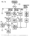
- The processing of the different types of requests issued from an intelligent work station will now be described. With reference first to Figures 5A and 5B showing a flow chart illustrating the operation of the terminal mapping box, the terminal mapping box initially marks all control registers 50 as invalid. This may be accomplished, e.g., during an initialization routine on power-up. The TMB then waits for a request from its work station. Upon receiving a request for a new capability, the TMB at
step 100 forwards a request to the CSP for a new space in the shared memory to be set aside for a particular type of access by the requesting station. As shown in Figure 7A, the CSP at step 200 then selects an unused capability number and associated logical address and atstep 202 forwards a request to theCMCU 34 to identify an available physical address in the sharedmemory 12. If theCMCU 34 does not grant this request, e.g., if there is insufficient shared memory space available, the CSP atstep 206 will return a status error code to the TMB. Upon receiving this error code atstep 102 in Figure 5A, the TMB will advance to step 104 and will interrupt the requesting terminal with a status error code. The requesting terminal can then repeat its request either immediately or at some later time. - If the request by the CSP for a new physical address from the CMCU is granted at
step 204 in Figure 7A, the CSP will receive the MS Port and physical address from the CMCU. Atstep 208, the CSP will choose one of the MMB's to service future requests for this capability, and atstep 210 the CSP will then inform the CMCU that a particular combination of (MMB, LA) translates to (MS Port, PA). The CMCU will then enter this information in a master table. - At
step 212 in Figure 7B, the CSP will then inform the chosen MMB of the translation data from logical address to MS Port and physical address to be entered into its map table, and at step 214 the CSP finally informs the TMB of the translation data for mapping the requested capability to a TS Port and logical address. Upon detecting atstep 102 in Figure 5A that its request has been granted, the TMB updates its map table to include the new capability and loads the new capability into the appropriate control register. That control register is then marked as valid. - A second type of request issued by the intelligent work station is a request for an "existing" capability which is already available to the work station. In such a case, the station loads the desired capability into the appropriate contral register and the TMB checks its map table 48 at
step 106 to verify that the capability is available. If the availability is confirmed, the control register is then marked as valid. If the comparison with the map table 48 yields a negative result, the TMB request the CSP for a TS Port, logical address and corresponding access right atstep 110. The CSP, atstep 216 in Figure 7A, examines the master capability table to determine if the requested capability is one that has already been made available to the requesting intelligent work station. If not, a status error code is returned to the TMB atstep 218, is detected by the TMB atstep 112 in Figure 5A, and the work station is interrupted with a status error code atstep 114. - If the CSP determines from its capability table that the requested capability is available to the requesting work station, the CSP provides the map table data to the TMB at
step 220. The TMB, atstep 116 in Figure 5B, updates its map table 48 and marks the control register as valid. If the TMB notes that it has been asked to load, e.g., a write capability into a DR register, the status register would not indicate a successful load, and an error code would be sent back to the requesting station. - The above description concerns a request by the intelligent work station for a new capability or a request for an existing capability not currently stored in a
control register 50. Once either of these two processes have been completed, the shared memory can be accessed by the work station by merely providing the access address to the TMB. More particularly, with reference to Figure 5A, the TMB will receive from the work station an access address designating a register and an offset. The TMB atstep 120 will examine the addressed control register to determine whether or not it has been marked as valid, and if it is not valid an error code is sent back to the work station to indicate to the station that it must first submit a request to load a desired capability into the register. If the register contents are valid, i.e., if the register contains a capability value which has already been approved by the CSP, the TMB consults its map table 48 and substitutes a TS Port and logical address for the portion of the virtual address from the intelligent work station which designated the register. The TMB atstep 120 forwards the TS Port, logical address and offset to the terminal switch 16 which establishes a connection between the TMB and designated TS Port, so that the logical address and offset are forwarded to the corresponding MMB. - At
step 306 in Figure 6, the MMB examines its own map table to determine if the received logical address is resident. It is possible that, although an area in the shared memory has been set aside for this assigned capability, the CMCU may have found it necessary to make this reserved memory area available for some other purpose. In such a case, the CMCU will have written any data in this memory area out to its backing store and will have deleted the corresponding entry from the appropriate MMB map table. If the MMB finds atstep 306 that the requested logical address is not resident in its map table, it will open a connection to the CMCU atstep 308 and atstep 310 will request the CMCU for new translation data. TheCMCU 34 asynchronously determines and initiates the 1/0 operations needed to make the requested data resident, and this can preferably be accomplished by using an asynchronous array of microprocessors in the CMCU as described in more detail in said copending application Serial No. 567,304. The CMCU will retrieve the data from the backing store and will place it in the sharedmemory 12 and will then inform the MMB of the MS Port and physical address at which the desired data can be accessed. Atstep 312 in Figure 6, the MMB updates its map table with the new translation data. - After the MMB map table has been appropriately updated at
step 312, or if the logical address is originally found in the map table instep 306, the MMB substitutes the corresponding MS Port and physical address for the received logical address, and establishes a connection to the indicated MS Port in thememory switch 20. Atstep 316, the MMB accesses the memory location defined by the physical address and offset, e.g., with the physical address indicating the beginning of a block of memory in which the requested record can be found, and the offset indicating the position within that block, as is common in the art. After the desired memory location has been accessed, the TMB proceeds as illustrated in Figure 5B, i.e., writing to the memory location atstep 122 or reading from the memory location atstep 124 and waiting for the return of data. - A final category of request from the intelligent work station to its TMB may be a request to delete an existing capability which is determined to be no longer necessary, thereby freeing up memory capacity in the shared
memory 12. As shown in Figure 5A, upon receiving a request from its wcrk station to release an existing capability, the TMB atstep 128 will delete the corresponding entry from its map table. Atstep 130, the CSP is notified of the deletion, and the CSP operates as illustrated at steps 224-228 in Figure 7A, i.e., deleting the capability from its own map table and informing the CMCU and appropriate MMB that the logical address translation data should be deleted from their tables. Atstep 132 in Figure 5A, the TMB determines if the capability to be deleted is currently in a control register. If so, that register is marked as invalid. - In addition to the request for access from the intelligent work stations, the
CSP 36 may also process requests for block transfers, as shown in Figure 7A. In response to such a request from mainframe processor 38 identifying a particular MS port, physical address and block size, the CSP opens a channel to the indicated MS Port through thememory switch 20 and implements the block transfer. - A further improvement according to the present invention may reside in the physical location of the various system components. Since data transfers between the shared memory and the microprocessors in the intelligent work stations may advantageously occur at a relative high rate, e.g., 1 megabyte per second, or 10 megabytes per second, it would be advantageous to minimize the length of this data transfer path due to the relatively high cost of transmission media capable of carrying data at such high rates. Thus, the system could be arranged with the shared
memory 12,mapping boxes CMCU 34,CSP 36 and the microprocessor portion of eachintelligent work station 10 all centrally located to minimize their data transfer paths. Keyboard and display combinations can be located at various remote locations and connected to the central location via data transfer lines of significantly greater length. However, since the data transfer between the keyboard/monitor combination and the remainder of the data processing system need only occur at relatively low data rates such as 2400 or 9600 bytes per second, a significant cost savings could be achieved. A further advantage that all system components requiring a higher degree of maintenance would be centrally located while only the low-maintenance keyboard and display would be remotely located. - The above-described local network of distributed processors is memory coupled, permits memory- mapped 1/0 to shared files that are buffered within the system, provides capability accessing of a remotely located data base, permits on-line reconfiguration of all resources, and can be implemented using existing technology. The bandwidth of each switch connection is driven only by the speed of the IT microprocessor, and the system permits extended local processing unencumbered by local storage limitations while also providing a significant cost/performance edge over insertion-ring or broadcast-networks.
- 1/6 accesses to shared files are buffered centrally within the interconnect system rather than funneled through a remote file server. This permits hierarchical staging and isolation of I/0 accesses, without loss of integrity, due to the capability mechanism provided by the mapping boxes and central address-space allocation.
- The interface between this type of memory-coupled network and conventional data-base systems is much simpler and more efficient than gateway-coupled ring networks due to the centralization of control information. Direct support of capability addressing facilitates off-loading of data-base integrity checks, etc.
- In a further modification, the system could be designed for shared capabilities, e.g., one terminal writing information into the shared memory could indicate that all other terminals in system may be given read access to that data, or it could indicate that only certain terminals or terminals provided the required password could have access. The CSP would store information indicating to which intelligent work stations each capability is available, and the CSP would also preferably maintain a record of how many stations were using the capability at any given time. If the station creating the capability subsequently requested that it be released, the CSP would not only have to delete the capability from its table but would have to ensure that the capability was deleted from all terminal mapping box translation tables. Steps 224-228 in Figure 7A would then only be performed if the use counter indicated that the capability being released was no longer in use by any work stations, so that the logical address translation data would not be needed.
Claims (7)
Applications Claiming Priority (2)
| Application Number | Priority Date | Filing Date | Title |
|---|---|---|---|
| US06/626,260 US4710868A (en) | 1984-06-29 | 1984-06-29 | Interconnect scheme for shared memory local networks |
| US626260 | 1984-06-29 |
Publications (3)
| Publication Number | Publication Date |
|---|---|
| EP0166268A2 true EP0166268A2 (en) | 1986-01-02 |
| EP0166268A3 EP0166268A3 (en) | 1987-11-11 |
| EP0166268B1 EP0166268B1 (en) | 1990-05-16 |
Family
ID=24509631
Family Applications (1)
| Application Number | Title | Priority Date | Filing Date |
|---|---|---|---|
| EP85106825A Expired - Lifetime EP0166268B1 (en) | 1984-06-29 | 1985-06-03 | Shared memory access for data processing system |
Country Status (5)
| Country | Link |
|---|---|
| US (1) | US4710868A (en) |
| EP (1) | EP0166268B1 (en) |
| JP (1) | JPS6118053A (en) |
| CA (1) | CA1229422A (en) |
| DE (1) | DE3577761D1 (en) |
Cited By (5)
| Publication number | Priority date | Publication date | Assignee | Title |
|---|---|---|---|---|
| EP0341905A2 (en) * | 1988-05-13 | 1989-11-15 | AT&T Corp. | Computer with intelligent memory system |
| EP0374338A1 (en) * | 1988-12-23 | 1990-06-27 | International Business Machines Corporation | Shared intelligent memory for the interconnection of distributed micro processors |
| EP0387644A1 (en) * | 1989-03-15 | 1990-09-19 | BULL HN INFORMATION SYSTEMS ITALIA S.p.A. | Multiprocessor system with global data replication and two levels of address translation units |
| WO1994025920A1 (en) * | 1993-04-30 | 1994-11-10 | Cray Research, Inc. | Variable latency processor to memory interconnect network |
| EP0730237A1 (en) * | 1995-02-28 | 1996-09-04 | Nec Corporation | Multi-processor system with virtually addressable communication registers and controlling method thereof |
Families Citing this family (54)
| Publication number | Priority date | Publication date | Assignee | Title |
|---|---|---|---|---|
| JPS6289149A (en) * | 1985-10-15 | 1987-04-23 | Agency Of Ind Science & Technol | Multi-port memory system |
| JPS63170780A (en) * | 1986-10-03 | 1988-07-14 | インタランド・コーポレーション | Integrated multi-display type overlay control system communication work station |
| US5054096A (en) * | 1988-10-24 | 1991-10-01 | Empire Blue Cross/Blue Shield | Method and apparatus for converting documents into electronic data for transaction processing |
| US5829002A (en) * | 1989-02-15 | 1998-10-27 | Priest; W. Curtiss | System for coordinating information transfer and retrieval |
| US5163131A (en) * | 1989-09-08 | 1992-11-10 | Auspex Systems, Inc. | Parallel i/o network file server architecture |
| JP2945757B2 (en) * | 1989-09-08 | 1999-09-06 | オースペックス システムズ インコーポレイテッド | Multi-device operating system architecture. |
| US5075846A (en) * | 1989-09-29 | 1991-12-24 | Motorola, Inc. | Memory access serialization as an MMU page attribute |
| EP0453863A2 (en) * | 1990-04-27 | 1991-10-30 | National Semiconductor Corporation | Methods and apparatus for implementing a media access control/host system interface |
| DE69129960T2 (en) * | 1990-09-18 | 1998-12-24 | Fujitsu Ltd | System for designing a shared memory |
| US5544317A (en) * | 1990-11-20 | 1996-08-06 | Berg; David A. | Method for continuing transmission of commands for interactive graphics presentation in a computer network |
| US5182554A (en) * | 1990-12-18 | 1993-01-26 | International Business Machines Corporation | Third party evavesdropping for bus control |
| JPH04310157A (en) * | 1991-04-09 | 1992-11-02 | Chubu Nippon Denki Software Kk | Message repeating system for distributed processing system |
| JPH0581216A (en) * | 1991-09-20 | 1993-04-02 | Hitachi Ltd | Parallel processor |
| US7174352B2 (en) | 1993-06-03 | 2007-02-06 | Network Appliance, Inc. | File system image transfer |
| US6138126A (en) | 1995-05-31 | 2000-10-24 | Network Appliance, Inc. | Method for allocating files in a file system integrated with a raid disk sub-system |
| US6604118B2 (en) | 1998-07-31 | 2003-08-05 | Network Appliance, Inc. | File system image transfer |
| DE69431186T2 (en) * | 1993-06-03 | 2003-05-08 | Network Appliance Inc | Method and file system for assigning file blocks to storage space in a RAID disk system |
| DK0702815T3 (en) * | 1993-06-03 | 2000-12-18 | Network Appliance Inc | Set up a file system for writing at any location |
| DE69434381T2 (en) * | 1993-06-04 | 2006-01-19 | Network Appliance, Inc., Sunnyvale | A method of parity representation in a RAID subsystem using nonvolatile memory |
| JPH0793274A (en) * | 1993-07-27 | 1995-04-07 | Fujitsu Ltd | System and device for transferring data |
| US6101590A (en) * | 1995-10-10 | 2000-08-08 | Micro Unity Systems Engineering, Inc. | Virtual memory system with local and global virtual address translation |
| US5754791A (en) * | 1996-03-25 | 1998-05-19 | I-Cube, Inc. | Hierarchical address translation system for a network switch |
| JP3400916B2 (en) * | 1996-07-11 | 2003-04-28 | 株式会社日立製作所 | Server address management method |
| US6457130B2 (en) | 1998-03-03 | 2002-09-24 | Network Appliance, Inc. | File access control in a multi-protocol file server |
| US6317844B1 (en) | 1998-03-10 | 2001-11-13 | Network Appliance, Inc. | File server storage arrangement |
| US6119244A (en) | 1998-08-25 | 2000-09-12 | Network Appliance, Inc. | Coordinating persistent status information with multiple file servers |
| US6343984B1 (en) | 1998-11-30 | 2002-02-05 | Network Appliance, Inc. | Laminar flow duct cooling system |
| US6295571B1 (en) | 1999-03-19 | 2001-09-25 | Times N Systems, Inc. | Shared memory apparatus and method for multiprocessor systems |
| WO2001028179A2 (en) | 1999-10-14 | 2001-04-19 | Bluearc Uk Limited | Apparatus and method for hardware implementation or acceleration of operating system functions |
| US7308512B1 (en) | 2001-05-16 | 2007-12-11 | Network Appliance, Inc. | Fiber channel adaptor for serial or parallel ATA disks |
| US7218636B2 (en) * | 2001-06-13 | 2007-05-15 | Inrange Technology Corporation | Method and apparatus for rendering a cell-based switch useful for frame based application protocols |
| US7042842B2 (en) * | 2001-06-13 | 2006-05-09 | Computer Network Technology Corporation | Fiber channel switch |
| US7260104B2 (en) * | 2001-12-19 | 2007-08-21 | Computer Network Technology Corporation | Deferred queuing in a buffered switch |
| US7072298B2 (en) * | 2001-06-13 | 2006-07-04 | Computer Network Technology Corporation | Method and apparatus for rendering a cell-based switch useful for frame based protocols |
| JP4014923B2 (en) * | 2002-04-30 | 2007-11-28 | 株式会社日立製作所 | Shared memory control method and control system |
| JP2004110367A (en) | 2002-09-18 | 2004-04-08 | Hitachi Ltd | Storage system control method, storage control device, and storage system |
| US8041735B1 (en) | 2002-11-01 | 2011-10-18 | Bluearc Uk Limited | Distributed file system and method |
| US7457822B1 (en) | 2002-11-01 | 2008-11-25 | Bluearc Uk Limited | Apparatus and method for hardware-based file system |
| US7263593B2 (en) | 2002-11-25 | 2007-08-28 | Hitachi, Ltd. | Virtualization controller and data transfer control method |
| JP2004220450A (en) | 2003-01-16 | 2004-08-05 | Hitachi Ltd | Storage device, its introduction method and its introduction program |
| JP2005018193A (en) | 2003-06-24 | 2005-01-20 | Hitachi Ltd | Interface command control method for disk device, and computer system |
| JP4386694B2 (en) | 2003-09-16 | 2009-12-16 | 株式会社日立製作所 | Storage system and storage control device |
| JP4307202B2 (en) | 2003-09-29 | 2009-08-05 | 株式会社日立製作所 | Storage system and storage control device |
| JP2005202893A (en) | 2004-01-19 | 2005-07-28 | Hitachi Ltd | Storage device controller, storage system, recording medium recording program, information processor, and method for controlling storage system |
| US7623519B2 (en) * | 2004-06-21 | 2009-11-24 | Brocade Communication Systems, Inc. | Rule based routing in a switch |
| US20060013135A1 (en) * | 2004-06-21 | 2006-01-19 | Schmidt Steven G | Flow control in a switch |
| US20050281282A1 (en) * | 2004-06-21 | 2005-12-22 | Gonzalez Henry J | Internal messaging within a switch |
| JP5007485B2 (en) * | 2004-08-26 | 2012-08-22 | ソニー株式会社 | Semiconductor memory device, its access method, and memory control system |
| JP4646574B2 (en) | 2004-08-30 | 2011-03-09 | 株式会社日立製作所 | Data processing system |
| JP2006127028A (en) | 2004-10-27 | 2006-05-18 | Hitachi Ltd | Memory system and storage controller |
| JP5022740B2 (en) * | 2007-03-09 | 2012-09-12 | 矢崎総業株式会社 | Relay connector unit, wire harness assembly, and electronic device control system |
| US7941637B2 (en) * | 2008-04-15 | 2011-05-10 | Freescale Semiconductor, Inc. | Groups of serially coupled processor cores propagating memory write packet while maintaining coherency within each group towards a switch coupled to memory partitions |
| KR20090128814A (en) * | 2008-06-11 | 2009-12-16 | 삼성전자주식회사 | Port selector, device test system and method using the same |
| KR102563760B1 (en) * | 2018-02-22 | 2023-08-07 | 에스케이하이닉스 주식회사 | Interface unit and operating method thereof |
Citations (6)
| Publication number | Priority date | Publication date | Assignee | Title |
|---|---|---|---|---|
| GB1170586A (en) * | 1965-11-16 | 1969-11-12 | Gen Electric | Data Processing System |
| US3634830A (en) * | 1969-06-13 | 1972-01-11 | Ibm | Modular computer sharing system with intercomputer communication control apparatus |
| US3896419A (en) * | 1974-01-17 | 1975-07-22 | Honeywell Inf Systems | Cache memory store in a processor of a data processing system |
| DE2523686A1 (en) * | 1975-05-28 | 1976-12-02 | Siemens Ag | DEVICE AND PROCEDURE FOR ADDRESS TRANSLATION IN A MULTIPROCESSOR SYSTEM WITH VIRTUAL ADDRESSING |
| US4149242A (en) * | 1977-05-06 | 1979-04-10 | Bell Telephone Laboratories, Incorporated | Data interface apparatus for multiple sequential processors |
| EP0024288A2 (en) * | 1979-08-21 | 1981-03-04 | International Business Machines Corporation | Computer system having at least two processors with shared storage |
Family Cites Families (28)
| Publication number | Priority date | Publication date | Assignee | Title |
|---|---|---|---|---|
| US3419849A (en) * | 1962-11-30 | 1968-12-31 | Burroughs Corp | Modular computer system |
| US3444525A (en) * | 1966-04-15 | 1969-05-13 | Gen Electric | Centrally controlled multicomputer system |
| US3492654A (en) * | 1967-05-29 | 1970-01-27 | Burroughs Corp | High speed modular data processing system |
| US3560934A (en) * | 1969-06-10 | 1971-02-02 | Ibm | Arrangement for effecting vector mode operation in multiprocessing systems |
| BE758813A (en) * | 1969-11-28 | 1971-04-16 | Burroughs Corp | PROGRAM STRUCTURES FOR THE IMPLEMENTATION OF INFORMATION PROCESSING SYSTEMS COMMON TO HIGHER LEVEL PROGRAM LANGUAGES |
| US3723976A (en) * | 1972-01-20 | 1973-03-27 | Ibm | Memory system with logical and real addressing |
| US3787816A (en) * | 1972-05-12 | 1974-01-22 | Burroughs Corp | Multiprocessing system having means for automatic resource management |
| US3854126A (en) * | 1972-10-10 | 1974-12-10 | Digital Equipment Corp | Circuit for converting virtual addresses into physical addresses |
| US3905023A (en) * | 1973-08-15 | 1975-09-09 | Burroughs Corp | Large scale multi-level information processing system employing improved failsaft techniques |
| US3889237A (en) * | 1973-11-16 | 1975-06-10 | Sperry Rand Corp | Common storage controller for dual processor system |
| US4077059A (en) * | 1975-12-18 | 1978-02-28 | Cordi Vincent A | Multi-processing system with a hierarchial memory having journaling and copyback |
| US4084231A (en) * | 1975-12-18 | 1978-04-11 | International Business Machines Corporation | System for facilitating the copying back of data in disc and tape units of a memory hierarchial system |
| JPS52130246A (en) * | 1976-04-24 | 1977-11-01 | Fujitsu Ltd | Memory access control system |
| JPS533029A (en) * | 1976-06-30 | 1978-01-12 | Toshiba Corp | Electronic computer |
| JPS53124943A (en) * | 1977-04-08 | 1978-10-31 | Agency Of Ind Science & Technol | Composite information processor |
| US4145739A (en) * | 1977-06-20 | 1979-03-20 | Wang Laboratories, Inc. | Distributed data processing system |
| FR2400729A1 (en) * | 1977-08-17 | 1979-03-16 | Cii Honeywell Bull | DEVICE FOR THE TRANSFORMATION OF VIRTUAL ADDRESSES INTO PHYSICAL ADDRESSES IN A DATA PROCESSING SYSTEM |
| US4155119A (en) * | 1977-09-21 | 1979-05-15 | Sperry Rand Corporation | Method for providing virtual addressing for externally specified addressed input/output operations |
| US4136386A (en) * | 1977-10-06 | 1979-01-23 | International Business Machines Corporation | Backing store access coordination in a multi-processor system |
| US4285040A (en) * | 1977-11-04 | 1981-08-18 | Sperry Corporation | Dual mode virtual-to-real address translation mechanism |
| JPS54111726A (en) * | 1978-02-22 | 1979-09-01 | Hitachi Ltd | Control unit for multiplex virtual memory |
| US4245306A (en) * | 1978-12-21 | 1981-01-13 | Burroughs Corporation | Selection of addressed processor in a multi-processor network |
| US4253146A (en) * | 1978-12-21 | 1981-02-24 | Burroughs Corporation | Module for coupling computer-processors |
| US4240143A (en) * | 1978-12-22 | 1980-12-16 | Burroughs Corporation | Hierarchical multi-processor network for memory sharing |
| US4394649A (en) * | 1980-07-28 | 1983-07-19 | I/O Corporation | Communication terminal providing user communication of high comprehension |
| US4394731A (en) * | 1980-11-10 | 1983-07-19 | International Business Machines Corporation | Cache storage line shareability control for a multiprocessor system |
| JPS57162048A (en) * | 1981-03-31 | 1982-10-05 | Toshiba Corp | Common memory device interface |
| JPS58154059A (en) * | 1982-03-08 | 1983-09-13 | Omron Tateisi Electronics Co | Memory access system of parallel processing system |
-
1984
- 1984-06-29 US US06/626,260 patent/US4710868A/en not_active Expired - Lifetime
-
1985
- 1985-04-16 JP JP60079465A patent/JPS6118053A/en active Granted
- 1985-05-16 CA CA000481723A patent/CA1229422A/en not_active Expired
- 1985-06-03 DE DE8585106825T patent/DE3577761D1/en not_active Expired - Fee Related
- 1985-06-03 EP EP85106825A patent/EP0166268B1/en not_active Expired - Lifetime
Patent Citations (6)
| Publication number | Priority date | Publication date | Assignee | Title |
|---|---|---|---|---|
| GB1170586A (en) * | 1965-11-16 | 1969-11-12 | Gen Electric | Data Processing System |
| US3634830A (en) * | 1969-06-13 | 1972-01-11 | Ibm | Modular computer sharing system with intercomputer communication control apparatus |
| US3896419A (en) * | 1974-01-17 | 1975-07-22 | Honeywell Inf Systems | Cache memory store in a processor of a data processing system |
| DE2523686A1 (en) * | 1975-05-28 | 1976-12-02 | Siemens Ag | DEVICE AND PROCEDURE FOR ADDRESS TRANSLATION IN A MULTIPROCESSOR SYSTEM WITH VIRTUAL ADDRESSING |
| US4149242A (en) * | 1977-05-06 | 1979-04-10 | Bell Telephone Laboratories, Incorporated | Data interface apparatus for multiple sequential processors |
| EP0024288A2 (en) * | 1979-08-21 | 1981-03-04 | International Business Machines Corporation | Computer system having at least two processors with shared storage |
Cited By (10)
| Publication number | Priority date | Publication date | Assignee | Title |
|---|---|---|---|---|
| EP0341905A2 (en) * | 1988-05-13 | 1989-11-15 | AT&T Corp. | Computer with intelligent memory system |
| EP0341905A3 (en) * | 1988-05-13 | 1992-01-22 | AT&T Corp. | Computer with intelligent memory system |
| US5134711A (en) * | 1988-05-13 | 1992-07-28 | At&T Bell Laboratories | Computer with intelligent memory system |
| EP0779584B1 (en) * | 1988-05-13 | 1999-09-29 | AT&T Corp. | Apparatus for storing information for a host processor |
| EP0374338A1 (en) * | 1988-12-23 | 1990-06-27 | International Business Machines Corporation | Shared intelligent memory for the interconnection of distributed micro processors |
| US5148527A (en) * | 1988-12-23 | 1992-09-15 | International Business Machines Corporation | Interface for independently establishing a link and transmitting high level commands including logical addresses from dedicated microprocessor to shared intelligent memory |
| EP0387644A1 (en) * | 1989-03-15 | 1990-09-19 | BULL HN INFORMATION SYSTEMS ITALIA S.p.A. | Multiprocessor system with global data replication and two levels of address translation units |
| WO1994025920A1 (en) * | 1993-04-30 | 1994-11-10 | Cray Research, Inc. | Variable latency processor to memory interconnect network |
| US5623698A (en) * | 1993-04-30 | 1997-04-22 | Cray Research, Inc. | Memory interconnect network having separate routing networks for inputs and outputs using switches with FIFO queues and message steering bits |
| EP0730237A1 (en) * | 1995-02-28 | 1996-09-04 | Nec Corporation | Multi-processor system with virtually addressable communication registers and controlling method thereof |
Also Published As
| Publication number | Publication date |
|---|---|
| DE3577761D1 (en) | 1990-06-21 |
| JPH0449143B2 (en) | 1992-08-10 |
| CA1229422A (en) | 1987-11-17 |
| US4710868A (en) | 1987-12-01 |
| EP0166268B1 (en) | 1990-05-16 |
| EP0166268A3 (en) | 1987-11-11 |
| JPS6118053A (en) | 1986-01-25 |
Similar Documents
| Publication | Publication Date | Title |
|---|---|---|
| EP0166268B1 (en) | Shared memory access for data processing system | |
| US5530902A (en) | Data packet switching system having DMA controller, service arbiter, buffer type managers, and buffer managers for managing data transfer to provide less processor intervention | |
| US5574862A (en) | Multiprocessing system with distributed input/output management | |
| US5680570A (en) | Memory system with dynamically allocatable non-volatile storage capability | |
| US6920519B1 (en) | System and method for supporting access to multiple I/O hub nodes in a host bridge | |
| US5117350A (en) | Memory address mechanism in a distributed memory architecture | |
| US6779077B1 (en) | Virtual tape libraries | |
| US4881164A (en) | Multi-microprocessor for controlling shared memory | |
| EP0485507B1 (en) | Modular input/output system for supercomputers | |
| US4695948A (en) | Bus to bus converter using a RAM for multiple address mapping | |
| US5029074A (en) | Bus adapter unit for digital processing system | |
| US6098149A (en) | Method and apparatus for extending commands in a cached disk array | |
| US5146605A (en) | Direct control facility for multiprocessor network | |
| US5148527A (en) | Interface for independently establishing a link and transmitting high level commands including logical addresses from dedicated microprocessor to shared intelligent memory | |
| US5708784A (en) | Dual bus computer architecture utilizing distributed arbitrators and method of using same | |
| US6055547A (en) | Shared file allocation and release | |
| CA1303229C (en) | Bus adapter unit for digital data processing system | |
| GB2086625A (en) | Disc intercommunication system | |
| US5530904A (en) | System for tranferring data from one communication line to another using a multiplexer for selecting the lines and transferring data without intervention of a main processor | |
| US6961837B2 (en) | Method and apparatus for address translation pre-fetch | |
| US5802557A (en) | System and method for caching information in a digital data storage subsystem | |
| GB2221066A (en) | Address translation for I/O controller | |
| EP0147656B1 (en) | Multi-microprocessor for controlling shared memory | |
| EP0316251B1 (en) | Direct control facility for multiprocessor network | |
| EP0464637B1 (en) | Expanded memory unit |
Legal Events
| Date | Code | Title | Description |
|---|---|---|---|
| PUAI | Public reference made under article 153(3) epc to a published international application that has entered the european phase |
Free format text: ORIGINAL CODE: 0009012 |
|
| AK | Designated contracting states |
Designated state(s): DE FR GB |
|
| 17P | Request for examination filed |
Effective date: 19860424 |
|
| PUAL | Search report despatched |
Free format text: ORIGINAL CODE: 0009013 |
|
| AK | Designated contracting states |
Kind code of ref document: A3 Designated state(s): DE FR GB |
|
| 17Q | First examination report despatched |
Effective date: 19890817 |
|
| GRAA | (expected) grant |
Free format text: ORIGINAL CODE: 0009210 |
|
| AK | Designated contracting states |
Kind code of ref document: B1 Designated state(s): DE FR GB |
|
| REF | Corresponds to: |
Ref document number: 3577761 Country of ref document: DE Date of ref document: 19900621 |
|
| ET | Fr: translation filed | ||
| PLBE | No opposition filed within time limit |
Free format text: ORIGINAL CODE: 0009261 |
|
| STAA | Information on the status of an ep patent application or granted ep patent |
Free format text: STATUS: NO OPPOSITION FILED WITHIN TIME LIMIT |
|
| 26N | No opposition filed | ||
| PGFP | Annual fee paid to national office [announced via postgrant information from national office to epo] |
Ref country code: GB Payment date: 19960520 Year of fee payment: 12 |
|
| PGFP | Annual fee paid to national office [announced via postgrant information from national office to epo] |
Ref country code: FR Payment date: 19960607 Year of fee payment: 12 |
|
| PGFP | Annual fee paid to national office [announced via postgrant information from national office to epo] |
Ref country code: DE Payment date: 19960628 Year of fee payment: 12 |
|
| PG25 | Lapsed in a contracting state [announced via postgrant information from national office to epo] |
Ref country code: GB Effective date: 19970603 |
|
| GBPC | Gb: european patent ceased through non-payment of renewal fee |
Effective date: 19970603 |
|
| PG25 | Lapsed in a contracting state [announced via postgrant information from national office to epo] |
Ref country code: FR Free format text: LAPSE BECAUSE OF NON-PAYMENT OF DUE FEES Effective date: 19980227 |
|
| PG25 | Lapsed in a contracting state [announced via postgrant information from national office to epo] |
Ref country code: DE Free format text: LAPSE BECAUSE OF NON-PAYMENT OF DUE FEES Effective date: 19980303 |
|
| REG | Reference to a national code |
Ref country code: FR Ref legal event code: ST |
|
| REG | Reference to a national code |
Ref country code: FR Ref legal event code: ST |