EP0189523B1 - Microprocessor system - Google Patents
Microprocessor system Download PDFInfo
- Publication number
- EP0189523B1 EP0189523B1 EP85112374A EP85112374A EP0189523B1 EP 0189523 B1 EP0189523 B1 EP 0189523B1 EP 85112374 A EP85112374 A EP 85112374A EP 85112374 A EP85112374 A EP 85112374A EP 0189523 B1 EP0189523 B1 EP 0189523B1
- Authority
- EP
- European Patent Office
- Prior art keywords
- address
- memory
- microprocessor
- instruction
- data
- Prior art date
- Legal status (The legal status is an assumption and is not a legal conclusion. Google has not performed a legal analysis and makes no representation as to the accuracy of the status listed.)
- Expired - Lifetime
Links
Images


Classifications
-
- G—PHYSICS
- G06—COMPUTING; CALCULATING OR COUNTING
- G06F—ELECTRIC DIGITAL DATA PROCESSING
- G06F13/00—Interconnection of, or transfer of information or other signals between, memories, input/output devices or central processing units
-
- G—PHYSICS
- G11—INFORMATION STORAGE
- G11C—STATIC STORES
- G11C11/00—Digital stores characterised by the use of particular electric or magnetic storage elements; Storage elements therefor
- G11C11/21—Digital stores characterised by the use of particular electric or magnetic storage elements; Storage elements therefor using electric elements
- G11C11/34—Digital stores characterised by the use of particular electric or magnetic storage elements; Storage elements therefor using electric elements using semiconductor devices
- G11C11/40—Digital stores characterised by the use of particular electric or magnetic storage elements; Storage elements therefor using electric elements using semiconductor devices using transistors
- G11C11/41—Digital stores characterised by the use of particular electric or magnetic storage elements; Storage elements therefor using electric elements using semiconductor devices using transistors forming static cells with positive feedback, i.e. cells not needing refreshing or charge regeneration, e.g. bistable multivibrator or Schmitt trigger
- G11C11/413—Auxiliary circuits, e.g. for addressing, decoding, driving, writing, sensing, timing or power reduction
- G11C11/417—Auxiliary circuits, e.g. for addressing, decoding, driving, writing, sensing, timing or power reduction for memory cells of the field-effect type
- G11C11/419—Read-write [R-W] circuits
-
- G—PHYSICS
- G06—COMPUTING; CALCULATING OR COUNTING
- G06F—ELECTRIC DIGITAL DATA PROCESSING
- G06F13/00—Interconnection of, or transfer of information or other signals between, memories, input/output devices or central processing units
- G06F13/38—Information transfer, e.g. on bus
- G06F13/40—Bus structure
- G06F13/4004—Coupling between buses
- G06F13/4009—Coupling between buses with data restructuring
- G06F13/4018—Coupling between buses with data restructuring with data-width conversion
-
- G—PHYSICS
- G06—COMPUTING; CALCULATING OR COUNTING
- G06F—ELECTRIC DIGITAL DATA PROCESSING
- G06F15/00—Digital computers in general; Data processing equipment in general
Definitions
- the present invention relates to a microprocessor system configured by connecting a memory and/or I/O having an n/2-bit data bus width to a microprocessor having an n-bit data bus width.
- a programmer must create a program by considering combinations of the architecture of the system and executable instructions (1-/2-/4-byte access instructions or the like). Since a word transfer instruction cannot be used in the 8-bit peripheral control LSI, existing software for 16-bit microprocessors must be rewritten such that a 16-bit word instruction is replaced with two byte transfer instructions.
- Fig. 1 is a block diagram of a conventional microprocessor system.
- the system comprises a microprocessor ( ⁇ CPU 8086) 1, a bus controller (BUS CTRLR) 2, a latch (LATCH) 3, a bus transceiver (TRANSCEIVER) 4, a memory and/or I/O (MEMORY AND/OR I/O) (to be referred to as a memory hereinafter) 5 having a 16-bit data bus width, and a system bus 6.
- the microprocessor 1 comprises, for example, a microprocessor 8086 available from Intel Corp., U.S.A.
- the microprocessor 1 receives a clock CLK and sends status data STS1 to the controller 2.
- the controller 2 Upon reception of the data STS1, the controller 2 supplies a read/write control signal STS to the memory 5 or the like.
- the microprocessor 1 is connected to the latch 3 and the transceiver 4 through an address data bus ADR/DAT.
- the microprocessor 1 supplies an address signal to the latch 3 and a data signal to the transceiver 4.
- the latch 3 receives the address signal from the microprocessor and supplies an address ADDR to the memory 5.
- the transceiver 4 is connected to the memory 5 through a data bus DATA and the bus 6, and transfers data from or to the memory 5.
- the controller 2 supplies a signal ALE to the latch 3 and a signal BDCTL to the transceiver 4.
- the signal ALE controls a latch timing of the address, and the signal BDCTL controls the input/output of the transceiver 4.
- Figs. 2A to 2E are timing charts explaining a read cycle word transfer instruction starting from an even address in the circuit of Fig. 1.
- the machine cycle basically consists of clocks (CLK) T1, T2, T3 and T4, as shown in Fig. 2A.
- the microprocessor 1 In the read cycle starting from the even address, the microprocessor 1 generates the address and the status data in response to the clock T1, as shown in Fig. 2B.
- the controller 2 supplies the signal ALE to the latch 3 in response to the status data, as shown in Fig. 2D.
- the controller 2 supplies the signal STS to the memory 5, as shown in Fig. 2C.
- the latch 3 latches the address in response to the signal ALE generated from the controller 2.
- 16-bit data is read out from the memory 5 onto the bus DATA, and the transceiver 4 sends the 16-bit data shown in Fig. 2B from the memory 5 onto the bus ADR/DAT by the control signal BDCTL shown in Fig. 2E from the bus controller 2.
- the microprocessor 1 fetches the data at the trailing edge of the clock T3.
- the word transfer instruction of the read cycle starting from an odd address there are two access cycles. Data fetching is performed in the same manner as in the read cycle starting from an even address. However, in the first access cycle, the data corresponding to the start even address is fetched as the most significant part of the 16-bit data. The address is then updated, and in the second access cycle, the data corresponding to the start odd address is fetched as the least significant part. In this manner, 16-bit data is thus fetched by the microprocessor 1.
- the above operation can be performed in the same manner as in the word transfer instruction of the write cycle.
- the prior art microprocessor system has a 16-byte boundary. Although one address has 1-byte data, the address has, as its objective, a memory of basically a 16-bit data bus width. For this reason, the microprocessor system configuration is not flexible, resulting in inconvenience (see MEMORY ORGANIZATION of MICROPROCESSOR AND PERIPHERALS HANDBOOK 1983 published by Intel Corp. for further reference).
- This method comprises the steps of: (a) extracting a read/write control signal for said memory and/or I/O from status data generated from said microprocessor when said microprocessor executes the word transfer instruction, supplying the read/write control signal together with an address to said memory and/or I/O setting a bus converter for connecting a data bus coupled to said memory and/or I/O with a n-bit data bus width, and starting a first access cycle, and (b) causing said microprocessor to inhibit generation of the read/write control signal to complete the word transfer instruction.
- a first access cycle for said memory and/or I/O is performed said first step comprising: a step of detecting that the instruction executed by said microprocessor is a word transfer instruction for said memory and/or I/O; a step of setting said microprocessor in a wait state before the first access cycle is completed and when the instruction is determined to be the word transfer instruction for said memory and/or I/O; and a step of inhibiting generation of the read/write control signal to complete the first access cycle.
- the address is updated by adding 1 to the address while the read/write control signal is disabled and the updated address is supplied to said memory and/or I/O and the read/write control signal is enabled again to start the second access cycle.
- a second access cycle for said memory and/or I/O is performed the wait state of said microprocessor being cancelled during said second access cycle.
- the present invention provides a microprocessor system and a method as defined in claims 1 and 11, respectively.
- a software programmer need not selectively use the word transfer instruction and the byte transfer instruction in accordance with the data bus width of the memory and/or I/O. In other words, the programmer can always use word transfer instructions.
- Fig. 3 is a block diagram of a microprocessor system configured by connecting a memory and/or I/O 17 having an 8-bit data bus width to a 16-bit microprocessor 11.
- the microprocessor system comprises the microprocessor 11, a read/write controller 12, an address latch counter 13, a timing generator 14, a bus converter 15, a 16-bit memory and/or I/O 16, the 8-bit memory and/or I/O 17, and a system bus 18.
- the timing generator 14 further comprises a detector 19, a counter 20, and a timing controller 21.
- the microprocessor 11 receives a clock CLK and a wait control signal WAIT from the controller 21 and supplies status data STS1 to the controller 12 and an address ADR 19-0 to the counter 13.
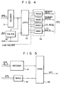
- the controller 12 comprises a decoder 31, a pulser 32, a latch 33 and a gate 34, as shown in Fig. 4.
- the decoder 31 decodes the status data STS1 supplied from the microprocessor 11 and supplies the decoded data to the pulser 32 and the latch 33.
- the pulser 32 supplies an address latch enable signal ALE to the counter 13 in response to the clock CLK.
- the latch 33 latches the outputs from the decoder 31 in response to the clock CLK, and the latched data is supplied to the gate 34.
- the gate 34 supplies, to the detector 19 and the controller 21, a read/write control signal STS representing the memory or I/O write or read mode, and controlled by the control signal COM EN/ DIS from the controller 21 to be described later.
- the gate 34 also supplies the read/write control signal STS to the memories and/or I/Os 16 and 17 through the bus 18.
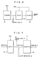
- the address latch counter 13 comprises a latch 61 and a counter 62, as shown in Fig. 7.
- the latch 61 latches the address ADR 19-0 from the microprocessor 11 in response-to the signal ALE from the controller 12.
- An address ADR 19-0 is supplied to the counter 62 and the detector 19.
- the least significant bit ADR 0 of the address is supplied to the controller 21.
- the counter 62 receives, as a preset value, the output from the latch 61, and is counted up in response to a signal of logic "1" from the controller 21.
- the updated address data is supplied from the counter 62 to the memories and/or I/Os 16 and 17 through a bus ADDR 19-0 and the bus 18.
- the detector 19 comprises a decoder 41 and gates 42 and 43, as shown in Fig. 5.
- the decoder 41 decodes the address data ADR 19-0 generated from the counter 13 and supplies the decoded result to the gate 43.
- the gate 42 calculates the NAND product of the read/write control signals STS as outputs from the controller 12 and supplies the NAND signal to the gate 43.
- the gate 43 also calculates the NAND product of the inputs.
- the gate 43 supplies a detection signal DET to the counter 20 and the controller 21.
- the counter 20 comprises a counter 51, a delay 52 and a pulser 53, as shown in Fig. 6.
- the counter 51 counts the output signal DET from the detector 19.
- the counter 51 supplies a signal CYC to the controller 21 and the delay 52.
- the delay 52 receives the output from the counter 51 and the clock signal CLK.
- the delay 52 supplies a signal to the pulser 53.
- the pulser 53 supplies a signal RESET to the controller 21 to reset the controller 21.
- the microprocessor 11 exchanges data with the converter 15 through a data bus DAT.
- the converter 15 comprises bidirectional bus drivers 71, 73 and 75, and latches 72 and 74.
- a set of the driver 71 and the latch 72, and another set of the driver 73 and the latch 74 are connected in parallel between the data buses DAT 15-8 and DATA 15-8, and between the data buses DAT 7-0 and DATA 7-0.
- the latches 72 and 74 are connected to supply data to the microprocessor 11.
- the driver 75 is arranged to connect the bus DATA 15-8 to the bus DATA 7-0.
- the converter 15 receives from the controller 21 control signals BD1EN and BD1DIR for the driver 71, control signals BD2EN and BD2DIR for the driver 73, control signals BD3EN and BD3DIR for the driver 75, control signals LT2CNT and LT2EN for the latch 72, and control signals LT1CNT and LT1EN for the latch 74.
- the memories and/or I/Os 16 and 17 receive the signal STS and an address ADDR.
- a data bus DATA 15-0 is connected to the 16-bit memory and/or I/O 16
- the bus DATA 7-0 is connected to the 8-bit memory and/or I/O 17.
- the memory and/or I/O 17 is connected to a previously assigned address.
- the operation of the microprocessor system of this embodiment will be described with reference to the timing charts of Figs. 9A to 11T.
- the clock signal CLK basically consists of clock pulses T1, T2, T3 and T4.
- TW When the microprocessor 11 is held in the wait state, the clock signal CLK is represented by TW.
- the microprocessor 11 executes the word transfer instruction, it supplies the status STS1 to the controller 12, as shown in Fig. 9B.
- the microprocessor 11 also supplies the address to the address latch counter 13, as shown in Fig. 9E.
- the counter 13 latches the address in response to a latch control signal ALE from the read/write controller 12, as shown in Figs.
- the signals BD1EN , BD2EN , BD3EN and LT1EN are output enable/disable signals.
- the signals BD1DIR, BD2DIR and BD3DIR are output direction control signals.
- the signal is output from the directions A to B illustrated in Fig. 8.
- the signal is output from direction B to direction A when the signal BD1DIR, BD2DIR or BD3DIR is set at a low level.
- the signal LT1CNT is a latch timing control signal.
- the drivers 71 and 73 are operated to supply data from the memories and/or I/Os 16 and 17 to the microprocessor 11.
- the detector 19 detects, in accordance with the read/write control signal and the address, that the instruction is an instruction for the 8-bit memory and/or I/O 17, the detector 19 supplies the DET signal to the controller 21.
- the controller 21 then supplies the signal WAIT to the microprocessor 11, as shown in Fig. 9H, so as to set the microprocessor 11 in the wait state.
- the data from the memory and/or I/O 17 is sent onto the bus DAT 7-0.
- the microprocessor 11 does not fetch data.
- the controller 21 supplies the signal LT1CNT to the latch 74, so that the data on the bus DAT 7-0 is latched by the latch 74.
- the controller 21 supplies the signal BD2EN to the driver 73 to inhibit data output, as shown in Fig. 9P.
- the controller 21 supplies the signal COM EN/ DIS to the controller 12 to inhibit generation of the signal STS .
- the read/write control signal STS is disabled.
- the controller 21 supplies a signal of logic "1" to the counter 62.
- the counter 62 sends the updated address onto an address bus ADDR. As shown in Fig.
- the controller 21 supplies the signal LT1EN to the latch 74.
- the latch 74 sends the data onto the data bus DAT 7-0, as shown in Fig. 9L.
- the controller 21 supplies the signal COM EN/ DIS to the controller 12 to enable generation of the read/write control signal STS .
- the signal STS is enabled again so that the second access cycle can be started.
- the driver 75 supplies the data read out from the memory and/or I/O 17 to the bus DATA 15-8 through the bus DATA 7-0, as shown in Figs. 9J and 9K, in response to the signal BD3EN (Fig. 9R) from the controller 21.
- Figs. 9R the signal BD3EN
- the driver 71 sends the data from the bus DATA 15-8 onto the bus DAT 15-8 in response to the signal BD1EN from the controller 21.
- the 16-bit data appears on the bus DAT 15-0.
- the controller 21 generates the signal WAIT , as shown in Fig. 9H, so that the wait state of the microprocessor 11 is cancelled.
- the microprocessor 11 fetches the 16-bit data and inhibits generation of the data STS1 , as shown in Fig. 9B.
- the signal STS is also inhibited.
- the pulser 53 supplies the signal RESET to the controller 21, as shown in Fig. 91.
- the controller 21 resets the signals BD1EN , BD3EN , LT1CNT and LT1EN , as shown in Figs. 9N, 9R, 9S and 9T, respectively. Subsequently, the controller 21 resets the signals BD1DIR, BD2DIR and BD3DIR (Figs. 9M, 90 and 9Q). In this manner, conversion operation is completed. In a read cycle starting with an even address, the latch 72 is kept disabled.
- a write cycle starting with an even address will be described with reference to Figs. 10A to 10T.
- the clock signal CLK, the data STS1 , the control signal COM EN/ DIS , the read/write control signal STS , the control signal WAIT for the microprocessor 11, the reset signal RESET and the signal of logic "1" are the same as those of the read cycle starting with the even address.
- the signals associated with the converter 15 will mainly be considered in the following description.
- the drivers 71 and 73 are operated to supply 16-bit data to the memory and/or I/O 16, as shown in Figs. 10M, 10N, 100 and 10P. Since the driver 75 is disabled, as shown in Fig.
- the driver 73 supplies data from the bus DAT 7-0 to the bus DATA 7-0, as shown in Fig. 10J. This data is transferred to the memory and/or I/O 17 through the bus DATA 7-0.
- the driver 71 is kept enabled, as shown in Figs. 10M and 10N. However, the driver 73 is disabled, as shown in Fig. 10P. Instead, the driver 75 is enabled, as shown in Fig. 10R. For this reason, the most significant part of the 16-bit data generated from the microprocessor 11 is supplied by the drivers 71 and 75 to the memory and/or I/O 17 through the bus DATA 7-0, as shown in Fig. 10J.
- the latches 72 and 74 are kept disabled. In this manner, the write cycle with the even address is executed.
- the clock signal CLK, the data STS1, the control signal COM EN/ DIS , the read/write control signal STS , the control signal WAIT for the microprocessor 11, the reset signal RESET and the signal of logic "1" are the same as those of a read cycle starting with an even address.
- the signals associated with the converter 15 will be considered in the following description.
- the drivers 71 and 73 are operated to supply the 16-bit data from the memory and/or I/O 16 to the microprocessor 11, as shown in Figs. 11M, 11N, 110 and 11P.
- the converter 75 is held operative, as shown in Figs.
- the data (Fig. 11J) read out from the memory and/or I/O 17, and appearing on the bus DATA 7-0 is sent onto the bus DATA 15-8, as shown in Fig. 11K.
- the drivers 71 and 73 transfer the data from the bus DATA 15-0 to the bus DAT 15-0, as shown in Fig. 11E.
- the microprocessor 11 is held in the wait state, as shown in Fig. 11H, and does not fetch the data.
- the controller 21 supplies the signal LT2CNT to the latch 72, as shown in Fig. 11S, so that the latch 72 latches the data.
- the controller 21 supplies the signal BD1EN and BD3EN to the drivers 71 and 75, as shown in Figs.
- the latch 72 sends the data onto the bus DAT 15-8, as shown in Fig. 11L.
- the driver 73 sends the data read out from the memory and/or I/O 17 onto the bus DAT 7-0, as shown in Fig. 11K. Therefore, as shown in Fig. 11E, the 16-bit data appears on the bus DAT 15-0.
- the wait state of the microprocessor 11 is cancelled in response to the signal WAIT from the controller 21, as shown in Fig. 11H, and the microprocessor 11 fetches the 16-bit data. In this manner, the read cycle starting with the odd address is completed. In the read cycle starting from the odd address, the latch 74 is kept disabled.
- the output CYC from the counter 20 can be omitted when the controller 21 performs sequential operation.
- a read/write word transfer instruction is performed for the memory and/or I/O 16 having the 16-bit data bus width, the operation is performed at timings as shown in Figs. 2A to 2E.
- the microprocessor 11 comprises a 8086 available from Intel Corp.
- the latch 72 in the converter 15 can be omitted.
- a portion for controlling the latch 72 can also be omitted from the controller 21.
- the address latch counter 13 can be simplified, as shown in Fig. 12.
- the counter 13 comprises a latch 81 and a gate 82.
- the latch 81 latches the address from the microprocessor 11 and supplies the least significant bit thereof to the controller 21 and the gate 82.
- the remaining bits of the address are sent from the latch 81 onto an address bus ADDR 19-1.
- the gate 82 calculates a logical OR of the output from the latch 81 and the logic "1" from the controller 21, and generates the sum as the least significant bit of the address data. All bits of the address signal appear on the address bus ADDR and are supplied to the memories and/or I/Os 16 and 17.
- the timing charts of this microprocessor system are the same as those of the word transfer instruction starting with an even address in Figs. 9A to 10T.
- the present invention is exemplified by a microprocessor system configured by connecting an 8-bit memory and/or I/O to a 16-bit microprocessor.
- a 16-bit memory and/or I/O may be connected to a 32-bit microprocessor, or a 32-bit memory and/or I/O may be connected to a 64-bit microprocessor.
Description
- The present invention relates to a microprocessor system configured by connecting a memory and/or I/O having an n/2-bit data bus width to a microprocessor having an n-bit data bus width.
- Semiconductor technology has developed in recent years to allow creation of a high-performance computer system through a combination of a microprocessor and its peripheral control LSIs (DMA controller, etc.), and to the extent that computer systems can be designed with ease. Furthermore, 8-bit microprocessors are gradually being replaced with 16- and 32-bit microprocessors, and microprocessor capability has been reinforced. However, most currently available peripheral control LSIs are operated on an 8-bit operation basis. For example, when a 16-bit microprocessor controls a peripheral control LSI with an 8-bit data bus width, two byte transfer instructions are used in place of one word transfer instruction. In this manner, a programmer must create a program by considering combinations of the architecture of the system and executable instructions (1-/2-/4-byte access instructions or the like). Since a word transfer instruction cannot be used in the 8-bit peripheral control LSI, existing software for 16-bit microprocessors must be rewritten such that a 16-bit word instruction is replaced with two byte transfer instructions.
- The prior art will be described hereinafter. Fig. 1 is a block diagram of a conventional microprocessor system. The system comprises a microprocessor (µCPU 8086) 1, a bus controller (BUS CTRLR) 2, a latch (LATCH) 3, a bus transceiver (TRANSCEIVER) 4, a memory and/or I/O (MEMORY AND/OR I/O) (to be referred to as a memory hereinafter) 5 having a 16-bit data bus width, and a
system bus 6. Themicroprocessor 1 comprises, for example, amicroprocessor 8086 available from Intel Corp., U.S.A. Themicroprocessor 1 receives a clock CLK and sends status data STS1 to thecontroller 2. Upon reception of the data STS1, thecontroller 2 supplies a read/write control signalSTS to thememory 5 or the like. Themicroprocessor 1 is connected to thelatch 3 and thetransceiver 4 through an address data bus ADR/DAT. Themicroprocessor 1 supplies an address signal to thelatch 3 and a data signal to thetransceiver 4. Thelatch 3 receives the address signal from the microprocessor and supplies an address ADDR to thememory 5. Thetransceiver 4 is connected to thememory 5 through a data bus DATA and thebus 6, and transfers data from or to thememory 5. Thecontroller 2 supplies a signal ALE to thelatch 3 and a signal BDCTL to thetransceiver 4. The signal ALE controls a latch timing of the address, and the signal BDCTL controls the input/output of thetransceiver 4. - The operation of the microprocessor system will be described. Figs. 2A to 2E are timing charts explaining a read cycle word transfer instruction starting from an even address in the circuit of Fig. 1. The machine cycle basically consists of clocks (CLK) T1, T2, T3 and T4, as shown in Fig. 2A. In the read cycle starting from the even address, the
microprocessor 1 generates the address and the status data in response to the clock T1, as shown in Fig. 2B. Thecontroller 2 supplies the signal ALE to thelatch 3 in response to the status data, as shown in Fig. 2D. Thecontroller 2 supplies the signalSTS to thememory 5, as shown in Fig. 2C. Thelatch 3 latches the address in response to the signal ALE generated from thecontroller 2. 16-bit data is read out from thememory 5 onto the bus DATA, and thetransceiver 4 sends the 16-bit data shown in Fig. 2B from thememory 5 onto the bus ADR/DAT by the control signal BDCTL shown in Fig. 2E from thebus controller 2. - The
microprocessor 1 fetches the data at the trailing edge of the clock T3. In the word transfer instruction of the read cycle starting from an odd address, there are two access cycles. Data fetching is performed in the same manner as in the read cycle starting from an even address. However, in the first access cycle, the data corresponding to the start even address is fetched as the most significant part of the 16-bit data. The address is then updated, and in the second access cycle, the data corresponding to the start odd address is fetched as the least significant part. In this manner, 16-bit data is thus fetched by themicroprocessor 1. - The above operation can be performed in the same manner as in the word transfer instruction of the write cycle. As is apparent from the above description, the prior art microprocessor system has a 16-byte boundary. Although one address has 1-byte data, the address has, as its objective, a memory of basically a 16-bit data bus width. For this reason, the microprocessor system configuration is not flexible, resulting in inconvenience (see MEMORY ORGANIZATION of MICROPROCESSOR AND PERIPHERALS HANDBOOK 1983 published by Intel Corp. for further reference).
- Prior art document E.D.N. Electrical design news, volume 29,
number 16, 9th August 1984, pages 199 to 206 discloses a method for automatically converting a word transfer instruction to two 1/2-word transfer instructions in a microprocessor system configured by connecting a memory and/or I/O with a n/2-bit data bus width to a microprocessor with a n/-bit data bus width. This method comprises the steps of: (a) extracting a read/write control signal for said memory and/or I/O from status data generated from said microprocessor when said microprocessor executes the word transfer instruction, supplying the read/write control signal together with an address to said memory and/or I/O setting a bus converter for connecting a data bus coupled to said memory and/or I/O with a n-bit data bus width, and starting a first access cycle, and (b) causing said microprocessor to inhibit generation of the read/write control signal to complete the word transfer instruction. Further in a first step a first access cycle for said memory and/or I/O is performed said first step comprising:
a step of detecting that the instruction executed by said microprocessor is a word transfer instruction for said memory and/or I/O;
a step of setting said microprocessor in a wait state before the first access cycle is completed and when the instruction is determined to be the word transfer instruction for said memory and/or I/O; and
a step of inhibiting generation of the read/write control signal to complete the first access cycle. Then the address is updated by adding 1 to the address while the read/write control signal is disabled and the updated address is supplied to said memory and/or I/O and the read/write control signal is enabled again to start the second access cycle. Finally, a second access cycle for said memory and/or I/O is performed the wait state of said microprocessor being cancelled during said second access cycle. - Whereas above E.D.N. document describes an even read cycle and an even write cycle wherein the low byte is first transfered, the address updated by adding 1 to it and then the higher byte is transfered, prior art document COMPUTER DESIGN, vol. 24, no. 1, January 1985, pages 187-194, 196, 198, Littleton, Massachusetts, US; M.S. YOUNG et al.: "Mixing data paths expands options in system design", discloses an odd read cycle and an odd write cycle wherein the higher byte is first transfered.
- It is an object of the present invention to provide microprocessor system and method that can automatically convert a word transfer instruction to two byte transfer instructions.
- To solve this object the present invention provides a microprocessor system and a method as defined in
claims 1 and 11, respectively. - According to the microprocessor system of the present invention, a software programmer need not selectively use the word transfer instruction and the byte transfer instruction in accordance with the data bus width of the memory and/or I/O. In other words, the programmer can always use word transfer instructions.
- This invention can be more fully understood from the following detailed description when taken in conjunction with the accompanying drawings, in which:
- Fig. 1 is a block diagram of a microprocessor system of the prior art;
- Fig. 2A to 2E are timing charts explaining the read cycle starting from an even address in the system of Fig. 1 in which Fig. 2A shows a clock CLK, Fig. 2B shows a state of the address data bus ADR/DAT, Fig. 2C shows the read/write control signal
STS generated from abus controller 2, Fig. 2D shows an address latch control signal ALE generated from thecontroller 2, and Fig. 2E shows a signal BDCTL generated from thecontroller 2 to control thetransceiver 4; - Fig. 3 is a block diagram of a microprocessor system according to an embodiment of the present invention;
- Fig. 4 is a detailed block diagram of a read/write controller in the system shown in Fig. 3;
- Fig. 5 is a detailed block diagram of a detector in the system shown in Fig. 3;
- Fig. 6 is a detailed block diagram of a counter in the system shown in Fig. 3;
- Fig. 7 is a detailed block diagram of an address latch counter in the system shown in Fig. 3;
- Fig. 8 is a detailed block diagram of a bus converter in the system shown in Fig. 3;
- Figs. 9A to 9T, Figs. 10A to 10T and Figs. 11A to 11T are timing charts explaining the word transfer instructions of read, write and read cycles starting from the even, even and odd addresses, respectively, in a microprocessor system configured by connecting a memory and/or I/O having an 8-bit data bus width to a 16-bit microprocessor, in which Figs. 9A, 10A and 11A show clocks CLK, Figs. 9B, 10B and 11B show status data
STS1 generated from the microprocessor, Figs. 9C, 10C and 11C show signals COMEN/DIS for controlling generation of the read/write control signal, Figs. 9D, 10D and 11D show outputsSTS of the read/write control signal, Figs. 9E, 10E and 11E show states of an address data bus ADR/DAT 15-0, Figs. 9F, 10F and 11F show states of an address bus ADDR 19-1, Figs. 9G, 10G and 11G show states of an address bit ADDRO, Figs. 9H, 10H and 11H show signalsWAIT for controlling the waiting states of the microprocessor, Figs. 91, 10I and 11I show signalsRESET for resetting the timing controller, Figs. 9J, 10J and 11J show states of a data bus DATA 7-0, Figs. 9K, 10K, and 11K show states of a data bus DATA 15-8, Figs. 9L and 10L show outputs from alatch 74 while Fig. 11L shows an output from alatch 72, Figs. 9M, 10M and 11M show signals BD1DIR for determining the output directions of abidirectional bus driver 71, Figs. 9N, 10N and 11N show signalsBD1EN for inhibiting output generation of thedriver 71, Figs. 90, 100 and 110 show signals BD2DIR for determining the output direction of abidirectional bus driver 73, Figs. 9P, 10P and 11P show signalsBD2EN for enabling or disabling output generation of thedriver 73, Figs. 9Q, 10Q and 11Q show signals BD3DIR for determining the output direction of abidirectional bus driver 75, Figs. 9R, 10R and 11R show signalsBD3EN for enabling/disabling output generation of thedriver 75, Figs. 9S and 10S show signals LT1CNT for controlling the latch timings of thelatch 74 while Fig. 11S shows a signal LT2CNT for controlling a latch timing of thelatch 72, and Figs. 9T and 10T show signalsLT1EN for controlling generation of data latched by thelatch 74 while Fig. 11T shows a signalLT2EN for controlling generation of data latched by thelatch 72; and - Fig. 12 is a block diagram showing a modification of the address latch counter of Fig. 3.
- The present invention will be described in detail with reference to a preferred embodiment.
- Fig. 3 is a block diagram of a microprocessor system configured by connecting a memory and/or I/
O 17 having an 8-bit data bus width to a 16-bit microprocessor 11. - At first the architecture of the system will be described with reference to Fig. 3. The microprocessor system comprises the microprocessor 11, a read/
write controller 12, anaddress latch counter 13, atiming generator 14, abus converter 15, a 16-bit memory and/or I/O 16, the 8-bit memory and/or I/O 17, and a system bus 18. Thetiming generator 14 further comprises adetector 19, acounter 20, and atiming controller 21. The microprocessor 11 receives a clock CLK and a wait control signalWAIT from thecontroller 21 and supplies status dataSTS1 to thecontroller 12 and an address ADR 19-0 to thecounter 13. Thecontroller 12 comprises adecoder 31, apulser 32, alatch 33 and agate 34, as shown in Fig. 4. Thedecoder 31 decodes the status dataSTS1 supplied from the microprocessor 11 and supplies the decoded data to thepulser 32 and thelatch 33. Thepulser 32 supplies an address latch enable signal ALE to thecounter 13 in response to the clock CLK. Thelatch 33 latches the outputs from thedecoder 31 in response to the clock CLK, and the latched data is supplied to thegate 34. Thegate 34 supplies, to thedetector 19 and thecontroller 21, a read/write control signalSTS representing the memory or I/O write or read mode, and controlled by the control signal COM EN/DIS from thecontroller 21 to be described later. Thegate 34 also supplies the read/write control signalSTS to the memories and/or I/Os - The
address latch counter 13 comprises alatch 61 and acounter 62, as shown in Fig. 7. Thelatch 61 latches the address ADR 19-0 from the microprocessor 11 in response-to the signal ALE from thecontroller 12. An address ADR 19-0 is supplied to thecounter 62 and thedetector 19. The leastsignificant bit ADR 0 of the address is supplied to thecontroller 21. Thecounter 62 receives, as a preset value, the output from thelatch 61, and is counted up in response to a signal of logic "1" from thecontroller 21. The updated address data is supplied from thecounter 62 to the memories and/or I/Os detector 19 comprises adecoder 41 andgates decoder 41 decodes the address data ADR 19-0 generated from thecounter 13 and supplies the decoded result to thegate 43. Thegate 42 calculates the NAND product of the read/write control signalsSTS as outputs from thecontroller 12 and supplies the NAND signal to thegate 43. Thegate 43 also calculates the NAND product of the inputs. When an instruction executed by the microprocessor 11 is determined to be the word transfer instruction for the 8-bit memory and/or I/O 17, thegate 43 supplies a detection signal DET to thecounter 20 and thecontroller 21. Thecounter 20 comprises acounter 51, adelay 52 and apulser 53, as shown in Fig. 6. The counter 51 counts the output signal DET from thedetector 19. When the count of thecounter 51 has reached "2", i.e., when the start of the second access cycle is represented, thecounter 51 supplies a signal CYC to thecontroller 21 and thedelay 52. Thedelay 52 receives the output from thecounter 51 and the clock signal CLK. - When a predetermined period of time has elapsed, the
delay 52 supplies a signal to thepulser 53. Thepulser 53 supplies a signalRESET to thecontroller 21 to reset thecontroller 21. Referring to Fig. 3, the microprocessor 11 exchanges data with theconverter 15 through a data bus DAT. As shown in Fig. 8, theconverter 15 comprisesbidirectional bus drivers driver 71 and thelatch 72, and another set of thedriver 73 and thelatch 74 are connected in parallel between the data buses DAT 15-8 and DATA 15-8, and between the data buses DAT 7-0 and DATA 7-0. In this case, thelatches driver 75 is arranged to connect the bus DATA 15-8 to the bus DATA 7-0. Theconverter 15 receives from thecontroller 21 control signalsBD1EN and BD1DIR for thedriver 71, control signalsBD2EN and BD2DIR for thedriver 73, control signalsBD3EN and BD3DIR for thedriver 75, control signals LT2CNT andLT2EN for thelatch 72, and control signals LT1CNT andLT1EN for thelatch 74. The memories and/or I/Os STS and an address ADDR. A data bus DATA 15-0 is connected to the 16-bit memory and/or I/O 16, and the bus DATA 7-0 is connected to the 8-bit memory and/or I/O 17. The memory and/or I/O 17 is connected to a previously assigned address. - The operation of the microprocessor system of this embodiment will be described with reference to the timing charts of Figs. 9A to 11T. At first a read cycle starting from an even address will be described with reference to Figs. 9A to 9T. The clock signal CLK basically consists of clock pulses T1, T2, T3 and T4. When the microprocessor 11 is held in the wait state, the clock signal CLK is represented by TW. When the microprocessor 11 executes the word transfer instruction, it supplies the status
STS1 to thecontroller 12, as shown in Fig. 9B. The microprocessor 11 also supplies the address to theaddress latch counter 13, as shown in Fig. 9E. Thecounter 13 latches the address in response to a latch control signal ALE from the read/write controller 12, as shown in Figs. 9F and 9G. As shown in Fig. 9C, since signal COM EN/DIS disable a read/write control signal is not generated from thecontroller 21 at this moment, thecontroller 12 generates the signalSTS , as shown in Fig. 9D. Simultaneously, as if the instruction is a read instruction for the 16-bit memory and/or I/O 16, thecontroller 12 generates the bus control signalsBD1EN , BD1DIR,BD2EN , BD2DIR,BD3EN , BD3DIR, LT1CNT andLT1EN as shown in Figs. 9M to 9T. Among these signals, the signalsBD1EN ,BD2EN ,BD3EN andLT1EN are output enable/disable signals. The signals BD1DIR, BD2DIR and BD3DIR are output direction control signals. When one of the signals BD1DIR, BD2DIR or BD3DIR is set at a high level, the signal is output from the directions A to B illustrated in Fig. 8. However, the signal is output from direction B to direction A when the signal BD1DIR, BD2DIR or BD3DIR is set at a low level. The signal LT1CNT is a latch timing control signal. - The
drivers Os detector 19 detects, in accordance with the read/write control signal and the address, that the instruction is an instruction for the 8-bit memory and/or I/O 17, thedetector 19 supplies the DET signal to thecontroller 21. Thecontroller 21 then supplies the signalWAIT to the microprocessor 11, as shown in Fig. 9H, so as to set the microprocessor 11 in the wait state. As shown in Fig. 9E, the data from the memory and/or I/O 17 is sent onto the bus DAT 7-0. However, the microprocessor 11 does not fetch data. As shown in Fig. 9S, thecontroller 21 supplies the signal LT1CNT to thelatch 74, so that the data on the bus DAT 7-0 is latched by thelatch 74. At the same time, thecontroller 21 supplies the signalBD2EN to thedriver 73 to inhibit data output, as shown in Fig. 9P. As shown in Fig. 9C, thecontroller 21 supplies the signal COM EN/DIS to thecontroller 12 to inhibit generation of the signalSTS . As a result, as shown in Fig. 9D, the read/write control signalSTS is disabled. Thecontroller 21 supplies a signal of logic "1" to thecounter 62. Thecounter 62 sends the updated address onto an address bus ADDR. As shown in Fig. 9T, thecontroller 21 supplies the signalLT1EN to thelatch 74. Thelatch 74 sends the data onto the data bus DAT 7-0, as shown in Fig. 9L. Thecontroller 21 supplies the signal COM EN/DIS to thecontroller 12 to enable generation of the read/write control signalSTS . As shown in Fig. 9D, the signalSTS is enabled again so that the second access cycle can be started. Thedriver 75 supplies the data read out from the memory and/or I/O 17 to the bus DATA 15-8 through the bus DATA 7-0, as shown in Figs. 9J and 9K, in response to the signalBD3EN (Fig. 9R) from thecontroller 21. As shown in Figs. 9M and 9N, thedriver 71 sends the data from the bus DATA 15-8 onto the bus DAT 15-8 in response to the signalBD1EN from thecontroller 21. As shown in Fig. 9E, the 16-bit data appears on the bus DAT 15-0. In this case, thecontroller 21 generates the signalWAIT , as shown in Fig. 9H, so that the wait state of the microprocessor 11 is cancelled. The microprocessor 11 fetches the 16-bit data and inhibits generation of the dataSTS1 , as shown in Fig. 9B. As a result, as shown in Fig. 9D, the signalSTS is also inhibited. Thepulser 53 supplies the signalRESET to thecontroller 21, as shown in Fig. 91. Thecontroller 21 resets the signalsBD1EN ,BD3EN , LT1CNT andLT1EN , as shown in Figs. 9N, 9R, 9S and 9T, respectively. Subsequently, thecontroller 21 resets the signals BD1DIR, BD2DIR and BD3DIR (Figs. 9M, 90 and 9Q). In this manner, conversion operation is completed. In a read cycle starting with an even address, thelatch 72 is kept disabled. - A write cycle starting with an even address will be described with reference to Figs. 10A to 10T. In this case, the clock signal CLK, the data
STS1 , the control signal COM EN/DIS , the read/write control signalSTS , the control signalWAIT for the microprocessor 11, the reset signalRESET and the signal of logic "1" are the same as those of the read cycle starting with the even address. The signals associated with theconverter 15 will mainly be considered in the following description. In the first access cycle, thedrivers O 16, as shown in Figs. 10M, 10N, 100 and 10P. Since thedriver 75 is disabled, as shown in Fig. 10R, thedriver 73 supplies data from the bus DAT 7-0 to the bus DATA 7-0, as shown in Fig. 10J. This data is transferred to the memory and/or I/O 17 through the bus DATA 7-0. In the second access cycle, thedriver 71 is kept enabled, as shown in Figs. 10M and 10N. However, thedriver 73 is disabled, as shown in Fig. 10P. Instead, thedriver 75 is enabled, as shown in Fig. 10R. For this reason, the most significant part of the 16-bit data generated from the microprocessor 11 is supplied by thedrivers O 17 through the bus DATA 7-0, as shown in Fig. 10J. In the write cycle, thelatches - A read cycle starting with an odd address will be described. In this case, the clock signal CLK, the data STS1, the control signal COM EN/
DIS , the read/write control signalSTS , the control signalWAIT for the microprocessor 11, the reset signalRESET and the signal of logic "1" are the same as those of a read cycle starting with an even address. The signals associated with theconverter 15 will be considered in the following description. Thedrivers O 16 to the microprocessor 11, as shown in Figs. 11M, 11N, 110 and 11P. In this case, when the instruction is determined to be a read cycle starting with an odd address, theconverter 75 is held operative, as shown in Figs. 11Q and 11R. In the first access cycle, the data (Fig. 11J) read out from the memory and/or I/O 17, and appearing on the bus DATA 7-0 is sent onto the bus DATA 15-8, as shown in Fig. 11K. Thedrivers controller 21 supplies the signal LT2CNT to thelatch 72, as shown in Fig. 11S, so that thelatch 72 latches the data. Thecontroller 21 supplies the signalBD1EN andBD3EN to thedrivers LT2EN to thelatch 72, as shown in Fig. 11T. As a result, thelatch 72 sends the data onto the bus DAT 15-8, as shown in Fig. 11L. In the second access cycle, thedriver 73 sends the data read out from the memory and/or I/O 17 onto the bus DAT 7-0, as shown in Fig. 11K. Therefore, as shown in Fig. 11E, the 16-bit data appears on the bus DAT 15-0. The wait state of the microprocessor 11 is cancelled in response to the signal WAIT from thecontroller 21, as shown in Fig. 11H, and the microprocessor 11 fetches the 16-bit data. In this manner, the read cycle starting with the odd address is completed. In the read cycle starting from the odd address, thelatch 74 is kept disabled. - The output CYC from the
counter 20 can be omitted when thecontroller 21 performs sequential operation. When a read/write word transfer instruction is performed for the memory and/or I/O 16 having the 16-bit data bus width, the operation is performed at timings as shown in Figs. 2A to 2E. - The mode of operation of the microprocessor will be described when the word transfer instruction starting from the even address is performed and automatically converted to two byte transfer instructions. In this case, the microprocessor 11 comprises a 8086 available from Intel Corp. The
latch 72 in theconverter 15 can be omitted. A portion for controlling thelatch 72 can also be omitted from thecontroller 21. The address latch counter 13 can be simplified, as shown in Fig. 12. Thecounter 13 comprises alatch 81 and agate 82. Thelatch 81 latches the address from the microprocessor 11 and supplies the least significant bit thereof to thecontroller 21 and thegate 82. The remaining bits of the address are sent from thelatch 81 onto an address bus ADDR 19-1. Thegate 82 calculates a logical OR of the output from thelatch 81 and the logic "1" from thecontroller 21, and generates the sum as the least significant bit of the address data. All bits of the address signal appear on the address bus ADDR and are supplied to the memories and/or I/Os - The present invention is exemplified by a microprocessor system configured by connecting an 8-bit memory and/or I/O to a 16-bit microprocessor. However, when the address and data buses of the microprocessor system are expanded, a 16-bit memory and/or I/O may be connected to a 32-bit microprocessor, or a 32-bit memory and/or I/O may be connected to a 64-bit microprocessor.
Claims (11)
- A microprocessor system to convert one word transfer instruction into 1/2 word transfer instruction comprising:
microprocessor having an n-bit data bus width (11);
memory and/or I/O having an n/2-bit data bus width (17);
read/write controller means (12) for supplying to said memory and/or I/O (17) a read/write control signal derived from status data from said microprocessor (11);
address latch counter means (13) for fetching an address from said microprocessor (11) and for supplying the address to said memory and/or I/O (17);
timing generator means (14) for generating control signals in a state for accessing an n-bit memory and/or I/O (16); and
bus converter means (15) for setting a bus in a state for accessing a memory and I/O (16) with the n-bit data bus width in response to the control signals;
said read/write controller means (12) further including circuit means for performing the two access cycles by enabling/disabling the read/write control signal by a control signal;
said address latch counter means (13) further including circuit means for supplying the latched address to said timing generator means (14), for updating the address data in response to the control signal from said timing generator means (14) while the read/write control signal is disabled, and for supplying an updated address to said memory and/or I/O (17);
said bus converter means (15) further including circuit means, responsive to control signals and operating so as to divide n-bit data from said microprocessor (11) into two n/2-bit data and to output the data to said memory and/or I/O (17) by two access cycle according to the accessed address by the instruction in write cycle and so as to combine with two n/2-bit data from the accessed address in said memory and/or I/O (17) by the instruction to form n-bit data and to output the data to said microprocessor (11) in read cycle; and
said timing generator means (14) further including circuit means for supplying control signals to said microprocessor (11), said read/write controller means (12), said address latch counter means (13), and said bus converter means (15) so as to enable to convert a word transfer instruction into two 1/2-word transfer instructions;
means for detecting that the instruction is the word transfer instruction for said memory and/or I/O;
characterized in that
said detecting means further detect whether the start address accessed by the instruction is an even or an odd address;
said bus converter means (15), in response to control signals, operates in a first access cycle such that, when the instruction is determined to be a word transfer instruction of a read cycle, and starts from the even address, the data from said memory and/or I/O (17) is latched as the least significant part of the n-bit data, whereas, when the word transfer instruction of the read cycle starts from the odd address, the data from said memory and/or I/O (17) is latched as the most significant part of the n-bit data, so that, when the instruction is determined to be a word transfer instruction of a write cycle, and starts from the even address, the least significant part of the n-bit data generated from said microprocessor (11) is supplied to said memory and/or I/O (17) and, when the word transfer instruction of the write cycle starts from the odd address, the most significant part is supplied to said memory and/or I/O (17); and said bus converter means (15) operates in a second access cycle such that, when the instruction is determined to be the word transfer instruction of a read cycle, and starts from the even address, the data from said memory and/or I/O (17) is supplied as the most significant part of the n-bit data and together with the data of the first access cycle to said microprocessor (11) and, when the word transfer instruction of the read cycle starts from the odd address, the data from said memory and/or I/O (17) is supplied as the least significant part of the n-bit data and together with the data of the first access cycle to said microprocessor (11), so that, when the instruction is determined to be the word transfer instruction of the write cycle, and starts from the even address, the most significant part of the n-bit data from said microprocessor (11) is supplied to said memory and/or I/O (17) and, when the word transfer instruction of the write cycle starts from the odd address, the least significant part of the n-bit data from said microprocessor (11) is supplied to said memory and/or I/O (17). - The microprocessor system according to claim 1, characterized in that said read/write controller means (12) further comprises circuit means for supplying a control signal to latch an address from said microprocessor (1) to said address latch counter means (13).
- The microprocessor system according to claim 2, characterized in that said read/write controller means (12) comprises a decoder, a latch, a gate circuit and a pulser, said decoder being operated to decode the status data generated from said microprocessor (11), said pulser supplying a latch timing control signal to said address latch counter means (13) in response to an output from said decoder, said latch latching the output from said decoder, said gate circuit being operated to control generation of the read/write control signal by a logic operation of an output from said latch and an output from said timing generator means (14), and an output from said gate circuit being supplied to said timing generator means (14) and said memory and/or I/O (17).
- The microprocessor system according to claim 1, characterized in that said address latch counter means (13) comprises a latch and a counter circuit, said latch being operated to latch the address from said microprocessor in response to the control signal from said read/write controller means (12), and to supply the address to said counter circuit as a preset value and to said timing generator to detect that the instruction is the word transfer instruction for said memory and/or I/O (17) and then, whether the start address accessed by the instruction is an even or an odd address, and said counter circuit being operated to supply, as a preset value, the address from said latch to said memory and/or I/O, to increment the address in response to the signal from said timing generator means (14) while the read/write control signal is disabled, and to supply an updated address to said memory and/or I/O (17).
- The microprocessor system according to claim 1, characterized in that said address latch counter means (13) comprises a latch and an OR gate when said system is configured by connecting said memory and/or I/O (17) with an 8-bit data bus width to a 16-bit microprocessor (11) wherein only the word transfer instruction starting with the even address is to be converted to two byte transfer instruction, said latch being operated to latch the address data generated from said microprocessor (11) and to supply the address data to said timing generator means (14), and said OR gate being operated to perform a logical sum of the least significant bit from said latch and an address updating signal from said timing generator means (14) and to supply, as address data, the resulting signal, together with remaining bits of the address, to said memory and/or I/O (17).
- The microprocessor system according to claim 1, characterized in that said bus converter means (15) divides said data bus into the most significant part and the least significant part and couples bidirectional bus drivers to connect the most or least significant parts of data buses coupled to said microprocessor (11) and the n-bit memory and/or I/O (16), said bidirectional bus drivers being parallel connected to latches for supplying the data from said memory and/or I/O (17) to said microprocessor (11), and additional bus drivers being connected to couple the most and least significant parts of the data buses connected to said n-bit memory and/or I/O (16).
- The microprocessor system according to claim 1, characterized in that, when a memory and/or I/O (17) with an 8-bit data bus width is connected to a 16-bit microprocessor, and only the word transfer instruction starting with the even address is to be converted to two byte transfer instructions, said bus converter means (15) divides said data bus into the most significant part and the least significant part and couples bidirectional bus drivers to connect the most or least significant parts of data buses coupled to said microprocessor (11) and the n-bit memory and/or I/O (16).
- The microprocessor system according to claim 1, characterized in that said timing generator means (14) comprises:
detector means (19) for detecting that the instruction is the word transfer instruction for said memory and/or I/O, and requires two access cycles;
wait controller means (11) for generating the control signal to set said microprocessor in the wait state during the first access cycle, and for cancelling the wait state of said microprocessor during the second access cycle when the instruction is determined to be the word transfer instruction for said memory and/or I/O (17);
counter means (20) for counting the number of times generation of the read/write control signal is permitted, and for resetting an internal circuit when the second access cycle is completed; and
timing controller means (21) for supplying the signal for controlling generation of the read/write control signal to said read/write controller means (12), the address updating signal to said address latch counter means (13), and the signals for controlling conversion to said bus converter means (15). - The microprocessor system according to claim 8, characterized in that said detector means (19) comprises a decoder and a gate circuit, said decoder being operated to decode the address generated from said address latch counter means, and said gate circuit performing a logical operation of outputs from said read/write controller means, and output from said gate circuit and an output from said decoder being subjected to a further logic operation to detect that the instruction is the word transfer instruction for said memory and/or I/O, the resultant logic operation output being supplied to said counter means (20) and said timing controller means (21).
- The microprocessor system according to claim 8, characterized in that said counter means (20) comprises a counter, a delay circuit and a pulser, said counter being operated to count the read/write control signals generated from said read/write controller means (12) and to signal to said delay circuit when a count thereof reaches 2, said delay circuit supplying an output delayed by a predetermined period of time to said pulser, and said pulser supplying a pulse to said timing controller means (21) which is then reset.
- A method of automatically converting a word transfer instruction to two 1/2-word transfer instructions in a microprocessor system configured by connecting a memory and/or I/O with an n/2-bit data bus width to a microprocessor with an n-bit data bus width, comprising:
a step of extracting a read/write control signal for said memory and/or I/O (17) from status data generated from said microprocessor (11) when said microprocessor (11) executes the word transfer instruction, supplying the read/write control signal together with an address to said memory and/or I/O (17), setting a bus converter (15) for connecting a data bus coupled to said memory and/or I/O (17) with a data bus coupled to said microprocessor (11) to a state for accessing a memory and/or I/O (16) with an n-bit data bus width, and starting a first access cycle; and
a step of causing said microprocessor (11) to inhibit generation of the read/write control signal to complete the word transfer instruction; wherein:
a first step of performing the first access cycle for said memory and/or I/O (17);
a second step of updating the address and supplying the updated address to said memory and/or I/O (17); and
a third step of performing the second access cycle for said memory and/or I/O (17) are provided,(a) said first step comprising:
a step of detecting that the instruction executed by said microprocessor (11) is a word transfer instruction for said memory and/or I/O (17), and that an accessed starting address is an even or an odd address;
a step of setting said microprocessor (11) in a wait state before the first access cycle is completed and when the instruction is determined to be the word transfer instruction for said memory and/or I/O (17);
a step of latching, as the least significant part of n-bit data, the data supplied from said memory and/or I/O (17) when the instruction starts with the even address and, as a most significant part, when the instruction starts with the odd address in a read cycle for the word transfer instruction, supplying the least significant part of the n-bit data from said microprocessor (11) to said memory and/or I/O (17) when the instruction starts with the even address in a write cycle for the word transfer instruction; and supplying the' most significant part of n-bit data from said microprocessor (11) to said memory and/or I/O (17) when the instruction starts with the odd address in a write cycle for the word transfer instruction; and
a step of inhibiting generation of the read/write control signal to complete the first access cycle;(b) said second step comprising:
a step of updating by adding 1 to the address while the read/write control signal is disabled;
a step of supplying the updated address to said memory and/or I/O (17); and
a step of enabling the read/write control signal again to start the second access cycle, and(c) said third step comprising:
a step of supplying, as the most significant part of the n-bit data the data, supplied from said memory and/or I/O (17) to said microprocessor (11) when the instruction starts with the even address and, as the least significant part, to said microprocessor (11) when the instruction starts with the odd address in the read cycle for the word transfer instruction, the most or least significant part being supplied to said microprocessor (11) together with the data latched by the first access cycle, and for supplying the most significant part of the n-bit data from said microprocessor (11) to said memory and/or I/O (17) when the instruction starts with the even address, and the least significant part to said memory and/or I/O (17) when the instruction starts with the odd address in the write cycle for the word transfer instruction;
a step of cancelling the wait state of said microprocessor (11) during the second access cycle; and
a step of causing said microprocessor (11) to fetch the n-bit data when the instruction is the word transfer instruction of the read cycle, or of supplying the n-bit data to said memory and I/O (17) when the instruction is the word transfer instruction of the write cycle.
Applications Claiming Priority (2)
| Application Number | Priority Date | Filing Date | Title |
|---|---|---|---|
| JP60016777A JPS61175845A (en) | 1985-01-31 | 1985-01-31 | Microprocessor system |
| JP16777/85 | 1985-01-31 |
Publications (3)
| Publication Number | Publication Date |
|---|---|
| EP0189523A2 EP0189523A2 (en) | 1986-08-06 |
| EP0189523A3 EP0189523A3 (en) | 1988-08-24 |
| EP0189523B1 true EP0189523B1 (en) | 1994-11-30 |
Family
ID=11925626
Family Applications (1)
| Application Number | Title | Priority Date | Filing Date |
|---|---|---|---|
| EP85112374A Expired - Lifetime EP0189523B1 (en) | 1985-01-31 | 1985-09-30 | Microprocessor system |
Country Status (6)
| Country | Link |
|---|---|
| US (1) | US4860198A (en) |
| EP (1) | EP0189523B1 (en) |
| JP (1) | JPS61175845A (en) |
| KR (1) | KR900004006B1 (en) |
| CN (1) | CN1004729B (en) |
| DE (1) | DE3587948T2 (en) |
Families Citing this family (75)
| Publication number | Priority date | Publication date | Assignee | Title |
|---|---|---|---|---|
| JPS6226561A (en) * | 1985-07-26 | 1987-02-04 | Toshiba Corp | Personal computer |
| BG45007A1 (en) * | 1987-03-19 | 1989-03-15 | Khristo A Turlakov | |
| US5280589A (en) * | 1987-07-30 | 1994-01-18 | Kabushiki Kaisha Toshiba | Memory access control system for use with a relatively small size data processing system |
| US5093807A (en) | 1987-12-23 | 1992-03-03 | Texas Instruments Incorporated | Video frame storage system |
| US5587962A (en) * | 1987-12-23 | 1996-12-24 | Texas Instruments Incorporated | Memory circuit accommodating both serial and random access including an alternate address buffer register |
| US5230067A (en) * | 1988-05-11 | 1993-07-20 | Digital Equipment Corporation | Bus control circuit for latching and maintaining data independently of timing event on the bus until new data is driven onto |
| JPH0235553A (en) * | 1988-07-25 | 1990-02-06 | Tokyo Electron Ltd | Circuit module |
| US5440749A (en) * | 1989-08-03 | 1995-08-08 | Nanotronics Corporation | High performance, low cost microprocessor architecture |
| US5319769A (en) * | 1989-09-11 | 1994-06-07 | Sharp Kabushiki Kaisha | Memory access circuit for handling data pockets including data having misaligned addresses and different widths |
| US6751696B2 (en) | 1990-04-18 | 2004-06-15 | Rambus Inc. | Memory device having a programmable register |
| IL96808A (en) * | 1990-04-18 | 1996-03-31 | Rambus Inc | Integrated circuit i/o using a high performance bus interface |
| US5995443A (en) * | 1990-04-18 | 1999-11-30 | Rambus Inc. | Synchronous memory device |
| US5243703A (en) * | 1990-04-18 | 1993-09-07 | Rambus, Inc. | Apparatus for synchronously generating clock signals in a data processing system |
| US5388227A (en) * | 1990-08-14 | 1995-02-07 | Nexgen Microsystems | Transparent data bus sizing |
| JPH04157550A (en) * | 1990-10-22 | 1992-05-29 | Toshiba Corp | Personal computer system |
| US5537624A (en) * | 1991-02-12 | 1996-07-16 | The United States Of America As Represented By The Secretary Of The Navy | Data repacking circuit having toggle buffer for transferring digital data from P1Q1 bus width to P2Q2 bus width |
| JP2719052B2 (en) * | 1991-02-21 | 1998-02-25 | 三菱電機株式会社 | Microcomputer |
| WO1992021088A1 (en) * | 1991-05-17 | 1992-11-26 | Eastman Kodak Company | Novel electrical bus structure |
| EP0518488A1 (en) * | 1991-06-12 | 1992-12-16 | Advanced Micro Devices, Inc. | Bus interface and processing system |
| JPH07506921A (en) * | 1992-03-06 | 1995-07-27 | ランバス・インコーポレーテッド | Cache prefetching to minimize main memory access time and cache memory size in computer systems |
| US5355391A (en) * | 1992-03-06 | 1994-10-11 | Rambus, Inc. | High speed bus system |
| WO1993018463A1 (en) * | 1992-03-06 | 1993-09-16 | Rambus, Inc. | Method and circuitry for minimizing clock-data skew in a bus system |
| DE4391003B4 (en) * | 1992-03-06 | 2005-12-22 | Rambus Inc., Los Altos | High speed current mode computer bus system - has transmission lines for coupling master current mode bus drivers to slave bus receivers having sampling and amplifying circuit stages |
| USRE39879E1 (en) * | 1992-03-06 | 2007-10-09 | Rambus, Inc. | Method of transferring data by transmitting lower order and upper order memory address bits in separate words with respective op codes and start information |
| US5715407A (en) * | 1992-03-06 | 1998-02-03 | Rambus, Inc. | Process and apparatus for collision detection on a parallel bus by monitoring a first line of the bus during even bus cycles for indications of overlapping packets |
| WO1993019424A1 (en) * | 1992-03-18 | 1993-09-30 | Seiko Epson Corporation | System and method for supporting a multiple width memory subsystem |
| US5254883A (en) * | 1992-04-22 | 1993-10-19 | Rambus, Inc. | Electrical current source circuitry for a bus |
| EP0568329A1 (en) * | 1992-05-01 | 1993-11-03 | Advanced Micro Devices, Inc. | Peripheral memory buffer apparatus and method of using same |
| US5485490A (en) * | 1992-05-28 | 1996-01-16 | Rambus, Inc. | Method and circuitry for clock synchronization |
| USRE38482E1 (en) * | 1992-05-28 | 2004-03-30 | Rambus Inc. | Delay stage circuitry for a ring oscillator |
| US5268639A (en) * | 1992-06-05 | 1993-12-07 | Rambus, Inc. | Testing timing parameters of high speed integrated circuit devices |
| DE4239461A1 (en) * | 1992-11-24 | 1994-05-26 | Siemens Ag | Arrangement for the transmission of data via a bus |
| JP3608804B2 (en) * | 1993-05-14 | 2005-01-12 | 株式会社ソニー・コンピュータエンタテインメント | Bus control device |
| US5793990A (en) * | 1993-06-11 | 1998-08-11 | Vlsi Technology, Inc. | Multiplex address/data bus with multiplex system controller and method therefor |
| FR2707118B1 (en) * | 1993-06-30 | 1995-10-06 | Sgs Thomson Microelectronics | Processor system, in particular of image processing, comprising a memory bus of variable size. |
| JPH07152721A (en) * | 1993-11-29 | 1995-06-16 | Mitsubishi Electric Corp | Microcomputer |
| US5835960A (en) * | 1994-01-07 | 1998-11-10 | Cirrus Logic, Inc. | Apparatus and method for interfacing a peripheral device having a ROM BIOS to a PCI bus |
| JP3000977U (en) * | 1994-02-10 | 1994-08-16 | 株式会社メルコ | I / O interface device |
| TW321744B (en) * | 1994-04-01 | 1997-12-01 | Ibm | |
| JPH10500790A (en) * | 1994-04-13 | 1998-01-20 | エリクソン インコーポレイテッド | Efficient addressing of large memories |
| JP2704113B2 (en) * | 1994-04-26 | 1998-01-26 | 日本電気アイシーマイコンシステム株式会社 | Data processing device |
| US5535345A (en) * | 1994-05-12 | 1996-07-09 | Intel Corporation | Method and apparatus for sequencing misaligned external bus transactions in which the order of completion of corresponding split transaction requests is guaranteed |
| US5559969A (en) * | 1994-08-09 | 1996-09-24 | Unisys Corporation | Method and apparatus for efficiently interfacing variable width data streams to a fixed width memory |
| US5652847A (en) * | 1995-12-15 | 1997-07-29 | Padwekar; Kiran A. | Circuit and system for multiplexing data and a portion of an address on a bus |
| US5805843A (en) * | 1996-02-01 | 1998-09-08 | Qualcomm Incorporated | Microprocessor bus interface unit for interfacing an N-bit microprocessor bus to an M-bit memory device |
| US6009487A (en) * | 1996-05-31 | 1999-12-28 | Rambus Inc. | Method and apparatus for setting a current of an output driver for the high speed bus |
| US5864822A (en) * | 1996-06-25 | 1999-01-26 | Baker, Iii; Bernard R. | Benefits tracking and correlation system for use with third-party enabling organization |
| JPH1078934A (en) * | 1996-07-01 | 1998-03-24 | Sun Microsyst Inc | Multi-size bus connection system for packet switching computer system |
| US6523080B1 (en) | 1996-07-10 | 2003-02-18 | International Business Machines Corporation | Shared bus non-sequential data ordering method and apparatus |
| JPH10116247A (en) * | 1996-10-15 | 1998-05-06 | Nec Corp | Microcomputer |
| US5822766A (en) * | 1997-01-09 | 1998-10-13 | Unisys Corporation | Main memory interface for high speed data transfer |
| US5970253A (en) * | 1997-01-09 | 1999-10-19 | Unisys Corporation | Priority logic for selecting and stacking data |
| DE69840141D1 (en) * | 1997-08-29 | 2008-11-27 | Rambus Inc | Current control technology |
| US6870419B1 (en) * | 1997-08-29 | 2005-03-22 | Rambus Inc. | Memory system including a memory device having a controlled output driver characteristic |
| US6094075A (en) * | 1997-08-29 | 2000-07-25 | Rambus Incorporated | Current control technique |
| WO1999021097A1 (en) * | 1997-10-16 | 1999-04-29 | Melco Inc. | Bus conversion adapter |
| JPH11134246A (en) * | 1997-10-31 | 1999-05-21 | Brother Ind Ltd | Data processing system and data input method from storage device in data processing system |
| JPH11134245A (en) * | 1997-10-31 | 1999-05-21 | Brother Ind Ltd | Data processing system |
| US6646953B1 (en) * | 2000-07-06 | 2003-11-11 | Rambus Inc. | Single-clock, strobeless signaling system |
| US7051130B1 (en) | 1999-10-19 | 2006-05-23 | Rambus Inc. | Integrated circuit device that stores a value representative of a drive strength setting |
| US6321282B1 (en) | 1999-10-19 | 2001-11-20 | Rambus Inc. | Apparatus and method for topography dependent signaling |
| US7079775B2 (en) | 2001-02-05 | 2006-07-18 | Finisar Corporation | Integrated memory mapped controller circuit for fiber optics transceiver |
| US6806728B2 (en) * | 2001-08-15 | 2004-10-19 | Rambus, Inc. | Circuit and method for interfacing to a bus channel |
| KR100449721B1 (en) * | 2002-05-20 | 2004-09-22 | 삼성전자주식회사 | Interface for devices having different data bus width and data transfer method using the same |
| US6970985B2 (en) | 2002-07-09 | 2005-11-29 | Bluerisc Inc. | Statically speculative memory accessing |
| US7119549B2 (en) | 2003-02-25 | 2006-10-10 | Rambus Inc. | Output calibrator with dynamic precision |
| US20050114850A1 (en) | 2003-10-29 | 2005-05-26 | Saurabh Chheda | Energy-focused re-compilation of executables and hardware mechanisms based on compiler-architecture interaction and compiler-inserted control |
| US7996671B2 (en) | 2003-11-17 | 2011-08-09 | Bluerisc Inc. | Security of program executables and microprocessors based on compiler-architecture interaction |
| US8607209B2 (en) | 2004-02-04 | 2013-12-10 | Bluerisc Inc. | Energy-focused compiler-assisted branch prediction |
| JP4158935B2 (en) * | 2005-09-12 | 2008-10-01 | シャープ株式会社 | Memory card input / output device and control method thereof |
| US20080126766A1 (en) | 2006-11-03 | 2008-05-29 | Saurabh Chheda | Securing microprocessors against information leakage and physical tampering |
| US20080154379A1 (en) * | 2006-12-22 | 2008-06-26 | Musculoskeletal Transplant Foundation | Interbody fusion hybrid graft |
| TWI425354B (en) | 2007-10-16 | 2014-02-01 | Mstar Semiconductor Inc | Data access system and method |
| CN101419599B (en) * | 2007-10-25 | 2013-03-13 | 晨星半导体股份有限公司 | Data access system and method |
| US20110019760A1 (en) * | 2009-07-21 | 2011-01-27 | Rambus Inc. | Methods and Systems for Reducing Supply and Termination Noise |
Family Cites Families (12)
| Publication number | Priority date | Publication date | Assignee | Title |
|---|---|---|---|---|
| JPS5438724A (en) * | 1977-09-02 | 1979-03-23 | Hitachi Ltd | Display unit |
| US4213177A (en) * | 1978-04-24 | 1980-07-15 | Texas Instruments Incorporated | Eight bit standard connector bus for sixteen bit microcomputer using mirrored memory boards |
| GB2021823B (en) * | 1978-05-30 | 1983-04-27 | Intel Corp | Data transfer system |
| US4447878A (en) * | 1978-05-30 | 1984-05-08 | Intel Corporation | Apparatus and method for providing byte and word compatible information transfers |
| JPS55135076A (en) * | 1979-03-31 | 1980-10-21 | Tokyo Shibaura Electric Co | Device for displaying position of cage of elevator |
| US4286321A (en) * | 1979-06-18 | 1981-08-25 | International Business Machines Corporation | Common bus communication system in which the width of the address field is greater than the number of lines on the bus |
| US4371928A (en) * | 1980-04-15 | 1983-02-01 | Honeywell Information Systems Inc. | Interface for controlling information transfers between main data processing systems units and a central subsystem |
| US4554627A (en) * | 1980-04-25 | 1985-11-19 | Data General Corporation | Data processing system having a unique micro-sequencing system |
| JPS5779551A (en) * | 1980-11-06 | 1982-05-18 | Nec Corp | Information transfer device |
| US4534011A (en) * | 1982-02-02 | 1985-08-06 | International Business Machines Corporation | Peripheral attachment interface for I/O controller having cycle steal and off-line modes |
| US4580213A (en) * | 1982-07-07 | 1986-04-01 | Motorola, Inc. | Microprocessor capable of automatically performing multiple bus cycles |
| US4716527A (en) * | 1984-12-10 | 1987-12-29 | Ing. C. Olivetti | Bus converter |
-
1985
- 1985-01-31 JP JP60016777A patent/JPS61175845A/en active Pending
- 1985-06-12 KR KR1019850004135A patent/KR900004006B1/en not_active IP Right Cessation
- 1985-09-28 CN CN85107221.6A patent/CN1004729B/en not_active Expired
- 1985-09-30 DE DE3587948T patent/DE3587948T2/en not_active Expired - Lifetime
- 1985-09-30 EP EP85112374A patent/EP0189523B1/en not_active Expired - Lifetime
-
1988
- 1988-05-17 US US07/196,752 patent/US4860198A/en not_active Expired - Lifetime
Also Published As
| Publication number | Publication date |
|---|---|
| EP0189523A2 (en) | 1986-08-06 |
| US4860198A (en) | 1989-08-22 |
| KR900004006B1 (en) | 1990-06-07 |
| KR860006061A (en) | 1986-08-18 |
| JPS61175845A (en) | 1986-08-07 |
| DE3587948D1 (en) | 1995-01-12 |
| CN85107221A (en) | 1986-07-30 |
| CN1004729B (en) | 1989-07-05 |
| EP0189523A3 (en) | 1988-08-24 |
| DE3587948T2 (en) | 1995-04-20 |
Similar Documents
| Publication | Publication Date | Title |
|---|---|---|
| EP0189523B1 (en) | Microprocessor system | |
| US5781774A (en) | Processor having operating modes for an upgradeable multiprocessor computer system | |
| US5483646A (en) | Memory access control method and system for realizing the same | |
| US5613078A (en) | Microprocessor and microprocessor system with changeable effective bus width | |
| US4112490A (en) | Data transfer control apparatus and method | |
| JP2597954B2 (en) | Full pipeline co-occurrence memory controller | |
| US4851990A (en) | High performance processor interface between a single chip processor and off chip memory means having a dedicated and shared bus structure | |
| EP0166272B1 (en) | Processor bus access | |
| EP0617364B1 (en) | Computer system which overrides write protection status during execution in system management mode | |
| EP0172493B1 (en) | Information processing system | |
| US5537659A (en) | Bus controller for adjusting port size communication between a bus master and bus slave using bus master information | |
| US5579492A (en) | Data processing system and a method for dynamically ignoring bus transfer termination control signals for a predetermined amount of time | |
| US20020138156A1 (en) | System of connecting multiple processors in cascade | |
| US4250547A (en) | Information processing apparatus capable of effecting parallel processings by using a divided common bus | |
| WO1988006762A1 (en) | Central processor unit for digital data processing system including cache management mechanism | |
| US5226170A (en) | Interface between processor and special instruction processor in digital data processing system | |
| US5664230A (en) | Data processing with adaptable external burst memory access | |
| US5506995A (en) | Bus master for selectively disconnecting/connecting a first bus to and from a second bus in response to an acquisition request | |
| US5459852A (en) | Cache bypass system with simultaneous initial transfer of target data to both processor and cache | |
| US5742842A (en) | Data processing apparatus for executing a vector operation under control of a master processor | |
| JPS62179033A (en) | Ic microprocessor | |
| EP0184320B1 (en) | Improved performance memory bus architecture | |
| JPH0159610B2 (en) | ||
| KR0184633B1 (en) | Cpu core suitable for a single-chip microcomputer | |
| JPH0728745A (en) | System and method for using processor bus |
Legal Events
| Date | Code | Title | Description |
|---|---|---|---|
| PUAI | Public reference made under article 153(3) epc to a published international application that has entered the european phase |
Free format text: ORIGINAL CODE: 0009012 |
|
| 17P | Request for examination filed |
Effective date: 19851025 |
|
| AK | Designated contracting states |
Kind code of ref document: A2 Designated state(s): DE FR GB |
|
| PUAL | Search report despatched |
Free format text: ORIGINAL CODE: 0009013 |
|
| RHK1 | Main classification (correction) |
Ipc: G06F 13/40 |
|
| AK | Designated contracting states |
Kind code of ref document: A3 Designated state(s): DE FR GB |
|
| 17Q | First examination report despatched |
Effective date: 19900622 |
|
| GRAA | (expected) grant |
Free format text: ORIGINAL CODE: 0009210 |
|
| AK | Designated contracting states |
Kind code of ref document: B1 Designated state(s): DE FR GB |
|
| REF | Corresponds to: |
Ref document number: 3587948 Country of ref document: DE Date of ref document: 19950112 |
|
| ET | Fr: translation filed | ||
| PLBE | No opposition filed within time limit |
Free format text: ORIGINAL CODE: 0009261 |
|
| STAA | Information on the status of an ep patent application or granted ep patent |
Free format text: STATUS: NO OPPOSITION FILED WITHIN TIME LIMIT |
|
| 26N | No opposition filed | ||
| REG | Reference to a national code |
Ref country code: GB Ref legal event code: IF02 |
|
| PGFP | Annual fee paid to national office [announced via postgrant information from national office to epo] |
Ref country code: FR Payment date: 20040908 Year of fee payment: 20 |
|
| PGFP | Annual fee paid to national office [announced via postgrant information from national office to epo] |
Ref country code: DE Payment date: 20040923 Year of fee payment: 20 |
|
| PGFP | Annual fee paid to national office [announced via postgrant information from national office to epo] |
Ref country code: GB Payment date: 20040929 Year of fee payment: 20 |
|
| PG25 | Lapsed in a contracting state [announced via postgrant information from national office to epo] |
Ref country code: GB Free format text: LAPSE BECAUSE OF EXPIRATION OF PROTECTION Effective date: 20050929 |
|
| REG | Reference to a national code |
Ref country code: GB Ref legal event code: PE20 |