EP0197541A2 - System for controlling operation mode of modulator/demodulator - Google Patents
System for controlling operation mode of modulator/demodulator Download PDFInfo
- Publication number
- EP0197541A2 EP0197541A2 EP86104775A EP86104775A EP0197541A2 EP 0197541 A2 EP0197541 A2 EP 0197541A2 EP 86104775 A EP86104775 A EP 86104775A EP 86104775 A EP86104775 A EP 86104775A EP 0197541 A2 EP0197541 A2 EP 0197541A2
- Authority
- EP
- European Patent Office
- Prior art keywords
- demodulator
- operation mode
- modulator
- mode
- signal
- Prior art date
- Legal status (The legal status is an assumption and is not a legal conclusion. Google has not performed a legal analysis and makes no representation as to the accuracy of the status listed.)
- Granted
Links
Images


Classifications
-
- H—ELECTRICITY
- H04—ELECTRIC COMMUNICATION TECHNIQUE
- H04L—TRANSMISSION OF DIGITAL INFORMATION, e.g. TELEGRAPHIC COMMUNICATION
- H04L5/00—Arrangements affording multiple use of the transmission path
- H04L5/14—Two-way operation using the same type of signal, i.e. duplex
- H04L5/1438—Negotiation of transmission parameters prior to communication
-
- H—ELECTRICITY
- H04—ELECTRIC COMMUNICATION TECHNIQUE
- H04L—TRANSMISSION OF DIGITAL INFORMATION, e.g. TELEGRAPHIC COMMUNICATION
- H04L27/00—Modulated-carrier systems
- H04L27/18—Phase-modulated carrier systems, i.e. using phase-shift keying
- H04L27/22—Demodulator circuits; Receiver circuits
Definitions
- the present invention relates to a system for controlling operation mode of a modulator/demodulator which is applicable to satellite communication. More particularly, the present invention is concerned with an operation mode control system for a modulator/demodulator useful for business communication and mobile communication of the kind using high frequency bands such as a Ku band, which is a promising high frequency band.
- Satellite communication compared to ground communication, requires a modulator/demodulator which is operable under lower signal-to-noise (SN) ratio conditions because it cannot avoid attenuation due to far longer transmission links.
- a demodulator for phase modulation adapted for synchronous detection has to positively tune a carrier recovery circuit at a sufficiently high SN ratio.
- One approach known in the art to meet this requirement is using a modulator switchover system which causes a modulator to perform two-phase PSK (phase shift keying) demodulation for a preamble signal and four-phase PSK demodulation for a transmit signal.
- Such a switchable demodulator scheme is disclosed in. for example, Japanese Patent Publication Nos. 53-23649 (U. S. Patent No. 3,815,034) and 58-55709 which respectively are entitled "Phase-Modulated Wave Demodulator” and "Phase Demodulator”.
- a prior art system is shown and generally designated by the reference numeral 10.
- the system 10 comprises a demodulator 12, an envelope detector 14, a threshold detector 16, and a timer 18.
- a receive signal 20 which is applied to the system 10 has a format as shown in Fig. 2A.
- Output signals 22, 24 and 26 of the envelope detector 14, threshold detector 16 and timer 18, respectively, have waveforms as shown in Figs. 2B, 2C and 2D.
- the demodulator 12 is selectively operable in different modes as shown in Fig. 2E. As shown in Figs.
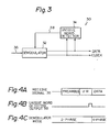
- FIG. 3 Another prior art system is shown in Fig. 3.
- the system generally 30, comprises a demodulator 32 and a unique word detector 34.
- a receive signal 36 which enters the system 30 has a format as shown in Fig. 4A.
- the output signal 38 of the unique word detector 34 is shown in Fig. 4B, and the operation modes of the demodulator 32 are shown in Fig. 4C. It will be seen that in this particular prior art system 30 on detection of a unique word the operation mode of the demodulator 32 is switched from a two-phase to a four-phase PSK mode.
- a transmit station when the operation mode is switched from one to another, a transmit station generates a plurality (K) of unique words after a unique word for synchronization, which is transmitted for each frame, and then modulates polarities of the K unique words to transmit K-bits binary data to thereby designate a modulation mode which is to hold next, while a receive station discriminates a switchover when more than a predetermined number of the unique words have been received within a predetermined period of time and identifies the modulation mode based on the K-bits binary data.
- K plurality
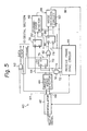
- a modulator/demodulator operation mode control system of the present invention is shown in Fig. 5 and signals appearing therein, in Figs. 6A-6F.
- the system generally 40, comprises a demodulator 42, a unique word detector 44, a receive frame synchronizing circuit 46, a switchover detector 48, a mode decision circuit 50, an AND gate 52, D-type flop-flops 54, 56 and 58, and Exclusive-OR gates 60 and 62.
- One output 64 of the demodulator 42 is applied to one input terminal of the unique word detector 44 and the Exclusive-OR gate 62, while the other output 66 is applied to the receive frame synchronizing circuit 46 and the other input terminal of the unique word detector 44.
- the demodulator output 66 is routed to a digital section as a clock.
- One output 68 of the unique word detector 44 is fed to the D flip-flop 56 and the AND gate 52, while the other output 70 is fed to the Exclusive-OR gate 60 and a D-terminal of the flip-flop 54.
- the output 72 of the AND gate 52 is coupled to the receive frame synchronizing circuit 46.
- One output 74 of the circuit 46 in turn is routed to the AND gate 52, a C-terminal of the D flip-flop 54, the mode decision circuit 50 and the switchover detector 48, while being delivered to the digital section as a frame output.
- the output of the D flip-flop 54 is applied to the Exclusive-OR gate 60 and the Exclusive-OR gate 62 which is adapted to apply data to the digital section.
- the other output 78 of the receive frame synchronizing circuit 46 is fed to the mode decision circuit 50, the D flip-flops 56 and 58, and the switchover detector 48.
- the output 80 of the Exclusive OR gate 60 is coupled to a D-terminal of the D flip-flop 58.
- the output 82 of the D flip-flop 56 is inputted to the mode decision circuit 50 as an output 84 of the switchover detector 48. Further, the output 86 of the D flip-flop 58 is fed back to the demodulator 42 by way of the mode decision circuit 50.
- a switchover signal is implemented with an F-bit signal which is a sequence of K unique words, each of which has L bits. It will be noted that if K.L ( F the switchover signal will be fully transmitted within one frame but, if otherwise, the switchover signal will occupy a plurality of frames.
- the system 40 shown in Fig. 5 is assumed to use a synchronous detection type demodulator.
- a "unique word for synchronization" 70 outputted by the unique word detector 44. i. e.
- unique word UW o is detected responsive to a "frame pulse" 74 which is outputted by the receive frame synchronizing circuit 46, thereby providing an "ambiguity remove signal” 76.
- the Exclusive-OR gate 60 to which the signal 76 is applied produces a unique pattern polarity signal 80 which is free from “ambiguity”.
- the signal 80 is discriminated responsive to an "aperture pulse” 78 and then applied to the mode decision circuit 50.
- a "unique word detection signal” (not dependent upon polarity) 68 is also discriminated responsive to an aperture pulse.. 78 and then fed to the switchover detector 48.
- the switchover detector 48 determines that a switchover signal frame has been received when, of the K unique words expected to arrive in the case of a switchover signal, more than a predetermined number (e. g. T) of unique words have occurred.
- the mode decision circuit 50 decodes a mode instruction signal and then generates a "demodulator mode control signal" 88 to start controlling the demodulator 42 in a new mode at a predetermined timing.
- the system 40 having the above construction will be operated as follows.
- a transmit station When changing the operation mode is decided, a transmit station subjects a plurality (K) of unique words UW, UW,, UW 2 , ..., UW x , which are to be transmitted after a synchronizing unique word (UW o in this particular embodiment) that appears for each frame, to "polarity modulation" in order to send K-bit binary data which designates a modulation mode to hold next. Simultaneously, the transmit station switches over the transmission mode at the beginning of the next frame or at any other predetermined timing.
- K synchronizing unique word
- a receive station samples and stores presence of unique words as well as polarity detection signals responsive to a timing signal, which is supplied thereto from the receive frame synchronizing circuit 46.
- the receive station determines that a switchover signal has been received, then decodes the binary code as represented by the stored polarity detection signals to thereby select an operation mode of the demodulator 42 which is to hold next, and then switches the demodulator mode at the beginning of the next frame or at any other predetermined timing.
- the system 40 is capable of surely changing the operation mode even when the SN ratio is poor. Specifically, concerning the detection of a unique word itself (assumed to have a length of L bits) , there are provided L bits which is long enough to be detected even under poor SN ratio conditions, a word having high self-correlation, and an allowable number of error bits (with a threshold value A), so that the unique word detection error rate is sufficiently lower than the bit error rate. Even though the number of bit errors in the unique word may exceed the threshold value to such an extent that a unique word is overlooked, the probability of failing to correctly decide polarity (decision by majority of L/2) is negligible.
- the sampling which uses aperture pulses as previously stated is effective to substantially exclude erroneous detection pulses which may appear even during steady operation due to accidental coincidence between an L-bit signal included in random transmit - signals and the unique word.
- the code length K which is an important constant in switchover detection and an allowable number of overlooks, it is possible to suppress the probability of malfunction of the system due to detection error to a practically negligible degree.
- a modulator/demodulator furnished with numerous operation modes is surely operable even under poor SN ratio conditions without the need for order wires and whenever desired and in any desired mode.
- This offers users who use various different signal modes high-speed and highly reliable signal transmission services by setting up an optimum operation mode, i. e.. a combination of data rate, modulation system, error-correcting coding rate and others which is most effective for given transmission conditions.
- the present invention allows a versatile, flexible and high-performance satellite communication link to be set up which is extensively applicable to bussines3 communication and mobile communication.
Abstract
Description
- The present invention relates to a system for controlling operation mode of a modulator/demodulator which is applicable to satellite communication. More particularly, the present invention is concerned with an operation mode control system for a modulator/demodulator useful for business communication and mobile communication of the kind using high frequency bands such as a Ku band, which is a promising high frequency band.
- Satellite communication, compared to ground communication, requires a modulator/demodulator which is operable under lower signal-to-noise (SN) ratio conditions because it cannot avoid attenuation due to far longer transmission links. Especially, a demodulator for phase modulation adapted for synchronous detection has to positively tune a carrier recovery circuit at a sufficiently high SN ratio. One approach known in the art to meet this requirement is using a modulator switchover system which causes a modulator to perform two-phase PSK (phase shift keying) demodulation for a preamble signal and four-phase PSK demodulation for a transmit signal. Such a switchable demodulator scheme is disclosed in. for example, Japanese Patent Publication Nos. 53-23649 (U. S. Patent No. 3,815,034) and 58-55709 which respectively are entitled "Phase-Modulated Wave Demodulator" and "Phase Demodulator".
- The prior art systems will be described with reference to the accompanying drawings. In Fig. 1, a prior art system is shown and generally designated by the
reference numeral 10. Thesystem 10 comprises ademodulator 12, anenvelope detector 14, athreshold detector 16, and atimer 18. Areceive signal 20 which is applied to thesystem 10 has a format as shown in Fig. 2A. Output signals 22, 24 and 26 of theenvelope detector 14,threshold detector 16 andtimer 18, respectively, have waveforms as shown in Figs. 2B, 2C and 2D. Thedemodulator 12 is selectively operable in different modes as shown in Fig. 2E. As shown in Figs. 2A-2E, when arrival of a signal has been detected in a no-signal condition, thedemodulator 12 is caused to operate in a two-phase PSK mode and then in a four-phase PSK mode. Another prior art system is shown in Fig. 3. In Fig. 3 the system, generally 30, comprises ademodulator 32 and aunique word detector 34. A receivesignal 36 which enters thesystem 30 has a format as shown in Fig. 4A. Theoutput signal 38 of theunique word detector 34 is shown in Fig. 4B, and the operation modes of thedemodulator 32 are shown in Fig. 4C. It will be seen that in this particularprior art system 30 on detection of a unique word the operation mode of thedemodulator 32 is switched from a two-phase to a four-phase PSK mode. - The problem with the
prior art system 10 of Figs. 1 and 2A-2E, which detects an envelope and then a threshold value, is that it is liable to perform faulty detection under low SN ratio conditions. Meanwhile, theprior art system 30 of Figs. 3 and 4A-4E has the drawback that if it overlooks a unique word even once, the communication is practically disenabled from the start. - While any of the prior art systems discussed above allows the demodulator to operate in a two-phase PSK mode during an initial stage of operation and a four-phase mode during a steady communication stage, communication of the kind keenly demanded today for business transactions uses a modulator/demodulator which is operable in a far greater number of operation modes. For example, the following factors are used in various combinations:
-

- It is remarkably effective to combine various modes as stated above so that one may hold a communication with an optimum modulation system selected on the basis of user's signal conditions (voice, data), SN ratio of the transmission path (attenuation due to rain, etc. ) , frequency band in use (Ku band, C band, etc.), and others. Although such may be implemented utilizing order wires of a TDMA (time division multiple access) communication system, installing order wires in business communication, mobile communication and others which involve numerous users is undesirable because the order wires would reduce the system capacity available for communication. Moreover, any of the prior art systems shown and described is incapable of controlling a modulator/demodulator having a great number of different operation modes as previously mentioned.
- It is therefore an object of the present invention to provide a modulator/demodulator operation mode control system which is capable of controlling a modulator/demodulator having numerous operation modes.
- It is another object of the present invention to provide a modulator/demodulator operation mode control system which eliminates the need for order wires otherwise required for control, surely operates even in a low SN ratio condition, and adapts itself to both synchronous detection and asynchronous detection.
- It is another object of the present invention to provide a system for controlling operation mode of a modulator/demodulator.
- In accordance with the present invention, in a system for controlling operation mode of a modulator/demodulator which switches over operation mode of the modulator/demodulator responsive to a particular combination of modulation system, error-correction coding system and data transmission rate, when the operation mode is switched from one to another, a transmit station generates a plurality (K) of unique words after a unique word for synchronization, which is transmitted for each frame, and then modulates polarities of the K unique words to transmit K-bits binary data to thereby designate a modulation mode which is to hold next, while a receive station discriminates a switchover when more than a predetermined number of the unique words have been received within a predetermined period of time and identifies the modulation mode based on the K-bits binary data.
- The above and other objects, features and advantages of the present invention will become more apparent from the following detailed description taken with the accompanying drawings.
-
- Fig. 1 is a block diagram showing an example of prior art systems for controlling operation mode of a modulator/demodulator;
- Figs. 2A-2E show waveforms representative of operation of the system shown in Fig. 1;
- Fig. 3 is a block diagram showing another example of the prior art systems;
- Figs. 4A-4C show waveforms representative of operation of the system shown in Fig. 3;
- Fig. 5 is a block diagram showing a modulator/demodulator operation mode control system embodying the present invention; and
- Fig. 6 shows waveforms demonstrating operation of the system of Fig. 5.
- While the system for controlling operation mode of a modulator/demodulator of the present invention is susceptible of numerous physical embodiments, depending upon the environment and requirements of use, a substantial number of the herein shown and described embodiment have been made, tested and used, and all have performed in an eminently satisfactory manner.
- A modulator/demodulator operation mode control system of the present invention is shown in Fig. 5 and signals appearing therein, in Figs. 6A-6F.
- Referring to Fig. 5, the system, generally 40, comprises a
demodulator 42, aunique word detector 44, a receiveframe synchronizing circuit 46, aswitchover detector 48, amode decision circuit 50, anAND gate 52, D-type flop-flops OR gates output 64 of thedemodulator 42 is applied to one input terminal of theunique word detector 44 and the Exclusive-ORgate 62, while theother output 66 is applied to the receiveframe synchronizing circuit 46 and the other input terminal of theunique word detector 44. At the same time, thedemodulator output 66 is routed to a digital section as a clock. Oneoutput 68 of theunique word detector 44 is fed to the D flip-flop 56 and theAND gate 52, while theother output 70 is fed to the Exclusive-ORgate 60 and a D-terminal of the flip-flop 54. Theoutput 72 of theAND gate 52 is coupled to the receiveframe synchronizing circuit 46. Oneoutput 74 of thecircuit 46 in turn is routed to theAND gate 52, a C-terminal of the D flip-flop 54, themode decision circuit 50 and theswitchover detector 48, while being delivered to the digital section as a frame output. The output of the D flip-flop 54 is applied to the Exclusive-ORgate 60 and the Exclusive-ORgate 62 which is adapted to apply data to the digital section. Theother output 78 of the receiveframe synchronizing circuit 46 is fed to themode decision circuit 50, the D flip-flops switchover detector 48. Theoutput 80 of the Exclusive ORgate 60 is coupled to a D-terminal of the D flip-flop 58. Theoutput 82 of the D flip-flop 56 is inputted to themode decision circuit 50 as anoutput 84 of theswitchover detector 48. Further, theoutput 86 of the D flip-flop 58 is fed back to thedemodulator 42 by way of themode decision circuit 50. - As shown in Figs. 6A and 6B, in accordance with the illustrative embodiment, a switchover signal is implemented with an F-bit signal which is a sequence of K unique words, each of which has L bits. It will be noted that if K.L ( F the switchover signal will be fully transmitted within one frame but, if otherwise, the switchover signal will occupy a plurality of frames. The
system 40 shown in Fig. 5 is assumed to use a synchronous detection type demodulator. A "unique word for synchronization" 70 outputted by theunique word detector 44. i. e. , unique word UWo is detected responsive to a "frame pulse" 74 which is outputted by the receiveframe synchronizing circuit 46, thereby providing an "ambiguity remove signal" 76. The Exclusive-OR gate 60 to which thesignal 76 is applied produces a uniquepattern polarity signal 80 which is free from "ambiguity". Thesignal 80 is discriminated responsive to an "aperture pulse" 78 and then applied to themode decision circuit 50. Meanwhile, a "unique word detection signal" (not dependent upon polarity) 68 is also discriminated responsive to an aperture pulse.. 78 and then fed to theswitchover detector 48. Theswitchover detector 48 determines that a switchover signal frame has been received when, of the K unique words expected to arrive in the case of a switchover signal, more than a predetermined number (e. g. T) of unique words have occurred. On detection of a switchover signal, themode decision circuit 50 decodes a mode instruction signal and then generates a "demodulator mode control signal" 88 to start controlling thedemodulator 42 in a new mode at a predetermined timing. - The
system 40 having the above construction will be operated as follows. - When changing the operation mode is decided, a transmit station subjects a plurality (K) of unique words UW, UW,, UW2, ..., UWx, which are to be transmitted after a synchronizing unique word (UWo in this particular embodiment) that appears for each frame, to "polarity modulation" in order to send K-bit binary data which designates a modulation mode to hold next. Simultaneously, the transmit station switches over the transmission mode at the beginning of the next frame or at any other predetermined timing.
- A receive station, on the other hand, samples and stores presence of unique words as well as polarity detection signals responsive to a timing signal, which is supplied thereto from the receive
frame synchronizing circuit 46. When the receive station has detected more than a predetermined number of unique words within a predetermined period of time, it determines that a switchover signal has been received, then decodes the binary code as represented by the stored polarity detection signals to thereby select an operation mode of thedemodulator 42 which is to hold next, and then switches the demodulator mode at the beginning of the next frame or at any other predetermined timing. - As described above, the
system 40 is capable of surely changing the operation mode even when the SN ratio is poor. Specifically, concerning the detection of a unique word itself (assumed to have a length of L bits) , there are provided L bits which is long enough to be detected even under poor SN ratio conditions, a word having high self-correlation, and an allowable number of error bits (with a threshold value A), so that the unique word detection error rate is sufficiently lower than the bit error rate. Even though the number of bit errors in the unique word may exceed the threshold value to such an extent that a unique word is overlooked, the probability of failing to correctly decide polarity (decision by majority of L/2) is negligible. - The sampling which uses aperture pulses as previously stated is effective to substantially exclude erroneous detection pulses which may appear even during steady operation due to accidental coincidence between an L-bit signal included in random transmit - signals and the unique word. By adequately selecting the code length K which is an important constant in switchover detection and an allowable number of overlooks, it is possible to suppress the probability of malfunction of the system due to detection error to a practically negligible degree.
- In accordance with the present invention, a modulator/demodulator furnished with numerous operation modes is surely operable even under poor SN ratio conditions without the need for order wires and whenever desired and in any desired mode. This offers users who use various different signal modes high-speed and highly reliable signal transmission services by setting up an optimum operation mode, i. e.. a combination of data rate, modulation system, error-correcting coding rate and others which is most effective for given transmission conditions. The present invention allows a versatile, flexible and high-performance satellite communication link to be set up which is extensively applicable to bussines3 communication and mobile communication.
- Various modifications will become possible for those skilled in the art after receiving the teachings of the present disclosure without departing from the scope thereof.
Claims (1)
Applications Claiming Priority (2)
| Application Number | Priority Date | Filing Date | Title |
|---|---|---|---|
| JP75131/85 | 1985-04-09 | ||
| JP60075131A JPH0654923B2 (en) | 1985-04-09 | 1985-04-09 | Mode of operation control of modulator / demodulator |
Publications (3)
| Publication Number | Publication Date |
|---|---|
| EP0197541A2 true EP0197541A2 (en) | 1986-10-15 |
| EP0197541A3 EP0197541A3 (en) | 1988-09-21 |
| EP0197541B1 EP0197541B1 (en) | 1992-01-22 |
Family
ID=13567330
Family Applications (1)
| Application Number | Title | Priority Date | Filing Date |
|---|---|---|---|
| EP86104775A Expired - Lifetime EP0197541B1 (en) | 1985-04-09 | 1986-04-08 | System for controlling operation mode of modulator/demodulator |
Country Status (6)
| Country | Link |
|---|---|
| US (1) | US4833696A (en) |
| EP (1) | EP0197541B1 (en) |
| JP (1) | JPH0654923B2 (en) |
| AU (1) | AU586858B2 (en) |
| CA (1) | CA1267703A (en) |
| DE (1) | DE3683522D1 (en) |
Cited By (3)
| Publication number | Priority date | Publication date | Assignee | Title |
|---|---|---|---|---|
| GB2210237A (en) * | 1987-09-18 | 1989-06-01 | Racal Data Communications Inc | Constellation multiplexed inband secondary channel for voiceband modem |
| US4852122A (en) * | 1987-08-31 | 1989-07-25 | Universal Data Systems, Inc. | Modem suited for wireless communication channel use |
| WO2014141042A1 (en) | 2013-03-11 | 2014-09-18 | N.G.M. Sprl | Tricycle |
Families Citing this family (15)
| Publication number | Priority date | Publication date | Assignee | Title |
|---|---|---|---|---|
| US5054034A (en) * | 1985-05-20 | 1991-10-01 | Telebit Corporation | Ensemble modem structure for imperfect transmission media |
| JPH0817428B2 (en) * | 1988-11-22 | 1996-02-21 | 株式会社日立製作所 | Modulator / demodulator |
| EP0385042A1 (en) * | 1989-02-28 | 1990-09-05 | International Business Machines Corporation | Method of adjusting the end of transmission in a modem |
| EP0389165B1 (en) * | 1989-03-21 | 1996-06-12 | Minnesota Mining And Manufacturing Company | Fiber optic data link system |
| JP3077881B2 (en) * | 1995-03-07 | 2000-08-21 | 日本電気株式会社 | Demodulation method and demodulation device |
| US5974106A (en) * | 1995-09-01 | 1999-10-26 | Motorola, Inc. | Method and apparatus for multirate data communications |
| US6068933A (en) | 1996-02-15 | 2000-05-30 | American National Can Company | Thermoformable multilayer polymeric film |
| JPH10322407A (en) * | 1997-05-16 | 1998-12-04 | Matsushita Electric Ind Co Ltd | Dual band data communication equipment |
| US6381250B1 (en) | 1998-01-23 | 2002-04-30 | Innovative Communications Technologies, Inc. | Capacity allocation system using semi-autonomous network elements to implement and control a transmission schedule |
| US6426959B1 (en) | 1998-01-20 | 2002-07-30 | Innovative Communications Technologies, Inc. | System and method for facilitating component management in a multiple vendor satellite communications network |
| US6567475B1 (en) * | 1998-12-29 | 2003-05-20 | Ericsson Inc. | Method and system for the transmission, reception and processing of 4-level and 8-level signaling symbols |
| IL130540A (en) * | 1999-06-17 | 2003-07-31 | Tadiran Telecom Business Syste | System having a port with two operating modes |
| JP4517430B2 (en) * | 2000-01-24 | 2010-08-04 | ソニー株式会社 | Wireless transmission method |
| US8106813B2 (en) * | 2010-01-27 | 2012-01-31 | Unnikrishna Sreedharan Pillai | Multichannel constant envelope orthogonal waveforms using receiver design |
| JP5877388B2 (en) | 2010-12-20 | 2016-03-08 | パナソニックIpマネジメント株式会社 | COMMUNICATION DEVICE, COMMUNICATION METHOD, TERMINAL DEVICE, AND COMMUNICATION SYSTEM |
Citations (1)
| Publication number | Priority date | Publication date | Assignee | Title |
|---|---|---|---|---|
| EP0154565A2 (en) * | 1984-03-08 | 1985-09-11 | Codex Corporation | Modem |
Family Cites Families (11)
| Publication number | Priority date | Publication date | Assignee | Title |
|---|---|---|---|---|
| US3688197A (en) * | 1965-10-21 | 1972-08-29 | Kahn Res Lab | Communication system with selection means for determining the modulation mode of a received signal |
| JPS49131610A (en) * | 1973-04-22 | 1974-12-17 | ||
| US4055808A (en) * | 1976-05-20 | 1977-10-25 | Intertel, Inc. | Data communications network testing system |
| US4128809A (en) * | 1976-08-31 | 1978-12-05 | Nippon Electric Co., Ltd. | Time diversity receiver for processing repeatedly received signal bits in consideration of a maximum-level and/or a favorably received signal bit |
| DE2641782A1 (en) * | 1976-09-17 | 1978-03-23 | Licentia Gmbh | CIRCUIT ARRANGEMENT FOR THE DIGITAL FREQUENCY DISPLAY OF THE AM AND FM RANGE IN A BROADCASTING DEVICE |
| US4156867A (en) * | 1977-09-06 | 1979-05-29 | Motorola, Inc. | Data communication system with random and burst error protection and correction |
| US4387440A (en) * | 1980-03-03 | 1983-06-07 | Eaton Michael D | Modem control device code multiplexing |
| FR2503965B1 (en) * | 1981-04-08 | 1987-07-24 | Thomson Csf | METHOD FOR PROTECTION AGAINST TRANSMISSION ERRORS OF RADIO-TELEGRAPHIC MESSAGES AND DEVICE FOR IMPLEMENTING SAME |
| US4549302A (en) * | 1981-06-15 | 1985-10-22 | Hayes Microcomputer Products, Inc. | Modem with improved escape sequence mechanism to prevent escape in response to random occurrence of escape character in transmitted data |
| US4481489A (en) * | 1981-07-02 | 1984-11-06 | Motorola Inc. | Binary signal modulating circuitry for frequency modulated transmitters |
| US4620294A (en) * | 1983-09-09 | 1986-10-28 | Cts Corporation | Digital signal processor modem |
-
1985
- 1985-04-09 JP JP60075131A patent/JPH0654923B2/en not_active Expired - Lifetime
-
1986
- 1986-04-02 US US06/847,366 patent/US4833696A/en not_active Expired - Fee Related
- 1986-04-07 AU AU55697/86A patent/AU586858B2/en not_active Ceased
- 1986-04-08 EP EP86104775A patent/EP0197541B1/en not_active Expired - Lifetime
- 1986-04-08 DE DE8686104775T patent/DE3683522D1/en not_active Expired - Fee Related
- 1986-04-08 CA CA000506054A patent/CA1267703A/en not_active Expired - Fee Related
Patent Citations (1)
| Publication number | Priority date | Publication date | Assignee | Title |
|---|---|---|---|---|
| EP0154565A2 (en) * | 1984-03-08 | 1985-09-11 | Codex Corporation | Modem |
Non-Patent Citations (2)
| Title |
|---|
| DEUXIEME COLLOQUE INTERNATIONAL SUR LES TELECOMMUNICATIONS NUMERIQUES PAR SATELLITE, 28th-30th November 1972, Paris, pages 256 - 265, Ed. Chiron, Paris, FR; A. OGAWA et al.: 'A new eight-phase PSK modem system for TDMA' * |
| IEEE TRANSACTIONS ON COMMUNICATION TECHNOLOGY, vol. COM-16, no. 4, August 1968, pages 597 - 605, IEEE, New York, US; W. SCHREMPP et al.: 'Unique word detection in digital burst communications' * |
Cited By (6)
| Publication number | Priority date | Publication date | Assignee | Title |
|---|---|---|---|---|
| US4852122A (en) * | 1987-08-31 | 1989-07-25 | Universal Data Systems, Inc. | Modem suited for wireless communication channel use |
| GB2210237A (en) * | 1987-09-18 | 1989-06-01 | Racal Data Communications Inc | Constellation multiplexed inband secondary channel for voiceband modem |
| GB2245457A (en) * | 1987-09-18 | 1992-01-02 | Racal Data Communications Inc | Data modem synchronisation |
| GB2245457B (en) * | 1987-09-18 | 1992-04-01 | Racal Data Communications Inc | Modem synchronization |
| GB2210237B (en) * | 1987-09-18 | 1992-04-01 | Racal Data Communications Inc | Constellation multiplexed inband secondary channel for voiceband modem |
| WO2014141042A1 (en) | 2013-03-11 | 2014-09-18 | N.G.M. Sprl | Tricycle |
Also Published As
| Publication number | Publication date |
|---|---|
| EP0197541A3 (en) | 1988-09-21 |
| CA1267703A (en) | 1990-04-10 |
| US4833696A (en) | 1989-05-23 |
| JPS61234154A (en) | 1986-10-18 |
| AU586858B2 (en) | 1989-07-27 |
| EP0197541B1 (en) | 1992-01-22 |
| JPH0654923B2 (en) | 1994-07-20 |
| DE3683522D1 (en) | 1992-03-05 |
| AU5569786A (en) | 1986-10-16 |
Similar Documents
| Publication | Publication Date | Title |
|---|---|---|
| EP0197541A2 (en) | System for controlling operation mode of modulator/demodulator | |
| US5023889A (en) | Trellis coded multilevel DPSK system with doppler correction for mobile satellite channels | |
| AU672700B2 (en) | Method and apparatus for establishing and maintaining frame synchronization in a satellite communication system | |
| US4099121A (en) | Spatial diversity satellite communications system with error control | |
| US4639937A (en) | HF avalanche relay communication technique | |
| US4107608A (en) | Method and apparatus for burst synchronization in a time division multiple access communication system | |
| US4105973A (en) | Multibeam, digitally modulated, time division, switched satellite communications system | |
| KR20000005381A (en) | Improved technique for jointly performing bit synchronization and error detection in a tdm/tdma system | |
| US4527279A (en) | Synchronization circuit for a Viterbi decoder | |
| EP0025217A1 (en) | Clock recovery circuit for burst communications systems | |
| KR100671508B1 (en) | Signalling method and telecommunication system | |
| US4663768A (en) | Diversity system of selection type equipped with a code correction/switch circuit for receiving a PSK or QAM wave carrying differentially encoded signal | |
| GB2334856A (en) | Diversity reception antenna switching based on phase error detection | |
| US5515380A (en) | Reducing errors in digital communication | |
| US5285458A (en) | System for suppressing spread of error generated in differential coding | |
| US5654989A (en) | Method and apparatus for symbol timing tracking | |
| US7242696B2 (en) | Digital TDMA link with no sync word | |
| US7095818B2 (en) | Data transmission process with auto-synchronized correcting code, auto-synchronized coder and decoder, corresponding transmitter and receiver | |
| EP0886393B1 (en) | TDMA voice information reading apparatus | |
| Chang et al. | Performance of a TDMA portable radio system using a block code for burst synchronization and error detection | |
| JPH0225306B2 (en) | ||
| AU744820B2 (en) | A circuit and method for receiving data | |
| JPS6346616B2 (en) | ||
| Ryan | Optimal signaling for meteor burst channels | |
| US4426711A (en) | Process for the transmission of service signals for a digital radio beam, as well as transmitter and receiver for using such a process |
Legal Events
| Date | Code | Title | Description |
|---|---|---|---|
| PUAI | Public reference made under article 153(3) epc to a published international application that has entered the european phase |
Free format text: ORIGINAL CODE: 0009012 |
|
| 17P | Request for examination filed |
Effective date: 19860408 |
|
| AK | Designated contracting states |
Kind code of ref document: A2 Designated state(s): DE FR GB NL |
|
| PUAL | Search report despatched |
Free format text: ORIGINAL CODE: 0009013 |
|
| AK | Designated contracting states |
Kind code of ref document: A3 Designated state(s): DE FR GB NL |
|
| 17Q | First examination report despatched |
Effective date: 19900808 |
|
| GRAA | (expected) grant |
Free format text: ORIGINAL CODE: 0009210 |
|
| AK | Designated contracting states |
Kind code of ref document: B1 Designated state(s): DE FR GB NL |
|
| REF | Corresponds to: |
Ref document number: 3683522 Country of ref document: DE Date of ref document: 19920305 |
|
| ET | Fr: translation filed | ||
| PLBE | No opposition filed within time limit |
Free format text: ORIGINAL CODE: 0009261 |
|
| STAA | Information on the status of an ep patent application or granted ep patent |
Free format text: STATUS: NO OPPOSITION FILED WITHIN TIME LIMIT |
|
| 26N | No opposition filed | ||
| PGFP | Annual fee paid to national office [announced via postgrant information from national office to epo] |
Ref country code: GB Payment date: 19960403 Year of fee payment: 11 |
|
| PGFP | Annual fee paid to national office [announced via postgrant information from national office to epo] |
Ref country code: FR Payment date: 19960423 Year of fee payment: 11 |
|
| PGFP | Annual fee paid to national office [announced via postgrant information from national office to epo] |
Ref country code: NL Payment date: 19960430 Year of fee payment: 11 |
|
| PGFP | Annual fee paid to national office [announced via postgrant information from national office to epo] |
Ref country code: DE Payment date: 19960627 Year of fee payment: 11 |
|
| PG25 | Lapsed in a contracting state [announced via postgrant information from national office to epo] |
Ref country code: GB Effective date: 19970408 |
|
| PG25 | Lapsed in a contracting state [announced via postgrant information from national office to epo] |
Ref country code: NL Effective date: 19971101 |
|
| GBPC | Gb: european patent ceased through non-payment of renewal fee |
Effective date: 19970408 |
|
| PG25 | Lapsed in a contracting state [announced via postgrant information from national office to epo] |
Ref country code: FR Free format text: LAPSE BECAUSE OF NON-PAYMENT OF DUE FEES Effective date: 19971231 |
|
| PG25 | Lapsed in a contracting state [announced via postgrant information from national office to epo] |
Ref country code: DE Free format text: LAPSE BECAUSE OF NON-PAYMENT OF DUE FEES Effective date: 19980101 |
|
| NLV4 | Nl: lapsed or anulled due to non-payment of the annual fee |
Effective date: 19971101 |
|
| REG | Reference to a national code |
Ref country code: FR Ref legal event code: ST |