EP0205009B1 - System for encoding a data stream into a run length limited symbol string - Google Patents
System for encoding a data stream into a run length limited symbol string Download PDFInfo
- Publication number
- EP0205009B1 EP0205009B1 EP86107017A EP86107017A EP0205009B1 EP 0205009 B1 EP0205009 B1 EP 0205009B1 EP 86107017 A EP86107017 A EP 86107017A EP 86107017 A EP86107017 A EP 86107017A EP 0205009 B1 EP0205009 B1 EP 0205009B1
- Authority
- EP
- European Patent Office
- Prior art keywords
- rll
- byte
- symbol
- parallel
- sequence
- Prior art date
- Legal status (The legal status is an assumption and is not a legal conclusion. Google has not performed a legal analysis and makes no representation as to the accuracy of the status listed.)
- Expired
Links
Images


Classifications
-
- G—PHYSICS
- G06—COMPUTING; CALCULATING OR COUNTING
- G06T—IMAGE DATA PROCESSING OR GENERATION, IN GENERAL
- G06T9/00—Image coding
- G06T9/005—Statistical coding, e.g. Huffman, run length coding
-
- H—ELECTRICITY
- H03—ELECTRONIC CIRCUITRY
- H03M—CODING; DECODING; CODE CONVERSION IN GENERAL
- H03M5/00—Conversion of the form of the representation of individual digits
- H03M5/02—Conversion to or from representation by pulses
- H03M5/04—Conversion to or from representation by pulses the pulses having two levels
- H03M5/14—Code representation, e.g. transition, for a given bit cell depending on the information in one or more adjacent bit cells, e.g. delay modulation code, double density code
- H03M5/145—Conversion to or from block codes or representations thereof
Definitions
- This invention relates to a system for encoding an input byte-wide data stream into an output run-lenth-limited (RLL) symbol string or for decoding an output byte-wide data stream from an input RLL symbol string.
- RLL run-lenth-limited
- RLL run-length-limited
- the (1,7) format is gaining increasing acceptance in the industry as the preferred RLL coding format for present magnetic disk technology.
- the RLL (1,7) coding format a sequence of unencoded binary data is converted into an encoded bit string in which each one in a coded bit sequence must be separated from the nearest adjacent one by at least one, but no more than seven zeros.
- the most efficient coding rate results when every two unencoded data bits are converted into three coded bits.
- three coded data bits are converted into two decoded data bits.
- FIG. 1 A typical prior art architecture employing RLL (1,7) coding in a magnetic disk storage system is illustrated in Figure 1.
- unencoded data from a data processing system is provided to the encoder section of an encoder/decoder (ENC/DEC) through a serializer/deserializer (S/D).
- S/D serializer/deserializer
- the data is normally in parallel byte form, which must be serialized into a sequence of 2-bit groups.
- Each 2-bit group provided to the encoder results in the provision of three encoded bits that go to a buffer (B) for serialization into an encoded, bit-wide data string that is processed by drive circuitry for writing onto a magnetic disk. In the industry, this is referred to as bit-by-bit encoding.
- bit-wide encoded data string is provided through the buffer B in the form of successive groups of three encoded bits to the decoder section of the encoder/decoder. Each successive group of three encoded bits is decoded to a group of two data bits (bit-by-bit decoding).
- the succession of bit pairs from the decoder are converted by the serializer/deserializer into a succession of bytes that are forwarded to the data processing system.
- An artifact of the bit-by-bit coding system of Figure 1 is the requirement for at least two conversion clocks: an f C clock for the encoded bit channel and a 2/3 f C clock for the transfer of data between the serializer/deserializer S/D and the buffer B.
- the f C clock can be derived conventionally from a disk servo clock while writing information to a disk or from encoded read data obtained from a disk while reading information from the disk. Normally, f C is obtained under either circumstance through a voltage-frequency oscillator (VFO).
- VFO voltage-frequency oscillator
- the 2/3 f C clock is usually derived by use of a second VFO synchronized to the f C clock. This imposes an added hardware requirement and requires the settling times of two VFO's to be accounted for when the timing source to the f C VFO is switched.
- Figure 1 architecture requires an extra format conversion for unencoded and decoded data passing between the serializer/deserializer and encoder/decoder, further adding complexity to the system.
- the typical prior art RLL (1,7) encoder consists of a finite-state machine whose internal state is described by three state bits. Plural state bits increase the logic and storage hardware requirements of the encoder, which make it awkward for being cascaded in parallel to provide byte-wide encoding.
- the technical problem that is solved by the system of the invention is the elimination of the need for an odd 2/3 f C clock to shift unencoded or decoded data relative to the bit rate of the encoded channel.
- the invention is based upon the simultaneous coding conversion of an entire byte of data, which permits the system to transfer decoded or unencoded data at the byte rate and eliminates the requirement for the odd 2/3 rate clock.
- the system is one for encoding an input byte-wide data sequence into an output run-length-limited (RLL) symbol string and for decoding an output byte-wide data sequence from an input RLL symbol string.
- RLL run-length-limited
- the system includes an RLL encoder that responds to consecutive parallel unencoded bytes occurring at a byte rate in an input byte-wide data sequence by producing an output RLL symbol sequence including consecutive groups of parallel RLL symbols.
- a format converter is connected to the RLL encoder for converting the output RLL symbol sequence into an output RLL-encoded symbol string having a symbol string rate which is a whole multiple of the byte rate.
- the format converter further responds to an input RLL symbol string having an input symbol string rate, by providing an input RLL symbol sequence including consecutive groups of parallel RLL symbols.
- An RLL decoder responds to the input RLL symbol sequence constructed by the format converter by producing, at the byte rate, an output byte-wide data sequence including consecutive parallel bytes of decoded data.
- the primary objective of the system is to provide a bi-directional code conversion interface between a channel conducting a sequence of consecutive parallel bytes of data at a byte rate and a data channel conducting strings of RLL (1,7) symbols at a symbol string rate.
- An advantage of the present invention is the elimination of the need for an odd clock signal having 2/3 the frequency of the symbol channel.
- FIG. 1 is a block diagram of code conversion architecture in the prior art.
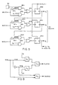
- FIG. 2 is a block diagram illustrating the general architecture of the system of the invention.
- FIG. 3 is a more detailed illustration of the functional blocks included in the system of the invention.
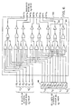
- Figure 4 is a waveform diagram illustrating read and write modes of operation of the system of the invention.
- Figure 5 is a schematic diagram illustrating a format converter used in the system of the invention.
- Figure 6 is a schematic diagram illustrating a decoder for converting twelve bits of RLL (1,7)-encoded data simultaneously into a parallel byte of decoded data.
- Figure 7 is a circuit diagram of the encoder used to simultaneously encode a byte of unencoded data into twelve bits of RLL (1,7)-encoded data.
- Figure 8 is a gating circuit used to steer byte clock signals during read and write operations of the invention.
- a byte of data is taken, as in the usual sense, to denote a sequence of eight adjacent binary digits (bits) that are operated upon as a unit.
- a parallel byte refers to the eight bits transferred simultaneously on a data channel including 8 parallel transmission paths.
- a string refers to a linear sequence of bits.
- a coded symbol consists of a group of three consecutive bits resulting from an encoding operation performed on two bits of unencoded data.
- a symbol string is a string of encoded bits in which successive groups of three bits form successive symbols.
- weight is assigned a bit in a data string according to its place in the string.
- the first bit is accorded the most significance (MSB) and is assigned the lowest-numerical subscript, e.g., x0. Bits occurring after the MSB have correspondingly less significance, but subscripts of higher magnitude.
- MSB most significance
- bit x0 the first bit
- bit x7 the last bit
- this significance convention is observed for unencoded bits (x), encoded bits (y), and symbols(Y).
- the system of the invention accepts an input byte sequence constituting a succession of parallel bytes on a data channel that is eight bits wide. Each byte consists of eight simultaneously-transferred bits.
- the byte sequence is fed to the system 10 for being encoded into an output consisting of a string of RLL (1,7)-encoded symbols.
- An input byte sequence can be provided from a conventional data processing system (not shown) for being entered (written) onto a magnetic disk (also not shown) for storage and later retrieval.
- the input byte sequence is converted by the system of the invention to an output symbol string, in which form it is stored on the disk.
- an input symbol string is obtained from the disk and provided to the system 10 for conversion into a decoded output byte sequence that is forwarded to the data processing system.
- the system 10 operates in conjunction with conventional disk control logic 12 that provides a read/write (R/W) gate signal for defining the mode of operation for the system 10.
- R/W read/write
- the control logic includes a VFO (not shown) to generate a symbol channel clock f C and a multi-phase byte clock f B that is constrained to be an integer sub-multiple of f C .
- the control logic 12 also provides conventional signals MUX 1 and MUX 2 for controlling conventional multiplexing and format conversion circuitry in the system 10.
- the system 10 is a byte-wide encoder and decoder for RLL (1,7) code and includes an RLL encoder 16 that accepts consecutive bytes of an input byte sequence at a byte rate f B and encodes them according to RLL (1,7) coding rules into a write symbol group sequence (WSGS).
- the write symbol group sequence consists of a sequence of groups of parallel encoded symbol bits.
- the 2/3 conversion rate constrains each group of the write symbol group sequence to twelve bits, which form 4 symbols.
- the write symbol group sequence is provided to a serializer/deserializer circuit 18 that, during a write mode of operation, performs parallel-to-serial format conversion to convert the 12-bit wide write symbol group sequence into a bit-wide output symbol string having a string rate f C that is equal to 12 f B .
- the serializer/deserializer circuit 18 receives a bit-wide input symbol string at the string rate f C and performs serial-to-parallel format conversion on the input string to produce a read symbol group sequence (RSGS) consisting of the succession of groups of twelve parallel encoded data bits.
- the read symbol group sequence is provided to an RLL decoder 20 which converts the sequence to a corresponding parallel byte sequence of decoded bits that is forwarded at the byte rate f B to the data processing system as read data.
- the system 10 preferably operates in a conventional magnetic disk storage unit for encoding a parallel byte sequence of data to be written to a magnetic disk.
- the parallel byte stream is provided as write data from a data processing system (not shown) and is delivered unencoded to the system 10.
- the write data is converted by the system of the invention to an RLL (1,7)-encoded bit string comprising symbol channel write data which is submitted to disk drive electronics (not shown) for being entered on a magnetic disk (also not shown).
- This mode of operation is referred to hereinbelow as the WRITE mode and is signified by a WRITE state of the R/W signal produced by the control logic 12.
- an RLL (1,7)-encoded bit string comprising symbol channel read data obtained from the disk drive electronics for delivery to the data processing system is delivered to the system 10 for conversion to a decoded parallel byte sequence which is transferred by conventional means to the data processing system.
- the byte-wide encoder and decoder system for RLL (1,7) code pictured in Figure 3 a sequence of parallel bytes that are to be encoded for being written onto a magnetic disk are staged, byte-by-byte into the system through a first input latch 30, which is enabled by the WRITE state of the R/W signal. Once entered into the latch 30, a byte of unencoded data is available from the output of the latch 30 to a second latch 32 and to the RLL (1,7) byte-wide encoder 16.
- WSG write symbol group
- each group of twelve encoded bits comprises 4 symbols, Y0 - Y3 (where Y0 is the most significant symbol), with each symbol defined by a respective set of three encoded bits.
- symbol Y1 is defined by encoded bits Y3 - Y5.
- the sequence of parallel bytes staged into the encoder 16 from the input latch 30 results in the provision by the encoder of a corresponding sequence of write symbol groups termed a write symbol group sequence (WSGS) that is fed simultaneously to a pair of conventional serializer/deserializers (S/D) 36 and 38 that constitute the S/D circuit 18.
- WSGS write symbol group sequence
- S/D serializer/deserializers
- Each of the S/D's 36 and 38 has a P i (parallel input) port and a S i (serial input) port.
- alternating levels of the MUX 2 signal on the C (control) ports of the S/D's permit the entry of alternate write symbol groups provided by the encoder 16 through the P i ports of the S/D's.
- the other is converting the parallel format of the previous write symbol group by shifting the bits of the previous group serially through one of the 12 signal leads connected to the O (output) port of the S/D.
- the serialized symbol group is provided to a conventional 2-to-1 multiplexer 40, which is operated by the control logic 12 to interleave serialized symbol groups provided alternately from the S/D's 36 and 38 into a continuous symbol string of encoded bits.
- the encoded symbol string output by the multiplexer 40 is fed to conventional circuitry 42 which performs precompensation on the bits of the output symbol string to prepare them for being written as symbol channel write data onto the magnetic disk.
- write symbol group (N) is provided in parallel to another conventional 2-to-1 multiplexer 44 while the other S/D is serially shifting the previous write symbol group, WSG (N-1), serially to the multiplexer 40.
- the multiplexer 44 interleaves the symbol groups to reform the write symbol group sequence, which is provided, during write operations, through the output of the multiplexer 44 to a pair of conventional, serially-connected latches 46 and 48.
- the decoder 20 receives the six encoded symbol bits of WSG (N) and uses them, together with the least significant ten bits of WSG (N-1) stored in the latch 48, to decode the byte (byte N-1) from which WSG (N-1) was encoded.
- the decoded byte (N-1) is provided by the decoder 20 to a conventional digital comparator 52 where it is compared with the unencoded form of byte (N-1) stored in the latch 32.
- the output of the comparator 52 comprises a WRITE CHECK signal which, in one state, indicates correspondence between the decoded byte available from the decoder 20 and the stored byte available from the latch 32.
- the other state of the WRITE CHECK signal indicates noncorrespondence and can be used to institute standard error-correcting procedures in other components of the disk interface with which the system of the invention is used.
- the control logic 12 changes the R/W signal to its READ state and the disk drive circuitry provides symbol channel read data obtained from the magnetic disk in the form of an input encoded symbol string.
- the input symbol string is fed through a shift register 54 to the S i ports of the S/D's 36 and 38.
- the S/D's are controlled to receive alternate groups of twelve encoded bits from the input string and to provide them, alternately in parallel form, through the multiplexer 44 to the decoder 20 in the manner described hereinabove.
- the alternate groups of parallel encoded bits are formed by the multiplexer 44 into a read symbol group sequence that is fed to the decoder 20 in the manner described hereinabove.
- the read symbol group sequence is decoded by the decoder 20 into an output sequence of parallel bytes that are returned to the data processing system through an output register 56 as read data.
- the symbol string clock is labelled f C .
- the BYTE CLKS signal represents a series of phased byte clock signals (f B1 - f B4 ) that is cycled once for each byte of data encoded or decoded by the system 10. Since there is a 2/3 ratio of unencoded to encoded bits, one byte clock cycle is completed for every twelve pulses of f C , and each byte clock has the frequency f C /12. Every twelve pulses of f C coincides with the completion of one encoding or decoding operation for each byte of data received or provided by the system 10.
- the write mode begins with the provision of the WRITE state of the R/W signal to the system 10.
- the WRITE state of the R/W signal enables the operations of the latches 30 and 32, the multiplexer 40, the pre-compensation circuit 42, and the comparator 52.
- the signal is provided in inverted form to the shift register 54 and the output register 56 to prevent their operating during write mode operation.
- the R/W signal gates f B3 to the latch 46 and f B4 to the latch 48.
- a write mode sequence of operation includes the provision of a parallel byte of data (byte (N)) to the latch 30, with the byte being latched on the negative level of f B1 while present at the input of the latch.
- the symbol group WSG (N) of 12 parallel encoded bits resulting from the encoding of byte (N) is loaded into S/D 36 by a gated write group load pulse 57 that occurs in CLK 1 during the write mode.
- the pulse 57 occurs during the second phase (B2) of the byte clock.
- twelve shift pulses are provided in CLK 1 to serially shift out the ISG entered by the pulse 57.
- the positive state of the MUX 2 signal couples the parallel output of the S/D 36 to the output of the multiplexer 44 where, as explained above, the most significant six bits of write symbol group (N) are made available to the decoder 20.
- the decoder then decodes WSG (N-1).
- the least significant ten bits of write symbol group (N) are entered into the latch 46.
- the previous symbol group, group (N-1) will have previously been shifted to the latch 48 from the latch 46.
- the byte clock f B3 sets the comparator 52 so that the decoded byte corresponding to symbol group (N-1) (that is, byte (N-1)) is compared against the unencoded version of byte (N-1) stored in the latch 32. Assuming that the unencoded and decoded bytes correspond, the control logic will, during the fourth phase B4 of the byte clock, produce f B4 .
- the fourth phase of the byte clock f B4 enters byte (N) into the latch 32, and the ten least significant bits of symbol group (N) into the latch 48.
- the CLK 1 and CLK 2 signals are in phase with the MUX 1 and MUX 2 signals, which permits the multiplexer 40 to seamlessly interleave the serialized symbol groups. Further, the twelve shifting pulses of CLK 1 and CLK 2 when active have the frequency of f C , and therefore ensure that the encoded bit string has the frequency f C .
- Figure 5 illustrates the S/D 36 and includes an array of AND gates 60 a -60 l that feed through OR gates 62 a - 62 l to the respective input D ports of clocked storage devices 64 a -64 l .
- AND gates 66 a - 66 l are fed through the respective OR gates 62 a - 62 l to the respective inputs of the storage devices 64 a - 64 l .
- Parallel entry of twelve bits of a write symbol group into the S/D 36 is permitted by the positive state of the MUX 2 signal which enables the gates 66 a - 66 l : when the CLK 1 load pulse 57 is fed simultaneously to the clock inputs of the storage devices 64 a - 64 l , the current write symbol group is entered into the S/D 36.
- the MUX 2 signal changes state by going low. As illustrated, the low state of MUX 2 is inverted by the inverters 67 a - 67 l to produce a conventional inverse logic signal MUX2 which enables AND gates 60 a - 60 l .
- MUX2 With MUX2 high, the symbol group bits are fed sequentially through the S/D 36 from the storage device 64 a through the storage device 64 l , with the serial output being available at the Q output port of device 64 l .
- the S/D 38 can be implemented in exactly the fashion illustrated for the S/D 36 in Figure 5 simply by exchanging the MUX 2 and MUX2 signals, with the positive state of the MUX 2 signal provided to enable the gates 60 a - 60 l and the inverted state, MUX2 , enabling the gates 66 a - 66 l . Further, the clock signal input would be changed to CLK 2 .
- Read mode operations comprise a sequence of decoding cycles, each defined by one succession of the four phase byte clocks B1-B4.
- the READ state of the R/W signal disables latches 30 and 32, multiplexer 40, and comparator 52; it enables the registers 54 and 56.
- the WRITE state of the R/W signal gates f B1 to the latch 46 and f B3 to the latch 48.
- the control logic 12 will have been alerted by the provision of a read request or command from the data processor to search for a standard pattern of encoded bits comprising a preamble in the data field to be read.
- the read data is shifted serially into the shift register 54 from the disk drive electronics.
- the contents of the shift register 54 are continuously read in parallel by the control logic 12 so that when the preamble denoting the beginning of the addressed storage sector is recognized, the control logic 12 can synchronize the provision of the gated clocks CLK 1 and CLK 2 to the S/D's 36 and 38.
- the first pulse of the twelve shift pulses of one of the gated clocks will be made available to one of the S/D's 36 or 38 in phase with the availability, at the serial output of the shift register 54, of the first encoded bit of the input bit string.
- the S/D's are driven out of phase to capture alternate groups of twelve serial bits from the input symbol string. While one S/D is receiving twelve encoded bits, the other is loading the previous twelve bits in parallel as an input symbol group (ISG) through the multiplexer 44 to the decoder 20.
- ISG input symbol group
- MUX 2 negative and CLK 1 is gated on
- symbol bits are shifted serially from the register 54 into the devices 60 a - 60 l .
- twelve shift pulses of CLK 1 twelve symbol bits will be held in S/D 36.
- S/D 38 acquires the next twelve bits in the input symbol string.
- a byte decode cycle will commence just after the rising edge of the first pulse of gated clock CLK 2 .
- the twelve shift pulses of the gated clock and the positive state of the MUX 2 signal will shift the twelve encoded bits of input symbol group (N+1) into S/D 38.
- the positive state of the MUX 2 signal permits input symbol group (N) to be available on the output of the multiplexer 44. This provides 6 most significant bits of symbol group (N) to be available to the decoder, thereby enabling the decoding of symbol group (N-1).
- the READ state of the R/W signal gates f B1 to the latch 46, which enters the ten least significant bits of symbol group (N) into the latch 46.
- f B2 is provided to the output register 56 which clocks the decoded byte (N-1) into the register, thereby providing it in parallel-byte format as read data to the data processing system.
- the R/W signal gates f B3 to the latch 48, transferring thereto the ten least significant bits of the input symbol group (N).
- input symbol group (N+1) is transferred in parallel from S/D 38 to be available through the multiplexer 44. This enables the decoder 20 to convert input symbol group (N) into output byte (N) with the sequence of operations described above for the previous decode cycle implemented for input symbol groups (N+1) and (N).
- R/W The use of the R/W signal to gate byte clocks to the registers 46 and 48 can be understood by reference to Figure 9.
- one state of R/W permits f B1 to pass through two gates (G1 and G3) to the clock input of, for example, register 46.
- the opposite state R/W permits f B3 to pass to the clock input through gates G2 and G3.
- the gate G4 passes either R/W or R/W to the enable port of the register.
- the NOR expressions (1) and (2) are implemented by the decoder NOR gate sections 60 and 62, respectively, in Figure 6. It should be evident that the pair of NOR sections 60 and 62 can be replicated four times to provide simultaneous decoding of a byte (eight decoded bits) from sixteen encoded bits spanning 6 adjacent symbols, Y0 - Y1, thus providing a look ahead to the two future channel symbols Y'0 and Y'1.
- the sixteen encoded bits are provided from the ten least significant bits of symbol group (N) stored in the latch 48 and the six most significant bits of symbol group (N+1) that are available to the decoder from the output of the multiplexer 44.
- the byte-wide encoder might also be implemented by replicating the encoder taught in the incorporated Adler et al. patent four times to produce twelve encoded bits (4 symbols) at a time.
- the encoder in the incorporated patent relies upon the generation and storage of an intermediate 3-bit state for producing each coded symbol. Replication of circuitry for generating and storing the intermediate 3-bit states would result in a complicated and relatively slow-operating encoder.
- the encoder of Figure 7 avoids concatenation of 3-bit state circuitry by enlarging the dependence of each encoded bit from two to four bits of unencoded data. This permits the realization of an RLL (1,7) encoder that provides simultaneous encoding of a parallel byte of data in which each resulting symbol is dependent upon only one state bit (in addition to four unencoded bits) for each encoding operation.
- any current symbol Y that comprises three encoded symbol bits (Y0, Y1, Y2) and that is encoded according to the algorithm of the Adler et al. patent from unencoded bits x0 and x1 contained in the bit string fragment ...x0 x1 x2 x3....
- the current symbol Y has the functional dependence given in equation (3): where z1, z2, and z3 are current state bits resulting from the encoding of the symbol immediately preceding Y, and x0 and x1 are the two unencoded bits to be used in encoding Y.
- the set of equations (14) - (17) define an encoding operation that produces an RLL (1,7) symbol Y' based upon four unconstrained, unencoded bits x3 - x0 and a single state variable w.
- the portion of the encoder 16 that is enclosed by the dotted line indicated by the reference numeral 70 implements, in a modular logic circuit, the encoding equations (14) - (16).
- a conventional 1-bit data storage device 72 provides the current state variable w to the modular circuit 70.
- the unencoded bits x'0 - x'7 constitute a byte (N-1) stored in latch 32.
- the unencoded bits x0 - x7 constitute the byte (N) following the byte (N-1) and are stored in latch 30.
- the bits x0 - x2 are provided both to the encoder 16 and to the input of the latch 32.
- the adjacent bits x'6x'7x0x1 are provided, together with w, to the modular circuit 70, which performs the encoding operation resulting in encoded bits Y0, Y1, and Y2 that form the (most significant) symbol Y0 of the write symbol group WSG (N).
- state variables w', w'', and w''' are produced by NAND gates 74-78, each of which implements the state variable equation (17).
- Each of the state variables produced by the NAND gates 74-78 are combined in a respective modular circuit equivalent to the modular circuit 70 with the proper bits in byte (N) to produce the remaining symbols, Y1, Y2, and Y3 of WSG (N).
- a next state variable w'''' is produced by the NAND gate 80 and provided as an input to the storage device 72 into which it is entered during a write mode encoding cycle by the occurrence of f B4 .
- the state variable w'''' will comprise the current state variable w that enables the encoding operation producing WSG (N+1).
Description
- This invention relates to a system for encoding an input byte-wide data stream into an output run-lenth-limited (RLL) symbol string or for decoding an output byte-wide data stream from an input RLL symbol string.
- As is known, conventional computer systems utilize magnetic disks for data storage. In order to maximize the amount of data stored on a disk, many such systems normally employ some form of run-length-limited (RLL) coding to encode data prior to entry onto a disk, which provides particularly dense packing of disk-stored data.
- In the family of RLL codes, the (1,7) format is gaining increasing acceptance in the industry as the preferred RLL coding format for present magnetic disk technology. In emplying the RLL (1,7) coding format, a sequence of unencoded binary data is converted into an encoded bit string in which each one in a coded bit sequence must be separated from the nearest adjacent one by at least one, but no more than seven zeros. In this format, the most efficient coding rate results when every two unencoded data bits are converted into three coded bits. Conversely, in the decoding process, three coded data bits are converted into two decoded data bits. This technique is taught in detail in U.S. Patent No. 4,413,251 to R. L. Adler et al, which is assigned to the assignee of this patent application.
- A typical prior art architecture employing RLL (1,7) coding in a magnetic disk storage system is illustrated in Figure 1. As is typical, unencoded data from a data processing system is provided to the encoder section of an encoder/decoder (ENC/DEC) through a serializer/deserializer (S/D). When provided to the serializer/deserializer, the data is normally in parallel byte form, which must be serialized into a sequence of 2-bit groups. Each 2-bit group provided to the encoder results in the provision of three encoded bits that go to a buffer (B) for serialization into an encoded, bit-wide data string that is processed by drive circuitry for writing onto a magnetic disk. In the industry, this is referred to as bit-by-bit encoding. When data is read from the disk, a bit-wide encoded data string is provided through the buffer B in the form of successive groups of three encoded bits to the decoder section of the encoder/decoder. Each successive group of three encoded bits is decoded to a group of two data bits (bit-by-bit decoding). The succession of bit pairs from the decoder are converted by the serializer/deserializer into a succession of bytes that are forwarded to the data processing system.
- An artifact of the bit-by-bit coding system of Figure 1 is the requirement for at least two conversion clocks: an fC clock for the encoded bit channel and a 2/3 fC clock for the transfer of data between the serializer/deserializer S/D and the buffer B.
- The fC clock can be derived conventionally from a disk servo clock while writing information to a disk or from encoded read data obtained from a disk while reading information from the disk. Normally, fC is obtained under either circumstance through a voltage-frequency oscillator (VFO).
- The 2/3 fC clock is usually derived by use of a second VFO synchronized to the fC clock. This imposes an added hardware requirement and requires the settling times of two VFO's to be accounted for when the timing source to the fC VFO is switched.
- Moreover, the Figure 1 architecture requires an extra format conversion for unencoded and decoded data passing between the serializer/deserializer and encoder/decoder, further adding complexity to the system.
- Further, the typical prior art RLL (1,7) encoder consists of a finite-state machine whose internal state is described by three state bits. Plural state bits increase the logic and storage hardware requirements of the encoder, which make it awkward for being cascaded in parallel to provide byte-wide encoding.
- The present invention is defined in the attached claims.
- The technical problem that is solved by the system of the invention is the elimination of the need for an odd 2/3 fC clock to shift unencoded or decoded data relative to the bit rate of the encoded channel. The invention is based upon the simultaneous coding conversion of an entire byte of data, which permits the system to transfer decoded or unencoded data at the byte rate and eliminates the requirement for the odd 2/3 rate clock.
- In particular, the system is one for encoding an input byte-wide data sequence into an output run-length-limited (RLL) symbol string and for decoding an output byte-wide data sequence from an input RLL symbol string.
- The system includes an RLL encoder that responds to consecutive parallel unencoded bytes occurring at a byte rate in an input byte-wide data sequence by producing an output RLL symbol sequence including consecutive groups of parallel RLL symbols.
- A format converter is connected to the RLL encoder for converting the output RLL symbol sequence into an output RLL-encoded symbol string having a symbol string rate which is a whole multiple of the byte rate. The format converter further responds to an input RLL symbol string having an input symbol string rate, by providing an input RLL symbol sequence including consecutive groups of parallel RLL symbols.
- An RLL decoder responds to the input RLL symbol sequence constructed by the format converter by producing, at the byte rate, an output byte-wide data sequence including consecutive parallel bytes of decoded data.
- The primary objective of the system is to provide a bi-directional code conversion interface between a channel conducting a sequence of consecutive parallel bytes of data at a byte rate and a data channel conducting strings of RLL (1,7) symbols at a symbol string rate.
- An advantage of the present invention is the elimination of the need for an odd clock signal having 2/3 the frequency of the symbol channel.
- Other objectives and advantages of the present invention will become more apparent when the following detailed description is read in light of the below-described drawings.
- Figure 1 is a block diagram of code conversion architecture in the prior art.
- Figure 2 is a block diagram illustrating the general architecture of the system of the invention.
- Figure 3 is a more detailed illustration of the functional blocks included in the system of the invention.
- Figure 4 is a waveform diagram illustrating read and write modes of operation of the system of the invention.
- Figure 5 is a schematic diagram illustrating a format converter used in the system of the invention.
- Figure 6 is a schematic diagram illustrating a decoder for converting twelve bits of RLL (1,7)-encoded data simultaneously into a parallel byte of decoded data.
- Figure 7 is a circuit diagram of the encoder used to simultaneously encode a byte of unencoded data into twelve bits of RLL (1,7)-encoded data.
- Figure 8 is a gating circuit used to steer byte clock signals during read and write operations of the invention.
- In the description which follows, a byte of data is taken, as in the usual sense, to denote a sequence of eight adjacent binary digits (bits) that are operated upon as a unit. A parallel byte refers to the eight bits transferred simultaneously on a data channel including 8 parallel transmission paths. A string refers to a linear sequence of bits. A coded symbol consists of a group of three consecutive bits resulting from an encoding operation performed on two bits of unencoded data. A symbol string is a string of encoded bits in which successive groups of three bits form successive symbols.
- In the magnetic disk storage art, weight is assigned a bit in a data string according to its place in the string. The first bit is accorded the most significance (MSB) and is assigned the lowest-numerical subscript, e.g., x₀. Bits occurring after the MSB have correspondingly less significance, but subscripts of higher magnitude. Thus, in a serial byte, bit x₀ (the first bit) is the MSB while bit x₇ (the last bit) is the LSB. In the following description, this significance convention is observed for unencoded bits (x), encoded bits (y), and symbols(Y).
- As illustrated in Figure 2, the system of the invention, enclosed in the dashed outline indicated by
reference numeral 10, accepts an input byte sequence constituting a succession of parallel bytes on a data channel that is eight bits wide. Each byte consists of eight simultaneously-transferred bits. The byte sequence is fed to thesystem 10 for being encoded into an output consisting of a string of RLL (1,7)-encoded symbols. - An input byte sequence can be provided from a conventional data processing system (not shown) for being entered (written) onto a magnetic disk (also not shown) for storage and later retrieval. The input byte sequence is converted by the system of the invention to an output symbol string, in which form it is stored on the disk.
- When data stored on the magnetic disk is to be retrieved (read), an input symbol string is obtained from the disk and provided to the
system 10 for conversion into a decoded output byte sequence that is forwarded to the data processing system. - As is conventional, the
system 10 operates in conjunction with conventionaldisk control logic 12 that provides a read/write (R/W) gate signal for defining the mode of operation for thesystem 10. In one state, the R/W signal denotes a disk read operation, and in another state, a disk write operation. The control logic includes a VFO (not shown) to generate a symbol channel clock fC and a multi-phase byte clock fB that is constrained to be an integer sub-multiple of fC. Thecontrol logic 12 also providesconventional signals MUX 1 andMUX 2 for controlling conventional multiplexing and format conversion circuitry in thesystem 10. - The
system 10 is a byte-wide encoder and decoder for RLL (1,7) code and includes anRLL encoder 16 that accepts consecutive bytes of an input byte sequence at a byte rate fB and encodes them according to RLL (1,7) coding rules into a write symbol group sequence (WSGS). The write symbol group sequence consists of a sequence of groups of parallel encoded symbol bits. The 2/3 conversion rate constrains each group of the write symbol group sequence to twelve bits, which form 4 symbols. - The write symbol group sequence is provided to a serializer/
deserializer circuit 18 that, during a write mode of operation, performs parallel-to-serial format conversion to convert the 12-bit wide write symbol group sequence into a bit-wide output symbol string having a string rate fC that is equal to 12 fB. - The serializer/
deserializer circuit 18, during a read mode of operation, receives a bit-wide input symbol string at the string rate fC and performs serial-to-parallel format conversion on the input string to produce a read symbol group sequence (RSGS) consisting of the succession of groups of twelve parallel encoded data bits. The read symbol group sequence is provided to anRLL decoder 20 which converts the sequence to a corresponding parallel byte sequence of decoded bits that is forwarded at the byte rate fB to the data processing system as read data. - In the operation, explained below, of the
system 10 in converting between symbol strings and parallel byte sequences, only 2 clock signals, fC and fB, are required. The byte clock fB is necessary to stage parallel bytes into and out of thesystem 10 and to move symbol groups between theencoder 16 and theformat converter 18, and between theformat converter 18 and thedecoder 20. The symbol channel clock fC clocks coded data strings into and out of thesystem 10. Thus, the advantage of thesystem 10 is clearly illustrated in Figure 2: the requirement for the odd 2/3 clock to aid in encoding and decoding is eliminated. - Referring now to Figures 3 and 4, the
system 10 preferably operates in a conventional magnetic disk storage unit for encoding a parallel byte sequence of data to be written to a magnetic disk. The parallel byte stream is provided as write data from a data processing system (not shown) and is delivered unencoded to thesystem 10. The write data is converted by the system of the invention to an RLL (1,7)-encoded bit string comprising symbol channel write data which is submitted to disk drive electronics (not shown) for being entered on a magnetic disk (also not shown). This mode of operation is referred to hereinbelow as the WRITE mode and is signified by a WRITE state of the R/W signal produced by thecontrol logic 12. - In a READ mode of operation (signified by a READ state of the R/W signal), an RLL (1,7)-encoded bit string comprising symbol channel read data obtained from the disk drive electronics for delivery to the data processing system is delivered to the
system 10 for conversion to a decoded parallel byte sequence which is transferred by conventional means to the data processing system. - In the WRITE mode of operation, the byte-wide encoder and decoder system for RLL (1,7) code pictured in Figure 3, a sequence of parallel bytes that are to be encoded for being written onto a magnetic disk are staged, byte-by-byte into the system through a
first input latch 30, which is enabled by the WRITE state of the R/W signal. Once entered into thelatch 30, a byte of unencoded data is available from the output of thelatch 30 to asecond latch 32 and to the RLL (1,7) byte-wide encoder 16. Theencoder 16 is capable of accepting a byte (byte (N)) of unencoded data comprising eight parallel bits, x₀ - x₇ (x₀ = MSB), together with the least significant two bits, x'₆ and x'₇, of the preceding byte (byte (N-1)) and encoding byte (N) according to a known RLL (1,7) conversion algorithm having a coding rate of 2/3. - As a result of the 2/3 coding rate, encoding byte (N) results in the production by the encoder of a write symbol group (WSG (N)) of twelve encoded bits, Y₀ - Y₁₁ (Y₀ = MSB). In keeping with convention, each group of twelve encoded bits comprises 4 symbols, Y₀ - Y₃ (where Y₀ is the most significant symbol), with each symbol defined by a respective set of three encoded bits. Thus, for example, symbol Y₁ is defined by encoded bits Y₃ - Y₅.
- The sequence of parallel bytes staged into the
encoder 16 from theinput latch 30 results in the provision by the encoder of a corresponding sequence of write symbol groups termed a write symbol group sequence (WSGS) that is fed simultaneously to a pair of conventional serializer/deserializers (S/D) 36 and 38 that constitute the S/D circuit 18. - Each of the S/D's 36 and 38 has a Pi (parallel input) port and a Si (serial input) port. When the system of the invention is performing encoding to support write operations, alternating levels of the
MUX 2 signal on the C (control) ports of the S/D's permit the entry of alternate write symbol groups provided by theencoder 16 through the Pi ports of the S/D's. While either one of the S/D's 36 or 38 is receiving one write symbol group from theencoder 16, the other is converting the parallel format of the previous write symbol group by shifting the bits of the previous group serially through one of the 12 signal leads connected to the O (output) port of the S/D. The serialized symbol group is provided to a conventional 2-to-1multiplexer 40, which is operated by thecontrol logic 12 to interleave serialized symbol groups provided alternately from the S/D's 36 and 38 into a continuous symbol string of encoded bits. The encoded symbol string output by themultiplexer 40 is fed toconventional circuitry 42 which performs precompensation on the bits of the output symbol string to prepare them for being written as symbol channel write data onto the magnetic disk. - During a write operation, after entry of one write symbol group, say WSG (N), into a respective S/D through its Pi port, but before serial shifting of the group to the
multiplexer 40, write symbol group (N) is provided in parallel to another conventional 2-to-1multiplexer 44 while the other S/D is serially shifting the previous write symbol group, WSG (N-1), serially to themultiplexer 40. Thus, themultiplexer 44 interleaves the symbol groups to reform the write symbol group sequence, which is provided, during write operations, through the output of themultiplexer 44 to a pair of conventional, serially-connectedlatches latches wide decoder 20. - As explained below, before WSG (N) is shifted serially through
multiplexer 40, thedecoder 20 receives the six encoded symbol bits of WSG (N) and uses them, together with the least significant ten bits of WSG (N-1) stored in thelatch 48, to decode the byte (byte N-1) from which WSG (N-1) was encoded. The decoded byte (N-1) is provided by thedecoder 20 to a conventionaldigital comparator 52 where it is compared with the unencoded form of byte (N-1) stored in thelatch 32. - The output of the
comparator 52 comprises a WRITE CHECK signal which, in one state, indicates correspondence between the decoded byte available from thedecoder 20 and the stored byte available from thelatch 32. The other state of the WRITE CHECK signal indicates noncorrespondence and can be used to institute standard error-correcting procedures in other components of the disk interface with which the system of the invention is used. - When data is to be obtained in encoded form from the magnetic disk and returned decoded to the data processing system, the
control logic 12 changes the R/W signal to its READ state and the disk drive circuitry provides symbol channel read data obtained from the magnetic disk in the form of an input encoded symbol string. The input symbol string is fed through ashift register 54 to the Si ports of the S/D's 36 and 38. The S/D's are controlled to receive alternate groups of twelve encoded bits from the input string and to provide them, alternately in parallel form, through themultiplexer 44 to thedecoder 20 in the manner described hereinabove. The alternate groups of parallel encoded bits are formed by themultiplexer 44 into a read symbol group sequence that is fed to thedecoder 20 in the manner described hereinabove. The read symbol group sequence is decoded by thedecoder 20 into an output sequence of parallel bytes that are returned to the data processing system through anoutput register 56 as read data. - The sequence of operations undertaken by the
system 10 during write- and read-related operations can be understood now with reference to Figures 3-5. In Figure 4, which shows the timing of the write and read operational sequences, the symbol string clock is labelled fC. In addition, the BYTE CLKS signal represents a series of phased byte clock signals (fB1 - fB4) that is cycled once for each byte of data encoded or decoded by thesystem 10. Since there is a 2/3 ratio of unencoded to encoded bits, one byte clock cycle is completed for every twelve pulses of fC, and each byte clock has the frequency fC/12. Every twelve pulses of fC coincides with the completion of one encoding or decoding operation for each byte of data received or provided by thesystem 10. - In Figure 4 all of the operative signals provided to the
system 10 are produced conventionally by thecontrol logic 12. Disk controllers having the ability to provide signals corresponding to those illustrated in Figure 4 are well known in the art, the disk controller in the IBM disk storage system having the product number 3380 being one example. - The write mode begins with the provision of the WRITE state of the R/W signal to the
system 10. The WRITE state of the R/W signal enables the operations of thelatches multiplexer 40, thepre-compensation circuit 42, and thecomparator 52. The signal is provided in inverted form to theshift register 54 and theoutput register 56 to prevent their operating during write mode operation. During write operations, the R/W signal gates fB3 to thelatch 46 and fB4 to thelatch 48. A write mode sequence of operation includes the provision of a parallel byte of data (byte (N)) to thelatch 30, with the byte being latched on the negative level of fB1 while present at the input of the latch. As soon as the byte is latched, it is present on the output of thelatch 30 and encoded by theencoder 16. After encoding, the symbol group WSG (N) of 12 parallel encoded bits resulting from the encoding of byte (N) is loaded into S/D 36 by a gated writegroup load pulse 57 that occurs inCLK 1 during the write mode. Thepulse 57 occurs during the second phase (B2) of the byte clock. In the next encoding cycle, twelve shift pulses are provided inCLK 1 to serially shift out the ISG entered by thepulse 57. - The positive state of the
MUX 2 signal couples the parallel output of the S/D 36 to the output of themultiplexer 44 where, as explained above, the most significant six bits of write symbol group (N) are made available to thedecoder 20. The decoder then decodes WSG (N-1). At the negative level of fB3, the least significant ten bits of write symbol group (N) are entered into thelatch 46. At this point, the previous symbol group, group (N-1), will have previously been shifted to thelatch 48 from thelatch 46. Simultaneously with the entry of the ten least significant bits of write symbol group (N) into thelatch 46, the byte clock fB3 sets thecomparator 52 so that the decoded byte corresponding to symbol group (N-1) (that is, byte (N-1)) is compared against the unencoded version of byte (N-1) stored in thelatch 32. Assuming that the unencoded and decoded bytes correspond, the control logic will, during the fourth phase B4 of the byte clock, produce fB4. The fourth phase of the byte clock fB4 enters byte (N) into thelatch 32, and the ten least significant bits of symbol group (N) into thelatch 48. - During the just-described encoding cycle for byte (N), twelve shift pulses of the gated
clock signal CLK 2 will be provided by thecontroller 12 to S/D 38 to enable it to serially shift write symbol group (N-1) to themultiplexer 40. The negative state of theMUX 1 signal passes the serialized write symbol group (N-1) to theprecompensation circuit 42. - Next, when byte (N+1) is available to be written to the magnetic disk, the just-described encoding cycle is performed again, with the exception that the roles of the S/D's 36 and 38 are reversed. That is, byte (N+1) is entered of fB1 into the
latch 30, and coded, causing the production of the write symbol group (N+1). The write symbol group (N+1) is entered in parallel into the S/D 38 by the provision thereto of gated writegroup load pulse 59 that occurs inCLK 2 during the write mode. Now, since theMUX 1 andMUX 2 polarities are reversed, write symbol group (N) is shifted from S/D 36 through theMUX 40 by the provision of twelve pulses of theCLK 1 signal to the S/D 36. It should be noted that theCLK 1 andCLK 2 signals are in phase with theMUX 1 andMUX 2 signals, which permits themultiplexer 40 to seamlessly interleave the serialized symbol groups. Further, the twelve shifting pulses ofCLK 1 andCLK 2 when active have the frequency of fC, and therefore ensure that the encoded bit string has the frequency fC. - While write symbol group (N) is being serially shifted from the S/
D 36, the negative state of theMUX 2 signal causes symbol group (N+1) to be provided through themultiplexer 44 and used in the decoding of symbol group (N). This permits a decoded version of byte (N) to be compared with the unencoded version stored in thelatch 32. - Reference to Figure 5 will provide an understanding of the operation of the serializer/
deserializers D 36 and includes an array of AND gates 60a -60l that feed through OR gates 62a- 62l to the respective input D ports of clocked storage devices 64a -64l. Similarly, AND gates 66a - 66l are fed through the respective OR gates 62a - 62l to the respective inputs of the storage devices 64a - 64l. Parallel entry of twelve bits of a write symbol group into the S/D 36 is permitted by the positive state of theMUX 2 signal which enables the gates 66a - 66l: when theCLK 1load pulse 57 is fed simultaneously to the clock inputs of the storage devices 64a - 64l, the current write symbol group is entered into the S/D 36. To shift out the symbol group on the following encoding cycle, theMUX 2 signal changes state by going low. As illustrated, the low state ofMUX 2 is inverted by the inverters 67a - 67l to produce a conventional inverse logic signalMUX2 which enables AND gates 60a - 60l. WithMUX2 high, the symbol group bits are fed sequentially through the S/D 36 from thestorage device 64a through thestorage device 64l, with the serial output being available at the Q output port ofdevice 64l. - It should be evident that the S/
D 38 can be implemented in exactly the fashion illustrated for the S/D 36 in Figure 5 simply by exchanging theMUX 2 andMUX2 signals, with the positive state of theMUX 2 signal provided to enable the gates 60a - 60l and the inverted state,MUX2 , enabling the gates 66a - 66l. Further, the clock signal input would be changed toCLK 2 . - Read mode operations comprise a sequence of decoding cycles, each defined by one succession of the four phase byte clocks B1-B4. The READ state of the R/W signal disables
latches multiplexer 40, andcomparator 52; it enables theregisters latch 46 and fB3 to thelatch 48. - In a read mode operation, the
control logic 12 will have been alerted by the provision of a read request or command from the data processor to search for a standard pattern of encoded bits comprising a preamble in the data field to be read. As is conventional, when the addressed storage segment is initially read from the magnetic disk, the read data is shifted serially into theshift register 54 from the disk drive electronics. The contents of theshift register 54 are continuously read in parallel by thecontrol logic 12 so that when the preamble denoting the beginning of the addressed storage sector is recognized, thecontrol logic 12 can synchronize the provision of thegated clocks CLK 1 andCLK 2 to the S/D's 36 and 38. Thus, the first pulse of the twelve shift pulses of one of the gated clocks will be made available to one of the S/D's 36 or 38 in phase with the availability, at the serial output of theshift register 54, of the first encoded bit of the input bit string. - When the preamble is detected, the S/D's are driven out of phase to capture alternate groups of twelve serial bits from the input symbol string. While one S/D is receiving twelve encoded bits, the other is loading the previous twelve bits in parallel as an input symbol group (ISG) through the
multiplexer 44 to thedecoder 20. Thus, in Figure 5, whenMUX 2 is negative andCLK 1 is gated on, symbol bits are shifted serially from theregister 54 into the devices 60a - 60l. After twelve shift pulses ofCLK 1, twelve symbol bits will be held in S/D 36. Then, whenMUX 2 rises, andCLK 2 is gated on, S/D 38 acquires the next twelve bits in the input symbol string. - Assuming now that input symbol group (N) has been entered into the S/
D 36, a byte decode cycle will commence just after the rising edge of the first pulse ofgated clock CLK 2 . The twelve shift pulses of the gated clock and the positive state of theMUX 2 signal will shift the twelve encoded bits of input symbol group (N+1) into S/D 38. During the first byte clock phase B1 of the decoding cycle, the positive state of theMUX 2 signal permits input symbol group (N) to be available on the output of themultiplexer 44. This provides 6 most significant bits of symbol group (N) to be available to the decoder, thereby enabling the decoding of symbol group (N-1). During the first phase of the byte clock, the READ state of the R/W signal gates fB1 to thelatch 46, which enters the ten least significant bits of symbol group (N) into thelatch 46. Next, fB2 is provided to theoutput register 56 which clocks the decoded byte (N-1) into the register, thereby providing it in parallel-byte format as read data to the data processing system. Finally, the R/W signal gates fB3 to thelatch 48, transferring thereto the ten least significant bits of the input symbol group (N). During the next decode cycle in the read mode, input symbol group (N+1) is transferred in parallel from S/D 38 to be available through themultiplexer 44. This enables thedecoder 20 to convert input symbol group (N) into output byte (N) with the sequence of operations described above for the previous decode cycle implemented for input symbol groups (N+1) and (N). - The use of the R/W signal to gate byte clocks to the
registers R/W to the enable port of the register. - With reference now to Figures 6 and 7,the structures and operations of the RLL byte-
wide decoder 20 and the RLL byte-wide encoder 16 can be understood. In the discussion which follows, U.S. Patent No. 4,413,251 to Adler et al and assigned to the assignee of this patent application, is incorporated herein by reference for the purpose of establishing the mathematical basis for the coding conversion operations of the decoder and the encoder. The tabular expression of an RLL (1,7) coding algorithm that encodes bit-by-bit at a 2/3 rate is found in Table IV of the incorporated patent. As taught in the incorporated patent, the hardware implementation for an RLL (1,7) decoder that obtains bits xn and xn+1 from the three RLL symbols,


- The NOR expressions (1) and (2) are implemented by the decoder NOR
gate sections sections latch 48 and the six most significant bits of symbol group (N+1) that are available to the decoder from the output of themultiplexer 44. - The byte-wide encoder might also be implemented by replicating the encoder taught in the incorporated Adler et al. patent four times to produce twelve encoded bits (4 symbols) at a time. However, as is known, the encoder in the incorporated patent relies upon the generation and storage of an intermediate 3-bit state for producing each coded symbol. Replication of circuitry for generating and storing the intermediate 3-bit states would result in a complicated and relatively slow-operating encoder. The encoder of Figure 7 avoids concatenation of 3-bit state circuitry by enlarging the dependence of each encoded bit from two to four bits of unencoded data. This permits the realization of an RLL (1,7) encoder that provides simultaneous encoding of a parallel byte of data in which each resulting symbol is dependent upon only one state bit (in addition to four unencoded bits) for each encoding operation.
- To understand the operation of the encoders of Figures 7 , consider any current symbol Y that comprises three encoded symbol bits (Y₀, Y₁, Y₂) and that is encoded according to the algorithm of the Adler et al. patent from unencoded bits x₀ and x₁ contained in the bit string fragment ...x₀ x₁ x₂ x₃....
- According to the encoding algorithm of the Adler et al. patent the current symbol Y has the functional dependence given in equation (3):

- For the prior art encoder, the Boolean expressions defining the coded bits forming the symbol Y are given by equations (4) - (6) below.

- As is known, while the symbol Y is being encoded, the state variables (z'₁, z'₂, and z'₃) for the next symbol to be encoded (Y') are, in the prior art encoder, determined by equations (7) - (9).


- Finally, expressions for the next symbol Y' = (Y'₂, Y'₁, Y'₀) following Y may be obtained from equations (4) -(6) by substituting equations (7) - (9) for z₁, z₂, and z₃, respectively, and by substituting the two unencoded bits x₂ and x₃ for the bits x₀ and x₁. The next symbol expressions are given by the reduced Boolean equations (10) - (12).

-


-

- In Figure 7, the portion of the
encoder 16 that is enclosed by the dotted line indicated by thereference numeral 70 implements, in a modular logic circuit, the encoding equations (14) - (16). A conventional 1-bitdata storage device 72 provides the current state variable w to themodular circuit 70. As shown in Figure 7, the unencoded bits x'₀ - x'₇ constitute a byte (N-1) stored inlatch 32. The unencoded bits x₀ - x₇ constitute the byte (N) following the byte (N-1) and are stored inlatch 30. The bits x₀ - x₂ are provided both to theencoder 16 and to the input of thelatch 32. As required by equations (14) - (16), the adjacent bits x'₆x'₇x₀x₁ are provided, together with w, to themodular circuit 70, which performs the encoding operation resulting in encoded bits Y₀, Y₁, and Y₂ that form the (most significant) symbol Y₀ of the write symbol group WSG (N). - To encode the less significant symbols Y₁ - Y₃ of WSG (N), state variables w', w'', and w''' are produced by NAND gates 74-78, each of which implements the state variable equation (17). Each of the state variables produced by the NAND gates 74-78 are combined in a respective modular circuit equivalent to the
modular circuit 70 with the proper bits in byte (N) to produce the remaining symbols, Y₁, Y₂, and Y₃ of WSG (N). - A next state variable w'''' is produced by the
NAND gate 80 and provided as an input to thestorage device 72 into which it is entered during a write mode encoding cycle by the occurrence of fB4. Thus, when byte (N) is entered into thelatch 32 and byte (N+1) into thelatch 30, to prepare for the next write encoding cycle, the state variable w'''' will comprise the current state variable w that enables the encoding operation producing WSG (N+1). - It is to be understood that the particular embodiment of the invention herein described and shown in the drawings is merely illustrative and not restrictive of the fundamental invention. For example, the byte-wide operation of the system of the invention can be changed to operate on larger or smaller data groups. Thus, the encoder, decoder, and S/D's can be expanded to accommodate word-wide data groups.
Claims (7)
- A system for encoding an input byte-wide data stream into an output run-length-limited (RLL) symbol string and for decoding an output byte-wide data stream from an input RLL symbol string, characterized by:
RLL encoder means (16, 30-34) responsive to consecutive, unencoded parallel bytes occurring at a byte rate (fB) in an input byte-wide data stream for producing a first RLL (1,7) symbol sequence including consecutive groups of parallel RLL symbols, the RLL (1,7) run length code being defined as a bit string in which each one in the bit sequence is separated from the nearest adjacent one by at least one, but no more than seven zeros,
format means (36,38) connected to said RLL encoder means for receiving said first RLL symbol sequence at said byte rate and for converting said first RLL (1,7) symbol sequence into an output RLL symbol string having a symbol string rate (fC) which is a whole multiple of said byte rate, and responsive to an input RLL symbol string having said symbol string rate for providing, at said byte rate, a second RLL (1,7) symbol sequence including consecutive groups of parallel RLL symbols; and
RLL decoder means (20) responsive to the second RLL (1,7) symbol sequence for providing an output byte-wide data stream including consecutive, decoded parallel bytes of data occurring at the byte rate. - The system of Claim 1 wherein said RLL encoder means encodes a parallel byte at a 2/3 coding rate into a corresponding group of parallel RLL (1,7) symbols.
- The system of Claim 2 wherein said RLL encoder means includes:
latch means (30,32) for receiving, in parallel format, one of said consecutive bytes and two bits from the byte preceding the received byte;
register means (72) for receiving a single state bit derived from encoding said preceding byte; and
logic means (34) connected to the latch and register means for producing, in response to said received byte, said two bits, and said state bit, an RLL (1,7) encoded symbol group including twelve symbol bits and a next state bit for use in encoding the next succeeding byte. - The system of Claim 3 wherein said logic means includes an encoding module (70) that produces an RLL (1,7) symbol based upon four consecutive unencoded bits in said consecutive bytes and one state bit.
- The system of Claim 4 including four of said encoding modules.
- The system of Claim 1 wherein said format means includes:
first storage means (36) for, when the RLL encoder means receives the consecutive bytes, receiving each of a first set of alternating groups of parallel RLL symbols in said first RLL symbol group sequence and producing therefrom a first serial sequence of groups of serialized RLL symbols;
second storage means (38) for, when said RLL encoder means received the consecutive bytes, receiving each of a second group of alternating groups of parallel RLL symbols in said first RLL symbol group sequence and producing therefrom a second serial sequence of groups of serialized RLL symbols;
and
first multiplexing means (40) connected to said first and second storage means for interleaving said first and second serial sequences to produce said output RLL symbol string. - The system of Claim 6 wherein, when the format means receives an input symbol string, said first storage means (36) extracts from the symbol string alternating groups of serial symbols and produces therefrom a first parallel sequence of groups of parallel RLL symbols, and said second storage (38) means extracts from the input symbol string other alternating groups of serial symbols and produces therefrom a second parallel sequence of groups of parallel symbols, and the format means includes second multiplexing means (44) connected to the first and second storage means for interleaving the first and second parallel sequences to produce a second RLL symbol sequence.
Applications Claiming Priority (2)
| Application Number | Priority Date | Filing Date | Title |
|---|---|---|---|
| US745242 | 1985-06-13 | ||
| US06/745,242 US4688016A (en) | 1985-06-13 | 1985-06-13 | Byte-wide encoder and decoder system for RLL (1,7) code |
Publications (3)
| Publication Number | Publication Date |
|---|---|
| EP0205009A2 EP0205009A2 (en) | 1986-12-17 |
| EP0205009A3 EP0205009A3 (en) | 1989-05-03 |
| EP0205009B1 true EP0205009B1 (en) | 1991-03-20 |
Family
ID=24995854
Family Applications (1)
| Application Number | Title | Priority Date | Filing Date |
|---|---|---|---|
| EP86107017A Expired EP0205009B1 (en) | 1985-06-13 | 1986-05-23 | System for encoding a data stream into a run length limited symbol string |
Country Status (5)
| Country | Link |
|---|---|
| US (1) | US4688016A (en) |
| EP (1) | EP0205009B1 (en) |
| JP (1) | JPS61288624A (en) |
| CA (1) | CA1252895A (en) |
| DE (1) | DE3678206D1 (en) |
Families Citing this family (25)
| Publication number | Priority date | Publication date | Assignee | Title |
|---|---|---|---|---|
| US4833470A (en) * | 1986-07-15 | 1989-05-23 | Matsushita Electric Industrial Co., Ltd. | Code conversion apparatus |
| JPH061608B2 (en) * | 1986-12-08 | 1994-01-05 | 富士通株式会社 | Modulator / demodulator for data |
| US4914438A (en) * | 1987-09-01 | 1990-04-03 | Hitachi, Ltd. | Digital information coding system |
| US4868690A (en) * | 1987-11-05 | 1989-09-19 | Magnetic Peripherals Inc. | Self-initializing 1,7 code decoder with low sensitivity to errors in preamble |
| JPH01286626A (en) * | 1988-01-18 | 1989-11-17 | Hitachi Ltd | Data encoding system |
| US4870414A (en) * | 1988-03-18 | 1989-09-26 | International Business Machines Corporation | Even mark modulation coding method |
| US5737632A (en) * | 1989-12-19 | 1998-04-07 | Hitachi, Ltd. | Magnetic disc control apparatus with parallel data transfer between disc control unit and encoder/decoder circuit |
| US5047767A (en) * | 1990-05-21 | 1991-09-10 | Eastman Kodak Company | Apparatus utilizing a four state encoder for encoding and decoding A sliding block (1,7) code |
| EP0471130B1 (en) * | 1990-08-16 | 1995-12-06 | International Business Machines Corporation | Coding method and apparatus for pipelined and parallel processing |
| US5392168A (en) * | 1990-08-31 | 1995-02-21 | Matsushita Electric Industrial Co., Ltd. | Method of recording digital video and audio data |
| US5231545A (en) * | 1991-06-04 | 1993-07-27 | Quantum Corporation | Fault tolerant rll data sector address mark decoder |
| CA2125788A1 (en) * | 1991-12-13 | 1993-06-24 | Eric Charles Peters | Buffer and frame indexing |
| US6058236A (en) * | 1992-04-10 | 2000-05-02 | Avid Technology, Inc. | System and method for digitally capturing video segments from a video assist of a film camera |
| US6678461B1 (en) | 1992-04-10 | 2004-01-13 | Avid Technology, Inc. | Media recorder for capture and playback of live and prerecorded audio and/or video information |
| US5424881A (en) * | 1993-02-01 | 1995-06-13 | Cirrus Logic, Inc. | Synchronous read channel |
| US7623754B1 (en) | 1995-02-23 | 2009-11-24 | Avid Technology, Inc. | Motion picture recording device using digital, computer-readable non-linear media |
| US5999406A (en) * | 1995-02-23 | 1999-12-07 | Avid Technology, Inc. | Dockable electronic equipment container |
| US6977673B1 (en) | 1995-02-23 | 2005-12-20 | Avid Technology, Inc. | Portable moving picture recording device including switching control for multiple data flow configurations |
| US7532807B2 (en) * | 1995-04-07 | 2009-05-12 | Avid Technology, Inc. | Combined editing system and digital moving picture recording system |
| US6775217B1 (en) * | 2000-05-18 | 2004-08-10 | Cirrus Logic, Inc. | Multi-stage ring oscillator for providing stable delays on EFM data pulses for recording CD-R and CD-RW medium |
| US6763477B1 (en) | 2000-07-31 | 2004-07-13 | Hewlett-Packard Development Company, L.P. | Method and apparatus for transmitting and receiving data using a self clocking link protocol |
| US6504493B1 (en) | 2000-10-31 | 2003-01-07 | Marvell International, Ltd. | Method and apparatus for encoding/decoding data |
| US7502433B1 (en) | 2004-08-17 | 2009-03-10 | Xilinx, Inc. | Bimodal source synchronous interface |
| US7091890B1 (en) * | 2004-08-17 | 2006-08-15 | Xilinx, Inc. | Multi-purpose source synchronous interface circuitry |
| US7787526B2 (en) * | 2005-07-12 | 2010-08-31 | Mcgee James Ridenour | Circuits and methods for a multi-differential embedded-clock channel |
Family Cites Families (7)
| Publication number | Priority date | Publication date | Assignee | Title |
|---|---|---|---|---|
| US3685033A (en) * | 1970-08-24 | 1972-08-15 | Honeywell Inc | Block encoding for magnetic recording systems |
| US3852687A (en) * | 1973-07-02 | 1974-12-03 | Ibm | High rate digital modulation/demodulation method |
| DE2508706C2 (en) * | 1974-05-02 | 1984-10-11 | International Business Machines Corp., Armonk, N.Y. | Circuit arrangement for coding data bit sequences |
| JPS5634266A (en) * | 1979-08-29 | 1981-04-06 | Hitachi Ltd | Double run length encoding system |
| US4337458A (en) * | 1980-02-19 | 1982-06-29 | Sperry Corporation | Data encoding method and system employing two-thirds code rate with full word look-ahead |
| US4413251A (en) * | 1981-07-16 | 1983-11-01 | International Business Machines Corporation | Method and apparatus for generating a noiseless sliding block code for a (1,7) channel with rate 2/3 |
| US4488142A (en) * | 1981-12-31 | 1984-12-11 | International Business Machines Corporation | Apparatus for encoding unconstrained data onto a (1,7) format with rate 2/3 |
-
1985
- 1985-06-13 US US06/745,242 patent/US4688016A/en not_active Expired - Fee Related
-
1986
- 1986-04-11 CA CA000506442A patent/CA1252895A/en not_active Expired
- 1986-05-23 EP EP86107017A patent/EP0205009B1/en not_active Expired
- 1986-05-23 DE DE8686107017T patent/DE3678206D1/en not_active Expired - Fee Related
- 1986-06-12 JP JP61135085A patent/JPS61288624A/en active Granted
Also Published As
| Publication number | Publication date |
|---|---|
| DE3678206D1 (en) | 1991-04-25 |
| US4688016A (en) | 1987-08-18 |
| JPS61288624A (en) | 1986-12-18 |
| EP0205009A3 (en) | 1989-05-03 |
| JPH0214816B2 (en) | 1990-04-10 |
| EP0205009A2 (en) | 1986-12-17 |
| CA1252895A (en) | 1989-04-18 |
Similar Documents
| Publication | Publication Date | Title |
|---|---|---|
| EP0205009B1 (en) | System for encoding a data stream into a run length limited symbol string | |
| US4115768A (en) | Sequential encoding and decoding of variable word length, fixed rate data codes | |
| US4777635A (en) | Reed-Solomon code encoder and syndrome generator circuit | |
| US5436626A (en) | Variable-length codeword encoder | |
| US4146909A (en) | Sync pattern encoding system for run-length limited codes | |
| US5663724A (en) | 16B/20B encoder | |
| EP0083407A1 (en) | Method and apparatus for generating a noiseless sliding block code for a (2,7) channel with rate 1/2 | |
| US4684921A (en) | RLL (1,7) encoder with single state bit | |
| US3811108A (en) | Reverse cyclic code error correction | |
| EP0413076B1 (en) | Data coding for fast start-up of PRML receivers | |
| JPH02203476A (en) | Code converter, recording medium, and data-converting method | |
| US3594560A (en) | Digital expandor circuit | |
| FI78802B (en) | KOPPLINGSARRANGEMANG FOER KODNING OCH AVKODNING AV INFORMATIONSSIGNALER. | |
| US3906485A (en) | Data coding circuits for encoded waveform with constrained charge accumulation | |
| JP2006209953A (en) | Data modulation method using short-block encoder | |
| US4398225A (en) | Combined serializer encoder and decoder for data storage system | |
| EP0209671B1 (en) | Run length limited encoder and its method of operation | |
| EP0503863A2 (en) | Lexicographical encoding and decoding of state-dependent codes | |
| US4261019A (en) | Compatible digital magnetic recording system | |
| GB2109200A (en) | Digital data encoding | |
| JPS60128722A (en) | Variable length encoding and decoding system | |
| JP2593662B2 (en) | Punctured coding circuit | |
| JPS60128720A (en) | Sequential decoding circuit | |
| JPH02265329A (en) | Code inverse converter | |
| JP2690154B2 (en) | 1,5 code modulation method |
Legal Events
| Date | Code | Title | Description |
|---|---|---|---|
| PUAI | Public reference made under article 153(3) epc to a published international application that has entered the european phase |
Free format text: ORIGINAL CODE: 0009012 |
|
| AK | Designated contracting states |
Kind code of ref document: A2 Designated state(s): DE FR GB IT |
|
| 17P | Request for examination filed |
Effective date: 19870422 |
|
| PUAL | Search report despatched |
Free format text: ORIGINAL CODE: 0009013 |
|
| RHK1 | Main classification (correction) |
Ipc: H03M 5/14 |
|
| AK | Designated contracting states |
Kind code of ref document: A3 Designated state(s): DE FR GB IT |
|
| 17Q | First examination report despatched |
Effective date: 19900618 |
|
| GRAA | (expected) grant |
Free format text: ORIGINAL CODE: 0009210 |
|
| AK | Designated contracting states |
Kind code of ref document: B1 Designated state(s): DE FR GB IT |
|
| REF | Corresponds to: |
Ref document number: 3678206 Country of ref document: DE Date of ref document: 19910425 |
|
| ET | Fr: translation filed | ||
| ITF | It: translation for a ep patent filed |
Owner name: IBM - DR. ALFREDO BRAVI |
|
| PLBE | No opposition filed within time limit |
Free format text: ORIGINAL CODE: 0009261 |
|
| STAA | Information on the status of an ep patent application or granted ep patent |
Free format text: STATUS: NO OPPOSITION FILED WITHIN TIME LIMIT |
|
| 26N | No opposition filed | ||
| REG | Reference to a national code |
Ref country code: GB Ref legal event code: IF02 |
|
| PGFP | Annual fee paid to national office [announced via postgrant information from national office to epo] |
Ref country code: GB Payment date: 20030502 Year of fee payment: 18 |
|
| PGFP | Annual fee paid to national office [announced via postgrant information from national office to epo] |
Ref country code: FR Payment date: 20030522 Year of fee payment: 18 |
|
| PGFP | Annual fee paid to national office [announced via postgrant information from national office to epo] |
Ref country code: DE Payment date: 20030528 Year of fee payment: 18 |
|
| PG25 | Lapsed in a contracting state [announced via postgrant information from national office to epo] |
Ref country code: GB Free format text: LAPSE BECAUSE OF NON-PAYMENT OF DUE FEES Effective date: 20040523 |
|
| PG25 | Lapsed in a contracting state [announced via postgrant information from national office to epo] |
Ref country code: DE Free format text: LAPSE BECAUSE OF NON-PAYMENT OF DUE FEES Effective date: 20041201 |
|
| GBPC | Gb: european patent ceased through non-payment of renewal fee |
Effective date: 20040523 |
|
| PG25 | Lapsed in a contracting state [announced via postgrant information from national office to epo] |
Ref country code: FR Free format text: LAPSE BECAUSE OF NON-PAYMENT OF DUE FEES Effective date: 20050131 |
|
| REG | Reference to a national code |
Ref country code: FR Ref legal event code: ST |
|
| PG25 | Lapsed in a contracting state [announced via postgrant information from national office to epo] |
Ref country code: IT Free format text: LAPSE BECAUSE OF NON-PAYMENT OF DUE FEES;WARNING: LAPSES OF ITALIAN PATENTS WITH EFFECTIVE DATE BEFORE 2007 MAY HAVE OCCURRED AT ANY TIME BEFORE 2007. THE CORRECT EFFECTIVE DATE MAY BE DIFFERENT FROM THE ONE RECORDED. Effective date: 20050523 |