EP0213309B1 - Automatic gain control circuit - Google Patents
Automatic gain control circuit Download PDFInfo
- Publication number
- EP0213309B1 EP0213309B1 EP86108803A EP86108803A EP0213309B1 EP 0213309 B1 EP0213309 B1 EP 0213309B1 EP 86108803 A EP86108803 A EP 86108803A EP 86108803 A EP86108803 A EP 86108803A EP 0213309 B1 EP0213309 B1 EP 0213309B1
- Authority
- EP
- European Patent Office
- Prior art keywords
- signal
- region
- signals
- level
- control circuit
- Prior art date
- Legal status (The legal status is an assumption and is not a legal conclusion. Google has not performed a legal analysis and makes no representation as to the accuracy of the status listed.)
- Expired - Lifetime
Links
Images


Classifications
-
- H—ELECTRICITY
- H04—ELECTRIC COMMUNICATION TECHNIQUE
- H04L—TRANSMISSION OF DIGITAL INFORMATION, e.g. TELEGRAPHIC COMMUNICATION
- H04L27/00—Modulated-carrier systems
- H04L27/01—Equalisers
-
- H—ELECTRICITY
- H04—ELECTRIC COMMUNICATION TECHNIQUE
- H04L—TRANSMISSION OF DIGITAL INFORMATION, e.g. TELEGRAPHIC COMMUNICATION
- H04L25/00—Baseband systems
- H04L25/02—Details ; arrangements for supplying electrical power along data transmission lines
- H04L25/06—Dc level restoring means; Bias distortion correction ; Decision circuits providing symbol by symbol detection
- H04L25/061—Dc level restoring means; Bias distortion correction ; Decision circuits providing symbol by symbol detection providing hard decisions only; arrangements for tracking or suppressing unwanted low frequency components, e.g. removal of dc offset
- H04L25/063—Setting decision thresholds using feedback techniques only
- H04L25/064—Subtraction of the threshold from the signal, which is then compared to a supplementary fixed threshold
-
- H—ELECTRICITY
- H04—ELECTRIC COMMUNICATION TECHNIQUE
- H04L—TRANSMISSION OF DIGITAL INFORMATION, e.g. TELEGRAPHIC COMMUNICATION
- H04L25/00—Baseband systems
- H04L25/02—Details ; arrangements for supplying electrical power along data transmission lines
- H04L25/06—Dc level restoring means; Bias distortion correction ; Decision circuits providing symbol by symbol detection
- H04L25/061—Dc level restoring means; Bias distortion correction ; Decision circuits providing symbol by symbol detection providing hard decisions only; arrangements for tracking or suppressing unwanted low frequency components, e.g. removal of dc offset
- H04L25/066—Multilevel decisions, not including self-organising maps
-
- H—ELECTRICITY
- H04—ELECTRIC COMMUNICATION TECHNIQUE
- H04L—TRANSMISSION OF DIGITAL INFORMATION, e.g. TELEGRAPHIC COMMUNICATION
- H04L27/00—Modulated-carrier systems
- H04L27/02—Amplitude-modulated carrier systems, e.g. using on-off keying; Single sideband or vestigial sideband modulation
- H04L27/08—Amplitude regulation arrangements
-
- H—ELECTRICITY
- H04—ELECTRIC COMMUNICATION TECHNIQUE
- H04L—TRANSMISSION OF DIGITAL INFORMATION, e.g. TELEGRAPHIC COMMUNICATION
- H04L27/00—Modulated-carrier systems
- H04L27/32—Carrier systems characterised by combinations of two or more of the types covered by groups H04L27/02, H04L27/10, H04L27/18 or H04L27/26
- H04L27/34—Amplitude- and phase-modulated carrier systems, e.g. quadrature-amplitude modulated carrier systems
- H04L27/38—Demodulator circuits; Receiver circuits
- H04L27/3809—Amplitude regulation arrangements
Landscapes
- Engineering & Computer Science (AREA)
- Computer Networks & Wireless Communication (AREA)
- Signal Processing (AREA)
- Power Engineering (AREA)
- Digital Transmission Methods That Use Modulated Carrier Waves (AREA)
Description
- The present invention relates to an automatic gain control (AGC) circuit for controlling an input level of a multi-level discriminator to an optimum one and a transversal equalizer capable of exhibiting a sufficient equalizing ability, in particular for use in a digital demodulation system of a multi-level communication system.
- While various kinds of microwave digital communication systems have been put to practical use, a predominant one is a high multi-level quadrature amplitude modulation (QAM) system. Although the high QAM system is effective to increase the amount of information that can be transmitted, it renders an apparatus design complicated and requires various circuits to be furnished with strict characteristics. One of such characteristics is the AGC characteristic which is set up in order that in a demodulator a demodulated multi-level signal may be controlled to an optimum input level of a multi-level discriminator. A construction elaborated to implement the strict AGC characteristic is disclosed in, for example, JP-A-57131152. However, the problem with the disclosed construction is that during the course of a pull-in a false or abnormal pull-in occurs from time to time although it may successfully control the input level of the discriminator to an optimum one. Assuming an 8-levels demodulated signal, for example, false pull-in occurs at levels which are deviated from a normal level by 7/5, 7/3, 7/9 and 7/11, preventing accurate main data signals from being recovered.
- Meanwhile, a 16 QAM and other multi-level digital modulation systems are capable of transmitting information with high efficiencies but are quite susceptive to various distortions which are particular to transmission paths, thus severely suffering from fading. A transversal equalizer is an effective countermeasure against fading heretofore known in the art and is beginning to be regularly equipped with in high-efficiency communication systems. Generally, a transversal equalizer should preferably have such an equalizing characteristic that a limit equalizing ability under a condition wherein transmission distortions (intersymbol interference) are increased from relatively small ones and a limit equalizing ability under a condition wherein transmission distortions that are large enough to render the equalizer practically inoperable are sequentially reduced until the equalizer is restored to operable are equal to each other. At the present stage of technology, however, the limit equalizing ability in the second-mentioned condition is significantly small. This suggests that potential capability of a transversal equalizer is not fully exhibited.
- It is therefore an object of the present invention to provide an AGC circuit capable of eliminating a false pull-in to thereby promote stable pull-in operations.
- This object is solved by the features of the claims.
- The above and other objects, features and advantages of the present invention will become more apparent from the following detailed description taken with the accompanying drawings.
-
- Fig. 1 is a block diagram showing an example of prior art AGC circuits;
- Fig. 2 is a chart for demonstrating the operation of the AGC circuit of Fig. 1;
- Fig. 3 is a block diagram showing an embodiment of the present invention which is elaborated to achieve the object as previously stated;
- Fig. 4 is a diagram showing specific constructions of selectors which are included in the embodiment of Fig. 3;
- Fig. 5 is a block diagram showing another embodiment of the present invention which is applied to a 64 QAM demodulator;
- Fig. 6 is block diagram showing another embodiment of the present invention which is also applied to a 64 QAM demodulator;;
- Fig. 7 is a diagram showing a specific construction of a logic circuit as shown in Fig. 6;
- Fig. 8 is a block diagram of a digital demodulation system;
- Fig. 9 is a diagram showing a specific construction of a weighting control signal generator as shown in Fig. 8;
- Fig. 10 is a chart for demonstrating the operation of the embodiment of Fig. 8;
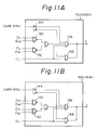
- Figs. 11A and 11B are diagrams each showing a specific construction of a region discriminator included in the embodiment of in Fig. 8; and
- Fig. 12 shows an example of signal regions as decided by the discriminators in relation to a 64 QAM modulated wave.
- Some embodiments of the present invention which are directed to achieving the object as previously stated will be described first.
- To better understand the present invention, a brief reference will be made to a prior art AGC circuit, shown in Fig. 1. The prior art AGC circuit, generally 10, comprises a baseband variable attenuator (ATT) 12, a 4-bits analog-to-digital (AD)
converter 14, an exclusive OR (Ex-OR)gate 16, and a low pass filter (LPF) 18. An 8-bits baseband signal, which is an input signal, is applied to theAD converter 14 via theATT 12. In response, theAD converter 14 regenerates main data signals D1 to D3, and an error signal D4. The signals D1 and D4 are routed to theEx-OR gate 16 which then produces a signal C1. The signal C1 is fed as a control signal to theATT 12 via theLPF 18 so as to control the input level of theAD converter 14 to an optimum one. - Referring to Fig. 2, a chart representative of the operation of the
AGC circuit 10 is shown. In Fig. 2, the 8-levels baseband signal is designated by d1 to d8 and the data outputted by the Ex-ORgate 16 by C1. When the input data d1 to d8 are remote from the center, or zero volt, i. e. , when the demodulation level is increased, all the outputs C1 become logical ZEROs; when the demodulation level is decreased, the outputs C1 become ONEs. This teachs that the output C1 serve as an error signal associated with theAGC circuit 10. - A false pull-in phenomenon will be described next. Assume that a modulated signal d'1 to d'8 having a value which is 7/9 of a regular level is initially applied to the
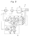
AD converter 14. In this condition, ZEROs and ONEs appear with the same probability on the output C1 of theEx-OR gate 16, so the error signals nominally appear stable and thecircuit 10 does not behave to restore the demodulated signal to the regular level. In this manner, once entered into d'1 to d'8 as shown in Fig. 2, the demodulated signal cannot get out thereof, resulting in a false pull-in. - Referring to Fig. 3, an AGC circuit in accordance with one embodiment of the present invention is shown. The AGC circuit, generally 20, includes an
ATT 12, anAD converter 14 and aLPF 18 which share the same functions as those of the priorart AGC circuit 10. Asubtractor 22 is interconnected between theATT 12 and theAD converter 14, and alogic circuit 24 between theAD converter 14 and theATT 12. Further, asecond logic circuit 26 is interconnected between thelogic circuit 24 and thesubtractor 22. Thelogic circuit 24 comprises an OR/NOR gates gates selector 40, a flip-flop 42, and aLPF 18. Theother logic circuit 26, on the other hand, comprises aselector 44, a flip-flop 46, and aLPF 48. A demodulated signal is routed through theATT 12 andsubtractor 22 to theAD converter 14 to be thereby converted to data sequences D1 to D4. When the demodulated signal inputted is at regular levels as represented by d1 to d8 in Fig. 2, theAD converter 14 produces signals D1 to D4 as shown on the right-hand side in Fig. 2. Thefirst logic circuit 24 is adapted to produce an error signal which is the characteristic feature of this particular embodiment. As shown in Fig. 2, threedifferent signal regions 1 to 3 are defined. When the demodulated signal has entered thesignal regions logic circuit 24 controls theATT 12 to reduce the demodulated signal. Conversely, when the demodulated signal has entered theregion 2, thelogic circuit 24 delivers to the ATT 12 a control signal for magnifying the demodulated signal. This allows the demodulated signal to be stabilized in the regular state as shown in Fig. 2, in which d1 contacts theregion 1, d4 and d5 contacts theregion 2, and d8 contacts theregion 3. When the demodulated signal d'1 to d'8 has initially been applied to theAD converter 14, d'4 and d'5 enter theregion 2 but not theregions ATT 12 until d'1 and d'8 respectively enter theregions circuit 20 with such a construction is free from false pull-in. - Referring to Fig. 3, a signal b1 becomes a ONE in response to the
regions flop 42 and, thereby, make an output of the flip-flop 42 a ZERO. A signal b2 becomes a ONE in response to theregion 2 to set the flip-flop 42 to turn an output thereof into a ONE. Here, let a ONE be a positive voltage and a ZERO a negative voltage. Then, if theATT 12 has such a characteristic that the amount of attenuation is decreased in response to a positive voltage and increased in response to a negative voltage, the above-stated operation is accomplished by applying an output of the flip-flop 42 to theATT 12 via theLPF 18 which is adapted for jitter suppression. Thesecond logic circuit 26 and thesubtractor 22 in combination constitute a circuit for compensating for DC drifts as are contained in a demodulated signal on the input of theAD converter 14. For details of operation of such a circuit, a reference may be made to JP-A-59174058. It is to be noted that this DC voltage control circuit is not essential although preferable for more accurate operation of theAGC circuit 20. - In Fig. 2, the
regions 1 to 3 are shown in relation to an 8-levels demodulated signal; theregion 1 contacting d1 from outside, theregion 2 contacting d4 and d5 from inside, and theregion 3 contacting d8 from outside. However, as the number of levels is increased such as to sixteen levels, simply defining theregions 1 to 3 at the outermost points and innermost point excessively limits the number of signal points which are available for control. The increase in the number of levels may be coped with by defining several zones inclusive of the outermost and innermost points so as to increase the number of signals available for control while preserving the advantage of the present invention. - Referring to Fig. 4, specific constructions of the
selectors selector 40 is made up of ANDgates 401 to 404 and ORgates selector 44, on the other hand, is made up of ANDgates - Referring to Fig. 5, another embodiment of the present invention which is applied to a 64 QAM demodulator is shown. The AGC circuit shown in Fig. 5 and generally designated by the
reference numeral 50 comprises an intermediate frequency (IF)band variable attenuator 52, aquadrature detector 54, subtractors 56 and 58, 4-bits AD converters adder 64, alogic circuit 66, a voltage controlled oscillator (VCO) 68, twofirst logic circuits 24 and twosecond logic circuits 26. In this particular embodiment, a 64 QAM modulated wave is routed via thevariable attenuator 52 to thequadrature detector 54 to be detected and thereby converted to 8-levels demodulated signals as represented by P and Q. Because the signals P and Q are exactly the same as the input signals as shown in Fig. 3, the operations of thesubtractors second logic circuits 26 are almost the same as those previously described. The difference is that in Fig. 5 outputs of the twofirst logic circuits 24 are added by theadder 64, so thevariable attenuator 52 may be controlled by the resultant sum. - The
variable attenuator 52 may be replaced with two such attenuators which are assigned one to the baseband of P and the other to that of Q. Further, one baseband variable attenuator and one IF band variable attenuator may be assigned to one of P and Q, as disclosed in JP-A-59169256. A reference carrier wave which is necessary for quadrature detection is regenerated by thelogic circuit 66 andVCO 68. For details of such regeneration, a reference may be made to JP-A-57131151. - Referring to Fig. 6, another embodiment of the present invention which is also applied to a 64 QAM demodulator is shown. The AGC circuit, generally 70, is substantially the same in construction and operation as the
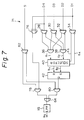
AGC circuit 50 of Fig. 5 except for a carrierasynchronism detection circuit 72 andfirst logic circuits 74. TheAGC circuit 70 is constructed to switch control signals from one to the other depending upon the steady/transitional state of the 64 QAM demodulator. Specifically, whether the demodulator is in a steady state or in a transitional state is determined by checking whether the carrier asynchronism detection circuit, or detector, 72 is in a synchronous state or in an asynchronous state. Then, if it is in a transitional state, control signals in accordance with this embodiment are used in order to avoid false pull-in and, if it is in a steady state, prior art control signals. The advantage attainable with such a construction is that because in a steady state which is free from the possibility of false pull-in all the signals are used as control signals, use can be made of prior art control signals which have an excellent jitter characteristic. As previously stated, the number of signal points usable as control signals of the present invention decreases with the increase in the number of levels, preventing the jitter characteristic from being deteriorated. Thecarrier asynchronism detector 72 may be implemented with a detector of the type utilizing the fact that the loop impedance of a carrier synchronizing circuit is high under an asynchronous state and low under a synchronous state. - Referring to Fig. 7, a specific construction of the
logic circuits 74 as shown in Fig. 6 is shown. In Fig. 7, the same or similar structural elements as those of Fig. 3 are designated by like reference numerals. Thelogic circuit 74 comprises anEx-OR gate 76, ANDgates gate 82 having an inverting and a non-inverting output andOR gate 84. The output of theEx-OR gate 76 is a prior art control signal while the output of the flip-flop 42 is a control signal in accordance with the present invention. The two outputs are switched from one to the other by a switching signal S. - In the embodiment of Fig. 6, while the demodulator is in a transitional state, an AGC signal b5 is outputted when the output states of P and Q are in the
signal regions 1 to 3 of Fig. 2. Alternatively, an arrangement may be made such that the control signal b5 is outputted only when the output states of P and Q enter theregions 1 to 3 at the same time. This alternative scheme is advantageous in that even in a transitional state of the demodulator the signals (d1, d4, d5 and d8) can be identified and regenerated in the same conditions as during a steady state, enhancing the pull-in characteristic during a transitional state. - While the embodiments of Figs. 3 and 5 have been shown and described in relation to an 8-levels baseband signal, such is only illustrative and they are naturally applicable to baseband signals having two or more levels.
- It will be seen from the foregoing that the embodiments of the present invention elaborated to achieve the object as previously stated eliminate false pull-in to ensure stable pull-in operations and are applicable to baseband signals having two or more levels as well as to a 16 QAM system in microwave digital communication, enhancing reliability of operation of such systems.
- Some embodiments in which the AGC circuit according to the present invention can be used will be described in detail. The following demodulation system has been made the subject of a divisional application.
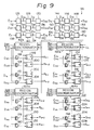
- Referring to Fig. 8, an exemplary digital demodulation system to which the present invention is applicable is shown. The system of Fig. 8, generally 90, comprises an IF band
transversal equalizer 92 and ademodulator 94. Theequalizer 92 is made up of a weightingcontrol signal generator 96, atransversal filter 98,adders subtractors demodulator 94, on the other hand, is made up of aquadrature detector 118, 3-bits AD converters 120 and 122, and acarrier regenerator 124. An exemplary construction of the weightingcontrol signal generator 96 is shown in Fig. 9. As shown in Fig. 9, thegenerator 96 comprises 1-bit delay lines region discriminators Ex-OR gates flops - An input signal, or 16 QAM modulated wave, is applied to the
transversal filter 98 which is made up of a delay circuit and a weighting circuit. Thetransversal filter 98 functions to compensate for intersymbol interference which is contained in the input signal. The weighting circuit is controlled by signals R±1, R±2, I±1 and I±2 which are the results of addition or subtraction of the outputs of the weightingcontrol signal generator 96. The basic operation of the transversal equalizer is disclosed in, for example, a paper entitled "Demodulator with 4/5GHz 16QAM 200 Mb/s Transversal Equalizer" which was presented at the 1984 National Meeting of Institute of Electronic Engineers, Communications Section, No. 628. - The output of the
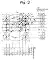
transversal equalizer 92 is applied to thedemodulator 94 and detected by thequadrature detector 118, thereby being turned into demodulated baseband signals P and Q. The baseband signals P and Q are converted to digital signals by the 3-bits AD converters 120 and 122, respectively. Then, the AD converter 120 regenerates main signals D1p and D2p and an error signal Ep while theAD converter 122 regenerates main signals D1q and D2q and an error signal Eq. The regenerated signals and the input signals are related as shown in Fig. 10. In Fig. 10, a₁ to a₁₆ are representative of the input signals, D1q, D2q and Eq the outputs of theAD converter 122, and D1p, D2p and Ep the outputs of the AD converter 120. All the regenerated signals are applied to the weightingcontrol signal generator 96 to generate control signals. A part of the regenerated signals is applied to thecarrier regenerator 124 to recover a reference carrier wave which is necessary for synchronous detection. The construction and operation of thecircuit 124 is described in detail in Japanese Patent Application No. 56-15775 and, therefore, description thereof will be omitted herein. A reset signal R outputted by thecarrier regenerator 124 is a signal adapted to show whether theregenerator 124 is in a synchronous state or in an asynchronous state and is applied to the weightingcontrol signal generator 96. - The weighting
control signal generator 96 is one of characteristic features of the present invention and will be described in detail hereinafter. - The construction shown in Fig. 9 includes
region discriminators flops demodulator 94 is in an asynchronous state. Then, the signals a₁ to a₁₆ go round the circles m₁ to m₃. Assuming that the respective signals are subjected to intersymbol interference of real number portions (identical in phase and polarity), the signals a₁, a₅ and a₁₃, for example, are shifted to a'₁, a'₅ and a'₁₃, respectively. Meanwhile, if thedemodulator 94 is in a synchronous state, the signals a₁, a₅ and a₁₃ respectively remain in the positions a'₁, a'₅ and a₁₃ and, in this condition, correct error signals are produced to promote convergence. - However, while the
demodulator 94 is in an asynchronous state, the respective signal points go round the circles m₁ to m₃ with the result that the signal a'₅ enter the position a''₅. In this condition, a''₅ lies in the signal region of a₁, so the signal a₁ appears as if it were a signal a''₁ which has been subjected to intersymbol interference of the same phase and the opposite polarity. The result is the generation of incorrect error signals. Such an operation applies to all the signals a₅ to a₁₂ having middle levels. In this situation, the incorrect error signals become greater than the correct ones to cause the weightingcontrol signal generator 96 associated with real number portions to malfunction, thereby preventing the prior art digital demodulation system from being restored to normal. The same mechanism of malfunction applies to a weighting control signal generator which is associated with imaginary number portions. - The
region discriminators storages region discriminators region discriminators Ex-OR gates flops region discriminators region discriminators discriminators region discriminators - The
region discriminators demodulator 94 is in a normal state, i. e., when thecarrier regenerator 124 is in a synchronous state. Specifically, when the reset signal R has disappeared, clock pulses are continuously delivered as signals X and Y so as to make the flip-flops 198 to 228 through with the result that the same control signals as in a prior art circuit are produced. - The advantage of the above-described construction is as follows. The region discriminators in this particular embodiment are capable of recovering the demodulation system even if the
demodulator 94 is in an asynchronous state with input signals subjected to significant intersymbol interference. However, the number of signal points used as control signals is small; for example, in the case of 16 QAM system as shown in Fig. 10, only 1/4 of the signal points is used. The proportion of the signal points used sequentially decreases as the number of levels of input signals is increased. Because a decrease in the proportion of signal points used is reflected by an increase in jitter which is contained in control signals, it is preferable that while the demodulator is normal, use is made of the prior art construction which prepares control signals using all the signals. Thus, in accordance with this embodiment the region discriminators operate nominally with the same construction as the prior art ones so long as the demodulator is in a normal state, as previously stated. - Referring to Figs. 11A and 11B, specific constructions of the
region discriminators 162a (162b) and 164a (164b) are shown. Theregion discriminator 162a (162b) comprisesEx-OR gates gate 134, and ANDgates region discriminator 164a (164b), on the other hand, comprisesEx-OR gates gate 144, and ANDgates - Although this particular embodiment is applicable to high multi-level modulation systems having sixteen or more levels, too, an increase in the number of levels makes the number of signal points usable as control signals extremely small.
- Referring to Fig. 12, there is shown one example of discrimination regions which are associated with a real number portion control circuit for 64 QAM modulated waves. As shown, there are defined a signal region A which contacts the maximum level signals of demodulated signals P and Q from outside and a region A' which contacts the minimum level signals from inside. In this case, the regions are defined for each of P and Q. In this manner, the regions A and A' are adequately set up in matching relation to the number of levels and the arrangement of signal points.
- While in Fig. 8 the transversal equalizer has been shown in relation to the IF band, use may be made of a baseband transversal equalizer, in which case the outputs of the weighting control signal generator will be directly applied to P and Q baseband transversal filters. Where this embodiment is applied to a high multi-level modulation wave having sixteen or more levels, what is required is simply increasing the number of bits of the
AD converters 120 and 122 of Fig. 8 and modifying the regions to be discriminated by thediscriminators - As described above, in accordance with the embodiment described above, the digital demodulation system is capable of being restored to normal even if a demodulator is in an asynchronous state and input signals involve significant intersymbol interference. This allows a transversal equalizer included in the system to fully exhibit an equalizing function thereof.
Claims (5)
- An automatic gain control circuit for controlling an input level of a multi-level discriminator (14) to an optimum level to discriminate a multi-level baseband signal in terms of multiple levels, comprising:
a variable attenuator (12) responsive to one of an intermediate frequency band or a baseband and interconnected to the multi-level discriminator (14) for varying an input level of the discriminator (14);
characterized by
identifying means (28-40) for identifying, in response to an output of the multi-level discriminator (14), at least a first to a third region being related to levels of a demodulated signal, such that the first and third region are defined at the outermost points and the second region is defined at the innermost point; and
logic means (42, 18) being connected to the identifying means (28-40) to generate a control signal for controlling said variable attenuator (12) such that the gain of the variable attenuator (12) is reduced when the output of the identifying means is representative of the first region or the third region, while the gain of the variable attenuator (12) is increased when the output of the identifying means is representative of the second region. - An automatic gain control circuit according to claim 1 wherein said logic means comprises a set-reset flip-flop (42) connected to said identifying means (28-40), and a low pass filter (18) for generating said control signal by smoothing the output of said flip-flop (42).
- An automatic gain control circuit according to claim 1 or 2, further comprising a second logic circuit (26) being connected to said identifying means (28-40) and providing a signal to a subtractor (22) being serially connected to the multi-level discriminator (14).
- An automatic gain control circuit according to claim 3 wherein said second logic circuit (26) comprises a selector (44), a set-reset flip-flop (46) and a low pass filter (48).
- Use of an automatic gain control circuit according to any of claims 1 to 4 in a demodulator (50, 70, 94) in a digital demodulation system.
Priority Applications (1)
| Application Number | Priority Date | Filing Date | Title |
|---|---|---|---|
| EP92103182A EP0486474B1 (en) | 1985-06-29 | 1986-06-27 | Method for adapting a transversal equalizer, without carrier synchronism |
Applications Claiming Priority (4)
| Application Number | Priority Date | Filing Date | Title |
|---|---|---|---|
| JP141529/85 | 1985-06-29 | ||
| JP60141529A JPH0797746B2 (en) | 1985-06-29 | 1985-06-29 | Automatic gain control circuit |
| JP60149931A JPH0697755B2 (en) | 1985-07-10 | 1985-07-10 | Digital demodulation system |
| JP149931/85 | 1985-07-10 |
Related Child Applications (1)
| Application Number | Title | Priority Date | Filing Date |
|---|---|---|---|
| EP92103182.9 Division-Into | 1986-06-27 |
Publications (3)
| Publication Number | Publication Date |
|---|---|
| EP0213309A2 EP0213309A2 (en) | 1987-03-11 |
| EP0213309A3 EP0213309A3 (en) | 1989-04-05 |
| EP0213309B1 true EP0213309B1 (en) | 1994-01-05 |
Family
ID=26473745
Family Applications (2)
| Application Number | Title | Priority Date | Filing Date |
|---|---|---|---|
| EP86108803A Expired - Lifetime EP0213309B1 (en) | 1985-06-29 | 1986-06-27 | Automatic gain control circuit |
| EP92103182A Expired - Lifetime EP0486474B1 (en) | 1985-06-29 | 1986-06-27 | Method for adapting a transversal equalizer, without carrier synchronism |
Family Applications After (1)
| Application Number | Title | Priority Date | Filing Date |
|---|---|---|---|
| EP92103182A Expired - Lifetime EP0486474B1 (en) | 1985-06-29 | 1986-06-27 | Method for adapting a transversal equalizer, without carrier synchronism |
Country Status (5)
| Country | Link |
|---|---|
| US (1) | US4703282A (en) |
| EP (2) | EP0213309B1 (en) |
| AU (1) | AU579554B2 (en) |
| CA (2) | CA1282127C (en) |
| DE (2) | DE3650568T2 (en) |
Families Citing this family (30)
| Publication number | Priority date | Publication date | Assignee | Title |
|---|---|---|---|---|
| JPS62298255A (en) * | 1986-06-18 | 1987-12-25 | Fujitsu Ltd | Identifying device |
| CA1287383C (en) * | 1986-07-09 | 1991-08-06 | Shoichi Mizoguchi | 8-phase phase-shift keying demodulator |
| JPS6387828A (en) * | 1986-09-30 | 1988-04-19 | Nec Corp | Digital demodulation system |
| US4759036A (en) * | 1987-03-02 | 1988-07-19 | American Telephone And Telegraph Company | Decision-directed control circuit |
| CA1278610C (en) * | 1987-09-21 | 1991-01-02 | Eisaku Sasaki | Stepped square-qam demodulator utilizing all signal points to generate control signals |
| US4995106A (en) * | 1989-08-24 | 1991-02-19 | Ampex Corporation | Fast decision feedback decoder for digital data |
| FI85548C (en) * | 1990-06-14 | 1992-04-27 | Nokia Oy Ab | Receiving procedure and receivers for discrete signals |
| US5097486A (en) * | 1990-07-31 | 1992-03-17 | Ampex Corporation | Pipelined decision feedback decoder |
| JP2794964B2 (en) * | 1991-02-27 | 1998-09-10 | 日本電気株式会社 | Control signal generation circuit |
| AU673390B2 (en) * | 1993-01-20 | 1996-11-07 | Nec Corporation | An AGC circuit for burst signal |
| FR2688367A1 (en) * | 1993-03-01 | 1993-09-10 | Alcatel Nv | Automatic gain control in a radio frequency receiver including a time-based equaliser circuit |
| JP2911773B2 (en) * | 1994-03-18 | 1999-06-23 | 富士通株式会社 | Digital multiplex radio receiver |
| GB2323505B (en) * | 1994-03-18 | 1998-11-04 | Fujitsu Ltd | Radio receiver for use in the reception of digital multiplexing signals |
| US5828692A (en) * | 1995-12-06 | 1998-10-27 | Rockwell International Corporation | Baseband demodulator for polar or rectangular modulated signal in a cordless spread spectrum telephone |
| KR100241890B1 (en) | 1997-01-10 | 2000-03-02 | 윤종용 | Circuit for removing interference in digital communication system |
| US6546063B1 (en) | 1998-02-10 | 2003-04-08 | Agere Systems Inc. | Asynchronous clock for adaptive equalization |
| US6038266A (en) * | 1998-09-30 | 2000-03-14 | Lucent Technologies, Inc. | Mixed mode adaptive analog receive architecture for data communications |
| US6680985B1 (en) * | 2000-08-15 | 2004-01-20 | Hughes Electronics Corporation | Adaptive quadrature amplitude modulation decoding system |
| JP3594297B2 (en) * | 2000-11-08 | 2004-11-24 | 株式会社日立国際電気 | Data reproduction method and data regenerator |
| US7764757B2 (en) | 2006-05-30 | 2010-07-27 | Fujitsu Limited | System and method for the adjustment of offset compensation applied to a signal |
| US7839958B2 (en) | 2006-05-30 | 2010-11-23 | Fujitsu Limited | System and method for the adjustment of compensation applied to a signal |
| US7839955B2 (en) | 2006-05-30 | 2010-11-23 | Fujitsu Limited | System and method for the non-linear adjustment of compensation applied to a signal |
| US7817757B2 (en) | 2006-05-30 | 2010-10-19 | Fujitsu Limited | System and method for independently adjusting multiple offset compensations applied to a signal |
| US7848470B2 (en) * | 2006-05-30 | 2010-12-07 | Fujitsu Limited | System and method for asymmetrically adjusting compensation applied to a signal |
| US7801208B2 (en) * | 2006-05-30 | 2010-09-21 | Fujitsu Limited | System and method for adjusting compensation applied to a signal using filter patterns |
| US7787534B2 (en) | 2006-05-30 | 2010-08-31 | Fujitsu Limited | System and method for adjusting offset compensation applied to a signal |
| US7804921B2 (en) | 2006-05-30 | 2010-09-28 | Fujitsu Limited | System and method for decoupling multiple control loops |
| US7760798B2 (en) | 2006-05-30 | 2010-07-20 | Fujitsu Limited | System and method for adjusting compensation applied to a signal |
| US7817712B2 (en) | 2006-05-30 | 2010-10-19 | Fujitsu Limited | System and method for independently adjusting multiple compensations applied to a signal |
| US7804894B2 (en) | 2006-05-30 | 2010-09-28 | Fujitsu Limited | System and method for the adjustment of compensation applied to a signal using filter patterns |
Family Cites Families (11)
| Publication number | Priority date | Publication date | Assignee | Title |
|---|---|---|---|---|
| US4283682A (en) * | 1979-04-06 | 1981-08-11 | Ricoh Company, Ltd. | Erasure zone decision feedback phase lock loop for carrier recovery in data modems |
| JPS5615775A (en) | 1979-07-18 | 1981-02-16 | Hideaki Sasaki | Ball safe device for pinball machine |
| JPS57131151A (en) | 1981-02-06 | 1982-08-13 | Nec Corp | Carrier wave reproducing circuit |
| JPS5962228A (en) | 1982-10-01 | 1984-04-09 | Nec Corp | Automatic equalizer |
| JPH063947B2 (en) | 1983-03-16 | 1994-01-12 | 日本電気株式会社 | Automatic gain control circuit |
| US4544894A (en) * | 1983-03-23 | 1985-10-01 | Nec Corporation | DC Voltage control circuits |
| JPS59174058A (en) | 1983-03-23 | 1984-10-02 | Nec Corp | Dc voltage control circuit |
| US4602374A (en) * | 1984-02-27 | 1986-07-22 | Nippon Telegraph & Telephone Public Corporation | Multi-level decision circuit |
| JPS6156555A (en) * | 1984-08-27 | 1986-03-22 | Nec Corp | Demodulator |
| JPS61112414A (en) * | 1984-11-06 | 1986-05-30 | Nec Corp | Automatic level control circuit |
| JPS61137446A (en) * | 1984-12-10 | 1986-06-25 | Nec Corp | Demodulating device |
-
1986
- 1986-06-26 US US06/878,746 patent/US4703282A/en not_active Expired - Lifetime
- 1986-06-26 CA CA000512494A patent/CA1282127C/en not_active Expired - Lifetime
- 1986-06-27 DE DE3650568T patent/DE3650568T2/en not_active Expired - Lifetime
- 1986-06-27 AU AU59337/86A patent/AU579554B2/en not_active Expired
- 1986-06-27 EP EP86108803A patent/EP0213309B1/en not_active Expired - Lifetime
- 1986-06-27 EP EP92103182A patent/EP0486474B1/en not_active Expired - Lifetime
- 1986-06-27 DE DE86108803T patent/DE3689499T2/en not_active Expired - Lifetime
-
1990
- 1990-10-09 CA CA000615890A patent/CA1292525C/en not_active Expired - Lifetime
Also Published As
| Publication number | Publication date |
|---|---|
| CA1282127C (en) | 1991-03-26 |
| DE3650568T2 (en) | 1997-04-30 |
| CA1292525C (en) | 1991-11-26 |
| EP0213309A2 (en) | 1987-03-11 |
| EP0486474A3 (en) | 1992-08-12 |
| AU5933786A (en) | 1987-01-08 |
| EP0486474A2 (en) | 1992-05-20 |
| DE3689499T2 (en) | 1994-04-28 |
| DE3689499D1 (en) | 1994-02-17 |
| DE3650568D1 (en) | 1996-10-17 |
| AU579554B2 (en) | 1988-11-24 |
| EP0213309A3 (en) | 1989-04-05 |
| US4703282A (en) | 1987-10-27 |
| EP0486474B1 (en) | 1996-09-11 |
Similar Documents
| Publication | Publication Date | Title |
|---|---|---|
| EP0213309B1 (en) | Automatic gain control circuit | |
| US4484337A (en) | Carrier wave regenerating circuit | |
| EP0120416B1 (en) | Demodulator with automatic gain control circuit | |
| US4458356A (en) | Carrier recovery circuit | |
| US4553102A (en) | Multilevel amplitude modulation demodulator with DC drift compensation | |
| EP0118119B1 (en) | Timing synchronizing circuit | |
| JPH02131031A (en) | Demodulator | |
| EP0120474B1 (en) | Dc voltage control circuits | |
| JPS6387828A (en) | Digital demodulation system | |
| US4466109A (en) | Carrier recovery arrangement for sixteen-state amplitude and phase modulation and receiving system for digital data, comprising such an arrangement | |
| EP0212582B1 (en) | Demodulation system capable of establishing synchronization in a transient state | |
| US4803438A (en) | 8-phase phase-shift keying demodulator | |
| EP0184805B1 (en) | Demodulator | |
| US4498050A (en) | Demodulation device for composite PSK-PSK modulated waves | |
| JP2534650B2 (en) | Demodulator | |
| JP2526540B2 (en) | Carrier wave synchronization circuit | |
| JPH0515336B2 (en) | ||
| JP2564840B2 (en) | Digital demodulator | |
| JP2560339B2 (en) | Digital demodulator | |
| JP2871172B2 (en) | Demodulator | |
| JPS6239923A (en) | Demodulation system | |
| JP2540958B2 (en) | Digital modulation / demodulation system | |
| JPH0712178B2 (en) | Digital modulation / demodulation system | |
| JPH0797746B2 (en) | Automatic gain control circuit | |
| JPH0697755B2 (en) | Digital demodulation system |
Legal Events
| Date | Code | Title | Description |
|---|---|---|---|
| PUAI | Public reference made under article 153(3) epc to a published international application that has entered the european phase |
Free format text: ORIGINAL CODE: 0009012 |
|
| 17P | Request for examination filed |
Effective date: 19860627 |
|
| AK | Designated contracting states |
Kind code of ref document: A2 Designated state(s): DE FR GB IT NL SE |
|
| PUAL | Search report despatched |
Free format text: ORIGINAL CODE: 0009013 |
|
| AK | Designated contracting states |
Kind code of ref document: A3 Designated state(s): DE FR GB IT NL SE |
|
| 17Q | First examination report despatched |
Effective date: 19910424 |
|
| RTI1 | Title (correction) | ||
| GRAA | (expected) grant |
Free format text: ORIGINAL CODE: 0009210 |
|
| AK | Designated contracting states |
Kind code of ref document: B1 Designated state(s): DE FR GB IT NL SE |
|
| PG25 | Lapsed in a contracting state [announced via postgrant information from national office to epo] |
Ref country code: IT Free format text: LAPSE BECAUSE OF FAILURE TO SUBMIT A TRANSLATION OF THE DESCRIPTION OR TO PAY THE FEE WITHIN THE PRE;WARNING: LAPSES OF ITALIAN PATENTS WITH EFFECTIVE DATE BEFORE 2007 MAY HAVE OCCURRED AT ANY TIME BEFORE 2007. THE CORRECT EFFECTIVE DATE MAY BE DIFFERENT FROM THE ONE RECORDED.SCRIBED TIME-LIMIT Effective date: 19940105 Ref country code: NL Effective date: 19940105 Ref country code: SE Effective date: 19940105 Ref country code: FR Effective date: 19940105 |
|
| XX | Miscellaneous (additional remarks) |
Free format text: TEILANMELDUNG 92103182.9 EINGEREICHT AM 27/06/86. |
|
| REF | Corresponds to: |
Ref document number: 3689499 Country of ref document: DE Date of ref document: 19940217 |
|
| EN | Fr: translation not filed | ||
| NLV1 | Nl: lapsed or annulled due to failure to fulfill the requirements of art. 29p and 29m of the patents act | ||
| PLBE | No opposition filed within time limit |
Free format text: ORIGINAL CODE: 0009261 |
|
| STAA | Information on the status of an ep patent application or granted ep patent |
Free format text: STATUS: NO OPPOSITION FILED WITHIN TIME LIMIT |
|
| 26N | No opposition filed | ||
| REG | Reference to a national code |
Ref country code: GB Ref legal event code: IF02 |
|
| PGFP | Annual fee paid to national office [announced via postgrant information from national office to epo] |
Ref country code: GB Payment date: 20050622 Year of fee payment: 20 |
|
| PGFP | Annual fee paid to national office [announced via postgrant information from national office to epo] |
Ref country code: DE Payment date: 20050623 Year of fee payment: 20 |
|
| REG | Reference to a national code |
Ref country code: GB Ref legal event code: PE20 |
|
| PG25 | Lapsed in a contracting state [announced via postgrant information from national office to epo] |
Ref country code: GB Free format text: LAPSE BECAUSE OF EXPIRATION OF PROTECTION Effective date: 20060626 |