EP0237151A1 - Infrared process and apparatus for infrared soldering components on circuit boards - Google Patents
Infrared process and apparatus for infrared soldering components on circuit boards Download PDFInfo
- Publication number
- EP0237151A1 EP0237151A1 EP87300480A EP87300480A EP0237151A1 EP 0237151 A1 EP0237151 A1 EP 0237151A1 EP 87300480 A EP87300480 A EP 87300480A EP 87300480 A EP87300480 A EP 87300480A EP 0237151 A1 EP0237151 A1 EP 0237151A1
- Authority
- EP
- European Patent Office
- Prior art keywords
- components
- heat
- zone
- soldering
- heat sink
- Prior art date
- Legal status (The legal status is an assumption and is not a legal conclusion. Google has not performed a legal analysis and makes no representation as to the accuracy of the status listed.)
- Granted
Links
Images

Classifications
-
- H—ELECTRICITY
- H05—ELECTRIC TECHNIQUES NOT OTHERWISE PROVIDED FOR
- H05K—PRINTED CIRCUITS; CASINGS OR CONSTRUCTIONAL DETAILS OF ELECTRIC APPARATUS; MANUFACTURE OF ASSEMBLAGES OF ELECTRICAL COMPONENTS
- H05K13/00—Apparatus or processes specially adapted for manufacturing or adjusting assemblages of electric components
- H05K13/04—Mounting of components, e.g. of leadless components
- H05K13/046—Surface mounting
- H05K13/0465—Surface mounting by soldering
-
- B—PERFORMING OPERATIONS; TRANSPORTING
- B23—MACHINE TOOLS; METAL-WORKING NOT OTHERWISE PROVIDED FOR
- B23K—SOLDERING OR UNSOLDERING; WELDING; CLADDING OR PLATING BY SOLDERING OR WELDING; CUTTING BY APPLYING HEAT LOCALLY, e.g. FLAME CUTTING; WORKING BY LASER BEAM
- B23K1/00—Soldering, e.g. brazing, or unsoldering
- B23K1/005—Soldering by means of radiant energy
- B23K1/0053—Soldering by means of radiant energy soldering by means of I.R.
-
- H—ELECTRICITY
- H05—ELECTRIC TECHNIQUES NOT OTHERWISE PROVIDED FOR
- H05K—PRINTED CIRCUITS; CASINGS OR CONSTRUCTIONAL DETAILS OF ELECTRIC APPARATUS; MANUFACTURE OF ASSEMBLAGES OF ELECTRICAL COMPONENTS
- H05K3/00—Apparatus or processes for manufacturing printed circuits
- H05K3/30—Assembling printed circuits with electric components, e.g. with resistor
- H05K3/32—Assembling printed circuits with electric components, e.g. with resistor electrically connecting electric components or wires to printed circuits
- H05K3/34—Assembling printed circuits with electric components, e.g. with resistor electrically connecting electric components or wires to printed circuits by soldering
- H05K3/3494—Heating methods for reflowing of solder
-
- H—ELECTRICITY
- H05—ELECTRIC TECHNIQUES NOT OTHERWISE PROVIDED FOR
- H05K—PRINTED CIRCUITS; CASINGS OR CONSTRUCTIONAL DETAILS OF ELECTRIC APPARATUS; MANUFACTURE OF ASSEMBLAGES OF ELECTRICAL COMPONENTS
- H05K2203/00—Indexing scheme relating to apparatus or processes for manufacturing printed circuits covered by H05K3/00
- H05K2203/11—Treatments characterised by their effect, e.g. heating, cooling, roughening
- H05K2203/1121—Cooling, e.g. specific areas of a PCB being cooled during reflow soldering
-
- H—ELECTRICITY
- H05—ELECTRIC TECHNIQUES NOT OTHERWISE PROVIDED FOR
- H05K—PRINTED CIRCUITS; CASINGS OR CONSTRUCTIONAL DETAILS OF ELECTRIC APPARATUS; MANUFACTURE OF ASSEMBLAGES OF ELECTRICAL COMPONENTS
- H05K2203/00—Indexing scheme relating to apparatus or processes for manufacturing printed circuits covered by H05K3/00
- H05K2203/30—Details of processes not otherwise provided for in H05K2203/01 - H05K2203/17
- H05K2203/304—Protecting a component during manufacturing
-
- H—ELECTRICITY
- H05—ELECTRIC TECHNIQUES NOT OTHERWISE PROVIDED FOR
- H05K—PRINTED CIRCUITS; CASINGS OR CONSTRUCTIONAL DETAILS OF ELECTRIC APPARATUS; MANUFACTURE OF ASSEMBLAGES OF ELECTRICAL COMPONENTS
- H05K3/00—Apparatus or processes for manufacturing printed circuits
- H05K3/30—Assembling printed circuits with electric components, e.g. with resistor
- H05K3/32—Assembling printed circuits with electric components, e.g. with resistor electrically connecting electric components or wires to printed circuits
- H05K3/34—Assembling printed circuits with electric components, e.g. with resistor electrically connecting electric components or wires to printed circuits by soldering
- H05K3/341—Surface mounted components
- H05K3/3415—Surface mounted components on both sides of the substrate or combined with lead-in-hole components
Definitions
- This invention relates to the infrared soldering of components on circuit boards by infrared radiation, and in particular to the infrared soldering of surface mounted components. More specifically, the invention is concerned with the infrared soldering of components, and in particular surface mounted components, on one surface of a circuit board after other components have been mounted on the other surface of the circuit board.
- Circuit boards very frequently have components on both surfaces of the board.
- a circuit pattern will be formed on one surface, with contact pads at various positions. Holes are provided through the board, aligned with some of the pads.
- leaded components are mounted on the surface remote from the circuit pattern via leads passed.through the holes and soldered t pads. Such soldering is usually done by wave soldering, although other forms of soldering can be used.
- other components, and in particular surface mounting components are mounted on the surface of the board on which is formed the circuit pattern. The soldering of these other components is obtained by various methods, one of which is infrared irradiation.
- a basic problem relating to the soldering of the components in the further step is obtaining satisfactory fusion or melting of the solder paste while at the same time avoiding melting of other solder joints, such as the solder attaching leaded components, which will be hanging down from what would be the lower surface of the board when the surface mounting components are being soldered. Even using a solder of lower melting point, in the second step, for the surface mounted and any other components does not provide a fully satisfactory answer.
- a further problem is that during heating of a circuit board prior to soldering of the further components, the previously soldered components can be heated to a temperature which can cause malfunction of the components or lead to a reduced operating life.
- the present invention provides an infrared soldering system in which the ci-cuit boards are maintained below the temperature normally attained by positioning a heat sink in one or more of the various heating zones, for example, the preheat zone, heat stabilizing zone, and high temperature soldering zone.
- the heat sink removes heat which otherwise would build up in spaces normally shielded by the circuit boards due to the infrared radiation heating such zones when boards are not in position. It is possible to produce a very high temperature in the joints to be soldered while maintaining the other joints at lower temperatures. Also, previously mounted components are kept at a lower temperature.
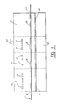
- FIG. 1 illustrates an infrared (IR) furnace 10 through which passes a conveyor 11.
- the furnace in the particular example, has four zones, a preheat zone 12, a heat stabilizing zone 13, a heat "spike” zone 14 and a cooling zone 15.
- Circuit boards 16 are carried through the furnace 10 on the conveyor 11.
- the conveyor 11 comprises two parallel spaced apart belts or similar members which support the circuit boards 16 at their side edges, with components on the undersurface of a board projecting down between the belts. Heating of the boards is by IR radiation from IR lamps 17.
- the main heating zone 14 an intense level of heating occurs, for a relatively short time, to fuse the solder paste which has been deposited on the board.
- the IR lamps 17 in the main heating zone 14 create a "spike" of heat at about midpoint along the zone 14.
- the effect in zone 14 is to rapidly raise the heat to a high temperature for a short period of time.
- the maximum temperature is of the order of 188°C (370°F).
- the heat output from the lamps 17 is high in the preheat zone.
- the heat output is relatively low.
- the temperature of some components and parts reduces while the temperature of the remainder rises, to a low maximum. This enables thermal shock to be avoided for critical components and other parts and also gives time for the solder flux to activate and for the vo.latiles to be given off.
- the low maximum temperature is controlled by the liability of damage to components. Even though the final heating, in zone 14, is rapid and concentrated, it is still_possible that melting of previously soldered joints can occur. Also, some components can reach undesirable temperatures.
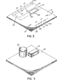
- FIGs 2 and 3 illustrate very diagrammatically both surfaces of a circuit board 16.
- a circuit pattern is formed, indicated generally at 20.
- a small number of surface mounted components are shown at 21.
- Also seen in Figure 2 are holes 22 through the circuit board. Leads from components on the other surface extend through the holes 22 and are soldered to the circuit pattern 20.
- Figure 3 shows two leaded components 23 mounted on the board 16, on the other surface to that shown in Figure 2.
- the leads of the components pass through holes in the circuit board as shown at 22 in Figure 2.
- several other leaded components are mounted on the surface shown in Figure 3.
- solder joints between the leaded components 23 and the circuit pattern 20 do not become molten during soldering of the surface mounted components 21. If the solder does melt, the components 23 are likely to fall off. At the same time, it is necessary to heat the proposed solder joints between the surface mounted components and the circuit pattern to as high a temperature as possible. If the temperature is too low then no fusion occurs at all. Solder paste is normally applied to contact areas on the circuit pattern and the temperature to which the paste is heated must be sufficient to activate the flux included in the paste, and also to melt the solder. At an intermediate temperature there is a sintering of the solder paste. Depending upon circumstances, this may or may not give an acceptable joint. Further, unless a certain minimal temperature is achieved, the activity of the flux is reduced and certain volatile components may not be driven off. This can result in unsatisfactory joints.
- the present invention proposes a substantial change in the hitherto standard process. Instead of bringing all of the circuit board and components up to a stable preheat, it is arranged that heat is abstracted below the conveyor level in the furnace to maintain a lower temperature for previously soldered components, for example, leaded components. Particularly, it is arranged that heat be abstracted below the conveyor or belt level in the solder melt zone, zone 14 in Figure 1.
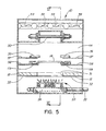
- Figures 4 and 5 illustrate the solder melt zone in a furnace, in accordance with the present invention.
- Figure 4 being a perspective with parts omitted to show detail
- Figure 5 being a cross-section.
- the preheat and stabilizing zones - zones 12 and 13 in Figure 1 - have been omitted so that details of the melt zone - zone 14 in Figure 1 - can be seen.
- the cooling zone 15 has also been omitted.
- the IR lamps are shown at 30. In the example, three lamps are provided extending transverse to the direction of travel in the circuit boards.
- the conveyor 11 is seen, composed of two parallel spaced link belts lla and llb.
- the refractory member 18 extends across the chamber, spaced down from the belts lla and llb, the refractory member having a window 31 therein.
- the refractory member 18 is supported by a metal sheet 32, seen in Figure 5.
- Beneath the refractory member is a heat sink 33 mounted on a cooling plate 34.
- the heat sink is composed of a finned body of heat absorbent material, for example aluminum, and the cooling plate 34 is, for example, of copper.
- the plate 34 is hollow and is cooled by a cooling fluid fed therethrough via tubes 35.
- the window 32 is necessary for two reasons. If the refractory member extended across the chamber unbroken, then it would be heated, when not shielded by a circuit board, by the IR radiation from bulbs 30. When a board passes through, this heat would be radiated back against the undersurface of the circuit board and against the components thereon, as described above in conjunction with Figure 1.
- the window permits the IR radiation to pass through and the energy is absorbed by the heat sink 33 and transferred to the cooling member 34 and then to the cooling fluid, if provided.
- the heat sink will abstract heat from the components mounted on the lower surface. This will maintain these components at a lower temperature than that which normally occurs. Also, the circuit board itself is at a lower temperature.
- fans 39 are provided for forcing air through the zone.
- heat shields 35 and 36 are provided, resting on shelves 37. The belts lla and llb are supported in guides 38.
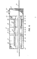
- FIG. 6 is a longitudinal cross-section through a furnace incorporating heat sinks 33, 34 in the preheat zone 12 and in the soldering zone 14. Also indicated in dotted outline are heat sinks 40, 41 in the heat stabilizing zone 13. Heat sinks 40, 41 may or may not be provided, depending upon requirements and accessability.
- a plurality of IR lamps 42 are provided in the preheat zone 12, while two lamps 43 are shown in the stabilizing zone 13. The number of lamps may vary, depending upon requirements.
- a ceramic member 44 is shown and also ceramic shields 45 are provided in the preheat zone.
- a window 46 is provided in ceramic member 44.
- ceramic shields 47 are provided, to protect the belts lla and llb.
- a ceramic member 48 is - provided below the link belts and a window 49 may or may not be provided in the ceramic member 48. Cooling air passes through the fans 39, issuing into the cooling zone 15. From here the air exhausts through an outlet 50.
- the final heating in zone 14 is normally arranged to give a high peak or "spike".
- the temperature at the solder joints for the surface mounting components can be as high as about 460°F (238°C). This is assisted by the situation that the shiny joint of previously soldered joints of the leaded components do not absorb heat from the IR as quickly as the duller solder paste. Thus the solder paste heats more quickly than the already soldered joints. Further, because the leaded components are cooled, heat is abstracted from the already soldered joints. As a result, although the solder paste is heated to a higher temperature, giving a very fluid melt to the solder with a resulting highly effective joint, the previously soldered joints are maintained below any temperature which will have an adverse effect on the joints.
- solder surface mounted components are usually very small, and relatively lightweight. It is possible to hold them in place with a solder paste/flux even when inverted.
- soldering positions there are two soldering positions spaced apart along a furnace.
- the lower surface of a circuit board is irradiated by IR lamps and the solder paste melted to solder the components onto the board.
- a heat sink and cooling member can be positioned in the upper part of the furnace to keep the upper surface cool, if desired.
- the upper surface is irradiated by IR lamps to melt the solder paste and solder the components in position.
- a heat sink and cooling member is mounted below the boards to keep the lower surface and components cool.
- the upper surface is first heated to solder the components on the upper surface, the lower surface and components thereon being kept cool by a heat sink and cooling member.
- the board is then turned over and the new upper surface heated to solder the components thereon.
- the previously soldered components, now on the lower surface, are kept cool by a heat sink and cooling member.
- preheat, heat stabilizing, soldering and cooling zones are usually provided for each soldering position.
- the furnaces illustrated, particularly in Figures 4 and 5, are generalized furnaces capable of processing circuit boards of various widths by varying the spacing of the belts 11. In an arrangement specifically designed for a single board width, or for a limited range of board widths, the furnace can be much narrower than that illustrated in Figures 4 and 5. Also, the vertical spacing of the various items, such as be ⁇ .s 11 and ceramic member 18 can be closer, enabling the heat sinks to be closer to the circuit board.
- Use of the invention enables the attachment of components to the board, on the side of the board remote from surface mounting components, prior to soldering the surface mounted components which previously were added afterwards. For example, a leaded relay can be soldered in position prior to soldering surface mounted components and not be damaged. The normal limit on such a relay is a maximum temperature of 120°C for one minute. The use of heat sinks enables this requirement to be met in spite of a higher soldering temperature for the surface mounting components than previously permitted.
- the invention has been particularly described with relation to the soldering of surface mounted components onto a surface of a circuit board on which other components have been soldered onto the other surface, the invention is not restricted to this.
- the invention can be used whenever it is desired to carry out a further soldering step on a circuit board after components have already been soldered on the board, and where it is necessaryy to avoid melting solder joints already made, or it is necessary to prevent previously soldered components reaching a temperature which can adversely affect the components, or both of these requirements.
- Fans can also be provided, in zones 12 and 13, to blow air from one zone, i.e. zone 12, to another zone, i.e. zone 14.
Abstract
Description
- This invention relates to the infrared soldering of components on circuit boards by infrared radiation, and in particular to the infrared soldering of surface mounted components. More specifically, the invention is concerned with the infrared soldering of components, and in particular surface mounted components, on one surface of a circuit board after other components have been mounted on the other surface of the circuit board.
- Circuit boards very frequently have components on both surfaces of the board. Thus, for example, a circuit pattern will be formed on one surface, with contact pads at various positions. Holes are provided through the board, aligned with some of the pads. In a first step, leaded components are mounted on the surface remote from the circuit pattern via leads passed.through the holes and soldered t pads. Such soldering is usually done by wave soldering, although other forms of soldering can be used. Following soldering of the leads, in a further step, other components, and in particular surface mounting components, are mounted on the surface of the board on which is formed the circuit pattern. The soldering of these other components is obtained by various methods, one of which is infrared irradiation.
- A basic problem relating to the soldering of the components in the further step is obtaining satisfactory fusion or melting of the solder paste while at the same time avoiding melting of other solder joints, such as the solder attaching leaded components, which will be hanging down from what would be the lower surface of the board when the surface mounting components are being soldered. Even using a solder of lower melting point, in the second step, for the surface mounted and any other components does not provide a fully satisfactory answer.
- A further problem is that during heating of a circuit board prior to soldering of the further components, the previously soldered components can be heated to a temperature which can cause malfunction of the components or lead to a reduced operating life.
- Various other problems exist in the process of mounting surface mounted components on boards to which other components have been mounted.
- The present invention provides an infrared soldering system in which the ci-cuit boards are maintained below the temperature normally attained by positioning a heat sink in one or more of the various heating zones, for example, the preheat zone, heat stabilizing zone, and high temperature soldering zone. The heat sink removes heat which otherwise would build up in spaces normally shielded by the circuit boards due to the infrared radiation heating such zones when boards are not in position. It is possible to produce a very high temperature in the joints to be soldered while maintaining the other joints at lower temperatures. Also, previously mounted components are kept at a lower temperature.
- The invention will be readily understood by the following description of certain embodiments, by way of example, in conjunction with the accompanying drawings, in which:-
- Figure 1 is a diagrammatic cross-section along a typical infrared heating furnace;
- Figures 2 and 3 are diagrammatic perspective views on the two surfaces of a circuit board;
- Figure 4 is a perspective view, partly sectioned, illustrating a heating zone of a furnace, in accordance with the present invention.
- Figure 5 is a cross-section generally on the line V-V of Figure 4; and
- Figure 6 is a longitudinal cross-section, similar to that of Figure 1, illustrating a furnace embodying the invention.
- Figure 1 illustrates an infrared (IR)
furnace 10 through which passes a conveyor 11. The furnace, in the particular example, has four zones, apreheat zone 12, aheat stabilizing zone 13, a heat "spike"zone 14 and acooling zone 15.Circuit boards 16 are carried through thefurnace 10 on the conveyor 11. Normally, the conveyor 11 comprises two parallel spaced apart belts or similar members which support thecircuit boards 16 at their side edges, with components on the undersurface of a board projecting down between the belts. Heating of the boards is by IR radiation fromIR lamps 17. - The
boards 16, on the conveyor 11, pass initially through thepreheat zone 12, then theheat stabilizing zone 13. In themain heating zone 14, an intense level of heating occurs, for a relatively short time, to fuse the solder paste which has been deposited on the board. TheIR lamps 17 in themain heating zone 14 create a "spike" of heat at about midpoint along thezone 14. The effect inzone 14 is to rapidly raise the heat to a high temperature for a short period of time. Typically, the maximum temperature is of the order of 188°C (370°F). - The heat output from the
lamps 17 is high in the preheat zone. In the stabilizing zone the heat output is relatively low. In the stabilizing zone the temperature of some components and parts reduces while the temperature of the remainder rises, to a low maximum. This enables thermal shock to be avoided for critical components and other parts and also gives time for the solder flux to activate and for the vo.latiles to be given off. The low maximum temperature is controlled by the liability of damage to components. Even though the final heating, inzone 14, is rapid and concentrated, it is still_possible that melting of previously soldered joints can occur. Also, some components can reach undesirable temperatures. - The situation is made worse by the fact that the
lamps 17 operate continuously, but the circuit boards are spaced apart along the conveyor, with gaps between them. Thus the energy from the IR lamps, particularly inzone 14, tends to heat up furnace members below the belts 11, for example, aceramic heat shield 18 positioned beneath the boards. This heat is redirected back to the undersurface of the boards as they pass through. Thus the boards and components are likely to be heated above an initial temperature. - Figures 2 and 3 illustrate very diagrammatically both surfaces of a
circuit board 16. On one surface a circuit pattern is formed, indicated generally at 20. In Figure 2, a small number of surface mounted components are shown at 21. Also seen in Figure 2 areholes 22 through the circuit board. Leads from components on the other surface extend through theholes 22 and are soldered to thecircuit pattern 20. - Figure 3 shows two leaded
components 23 mounted on theboard 16, on the other surface to that shown in Figure 2. The leads of the components pass through holes in the circuit board as shown at 22 in Figure 2. Generally, several other leaded components are mounted on the surface shown in Figure 3. - It will be appreciated that it is imperative that the solder joints between the
leaded components 23 and thecircuit pattern 20 do not become molten during soldering of the surface mountedcomponents 21. If the solder does melt, thecomponents 23 are likely to fall off. At the same time, it is necessary to heat the proposed solder joints between the surface mounted components and the circuit pattern to as high a temperature as possible. If the temperature is too low then no fusion occurs at all. Solder paste is normally applied to contact areas on the circuit pattern and the temperature to which the paste is heated must be sufficient to activate the flux included in the paste, and also to melt the solder. At an intermediate temperature there is a sintering of the solder paste. Depending upon circumstances, this may or may not give an acceptable joint. Further, unless a certain minimal temperature is achieved, the activity of the flux is reduced and certain volatile components may not be driven off. This can result in unsatisfactory joints. - Thus there is a situation in which compromises and "trade-offs" must be made. If a lower melting point solder is used for the surface mounting components, certain problems arise. Firstly, in operation, some of the surface mounted components can experience temperatures which can cause a chemical interaction between the solder and components, partly because of additives used to lower the melting point. Another problem is that the solder may soften or partially melt, allowing movement of a component. Also, even though the solder may melt during the IR heating, a lower preheat temperature may not result in good activity of the flux in the solder. Flux activity can be doubled by a 10°C rise in temperature. Also, it is necessary to drive off the volatiles from the solder paste before fusion, to avoid splatter and the like. The volatiles may not be properly driven off with a low temperature. Finally, in spite of the various difficulties it was found that the temperature differential was still insufficient to guarantee leaded components would not become unsoldered, or alternatively, poor quality solder joints for surface mounted components occurred.
- The present invention proposes a substantial change in the hitherto standard process. Instead of bringing all of the circuit board and components up to a stable preheat, it is arranged that heat is abstracted below the conveyor level in the furnace to maintain a lower temperature for previously soldered components, for example, leaded components. Particularly, it is arranged that heat be abstracted below the conveyor or belt level in the solder melt zone,
zone 14 in Figure 1. - Figures 4 and 5 illustrate the solder melt zone in a furnace, in accordance with the present invention. Figure 4 being a perspective with parts omitted to show detail, and Figure 5 being a cross-section. The preheat and stabilizing zones -
zones zone 14 in Figure 1 - can be seen. The coolingzone 15 has also been omitted. The IR lamps are shown at 30. In the example, three lamps are provided extending transverse to the direction of travel in the circuit boards. The conveyor 11 is seen, composed of two parallel spaced link belts lla and llb. Therefractory member 18 extends across the chamber, spaced down from the belts lla and llb, the refractory member having awindow 31 therein. Therefractory member 18 is supported by ametal sheet 32, seen in Figure 5. - Beneath the refractory member is a
heat sink 33 mounted on acooling plate 34. The heat sink is composed of a finned body of heat absorbent material, for example aluminum, and the coolingplate 34 is, for example, of copper. In a particular example, theplate 34 is hollow and is cooled by a cooling fluid fed therethrough viatubes 35. Thewindow 32 is necessary for two reasons. If the refractory member extended across the chamber unbroken, then it would be heated, when not shielded by a circuit board, by the IR radiation frombulbs 30. When a board passes through, this heat would be radiated back against the undersurface of the circuit board and against the components thereon, as described above in conjunction with Figure 1. The window permits the IR radiation to pass through and the energy is absorbed by theheat sink 33 and transferred to the coolingmember 34 and then to the cooling fluid, if provided. On passage of a circuit board over the window, the heat sink will abstract heat from the components mounted on the lower surface. This will maintain these components at a lower temperature than that which normally occurs. Also, the circuit board itself is at a lower temperature. In addition,fans 39 are provided for forcing air through the zone. To protect the exposed parts of the belts 11, lla,heat shields shelves 37. The belts lla and llb are supported inguides 38. - "It is also proposed that a similar provision of heat sinks be provided for the
preheat zone 12 and also theheat stabilizing zone 13. Figure 6 is a longitudinal cross-section through a furnace incorporatingheat sinks preheat zone 12 and in thesoldering zone 14. Also indicated in dotted outline areheat sinks heat stabilizing zone 13. Heat sinks 40, 41 may or may not be provided, depending upon requirements and accessability. - In Figure 6, a plurality of
IR lamps 42 are provided in thepreheat zone 12, while twolamps 43 are shown in the stabilizingzone 13. The number of lamps may vary, depending upon requirements. In the preheat zone, aceramic member 44 is shown and alsoceramic shields 45 are provided. A window 46 is provided inceramic member 44. - In the stabilizing
zone 13,ceramic shields 47 are provided, to protect the belts lla and llb. Aceramic member 48 is - provided below the link belts and awindow 49 may or may not be provided in theceramic member 48. Cooling air passes through thefans 39, issuing into thecooling zone 15. From here the air exhausts through anoutlet 50. - The final heating in
zone 14 is normally arranged to give a high peak or "spike". The temperature at the solder joints for the surface mounting components can be as high as about 460°F (238°C). This is assisted by the situation that the shiny joint of previously soldered joints of the leaded components do not absorb heat from the IR as quickly as the duller solder paste. Thus the solder paste heats more quickly than the already soldered joints. Further, because the leaded components are cooled, heat is abstracted from the already soldered joints. As a result, although the solder paste is heated to a higher temperature, giving a very fluid melt to the solder with a resulting highly effective joint, the previously soldered joints are maintained below any temperature which will have an adverse effect on the joints. - The ability to heat the solder paste to a higher temperature provides a considerable advantage. In addition to giving a higher degree of fluidity to the molten solder paste, variation in temperature over a circuit board can more readily be accepted. It is always a possibility that the temperature at individual joints will vary from a norm or average. This will occur both in the joints to be made - the solder paste - and in the previously soldered joints. The actual difference between the hottest previously soldered joint and coolest new joint can be small, with the associated problems. By the ability to raise the temperature of the-new joints - of solder paste - temperature variations become less problematic.
- With the ability to maintain components on one surface of a circuit board below the critical temperature, while heating solder joints for components on another surface to a higher temperature than is conventional, other features become possible. Thus it is possible to solder surface mounted components on both sides of a circuit board. Surface mounted components are usually very small, and relatively lightweight. It is possible to hold them in place with a solder paste/flux even when inverted.
- In one process, there are two soldering positions spaced apart along a furnace. At the first position, the lower surface of a circuit board is irradiated by IR lamps and the solder paste melted to solder the components onto the board. A heat sink and cooling member can be positioned in the upper part of the furnace to keep the upper surface cool, if desired. At the second soldering position, the upper surface is irradiated by IR lamps to melt the solder paste and solder the components in position. A heat sink and cooling member is mounted below the boards to keep the lower surface and components cool.
- In another process, the upper surface is first heated to solder the components on the upper surface, the lower surface and components thereon being kept cool by a heat sink and cooling member. The board is then turned over and the new upper surface heated to solder the components thereon. The previously soldered components, now on the lower surface, are kept cool by a heat sink and cooling member. In both examples, preheat, heat stabilizing, soldering and cooling zones are usually provided for each soldering position.
- It is also an advantage that, with properly designed solder pads on the circuit pattern on the circuit board, good fluidity of the solder provides improved alignment of components on the board. If components are slightly misplaced, the surface tension of the liquid solder will pull the components into alignment.
- The furnaces illustrated, particularly in Figures 4 and 5, are generalized furnaces capable of processing circuit boards of various widths by varying the spacing of the belts 11. In an arrangement specifically designed for a single board width, or for a limited range of board widths, the furnace can be much narrower than that illustrated in Figures 4 and 5. Also, the vertical spacing of the various items, such as beí.s 11 and
ceramic member 18 can be closer, enabling the heat sinks to be closer to the circuit board. Use of the invention enables the attachment of components to the board, on the side of the board remote from surface mounting components, prior to soldering the surface mounted components which previously were added afterwards. For example, a leaded relay can be soldered in position prior to soldering surface mounted components and not be damaged. The normal limit on such a relay is a maximum temperature of 120°C for one minute. The use of heat sinks enables this requirement to be met in spite of a higher soldering temperature for the surface mounting components than previously permitted. - While the invention has been particularly described with relation to the soldering of surface mounted components onto a surface of a circuit board on which other components have been soldered onto the other surface, the invention is not restricted to this. The invention can be used whenever it is desired to carry out a further soldering step on a circuit board after components have already been soldered on the board, and where it is necesary to avoid melting solder joints already made, or it is necessary to prevent previously soldered components reaching a temperature which can adversely affect the components, or both of these requirements.
- Fans can also be provided, in
zones zone 12, to another zone, i.e.zone 14.
Claims (13)
Applications Claiming Priority (2)
| Application Number | Priority Date | Filing Date | Title |
|---|---|---|---|
| US06/827,413 US4725716A (en) | 1986-02-10 | 1986-02-10 | Infrared apparatus for infrared soldering components on circuit boards |
| US827413 | 1986-02-10 |
Publications (2)
| Publication Number | Publication Date |
|---|---|
| EP0237151A1 true EP0237151A1 (en) | 1987-09-16 |
| EP0237151B1 EP0237151B1 (en) | 1990-04-11 |
Family
ID=25249161
Family Applications (1)
| Application Number | Title | Priority Date | Filing Date |
|---|---|---|---|
| EP87300480A Expired EP0237151B1 (en) | 1986-02-10 | 1987-01-21 | Infrared process and apparatus for infrared soldering components on circuit boards |
Country Status (5)
| Country | Link |
|---|---|
| US (1) | US4725716A (en) |
| EP (1) | EP0237151B1 (en) |
| JP (1) | JPS62248563A (en) |
| CA (1) | CA1240404A (en) |
| DE (1) | DE3762298D1 (en) |
Cited By (7)
| Publication number | Priority date | Publication date | Assignee | Title |
|---|---|---|---|---|
| EP0325451A1 (en) * | 1988-01-19 | 1989-07-26 | Nihon Den-Netsu Keiki Co., Ltd. | Soldering apparatus of a reflow type |
| EP0346117A1 (en) * | 1988-06-08 | 1989-12-13 | Electrovert Ltd. | Improved heating system in the manufacture of printed circuit boards, assemblies and the like |
| EP0351460A1 (en) * | 1988-07-14 | 1990-01-24 | Nihon Den-Netsu Keiki Co., Ltd. | Soldering apparatus |
| EP0372164A2 (en) * | 1988-12-09 | 1990-06-13 | Heraeus Quarzglas GmbH | Continuous furnace, especially for soldering electronic components |
| FR2647623A1 (en) * | 1989-05-26 | 1990-11-30 | Seico | Improvement to the method of soldering components to a printed circuit, and device for the implementation of the method |
| WO2003039799A1 (en) * | 2001-11-06 | 2003-05-15 | Centrotherm Elektrische Anlagen Gmbh + Co. Kg | Radiant heating method and assembly for a multi-chamber vacuum-soldering system |
| WO2007023030A2 (en) * | 2005-08-22 | 2007-03-01 | Endress+Hauser Gmbh+Co.Kg | Method for soldering smd components, printed circuit board and reflow soldering furnace therefor |
Families Citing this family (19)
| Publication number | Priority date | Publication date | Assignee | Title |
|---|---|---|---|---|
| US5128506A (en) * | 1990-10-30 | 1992-07-07 | Westinghouse Electric Corp. | Method and apparatus for selective infrared soldering using shielding fixtures |
| US6021046A (en) * | 1993-06-09 | 2000-02-01 | Dallas Semiconductor Corporation | Thermal protection of electrical elements systems |
| US5528463A (en) * | 1993-07-16 | 1996-06-18 | Dallas Semiconductor Corp. | Low profile sockets and modules for surface mountable applications |
| US5579206A (en) * | 1993-07-16 | 1996-11-26 | Dallas Semiconductor Corporation | Enhanced low profile sockets and module systems |
| US5607609A (en) † | 1993-10-25 | 1997-03-04 | Fujitsu Ltd. | Process and apparatus for soldering electronic components to printed circuit board, and assembly of electronic components and printed circuit board obtained by way of soldering |
| US5444814A (en) * | 1993-11-01 | 1995-08-22 | Hofius, Sr.; David V. | Method of infrared welding on thermoplastic parts utilizing contoured energy reflecting shields |
| US5785233A (en) * | 1996-02-01 | 1998-07-28 | Btu International, Inc. | Apparatus and method for solder reflow bottom cooling |
| US6730541B2 (en) * | 1997-11-20 | 2004-05-04 | Texas Instruments Incorporated | Wafer-scale assembly of chip-size packages |
| US6200523B1 (en) * | 1998-10-01 | 2001-03-13 | Usf Filtration And Separations Group, Inc. | Apparatus and method of sintering elements by infrared heating |
| US6446855B1 (en) * | 1999-02-18 | 2002-09-10 | Speedline Technologies, Inc. | Compact reflow and cleaning apparatus |
| AU2001249230A1 (en) * | 2000-03-17 | 2001-10-03 | United States Postal Service | Methods and systems for establishing an electronic account for a customer |
| US6768083B2 (en) * | 2002-09-19 | 2004-07-27 | Speedline Technologies, Inc. | Reflow soldering apparatus and method for selective infrared heating |
| US20040134975A1 (en) * | 2003-01-10 | 2004-07-15 | Visteon Global Technologies, Inc. | Composite pallet for a vector transient reflow process |
| US6857559B2 (en) * | 2003-04-10 | 2005-02-22 | Visteon Global Technologies, Inc. | System and method of soldering electronic components to a heat sensitive flexible substrate with cooling for a vector transient reflow process |
| US7026582B2 (en) * | 2003-05-07 | 2006-04-11 | Visteon Global Technologies, Inc. | Vector transient reflow of lead free solder for controlling substrate warpage |
| CN101308981A (en) * | 2008-07-11 | 2008-11-19 | 永泰电子(东莞)有限公司 | Welding process and device using infrared heating |
| US8965185B2 (en) * | 2009-03-02 | 2015-02-24 | Btu International, Inc. | Infrared furnace system |
| US9296056B2 (en) | 2014-07-08 | 2016-03-29 | International Business Machines Corporation | Device for thermal management of surface mount devices during reflow soldering |
| WO2016022755A2 (en) | 2014-08-06 | 2016-02-11 | Greene Lyon Group, Inc. | Rotational removal of electronic chips and other components from printed wire boards using liquid heat media |
Citations (6)
| Publication number | Priority date | Publication date | Assignee | Title |
|---|---|---|---|---|
| DE1900591A1 (en) * | 1968-02-13 | 1969-10-30 | Motorola Inc | Method for soldering connection lines to printed circuits |
| US3710069A (en) * | 1970-07-06 | 1973-01-09 | Ibm | Method of and apparatus for selective solder reflow |
| US4270260A (en) * | 1978-10-10 | 1981-06-02 | Krueger Ellison F | Method for the salvage and restoration of integrated circuits from a substrate |
| DE3223624A1 (en) * | 1982-06-24 | 1984-01-05 | Siemens AG, 1000 Berlin und 8000 München | Heat sink for electrical components |
| EP0118091A1 (en) * | 1983-02-28 | 1984-09-12 | Electrovert Ltd. | Automatic wave soldering machine |
| GB2149708A (en) * | 1983-11-18 | 1985-06-19 | Cit Alcatel | Fixing components to a substrate by remelting solder |
Family Cites Families (7)
| Publication number | Priority date | Publication date | Assignee | Title |
|---|---|---|---|---|
| US2674809A (en) * | 1950-08-24 | 1954-04-13 | Raduner & Co Ag | Apparatus for thermic treatment by infrared radiation |
| US2820131A (en) * | 1951-08-01 | 1958-01-14 | Sprague Electric Co | Curing oven |
| US3937388A (en) * | 1971-09-15 | 1976-02-10 | The Johns Hopkins University | Method for sealing packages |
| US3882596A (en) * | 1972-11-09 | 1975-05-13 | Vaw Ver Aluminium Werke Ag | Method of flux-free soldering of aluminum-containing workpieces in a controlled atmosphere |
| IT1133926B (en) * | 1980-10-16 | 1986-07-24 | Argon Service Srl | DRYING PROCEDURE FOR SHEETS, SPOOLS, AND OTHER PRODUCTS IN THE SCREEN PRINTING AND GENDER AND OVEN FOR THE REALIZATION OF THE PROCESS |
| US4481708A (en) * | 1982-01-18 | 1984-11-13 | Analog Devices, Inc. | Reduced internal temperature technique for hermetic sealing of enclosures |
| US4436985A (en) * | 1982-05-03 | 1984-03-13 | Gca Corporation | Apparatus for heat treating semiconductor wafers |
-
1986
- 1986-02-10 US US06/827,413 patent/US4725716A/en not_active Expired - Fee Related
- 1986-04-28 CA CA000507793A patent/CA1240404A/en not_active Expired
-
1987
- 1987-01-21 DE DE8787300480T patent/DE3762298D1/en not_active Expired - Fee Related
- 1987-01-21 EP EP87300480A patent/EP0237151B1/en not_active Expired
- 1987-02-10 JP JP62027429A patent/JPS62248563A/en active Pending
Patent Citations (6)
| Publication number | Priority date | Publication date | Assignee | Title |
|---|---|---|---|---|
| DE1900591A1 (en) * | 1968-02-13 | 1969-10-30 | Motorola Inc | Method for soldering connection lines to printed circuits |
| US3710069A (en) * | 1970-07-06 | 1973-01-09 | Ibm | Method of and apparatus for selective solder reflow |
| US4270260A (en) * | 1978-10-10 | 1981-06-02 | Krueger Ellison F | Method for the salvage and restoration of integrated circuits from a substrate |
| DE3223624A1 (en) * | 1982-06-24 | 1984-01-05 | Siemens AG, 1000 Berlin und 8000 München | Heat sink for electrical components |
| EP0118091A1 (en) * | 1983-02-28 | 1984-09-12 | Electrovert Ltd. | Automatic wave soldering machine |
| GB2149708A (en) * | 1983-11-18 | 1985-06-19 | Cit Alcatel | Fixing components to a substrate by remelting solder |
Cited By (11)
| Publication number | Priority date | Publication date | Assignee | Title |
|---|---|---|---|---|
| EP0325451A1 (en) * | 1988-01-19 | 1989-07-26 | Nihon Den-Netsu Keiki Co., Ltd. | Soldering apparatus of a reflow type |
| EP0547047A2 (en) * | 1988-01-19 | 1993-06-16 | Nihon Den-Netsu Keiki Co., Ltd. | Soldering apparatus of a reflow type |
| EP0547047A3 (en) * | 1988-01-19 | 1993-11-24 | Nippon Dennetsu Keiki Kk | Soldering apparatus of a reflow type |
| EP0346117A1 (en) * | 1988-06-08 | 1989-12-13 | Electrovert Ltd. | Improved heating system in the manufacture of printed circuit boards, assemblies and the like |
| EP0351460A1 (en) * | 1988-07-14 | 1990-01-24 | Nihon Den-Netsu Keiki Co., Ltd. | Soldering apparatus |
| EP0372164A2 (en) * | 1988-12-09 | 1990-06-13 | Heraeus Quarzglas GmbH | Continuous furnace, especially for soldering electronic components |
| EP0372164A3 (en) * | 1988-12-09 | 1991-04-17 | Heraeus Quarzglas GmbH | Continuous furnace, especially for soldering electronic components |
| FR2647623A1 (en) * | 1989-05-26 | 1990-11-30 | Seico | Improvement to the method of soldering components to a printed circuit, and device for the implementation of the method |
| WO2003039799A1 (en) * | 2001-11-06 | 2003-05-15 | Centrotherm Elektrische Anlagen Gmbh + Co. Kg | Radiant heating method and assembly for a multi-chamber vacuum-soldering system |
| WO2007023030A2 (en) * | 2005-08-22 | 2007-03-01 | Endress+Hauser Gmbh+Co.Kg | Method for soldering smd components, printed circuit board and reflow soldering furnace therefor |
| WO2007023030A3 (en) * | 2005-08-22 | 2007-06-07 | Endress & Hauser Gmbh & Co Kg | Method for soldering smd components, printed circuit board and reflow soldering furnace therefor |
Also Published As
| Publication number | Publication date |
|---|---|
| EP0237151B1 (en) | 1990-04-11 |
| CA1240404A (en) | 1988-08-09 |
| US4725716A (en) | 1988-02-16 |
| DE3762298D1 (en) | 1990-05-17 |
| JPS62248563A (en) | 1987-10-29 |
Similar Documents
| Publication | Publication Date | Title |
|---|---|---|
| EP0237151B1 (en) | Infrared process and apparatus for infrared soldering components on circuit boards | |
| KR970004026B1 (en) | Mass soldering reflow apparatus and method | |
| US5607609A (en) | Process and apparatus for soldering electronic components to printed circuit board, and assembly of electronic components and printed circuit board obtained by way of soldering | |
| EP0169885B1 (en) | Multi-zone thermal process system utilizing nonfocused infrared panel emitters | |
| US3710069A (en) | Method of and apparatus for selective solder reflow | |
| JPH0248132Y2 (en) | ||
| EP0351460B1 (en) | Soldering apparatus | |
| US5785233A (en) | Apparatus and method for solder reflow bottom cooling | |
| US5515605A (en) | Apparatus and process for soldering component onto boards | |
| US5180096A (en) | Method and apparatus for reflow-soldering of printed circuit boards | |
| JPH1126928A (en) | Soldering device for electronic unit | |
| EP0363136B1 (en) | Soldering apparatus of a reflow type | |
| US4915624A (en) | Continuous oven for soldering electronic components | |
| JPH0828569B2 (en) | Reflow equipment | |
| JPH04339560A (en) | Brazing method with continuous furnace | |
| JP2001326455A (en) | Method and device for reflow | |
| JP3205301B2 (en) | Infrared heater and soldering device using the same | |
| JPS607193A (en) | Soldering furnace for circuit board | |
| JPH02114696A (en) | Reflow soldering method and device therefor | |
| JPS61285793A (en) | Heating of soldered circuit board reflow furnace | |
| Mashkov et al. | Apparatus and method for soldering electronic components to printed circuit boards | |
| JP2597695Y2 (en) | Reflow furnace | |
| JPS61289967A (en) | Continuous heater | |
| JP3062699B2 (en) | Printed circuit board reflow method and reflow furnace | |
| JP2791158B2 (en) | Heating equipment |
Legal Events
| Date | Code | Title | Description |
|---|---|---|---|
| PUAI | Public reference made under article 153(3) epc to a published international application that has entered the european phase |
Free format text: ORIGINAL CODE: 0009012 |
|
| AK | Designated contracting states |
Kind code of ref document: A1 Designated state(s): DE FR GB NL SE |
|
| 17P | Request for examination filed |
Effective date: 19870925 |
|
| 17Q | First examination report despatched |
Effective date: 19890413 |
|
| GRAA | (expected) grant |
Free format text: ORIGINAL CODE: 0009210 |
|
| AK | Designated contracting states |
Kind code of ref document: B1 Designated state(s): DE FR GB NL SE |
|
| REF | Corresponds to: |
Ref document number: 3762298 Country of ref document: DE Date of ref document: 19900517 |
|
| ET | Fr: translation filed | ||
| PLBE | No opposition filed within time limit |
Free format text: ORIGINAL CODE: 0009261 |
|
| STAA | Information on the status of an ep patent application or granted ep patent |
Free format text: STATUS: NO OPPOSITION FILED WITHIN TIME LIMIT |
|
| 26N | No opposition filed | ||
| PGFP | Annual fee paid to national office [announced via postgrant information from national office to epo] |
Ref country code: GB Payment date: 19930108 Year of fee payment: 7 |
|
| PGFP | Annual fee paid to national office [announced via postgrant information from national office to epo] |
Ref country code: FR Payment date: 19930111 Year of fee payment: 7 |
|
| PGFP | Annual fee paid to national office [announced via postgrant information from national office to epo] |
Ref country code: SE Payment date: 19930115 Year of fee payment: 7 |
|
| PGFP | Annual fee paid to national office [announced via postgrant information from national office to epo] |
Ref country code: NL Payment date: 19930131 Year of fee payment: 7 |
|
| PGFP | Annual fee paid to national office [announced via postgrant information from national office to epo] |
Ref country code: DE Payment date: 19930209 Year of fee payment: 7 |
|
| PG25 | Lapsed in a contracting state [announced via postgrant information from national office to epo] |
Ref country code: GB Effective date: 19940121 |
|
| PG25 | Lapsed in a contracting state [announced via postgrant information from national office to epo] |
Ref country code: SE Effective date: 19940122 |
|
| PG25 | Lapsed in a contracting state [announced via postgrant information from national office to epo] |
Ref country code: NL Effective date: 19940801 |
|
| GBPC | Gb: european patent ceased through non-payment of renewal fee |
Effective date: 19940121 |
|
| NLV4 | Nl: lapsed or anulled due to non-payment of the annual fee | ||
| PG25 | Lapsed in a contracting state [announced via postgrant information from national office to epo] |
Ref country code: FR Effective date: 19940930 |
|
| PG25 | Lapsed in a contracting state [announced via postgrant information from national office to epo] |
Ref country code: DE Effective date: 19941001 |
|
| REG | Reference to a national code |
Ref country code: FR Ref legal event code: ST |
|
| EUG | Se: european patent has lapsed |
Ref document number: 87300480.8 Effective date: 19940810 |