EP0241001A2 - Information processing apparatus having a mask function - Google Patents
Information processing apparatus having a mask function Download PDFInfo
- Publication number
- EP0241001A2 EP0241001A2 EP87105153A EP87105153A EP0241001A2 EP 0241001 A2 EP0241001 A2 EP 0241001A2 EP 87105153 A EP87105153 A EP 87105153A EP 87105153 A EP87105153 A EP 87105153A EP 0241001 A2 EP0241001 A2 EP 0241001A2
- Authority
- EP
- European Patent Office
- Prior art keywords
- signal
- bits
- mask
- bit
- signals
- Prior art date
- Legal status (The legal status is an assumption and is not a legal conclusion. Google has not performed a legal analysis and makes no representation as to the accuracy of the status listed.)
- Withdrawn
Links
Images


Classifications
-
- G—PHYSICS
- G06—COMPUTING; CALCULATING OR COUNTING
- G06F—ELECTRIC DIGITAL DATA PROCESSING
- G06F7/00—Methods or arrangements for processing data by operating upon the order or content of the data handled
- G06F7/76—Arrangements for rearranging, permuting or selecting data according to predetermined rules, independently of the content of the data
- G06F7/764—Masking
-
- G—PHYSICS
- G06—COMPUTING; CALCULATING OR COUNTING
- G06F—ELECTRIC DIGITAL DATA PROCESSING
- G06F7/00—Methods or arrangements for processing data by operating upon the order or content of the data handled
- G06F7/38—Methods or arrangements for performing computations using exclusively denominational number representation, e.g. using binary, ternary, decimal representation
- G06F7/48—Methods or arrangements for performing computations using exclusively denominational number representation, e.g. using binary, ternary, decimal representation using non-contact-making devices, e.g. tube, solid state device; using unspecified devices
- G06F7/57—Arithmetic logic units [ALU], i.e. arrangements or devices for performing two or more of the operations covered by groups G06F7/483 – G06F7/556 or for performing logical operations
Definitions
- the present invention relates to an information processing apparatus having a mask function, and particularly to an information processing apparatus having a mask function for masking an undesired bit or bits from among a plurality of bits read out of a memory.
- An information processing apparatus manipulates a plurality of bits altogether as the unit of processing which is defined as a byte or a word.
- an 8-bit processor accesses a memory byte by byte, i.e., 8 bits by 8 bits, using an 8-bit data bus.
- bit or bits to be processed must be selected from among a plurality of bits.
- the bit-shift operation requires a long period of time because the non-selected bit or bits also have to be shifted bit by bit.
- a mask operation has been proposed to select a part of the bits constituting a word or a byte. On the mask operation, non-selected bit or bits are masked by using a mask signal, and only a desired bit or bits are allowed to be taken out as valid bits.
- the mask operation of the prior art has produced the mask signal by combining a plurality of arithmetic instructions, so that complex processing and control are necessary. For instance, in order to detect a position of a bit to be masked a complex arithmetic calculation is required. When a plurality of bits are to be masked, the mask operation of the prior art requires a long period of time.
- An information processing apparatus of the present invention contains a first means for storing a first data indicating a start bit position of a start bit from which a processing is performed, a second means for storing a second data indicating an end bit position of an end bit at which the processing is terminated, and a third means coupled to the first means and the second means for producing a mask signal according to the first data and the second data.
- the first data and the second data consists of N bits, respectively.
- each bit from a first bit to a bit just before the start bit has a first level signal
- each of the remaining bits, that is the start bit and the succeeding bit or bits has a second level signal.
- each of a first bit to the end bit has the second level signal
- the remaining bit or bits have the first level signal.
- the third means compares the first data with the second data bit by bit and produces a non-mask signal for each bit in which both the first data and the second data have the second level signals and produces a mask signal for each of the remaining bits.
- only the start bit to the end bit are not masked, while the remaining bit or bits are wholly masked.
- the third means has, for example, N gate circuits, each of which receives a bit of the first data and the corresponding bit of the second data, and produces N signals containing the mask signal and the non-mask signal.
- N gate circuits each of which receives a bit of the first data and the corresponding bit of the second data, and produces N signals containing the mask signal and the non-mask signal.
- one word or one byte is defined as consisting of N bits.
- the first means and the second means have a table of N ⁇ N bits, respectively, as described hereinafter.
- the mask signal and the non-mask signal are produced at a high speed without using the bit-shift operation and the complex arithmetic operation.
- mask signals for a plurality of bits can be produced at a high speed by the present invention, and therefore the present invention is suitable for an information processing apparatus in which each instruction is executed byte by byte or word by word.
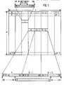
- a memory having p columns and m rows is accessed by word (or byte) addresses 0, l, 2, ... ; p, ... 2P-l, ... L, ... K, K+l, K+2, ... (mp-l). If a word consists of l6 bits, information of l6 bits is simultaneously read out of or written into the memory by one of the word addresses. It is assumed in this embodiment that one word consists of l6 bits.
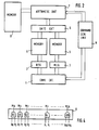
- Fig. 2 shows a block diagram of an information processing apparatus according to an embodiment of the present invention.
- the apparatus contains a control circuit l, two registers 2 and 3 coupled to the control circuit l, two memories 4 and 5 coupled to the registers 2 and 3, respectively, a gate circuit 6 coupled to output terminals of the memories 4 and 5, an arithmetic unit 7 coupled to the gate circuit 6, a command generating unit 8 coupled to the arithmetic unit 7 and the control circuit l, and a memory 9 shown in Fig. l.
- the control circuit l, the registers 2 and 3, the memories 4 and 5, and the gate circuit 6 are provided to produce the mask signal and the non-mask signal at the same time.
- the memory 4 stores a table shown in Fig. 3A and outputs l6-bit mask control signals X0 to X15 in response to any one of l6 addresses (0 to F).
- the memory 5 also stores a table shown in Fig. 3B and outputs l6-bit mask control signals Y0 to Y15 in response to an input data which is any one of l6 addresses (0 to F).
- the addresses 0 to F in Figs. 3A and 3B are represented by a hexadecimal digit.
- the bit numbers of the mask control signals X0 to X15 and Y0 to Y15 are the same and equal to the bit number of one word (l6 bits in this embodiment).
- addresses of the memories 4 and 5 are also equal to the bits of one word in number.
- a start bit address designating a bit position from which a processing is to start is applied to the memory 4, while an end bit address designating a bit position at which the processing is to terminate is applied to the memory 5.
- the end bit address to be applied to the memory 5 is F (l5) for the latter word and is calculated by using a bit length of bits to be processed for the former word as described hereinafter.
- "l" represents a non-mask control signal
- "0" represents a mask control signal.
- the memory 4 stores l6 first data, each representing the start bit position, and the memory 5 stores l6 second data, each representing the end bit position.
- the output signals of the memories 4 and 5 are applied to the gate circuit 6 (Fig. 2) which produces a mask signal and a non-mask signal.
- the gate circuit 6 may be formed by l6 AND gates (G0 to Gl5) as shown in Fig. 4, each of the AND gates receives the output signal X i for a word from the memory 4 and the output signal Y i for the same word from the memory 5.
- l the non-mask signal
- the remaining AND gate or gates produce the mask signal ("0"), so that l6-bit mask control signal is generated for one word.
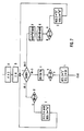
- Fig. 5 shows a block diagram of the control circuit l having a register (dAD) l0 storing a bit address, a register (DH) storing a value representing a bit length to be processed, a selector l2, a comparator l3, multiplexers l4, l6 and l8, an arithmetic logic circuit l6 and a register l7.
- the control circuit l produces a first data representing a start bit position of a data to be processed and a second data representing an end bit position of the data to be processed.
- the first data and the second data are stored in the registers 2 and 3 of Fig. 2, respectively, as addresses to be applied to the memories 4 and 5.
- the control circuit l produces these first data and second data according to the bit address representing the start bit position and the bit length of the data to be processed, which are sent from the command generating unit 8.
- the arithmetic unit 7 is coupled to the gate circuit 6, the memory 9 and the command generating unit 8 and performs an arithmetic operation commanded by the unit 8 for the data read out of the memory 9 by using the mask signal and the non-mask signal outputted from the gate circuit 6.
- a central processing unit CPU
- CPU central processing unit
- a program memory and a decoder or sequencer are used as the command generating unit 8.
- the memory 4 outputs a first data (00llllllllllllll) as X0 to X15 therefrom in response to the content (the start address "2") of the register 2. While the memory 5 outputs a second data (llllllllll000000) as Y0 to Y15 therefrom in response to a content (the end address "9") of the register 3.
- 00llllllll000000 are produced by the gate circuit 6 as M0 to M15.
- "0" represents a mask signal
- "l” represents a non-mask signal.
- P2 to P9 are selected among the l6-bit data of the word L as bits to be processed, and the remaining bits (P0, Pl and Pl0 to Pl5) are masked in the arithmetic unit 7.
- arbitrary bit or bits can be masked at a high speed by applying the start address and the end address to the registers 2 and 3, respectively.
- the present invention can be applied to mask arbitrary bit or bits from among a plurality of successive words. For example, in Fig. l A9 in a first word K to C3 in a third word K+2 can be selected at a high speed by the present invention. In this case, successive three word addresses K, K+l and K+2 are sequentially applied to the memory 9. The mask operation will be described with reference to Figs. l - 5 and 7 and 8.
- the start bit A9 of the bits to be processed is indicated by the word address K and the bit address "9". While, the end bit C3 is indicated by the word address K+2 and the bit address "3".
- the command generating circuit 8 sends the start bit address (dAD) "9” to the register l0 of the control circuit l and sends the value "26" representing a bit length (DH) to be processed to the register ll, respectively (STEPS A and B).
- the control circuit l compares a content of the register ll with a value "l6" by the comparator l3 because one word consists of l6 bits (STEPS C and D).
- the content of the register ll is larger than "l6" in this case, the content "9" of the register l0 is applied to the register 2 via the selector l2.
- the value "l5" is selected by the selector l2 and is applied to the register 3 as the end bit address of that word (STEP E).
- 0000 0000 0lll llll is read out of the memory 4 as the output X0 to X15, while llll llll llllll llllllll is read out of the memory 5 as the output Y0 to Y15.
- 000000000lllllll is outputted from the gate circuit 6, in which "0" represents a mask signal and "l” represents a non-mask signal.
- A9 to Al5 are selected from l6-bit data A0 - Al5 of the word K by the non-mask signal "l”, and A0 to A8 are masked by the mask signal "0".
- l6-bit data B0 to Bl5 of the successive word K+l is read out of the memory 9.
- the content of the register (dAD) l0 is subtracted from the value "l6" by the ALU l6 in a STEP F.
- the result is stored in the register l7.
- the content "26" of the register ll is applied via multiplexer l4 to the ALU l6.
- the content "7" of the register l7 is also applied via the multiplexer l5 to the ALU l6.
- the mask signal and the non-mask signal can be produced by a table access operation at a high speed. Particularly, they can be produced bit by bit without shifting operation. Further, since the arithmetic unit 7 does not participate the mask signal producing operation, it can execute the arithmetic operation in parallel with the mask signal producing operation.
- the command generating circuit 8 may directly apply the start bit and the end bit to the registers 2 and 3, respectively, without using the control circuit l. Further, when the same address is applied to the memories 4 and 5, all other bits except for only one bit are masked. On the other hand, when an address larger than that applied to the memory 5 is applied to the memory 4, all bits can be masked, and therefore, no operation (NOP) or a skip operation can be performed by using this mask operation. Further, a random logic circuit (e.g. a PLA circuit, an encoder circuit) may be used as the memories 4 and 5 to produce mask control signals as shown in Figs. 3A and 3B.
- a random logic circuit e.g. a PLA circuit, an encoder circuit
Abstract
Description
- The present invention relates to an information processing apparatus having a mask function, and particularly to an information processing apparatus having a mask function for masking an undesired bit or bits from among a plurality of bits read out of a memory.
- An information processing apparatus, in general, manipulates a plurality of bits altogether as the unit of processing which is defined as a byte or a word. For example, an 8-bit processor accesses a memory byte by byte, i.e., 8 bits by 8 bits, using an 8-bit data bus. In a l6-bit processor, l6 bits (two bytes = one word) are simultaneously manipulated.
- However, there is a case that only a part of bits of a byte or a word are required in order to execute a desired instruction. In this case, a bit or bits to be processed must be selected from among a plurality of bits. Heretofore, this was done by a bit-shift operation. However, the bit-shift operation requires a long period of time because the non-selected bit or bits also have to be shifted bit by bit. On the other hand, a mask operation has been proposed to select a part of the bits constituting a word or a byte. On the mask operation, non-selected bit or bits are masked by using a mask signal, and only a desired bit or bits are allowed to be taken out as valid bits. However, the mask operation of the prior art has produced the mask signal by combining a plurality of arithmetic instructions, so that complex processing and control are necessary. For instance, in order to detect a position of a bit to be masked a complex arithmetic calculation is required. When a plurality of bits are to be masked, the mask operation of the prior art requires a long period of time.
- It is therefore an object of the present invention to provide an information processing apparatus which can perform a mask operation at a high speed not only for a single bit but for a plurality of bits.
- An information processing apparatus of the present invention contains a first means for storing a first data indicating a start bit position of a start bit from which a processing is performed, a second means for storing a second data indicating an end bit position of an end bit at which the processing is terminated, and a third means coupled to the first means and the second means for producing a mask signal according to the first data and the second data.
- The first data and the second data consists of N bits, respectively. In the first data, each bit from a first bit to a bit just before the start bit has a first level signal, and each of the remaining bits, that is the start bit and the succeeding bit or bits, has a second level signal. While, in the second data, each of a first bit to the end bit has the second level signal, and the remaining bit or bits have the first level signal. The third means compares the first data with the second data bit by bit and produces a non-mask signal for each bit in which both the first data and the second data have the second level signals and produces a mask signal for each of the remaining bits. Thus, only the start bit to the end bit are not masked, while the remaining bit or bits are wholly masked. The third means has, for example, N gate circuits, each of which receives a bit of the first data and the corresponding bit of the second data, and produces N signals containing the mask signal and the non-mask signal. Here, one word or one byte is defined as consisting of N bits. The first means and the second means have a table of N × N bits, respectively, as described hereinafter.
- According to the present invention, the mask signal and the non-mask signal are produced at a high speed without using the bit-shift operation and the complex arithmetic operation. Particularly, mask signals for a plurality of bits can be produced at a high speed by the present invention, and therefore the present invention is suitable for an information processing apparatus in which each instruction is executed byte by byte or word by word.
-
- Fig. l is a diagram showing a memory map and a format of a data to be processed;
- Fig. 2 is a block diagram showing an information processing apparatus of an embodiment according to the present invention;
- Figs. 3A and 3B are tables of generating
circuits - Fig. 4 is a circuit diagram of a
gate circuit 6; - Fig. 5 is a circuit diagram of a control circuit l;
- Fig. 6 is a diagram showing outputs of the
memories gate circuit 6; - Fig. 7 is a flow chart showing an example of a mask operation of the present invention; and
- Fig. 8 is a diagram showing outputs of the
generating circuits gate circuit 6, respectively. - As shown in Fig. l, a memory having p columns and m rows is accessed by word (or byte)
addresses 0, l, 2, ... ; p, ... 2P-l, ... L, ... K, K+l, K+2, ... (mp-l). If a word consists of l6 bits, information of l6 bits is simultaneously read out of or written into the memory by one of the word addresses. It is assumed in this embodiment that one word consists of l6 bits. - When 8 bits P2 to P9 among l6 bits P0 to Pl5 of a word L are required in an arithmetic operation, P0, Pl and Pl0 to Pl5 must be masked.
- Fig. 2 shows a block diagram of an information processing apparatus according to an embodiment of the present invention. The apparatus contains a control circuit l, two
registers memories registers gate circuit 6 coupled to output terminals of thememories arithmetic unit 7 coupled to thegate circuit 6, acommand generating unit 8 coupled to thearithmetic unit 7 and the control circuit l, and amemory 9 shown in Fig. l. In this embodiment, the control circuit l, theregisters memories gate circuit 6 are provided to produce the mask signal and the non-mask signal at the same time. - The memory 4 (ROM) stores a table shown in Fig. 3A and outputs l6-bit mask control signals X₀ to X₁₅ in response to any one of l6 addresses (0 to F). The memory 5 (ROM) also stores a table shown in Fig. 3B and outputs l6-bit mask control signals Y₀ to Y₁₅ in response to an input data which is any one of l6 addresses (0 to F). The
addresses 0 to F in Figs. 3A and 3B are represented by a hexadecimal digit. The bit numbers of the mask control signals X₀ to X₁₅ and Y₀ to Y₁₅ are the same and equal to the bit number of one word (l6 bits in this embodiment). Further, addresses of thememories memory 4, while an end bit address designating a bit position at which the processing is to terminate is applied to thememory 5. When a word containing the end bit position is different from a word having the start bit position, the end bit address to be applied to thememory 5 is F (l5) for the latter word and is calculated by using a bit length of bits to be processed for the former word as described hereinafter. In Figs. 3A and 3B, "l" represents a non-mask control signal, while "0" represents a mask control signal. - In the
memory 4, "0" is stored from a first location X₀ to a location just before a location corresponding to the start bit position, and "l" is stored from the location corresponding to the start bit position to a last location X₁₅. In thememory 5, "l" is stored from a first location Y₀ to a location corresponding to the end bit position, and "0" is stored from a location subsequent to the location corresponding to the end bit position to a last location Y₁₅. Thus, thememory 4 stores l6 first data, each representing the start bit position, and thememory 5 stores l6 second data, each representing the end bit position. - The output signals of the
memories gate circuit 6 may be formed by l6 AND gates (G0 to Gl5) as shown in Fig. 4, each of the AND gates receives the output signal Xi for a word from thememory 4 and the output signal Yi for the same word from thememory 5. Thus, only the AND gate or gates which receive both "l" of the output signals Xi and Yi produce the non-mask signal ("l"), and the remaining AND gate or gates produce the mask signal ("0"), so that l6-bit mask control signal is generated for one word. - Fig. 5 shows a block diagram of the control circuit l having a register (dAD) l0 storing a bit address, a register (DH) storing a value representing a bit length to be processed, a selector l2, a comparator l3, multiplexers l4, l6 and l8, an arithmetic logic circuit l6 and a register l7. The control circuit l produces a first data representing a start bit position of a data to be processed and a second data representing an end bit position of the data to be processed. The first data and the second data are stored in the
registers memories command generating unit 8. - The
arithmetic unit 7 is coupled to thegate circuit 6, thememory 9 and thecommand generating unit 8 and performs an arithmetic operation commanded by theunit 8 for the data read out of thememory 9 by using the mask signal and the non-mask signal outputted from thegate circuit 6. A central processing unit (CPU) can be employed as thearithmetic unit 7, and a program memory and a decoder or sequencer are used as thecommand generating unit 8. - An operation for producing the mask signal and the non-mask signal will be explained with references to Figs. l to 6. An address of a start bit P2 to be processed for the word L is "2", while an address of an end bit P9 is "9". Therefore, the value "2" is set into the
register 2, while the value "9" is set into theregister 3. These values can be directly set into therespective registers - The
memory 4 outputs a first data (00llllllllllllll) as X₀ to X₁₅ therefrom in response to the content (the start address "2") of theregister 2. While thememory 5 outputs a second data (llllllllll000000) as Y₀ to Y₁₅ therefrom in response to a content (the end address "9") of theregister 3. These two data are applied to the gate circuit shown in Fig. 4, whereby 00llllllll000000 are produced by thegate circuit 6 as M₀ to M₁₅. Here, "0" represents a mask signal and "l" represents a non-mask signal. Thus, only P2 to P9 are selected among the l6-bit data of the word L as bits to be processed, and the remaining bits (P0, Pl and Pl0 to Pl5) are masked in thearithmetic unit 7. - According to the present invention, arbitrary bit or bits can be masked at a high speed by applying the start address and the end address to the
registers - The present invention can be applied to mask arbitrary bit or bits from among a plurality of successive words. For example, in Fig. l A9 in a first word K to C3 in a third word K+2 can be selected at a high speed by the present invention. In this case, successive three word addresses K, K+l and K+2 are sequentially applied to the
memory 9. The mask operation will be described with reference to Figs. l - 5 and 7 and 8. - The start bit A9 of the bits to be processed is indicated by the word address K and the bit address "9". While, the end bit C3 is indicated by the word address K+2 and the bit address "3". The
command generating circuit 8 sends the start bit address (dAD) "9" to the register l0 of the control circuit l and sends the value "26" representing a bit length (DH) to be processed to the register ll, respectively (STEPS A and B). The control circuit l compares a content of the register ll with a value "l6" by the comparator l3 because one word consists of l6 bits (STEPS C and D). Since the content of the register ll is larger than "l6" in this case, the content "9" of the register l0 is applied to theregister 2 via the selector l2. With respect to the word A0 to Al5, since A9 to Al5 are to be processed, the value "l5" is selected by the selector l2 and is applied to theregister 3 as the end bit address of that word (STEP E). At this time, 0000 0000 0lll llll is read out of thememory 4 as the output X₀ to X₁₅, while llll llll llll llll is read out of thememory 5 as the output Y₀ to Y₁₅. These outputs are ANDed by thegate circuit 6. As the result, 000000000lllllll is outputted from thegate circuit 6, in which "0" represents a mask signal and "l" represents a non-mask signal. Thus, A9 to Al5 are selected from l6-bit data A0 - Al5 of the word K by the non-mask signal "l", and A0 to A8 are masked by the mask signal "0". - Next, l6-bit data B0 to Bl5 of the successive word K+l is read out of the
memory 9. In order to detect the number of bits which have been processed in the first word (K), the content of the register (dAD) l0 is subtracted from the value "l6" by the ALU l6 in a STEP F. The result is stored in the register l7. Further, to correct the bit length to be processed, the content "26" of the register ll is applied via multiplexer l4 to the ALU l6. The content "7" of the register l7 is also applied via the multiplexer l5 to the ALU l6. In the ALU l6, subtraction of "26" minus "7" is executed, and the result "l9" is stored to the register ll via the multiplexer l8 (STEP G). Thereafter, the content "l9" of the register is compared with the value "l6" by the comparator l3 (STEP H). Since the content "l9" of the register ll is larger than "l6", the control unit l determines that all bits B0 to Bl5 of the second word (K+l) must be processed. Thus, the selector l2 applies "0" to theregister 2 as the start bit address and applied "l5(=F)" to theregister 2 as the end bit address, respectively (STEP I). Consequently, llll llll llll llll are read out of bothmemories gate circuit 6 produces llllllllllllllll (all non-mask signals) for the second word K+l. Thus, the l6 bits B0 to Bl5 of the word K+l are all processed by thearithmetic unit 7. - In a STEP J, to produce a mask signal for the third word K+2 (l6-bit data C0 to Cl5) read out of the
memory 9, the content of the register (DH) ll is subtracted by the value "l6" which is the number of bits to be processed for the second word K+l. The result is "3" which is smaller than the value "l6". Therefore, "0" is sent to theregister 2 as the start bit of the third word, and "3" is sent to theregister 3 as the end address of the third word. Thus, llll llll llll llll is read out of thememory 4, andllll 0000 0000 0000 is read out of thememory 5, whereby thegate circuit 6 produces an output signal llll000000000000. As a result, first 4 bits C0 to C3 are not masked for the thirdword K+ 2, while the remaining l2 bits C4 to Cl5 are masked. - As described above, the mask signal and the non-mask signal can be produced by a table access operation at a high speed. Particularly, they can be produced bit by bit without shifting operation. Further, since the
arithmetic unit 7 does not participate the mask signal producing operation, it can execute the arithmetic operation in parallel with the mask signal producing operation. - In the present invention, when a word contains both the start bit and the end bit as shown in the word L, the
command generating circuit 8 may directly apply the start bit and the end bit to theregisters memories memory 5 is applied to thememory 4, all bits can be masked, and therefore, no operation (NOP) or a skip operation can be performed by using this mask operation. Further, a random logic circuit (e.g. a PLA circuit, an encoder circuit) may be used as thememories
Claims (10)
Applications Claiming Priority (2)
| Application Number | Priority Date | Filing Date | Title |
|---|---|---|---|
| JP81709/86 | 1986-04-08 | ||
| JP61081709A JPS62237522A (en) | 1986-04-08 | 1986-04-08 | Information processor |
Publications (2)
| Publication Number | Publication Date |
|---|---|
| EP0241001A2 true EP0241001A2 (en) | 1987-10-14 |
| EP0241001A3 EP0241001A3 (en) | 1990-07-11 |
Family
ID=13753914
Family Applications (1)
| Application Number | Title | Priority Date | Filing Date |
|---|---|---|---|
| EP87105153A Withdrawn EP0241001A3 (en) | 1986-04-08 | 1987-04-07 | Information processing apparatus having a mask function |
Country Status (3)
| Country | Link |
|---|---|
| US (1) | US4870563A (en) |
| EP (1) | EP0241001A3 (en) |
| JP (1) | JPS62237522A (en) |
Cited By (1)
| Publication number | Priority date | Publication date | Assignee | Title |
|---|---|---|---|---|
| WO1990002373A1 (en) * | 1988-08-30 | 1990-03-08 | Unisys Corporation | Merge select decode checking |
Families Citing this family (11)
| Publication number | Priority date | Publication date | Assignee | Title |
|---|---|---|---|---|
| US5148523A (en) * | 1988-11-29 | 1992-09-15 | Solbourne Computer, Inc. | Dynamic video RAM incorporationg on chip line modification |
| US5142637A (en) * | 1988-11-29 | 1992-08-25 | Solbourne Computer, Inc. | Dynamic video RAM incorporating single clock random port control |
| USRE35680E (en) * | 1988-11-29 | 1997-12-02 | Matsushita Electric Industrial Co., Ltd. | Dynamic video RAM incorporating on chip vector/image mode line modification |
| US5148524A (en) * | 1988-11-29 | 1992-09-15 | Solbourne Computer, Inc. | Dynamic video RAM incorporating on chip vector/image mode line modification |
| KR930008042B1 (en) * | 1991-04-03 | 1993-08-25 | 삼성전자 주식회사 | Microcontroller unit |
| US5598514A (en) * | 1993-08-09 | 1997-01-28 | C-Cube Microsystems | Structure and method for a multistandard video encoder/decoder |
| US5910909A (en) * | 1995-08-28 | 1999-06-08 | C-Cube Microsystems, Inc. | Non-linear digital filters for interlaced video signals and method thereof |
| US5826071A (en) * | 1995-08-31 | 1998-10-20 | Advanced Micro Devices, Inc. | Parallel mask decoder and method for generating said mask |
| US5745744A (en) * | 1995-10-12 | 1998-04-28 | International Business Machines Corporation | High speed mask generation using selection logic |
| US7529907B2 (en) * | 1998-12-16 | 2009-05-05 | Mips Technologies, Inc. | Method and apparatus for improved computer load and store operations |
| US6738792B1 (en) | 2001-03-09 | 2004-05-18 | Advanced Micro Devices, Inc. | Parallel mask generator |
Citations (4)
| Publication number | Priority date | Publication date | Assignee | Title |
|---|---|---|---|---|
| US3370274A (en) * | 1964-12-30 | 1968-02-20 | Bell Telephone Labor Inc | Data processor control utilizing tandem signal operations |
| DE2233164A1 (en) * | 1972-07-06 | 1974-01-24 | Licentia Gmbh | CIRCUIT ARRANGEMENT FOR HIDING ANY SELECTABLE AREA OF A BIT SEQUENCE WHEN TRANSFERRED BETWEEN TWO REGISTERS |
| US4012722A (en) * | 1975-09-20 | 1977-03-15 | Burroughs Corporation | High speed modular mask generator |
| JPS5875235A (en) * | 1981-10-27 | 1983-05-06 | Omron Tateisi Electronics Co | Operation input processor |
Family Cites Families (7)
| Publication number | Priority date | Publication date | Assignee | Title |
|---|---|---|---|---|
| US3366927A (en) * | 1964-06-17 | 1968-01-30 | Ibm | Computing techniques |
| US3665175A (en) * | 1968-09-03 | 1972-05-23 | Ibm | Dynamic storage address blocking to achieve error toleration in the addressing circuitry |
| GB1378143A (en) * | 1971-07-23 | 1974-12-18 | Int Computers Ltd | Data processors |
| US3786434A (en) * | 1972-12-20 | 1974-01-15 | Ibm | Full capacity small size microprogrammed control unit |
| US3949370A (en) * | 1974-06-06 | 1976-04-06 | National Semiconductor Corporation | Programmable logic array control section for data processing system |
| JPS5115381U (en) * | 1974-07-19 | 1976-02-04 | ||
| US4713751A (en) * | 1984-10-24 | 1987-12-15 | International Business Machines Corporation | Masking commands for a second processor when a first processor requires a flushing operation in a multiprocessor system |
-
1986
- 1986-04-08 JP JP61081709A patent/JPS62237522A/en active Pending
-
1987
- 1987-04-07 EP EP87105153A patent/EP0241001A3/en not_active Withdrawn
- 1987-04-08 US US07/036,754 patent/US4870563A/en not_active Expired - Lifetime
Patent Citations (4)
| Publication number | Priority date | Publication date | Assignee | Title |
|---|---|---|---|---|
| US3370274A (en) * | 1964-12-30 | 1968-02-20 | Bell Telephone Labor Inc | Data processor control utilizing tandem signal operations |
| DE2233164A1 (en) * | 1972-07-06 | 1974-01-24 | Licentia Gmbh | CIRCUIT ARRANGEMENT FOR HIDING ANY SELECTABLE AREA OF A BIT SEQUENCE WHEN TRANSFERRED BETWEEN TWO REGISTERS |
| US4012722A (en) * | 1975-09-20 | 1977-03-15 | Burroughs Corporation | High speed modular mask generator |
| JPS5875235A (en) * | 1981-10-27 | 1983-05-06 | Omron Tateisi Electronics Co | Operation input processor |
Non-Patent Citations (2)
| Title |
|---|
| IBM TECHNICAL DISCLOSURE BULLETIN, vol. 27, no. 10A, March 1985, pages 5696-5698, New York, US; Mask Generator for 32-bit Microprocessors" * |
| PATENT ABSTRACTS OF JAPAN, vol. 7, no. 168 (P-212)[1313], 23rd July 1983; & JP-A-58 75 235 (TATEISHI DENKI K.K.) 06-05-1983 * |
Cited By (1)
| Publication number | Priority date | Publication date | Assignee | Title |
|---|---|---|---|---|
| WO1990002373A1 (en) * | 1988-08-30 | 1990-03-08 | Unisys Corporation | Merge select decode checking |
Also Published As
| Publication number | Publication date |
|---|---|
| US4870563A (en) | 1989-09-26 |
| JPS62237522A (en) | 1987-10-17 |
| EP0241001A3 (en) | 1990-07-11 |
Similar Documents
| Publication | Publication Date | Title |
|---|---|---|
| US4400697A (en) | Method of line buffer loading for a symbol generator | |
| EP0050406A1 (en) | Conditional branch prediction apparatus and method | |
| EP0241001A2 (en) | Information processing apparatus having a mask function | |
| US4141268A (en) | Keyboard apparatus for an electronic musical instrument | |
| EP0248235B1 (en) | Image processing apparatus having function of enlargement and/or shrinkage of image | |
| US4429414A (en) | Pattern recognition system operating by the multiple similarity method | |
| EP0206504A2 (en) | Search apparatus | |
| US3969704A (en) | Word transformation apparatus for digital information processing | |
| GB2110856A (en) | Range recognizer | |
| EP0280320B1 (en) | Graphics display controller equipped with boundary searching circuit | |
| US6424958B1 (en) | Coding and storing method for fuzzy logic rules and circuit architecture for processing such rules | |
| CN87103852A (en) | Partial write control apparatus | |
| US4162519A (en) | Data processor with address allocation to operations | |
| US5117487A (en) | Method for accessing microprocessor and microinstruction control type microprocessor including pointer register | |
| US4812970A (en) | Microprogram control system | |
| US4899128A (en) | Method and apparatus for comparing strings using hash values | |
| US5504871A (en) | Memory controller having bus master for addressing instruction memories | |
| US4453227A (en) | Method and apparatus for transferring a bit pattern field into a memory | |
| US5465225A (en) | Method of increasing the data-processing speed of a signal processor | |
| US4404629A (en) | Data processing system with latch for sharing instruction fields | |
| US5854919A (en) | Processor and its operation processing method for processing operation having bit width exceeding data width of bit storage unit | |
| JPS6318222B2 (en) | ||
| GB2169118A (en) | Digit strobe designation | |
| JPS6168636A (en) | Data processor | |
| SU1161943A1 (en) | Microcommand memory control unit |
Legal Events
| Date | Code | Title | Description |
|---|---|---|---|
| PUAI | Public reference made under article 153(3) epc to a published international application that has entered the european phase |
Free format text: ORIGINAL CODE: 0009012 |
|
| 17P | Request for examination filed |
Effective date: 19870407 |
|
| AK | Designated contracting states |
Kind code of ref document: A2 Designated state(s): DE FR GB |
|
| PUAL | Search report despatched |
Free format text: ORIGINAL CODE: 0009013 |
|
| AK | Designated contracting states |
Kind code of ref document: A3 Designated state(s): DE FR GB |
|
| 17Q | First examination report despatched |
Effective date: 19920128 |
|
| STAA | Information on the status of an ep patent application or granted ep patent |
Free format text: STATUS: THE APPLICATION HAS BEEN WITHDRAWN |
|
| 18W | Application withdrawn |
Withdrawal date: 19920714 |
|
| RIN1 | Information on inventor provided before grant (corrected) |
Inventor name: OGUCHI, TETSUJIC/O NEC CORPORATION |