EP0241403A1 - Bidirectional motor drive circuit - Google Patents
Bidirectional motor drive circuit Download PDFInfo
- Publication number
- EP0241403A1 EP0241403A1 EP87630023A EP87630023A EP0241403A1 EP 0241403 A1 EP0241403 A1 EP 0241403A1 EP 87630023 A EP87630023 A EP 87630023A EP 87630023 A EP87630023 A EP 87630023A EP 0241403 A1 EP0241403 A1 EP 0241403A1
- Authority
- EP
- European Patent Office
- Prior art keywords
- motor
- power mosfets
- low
- drive circuitry
- control
- Prior art date
- Legal status (The legal status is an assumption and is not a legal conclusion. Google has not performed a legal analysis and makes no representation as to the accuracy of the status listed.)
- Granted
Links
Images


Classifications
-
- H—ELECTRICITY
- H02—GENERATION; CONVERSION OR DISTRIBUTION OF ELECTRIC POWER
- H02P—CONTROL OR REGULATION OF ELECTRIC MOTORS, ELECTRIC GENERATORS OR DYNAMO-ELECTRIC CONVERTERS; CONTROLLING TRANSFORMERS, REACTORS OR CHOKE COILS
- H02P1/00—Arrangements for starting electric motors or dynamo-electric converters
-
- H—ELECTRICITY
- H02—GENERATION; CONVERSION OR DISTRIBUTION OF ELECTRIC POWER
- H02M—APPARATUS FOR CONVERSION BETWEEN AC AND AC, BETWEEN AC AND DC, OR BETWEEN DC AND DC, AND FOR USE WITH MAINS OR SIMILAR POWER SUPPLY SYSTEMS; CONVERSION OF DC OR AC INPUT POWER INTO SURGE OUTPUT POWER; CONTROL OR REGULATION THEREOF
- H02M1/00—Details of apparatus for conversion
- H02M1/38—Means for preventing simultaneous conduction of switches
-
- H—ELECTRICITY
- H02—GENERATION; CONVERSION OR DISTRIBUTION OF ELECTRIC POWER
- H02P—CONTROL OR REGULATION OF ELECTRIC MOTORS, ELECTRIC GENERATORS OR DYNAMO-ELECTRIC CONVERTERS; CONTROLLING TRANSFORMERS, REACTORS OR CHOKE COILS
- H02P7/00—Arrangements for regulating or controlling the speed or torque of electric DC motors
- H02P7/03—Arrangements for regulating or controlling the speed or torque of electric DC motors for controlling the direction of rotation of DC motors
- H02P7/04—Arrangements for regulating or controlling the speed or torque of electric DC motors for controlling the direction of rotation of DC motors by means of a H-bridge circuit
Definitions
- the present invention relates to the control of a motor and more particularly to an electronic control system for small bidirectional DC inductive motors.
- FIG. 1 A relatively traditional wiper system for the window of an automotive vehicle is depicted in Fig. 1 herein.
- That system includes a two-speed wiper motor 10, a cammed Run switch 112, a cammed Park switch 114, relatively conventional drive and control electronics 116 which employed bipolar transistors and electromechanical relays, several ganged high-current wiper mode switches, generally represented as 118 and a potentiometer 120 for adjusting the delay interval for intermittent operation.
- the cammed Run switch 112 carries the current of wiper motor 110 while the wiper, or wipers, represented by reference numeral 122 is sweeping across the windshield.
- the cammed Park switch 114 is used to reverse the direction of rotation of wiper motor 110 which in turn brings the wiper 122 to the "Depressed Park" position.
- the forward and return sweeping motion of the wiper 122 across a windshield is performed in the linkage between it and the wiper motor 110 such that the motor is normally only rotated in a single direction, but is reversed to move the wiper 122 into the "Depressed Park" position.
- Other wiper systems exist in which the linkage to the wipers and the control of the motor is such that the direction of rotation of the motor is reversed for the forward and return sweeping motion.
- U.S. Patent 4,454,454 to Valentine for MOSFET "H" SWITCH CIRCUIT FOR A DC MOTOR describes what is characterized as an "improved MOSFET'H switch circuit for a DC motor". That circuit employs four power MOSFETS connected in an "H" switch, or bridge, configuration for providing bidirectional control of a fractional horsepower DC motor, as for instance used to drive windshield wipers. That motor drive circuit is characterized as providing various advantages over the use of bipolar transistors for reversing the motor supply voltage for bidirectional control and/or for speed control of the motor. Indeed, the utilization of power MOSFETS in an H-bridge configuration does appear to provide advantages over the utilization of other types of switching devices. While that patent does disclose .
- an improved motor drive circuit for a bidirectional inductive DC motor, the motor having first and second terminals for operative connection with a source of DC electrical power and the drive circuitry being adapted to be connected in series with the motor terminals across the source of DC electrical power.
- the motor drive circuitry includes four power MOSFETS operatively connected to the motor terminals in H-bridge configuration across the power source, the four power MOSFETS including first and second high-side power MOSFETS operatively connected to the first and second motor terminals respectively, and first and second low-side powwer MOSFETS operatively connected to the first and second motor terminals respectively.
- the drive circuit further includes first and second input terminals and first and second intermediate switching circuitry.
- the input terminals receive respective control signals, each of which is one of two possible logic states.
- the first intermediate switching circuitry is operatively connected between the first input terminal'and the gates of the first high-side and first low-side power MOSFETS for controlling conduction of the first high-side and the first low-side power MOSFETS in a substantially complementary manner.
- the second intermediate switching circuitry is operatively connected between the second input terminal and the gates of the second high-side and second low-side power MOSFETS for controlling conduction of the second high-side and the second low-side power MOSFETS also in a substantially complementary manner.
- the first and second intermediate switching circuits each include a series pair of control MOSFETS which are connected between a respective input terminal and the gate of one of the respective high-side and low-side power MOSFETS. Further, one of the control MOSFETS of each pair is connected between the respective input terminal and the gate of the other of the respective high-side and low-side power MOSFETS.
- the respective control MOSFETS of the first and second intermediate switching circuits have predetermined maximum threshold voltages and the respective power MOSFETS have predetermined minimum threshold voltages which are higher than the maximum threshold voltages of the control MOSFETS such as to impede cross-conduction between respective high-side and low-side power MOSFETS.
- the power MOSFETS each include respective inherent input capacitances and the first and second intermediate switching circuits include respective resistances which are connected to the gates of the respective power MOSFETS and are configured and preselected to provide, in combination with the respective input capacitances, turn-on time constants which are longer than the corresponding turn-off time constants for the respective power MOSFETS thereby to further impede cross-conduction between respective high-side and and low-side power MOSFETS.
- the control signals received at the first and second input terminals may concurrently be of the same logic state, that state being operative to effect conduction of the first and second high side power MOSFETS or the first and second low-side power MO SF E TS concurrently for braking the motor.
- a third input terminal is also provided for receiving a pulse-width modulated control signal, and circuit means are provided for extending that pulse-width modulated control signal only to each of the first and second low-side power MOSFETS for controlling the speed of the motor.
- the circuitry which extends the pulse-width modulated control signals to the first and second low-side power MOSFETS operates to regulate the conduction only of that one of the first and second low-side power MOSFETS which has been rendered conductive by the control signals at the first and second input terminals.
- Speed control of the motor is provided by utilizing a pulse-width modulated control signal which has a relatively slow repetition rate in order to exploit the inductive characteristics of the motor in an optimal manner. That repetition rate is less than about 500 Hz and is preferably in the range of 30-75 Hz. Such relatively-slow repetition rate further enables a relativley-slow switching rate for the power MOSFETS to minimize the adverse effects of inductive transients.
- the duration of any "off" portion of the duty cycle of the pulse-width modulated control signal is made at least long enough that the body diodes inherent in each power MOSFET have time to recover. Further, assuming a transient protection circuit is included to prevent voltage transients greater than a predetermined amplitude from being passed to the drive circuitry, at least .
- the high-side power MOSFETS are selected to have a minimum breakdown voltage which is at least twice the amplitude of the transient protection.
- the motor drive circuitry of the present invention is particularly suited for use with automotive motors, as for instance window wiper motors.
- wiper control system As used herein when referring to the wiper control system and its mode of operation, the following terms are synonymous and may be used interchangeably: “sweep” with “stroke”; “forward/reverse” with “forward/return”; “inner reversing position” with “parking position”; “FET” with “MOSFET”; “cammed run switch” with “Run cam”; “on” with “conducting”; and “off” with “nonconducting”.
- the multiplex control system includes a central microcomputer 10, a master multiplex device, Master Mux 11, and a plurality of slave-type multiplex devices, Remuxes 12.
- the central microcomputer 10 includes a memory capacity, both ROM and RAM, for storing data and appropriate operating and control programming.
- the Master Mux 11 transmits and receives data, respectively, to and and from the Remuxes 12.
- the Remuxes 12 serve as input and/or output interfacing devices.
- a four-wire multiplex bus 14 provides +5 volt and ground potentials as well as a DATA line and a CLOCK line.
- the multiplex CLOCK frequency is, for example, 25 KHz.
- switches 16, 17 and 18 selectively provide inputs to one of the Remuxes 12 for commanding various functional responses of the wiper system.
- Switch 16 controls Intermittent Clear and OFF control
- switch 17 controls low/high operation
- switch 18 may control a wash pump motor and associated wash cycle, not shown.
- one, or more typically two, windshield wipers 20 are driven across a windshield 19 by a permanent magnet motor 22 via connecting linkage 24 by control circuitry structured in accordance with the invention.
- input switch 17 will initiate operation of wiper motor 22.
- the control of motor 22 is effected via a control program stored in microcomputer 10 and transmitted to the motor 22 via one of the Remuxes 12 and wiper power drive circuitry 26.
- the Remux 12 which serves as an interface between the wiper power drive circuitry 26 and the multiplex bus 14, has the capability of providing certain control signals as logic levels on various outputs thereof. It additionally is capable of converting appropriate data from central microcomputer 10 to a pulse-width modulated (PWM) control signal on yet another output, in a manner described in detail in the aforementioned Application Serial No. 664,804. Still further, that Remux 12 is capable of receiving input signals, as for instance, the feedback signal appearing on lead 27.
- PWM pulse-width modulated
- the wiper drive circuitry 26 may be provided with appropriate - transient protection circuitry 30 between it and the 12 volt DC source for protection from external transients.
- a charge pump 32 is provided for certain of the circuit elements in the wiper power drive circuitry 26 to be hereinafter described.
- a cammed Run switch 34 of conventional design provides a signal which indicates a reference position of the wipers 20, 20'.
- windshield wipers 20, 20' of Fig. 2 are depicted as being a pair of wipers connected and driven by a common linkage, it will be understood that the invention is similarly applicable to a single wiper.
- FIG. 3 the stroke or sweep pattern of a single wiper blade is depicted as appearing on a windshield 19.
- a normal wiping cycle comprises a Forward stroke and Return stroke, with the Forward stroke beginning at an Inner Reversing Position and the Return stroke beginning at an Outer Reversing Position.
- a third position, designated Depressed Park, represents a common option for storing the wipers out of sight when not in use.
- the power drive circuitry 26 operates in conjunction with Control 41, Control #2 and PWM Control signals from Remux 12 to regulate the supply of electrical power from the 12 volt source to the motor 22.
- wiper motor 22 may be of a conventional design having an armature with a common (C) terminal at one end and low (L) and high (H) terminals spaced therealong for low and high speed operation, respectively.
- C common
- L low
- H high
- the low speed terminal (L) has only been shown by dotted line inasmuch it is not used in the present example.
- the power regulating circuitry 26 responds to the control signals t1 and #2 for determing the direction in which motor 22 rotates.
- the motor 22 only rotates in a single direction during normal Run operation and known structuring of the linkage 24 acts to provide the sweep-reversing function which provides both the Forward and Return strokes.
- Motor 22 may be reversed by appropriate control of control signals #1 and #2 if it is desired to move the wipers 20, 20' into a depressed park position.
- the PWM Control signal regulates the supply of power to the wiper motor 22 in a manner which regulates the speed of the motor.
- the PWM Control signal is a two-state (logic 1,0) variable duty cycle control signal having a repetition rate of approximately 50 Hz and being incrementable in 32 steps between zero percent duty cycle and 100% duty cycle.
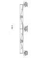
- the power regulating circuitry 26 of the invention is depicted in greater detail.
- the windshield wiper motor in this figure has been designated 22' to identify that it does not include a third terminal, i.e. low speed terminal L.
- its two terminals have been designated C and H' to indicate that it has the capacity for a greater speed than the C, H terminals of motor 22 of Fig. 2. This capability is necessitated if it is desired to provide the same maximum speed capability of motor 22, yet provide the speed regulation characteristics of the invention.
- the power regulating circuitry 26 of Fig. 4 provides one or more power MOSFETS connected in series with the motor and across the 12 volt DC supply for regulating the flow of current, and thus power, to the motor.
- a single power MOSFET in series with the motor 22' and having its periods of conduction controlled by the PWM Control signal to provide speed regulation.
- most practical windshield wiper systems require bidirectional control of the motor 22' to permit attaining the Depressed Park position. Therefore, it is preferable to provide four power MOSFETS arranged in a so-called "H-bridge" configuration for bidirectionally controlling the flow of current through the motor.
- the four power MOSFETS are designated 40a, 40b, 40c and 40d, with MOSFETS 40a and 40b being connected to the C terminal of motor 22' and MOSFETS 40c and 40d being connected to the H' terminal.
- the power MOSFETS 40a-d are N-channel devices, such as Z30's of International Rectifier. They are of relatively low cost and can carry the stall current of motor 22'.
- a charge pump 32 seen in Fig. 2, provides a V.Pump supply at about 10 volts above the +12V power source supply, for the high-side, N-Channel power MOSFETS 40a and 40c, as well as for other similar devices in the Remux 12. Conduction by power MOSFETS 40a and 40d provides a current path in one direction through motor 22' for one direction of rotation, and conduction by power MOSFETS 40c and 40b provides a current path in the opposite direction through the motor for reverse rotation.
- two control MOSFETS 42 and 44 are operatively connected in series between the input for the Control #1 signal and the gate of power FET 40 in a manner which turns that power FET “ON” when the Control #1 signal is at a logic 1.
- Two similar control FETS 46 and 48 are operatively connected in series between the input for the Control #2 signal and the gate of power FET 40c in a manner which turns that power FET “ON” when the Control #2 signal is a logic 1.
- a logic 0 at Control #1 or Control #2 input turns the respective power FET "OFF”.
- a logic 1 at the Control #1 or Control #2 input turns the respective high-side power -FET 40a or 40c "ON", it is operatively connected to the gate of the respective associated low-side power FET 40b or 40d in a manner which serves to turn that device "OFF".
- a logic 1 on one of the Control #1 or Control #2 inputs and a logic 0 on the other of those inputs serves to turn “ON” a pair of power FETS which are connected in series with the motor 22', for instance 40b and 40c. Reversal of that logic signal pattern results in conduction in the opposite direction through the other pair of power FETS.
- the PWM Control signal is extended via a further control MOSFET 50 and diodes 52b and 52d to the gates of respective power FETS 40b and 40d for turning that conducting power FET alternately “ON” and “OFF” in accordance with the duty cycle of the PWM control signal.
- This PWM Control signal is prevented from turning the presently nonconducting, low-side power FET “ON” by the diodes 54b and 54d in order to prevent a shorted connection through two power FETS connected to the same terminal of the motor.
- Fig. 4A there is depicted a functional equivalent diagram of the power feed lines, the wiper power drive circuitry 26 and the wiper motor 22'.
- the battery, BATT provides the nominal 12 volt supply.
- the feed line from the positive terminal of the battery to the power drive circuitry 26 includes a lumped resistance RFEED and a lumped inductance L FEED .
- the return lead extending from the power drive circuitry 26 to the negative terminal of the battery includes a lumped resistance, R RETURN' and a lumped inductance, L RETURN"
- Each of the power MOSFETS 40a-d has been represented by a simple mechanical switch in an open or closed state and includes the reverse body diode normally associated with this type of power MOSFET.
- the conductive path through the motor is presumed to occur through conducting, high-side power FET 40c and -the PWM controlled low-side power FET 40b.
- Power FETS 40a and 40d are presumed to be nonconducting.
- the voltages across R FEED and R RETURN are presumed to be negligible.
- MOSFET 40b As MOSFET 40b is opened, or becomes nonconductive, two events occur. Firstly, the current IF from the battery goes to zero at a rate of dI F/ dt which is proportional to the switching speed of the power MOSFET. A relatively slow PWM rate will allow relatively slow switching rates for the power MOSFETS and thus low dI F/ dt. By further subdividing one period of the PWM Control signal into 32 parts, it is possible to get the requisite speed control without accelerating the switching times of the various power FETS. A voltage will be generated across the L FEED and L RETURN inductances of a value:
- the wiper motor 22' is also of an inductive nature and stores a sizable amount of energy when current is flowing through it.
- MOSFET 40b When MOSFET 40b is opened, the voltage to power MOSFETS 40a and 40b from the motor will rise due to:
- the design of the present circuitry ensures that the lower power FET 40b is not turned back on until the inductive energy of the motor is dissipated, otherwise secondary breakdown and resultant overheating and current "hogging" may occur. Further, the ratings of the power FETS are selected to be at least-twice the voltage that can appear between V FEED and V RETURN .
- the power FETS are sized for twice the value of any protection provided for transients.
- Speed control using PWM is more efficient if the motor is allowed to generate instead of being braked during the "OFF" portion of each duty cycle.
- the power dissipated in both the motor 22' and the drive circuitry 26 is minimized by coasting rather than braking during the speed control. This is because braking doesn't allow the inductive energy to circulate and because it depletes the kinetic energy of the moving motor elements. However, braking may be desirable and is provided in those instances when it is desired to quickly stop the motor 22' at a_precise position, as for intermittent operation or when terminating operation. Braking is provided by applying the same logic value at both the Control #1 and #2 inputs such that either both high-side power MOSFETS 40a and 40c or both low-side power MOSFETS 40b and 40d conduct and provide a short across motor 22'.
- a PWM Control signal which has a repetition rate which is relatively slow.
- a PWM Control repetition rate which is below about 500 Hz and preferably is in the range of 30-75 Hz is much more controllable than significantly higher rates.
- the efficiency may stay about the same, if switching losses are neglected, but controllability decreases. This effect is due to the inductive nature of the permanent magnet wiper motor 22'.
- wiper motors as used in the H-bridge, nonbraked (coasting) configuration of the present invention have inductive energy time constants in the range of 1-2 milliseconds.
- the kinetic energy of motor 22' which takes hundreds of milliseconds to be dissipated, is utilized during the "OFF" portion of the PWM duty cycle to maintain the motion of the motor.
- the supply current and the motor current during the "ON" portion of the PWM period are greater than for the situation of a substantially higher PWM repetition rate.
- the kinetic energy decay rate for a typical system employing the circuitry of the invention and operating at a conventional "low" wiper speed is hundreds of milliseconds which allows pulse-width modulation. rates as low as 30 Hz with essentially no "cogging" effects. It has been noted that operation at this PWM repetition rate is acoustically about the same as a traditional system operating at "low” speed.
- Control #2 signal is changed from a logic 0 (0V) to a logic 1 (5V)
- control FET 46 turns “ON” and decreases the voltage on the gates of control FET 48 and power FET 40d. Since the minimum “ON” threshold of power FET 40d is above the maximum “ON” threshold of control FET 48, power FET 40d will turn “OFF” before control FET 48 turns “OFF”. Power FET 40c cannot turn “ON” until control FET 48 turns “OFF”. Thus, there is no overlap of the power FETS 40c and 40d in the "ON” condition.
- Control #2 signal then changes to a logic 0, as that occurs the control FET 46 turns “OFF” and the voltage to the gate of control FET 48 and power FET 40d rises. Since the maximum “ON” threshold of control FET 48 is below the minimum “ON” threshold of power FET 40d, the control FET 48 will turn “ON” before power FET 40d turns “ON”. Power FET 40c turns “OFF” when control FET 48 turns “ON”. Thus, there is no overlap of the power FETS 40d and 40c in the "ON" condition.
- resistors R3-R10 control the switching times of the power MOSFETS 40a-d because the switching speeds of those power FETS is, principally a function of the gate voltage charge time.
- the "turn-on" time of power FET 40c will have a time constant of (R 4 + R6)*CIN, where C IN is the input capacitance of power FET 40c.
- Power FET 40c will have a "turn-off” time constant of (R 6 )*C IN ⁇
- the "turn-on" time is slower than the "turn-off” time, thereby further insuring against cross-conduction.
- resistance R 5 and R 6 are made different from that of resistance R 9 and R 10 owing, in part, to the fact that the voltage of V PUMP is greater than the normal supply voltage of 12 volts and unequal charge rates would occur for the power FETS if those resistive values were the same.
- control FETS are VNl004s, resistors Rl and R2 connected between +12V and the drains of control FETS 42 and 46 respectively, are 200K ohm; resistors R3 and R4 connected between Vp UMP and the drains of control FETS 44 and 48 respectively, are 200K ohm; resistors R5 and R6 respectively, connected between the drains of control FETS 44 and 48 and the gates of power FETS 40a and 40b are 51K ohm; resistors R7 and R8 connected between +12 volt and the anodes of diodes 54b and 54d respectively, are 200K ohm; and the resistors R9 and R10 respectively, connected between the anodes of diodes 54b and 54d and the gates of power FETS 40b and 40d are 22K ohm.
- a 12V signal is extended to Run cam 34 on lead 60.
- the run cam 34 may extend a logic 1 signal to circuity 26, via lead 62, for controlling the first control FET 42. This may typically supplement a corresponding logic signal provided by system software on the Control #1 input.
- a 4.5V Zener diode maintains an appropriate signal level.
- the signal may be extended to FET 42 via a diode 66 to permit intermittent operation, if required.
- the logic signal from Run cam 34 is also extended to the Remux 12 via lead 27 to provide the reference position signal which is fed back to microcomputer 10.
- an appropriate cam switch and feedback signal may be provided. This is represented generally by the broken-line block 70, designated "Depressed Park Cam Feedback". That circuitry is similar to that associated with the Run cam 34, however, it serves in a known manner to signal the Depressed Park position via a separate cammed switch. Circuitry 70 is connected to the Control #2 input as well as providing a feedback signal to Remux 12.
- Fig. 3 Assuming the armature of the motor 22' is capable of providing a motor speed which exceeds the maximum regulated speed by about 25%, one, or several, predetermined regulated speeds or speed profiles of the wipers 20 may be maintained under the invention. In the situation of the Fig. 2 emobidment in which a standard wiper motor 22 is used and assuming the high-speed terminal is used, the maximum regulated speed must be less than the nominal high speed of that motor.
- the regulated speed for the wipers in that system may correspond to the nominal "low” speed for that motor or some value above that, but below the nominal "high” speed.
- This limitation is, of course, obviated with the selection of a higher-speed motor 22'.
- Fig. 5A there is depicted a timing diagram showing the wiper first in its Depressed Park (D.P.) mode and next in its Run mode.
- Fig-. 5 B depicts the waveform of the logic signal from the cammed Run switch 34 which is fed back to the control system circuitry.
- focus is on the transition in that waveform which indicates a particular reference event in the wiping cycle. Specifically, the transition from a logic 1 to a logic 0 occurs at the Inner Reversing Position of the cycle, and provides a convenient reference.
- Fig. 5C presents a timing diagram of the aforementioned basic mode of control in which a substantially constant regulated speed is maintained throughout the entirety of a Forward stroke or a Return stroke. Such regulation is effected by any needed adjustment between successive cycles.
- FIG. 6 there is depicted a timing diagram similar to that of Fig. 5C, but in which additional provision has been made for accelerating (A) and decelerating (D) the motor and wipers near the reversing positions.
- this Figure represents a time-base, rather than a displacement (angular) base. It will normally be the case to define or specify a particular wiping cycle interval or period to which subsequent cycle intervals are held by speed regulation, which is in turn effected by adjustment of the duty cycle of the PWM control signal, as required. If a desired wipe cycle interval is predetermined, a duty cycle for the PWM control signal may be computed or determined empirically to provide motor and wiper speeds which meet that interval.
- That PWM control signal may then become the nominal value which is loaded in microcomputer 10 and is later adjusted by operation and/or acceleration/deceleration profiling.
- the diagram of Fig. 6 does not actually depict speed changes during the acceleration and deceleration intervals, such are implied and may be linear or nonlinear, as dictated by ease of implementation and/or the dynamics of the wiper system.
- a flow diagram of the main routine for effecting speed control is stored in microcomputer,.10 and is part of an overall operating program associated with multiplexed controls of various electrical functions in an automobile.
- the routine is entered at step 200 with the inquiry "Is wiper feedback 'on'?" This is responding to the logic signal from cammed Run switch 34 and results in a "no” if logic 0 and a "yes” if logic 1. Because a logic 1 precedes the logic 0, a "yes” will act via step 202 to set the "feedback on" flag.
- step 204 determines that "Wipetime equals the value of the feedback timer".
- the feedback timer exists in the microcomputer 10 and will, following the first timed cycle, have accumulated a count representative of the actual interval for the just-completed wiping cycle.
- the actual "wipetime” is arithmetically subtracted from a stored “desired time” to determine a "A time", which represents any difference in magnitude and arithmetic sign.
- the “desired time” is that normally-permanent value stored in memory and representing the desired average speed or cycle interval. For instance, “desired time” may be 1.4 seconds which corresponds with a conventional "low” wiper speed. Clearly, other “desired times” may be prestored in the system as well to provide a variety of selectable speeds.
- the "maximum allowable time error” value is selected to correspond with the smallest increment by which the duty cycle of the PCM may be adjusted.
- each increment of the duty cycle adjustment about that. nominal value will shift the speed or interval by roughly 1/24 of the former value, particularly if relatively few steps are made.
- step 214 which resets the "feedback on” flag; then to step 216 which resets the "feedback timer”; and then to step 218 which starts the "feedback timer".
- Step 300 calls the "Forward/Return” control routine depicted in Fig. 7A. Completion of that routine moves to step 400 which calls the "Acceleration/Deceleration" routine depicted in Fig. 7B.
- the initial step 310 in the "Forward/Return" routine determines whether the "wipetime" is greater than “desired time”/2. It will be recalled that "wipetime” represents the running count of the actual time since the beginning of the wipe cycle. Initially, that response will be “no” and the routine moves to step 312 which sets the "PWM rate", i.e. duty cycle, for the appropriate "forward” sweep speed. Step 314 sets a “forward” flag and resets a "return” flag.
- step 310 When at step 310 it is determined that "wipetime” exceeds one half of "desired time”, as should normally happen at the Outer Reve.rsing Position of the wiper stroke, the routine moves to step 316 which sets the "PWM rate", i.e. duty cycle, for the appropriate reverse sweep speed.
- step 318 sets a "return” flag and resets a "forward” flag. It is appropriate to note that in the event the natural ratio of the Forward and Return stroke intervals is acceptable, steps 300 and 310-318 may be omitted. On the other hand, assuming the natural ratio is not acceptable, as for instance where the Forward stroke is naturally 10% slower than the Return stroke but it is desired that they operate at the same speed, then correction must be made.
- the initial step 410 in the "Acceleration/Deceleration" routine establishes a time value, identified as "halfwipe", which is one-half of the measured "wipetime” interval for the just-completed wipe cycle.
- the t.ime value of "halfwipe” should coincide with the wiper reaching the "Outer Reversing Position" at the end of the Forward stroke.
- the "feedback timer is less than the A(acceleration) time.
- the "A time” is the predetermined duration of the acceleration interval, as measured from the start of the Forward stroke.
- step 414 determines if "X time” has elasped "since last motor change". Assuming "X time” has elasped, the routine goes to step 416 which sets the PWM control duty cycle to the next value or count in a prestored "acceleration" table. If "X time” has not elapsed, the present PWM Control duty cycle value is maintained and a return is made to the start of the routine. In the present embodiment, the value of "X time” corresponds with the period of one PWM Control signal, or 20 milliseconds. It is expected that during an acceleration or deceleration interval, the PWM duty cycle will step about 10% (i.e.
- step 418 it is determined if that time is less than "halfwipe - D time". This identifies whether the wiper has yet entered the deceleration region prior to the Outer Reversing Position. Assuming it has not yet arrived at that point in time, a "yes" response steps the routine to 420 which calls for setting the PWM Control duty cycle to "PWM FRATE", which corresponds with the value determined for the major midportion of the Forward Sweep. This continues until the answer at 418 is "no", signifying that the deceleration interval has been entered.
- step 422 it is determined if the value of the feedback timer is less than "halfwipe" and if "yes", the routine goes to step 424 which is the same as 414. If “X time” has elapsed, step 426 sets the PWM control duty cycle to the next value in a predetermined "deceleration” table. If “X time” has not elasped, the present PWM Control duty cycle value is maintained and a return is made to the start of the routine.
- step 422 If at step 422 it was determined the feedback time was no longer less than "halfwipe", the routine moves to step 428 to determine if the time is less than "halfwipe + A time". This is seeking to identify the acceleration interval following the Outer Reversing Position. If a "yes”, then the routine jumps to step 414 to practice the "acceleration” routine. If a "no”, then the routine steps to 430 which determines if the feedback time is less than wipetime - D time. If "yes”, then the wiper is operating in the major midportion of the Return stroke and step 432 appropriately sets the PWM Control duty cycle to "PWM RRATE". If "no”, signifying entry into the deceleration region prior to completion of the Return stroke, the routine would jump to step 424 to practice the "deceleration" routine.
- the wiper system is to include an "intermittent" capability whereby a dwell, or apparent dwell, exists between successive wipe cycles, it is possible to select and enter such a delay interval into the microcomputer in the manner described in the aforementioned application U.S. Serial No. 664,804 by "dwelling" on switch 16 for the desired interval. That dwell interval may then be applied between the completion of a prior wipe cycle and the start of a new wipe cycle without starting - the feedback timer, which measures the wipe cycle interval, until the dwell timer has timed out. The wiper is normally at rest while the dwell timer times out. At that point, a reference signal or a pseudo reference signal may be generated to signify the start of a wipe cycle for the general speed-control purposes described earlier.
- the speed profiling capability of the present invention provides an apparent dwell during which the wiper, or wipers, continue to move, but at a speed which is greatly reduced from that at mid-stroke.
- the acceleration and deceleration intervals adjacent to the Inner and Outer Reversing Positions may be profiled in such a manner and over such an interval that they occupy several seconds of time, even though they occupy only possibly 20-30% of the full angular sweep of the wiper.
- the wiper speed may be quite slow, being at an extreme of the operable PWM Control duty cycle range.
- the total cycle interval including that for slow wiper movement during this form of dwell, is preselected, it is possible to obtain an apparent dwell in this manner by relying on an extreme profiling of the accceleration and deceleration intervals.
- Such preselection of the total cycle interval will typically include a basic prestored interval for the normal run speed and a further operator-determined interval for the apparent dwell.
- FIG. 8 there is depicted a timing diagram which is similar to that of Fig. 6 in that it includes provision for acceleration and deceleration intervals as well as the normal mid-stroke speed control. However, Fig. 8 also depicts the provision of an apparent dwell by the considerable extension of the acceleration and deceleration intervals. It should be recalled that the baseline of the diagram depicts time, rather than sweep angle, with a full wipe cycle possibly embracing 10 seconds, or more. Figure 8 also includes an additional detail implied, but not shown, in Fig. 6. Specifically, the vertical amplitude of the waveform of the timing diagram has been scaled to reflect relative PWM Control signal duty cycles and thus, relative motor speeds across a wipe cycle.
- each speed level may typically include many repetitions of the PWM Control signal at the particular duty cycle for that speed.
- a particular duty cycle value may be called many times in repetition before stepping to a new value in accordance with a pre-established table of speed profile values.
Abstract
Description
- The present invention relates to the control of a motor and more particularly to an electronic control system for small bidirectional DC inductive motors.
- The use of small, bidirectional DC inductive motors is relatively widespread, finding use in a variety of machines and equipment and particularly in various applications within automotive vehicles. One such common application is the motor which drives the wiper or wipers on the window or windshield of automotive vehicles. In the control of such motors, it is often an objective to provide accurate and reliable control of the motor utilizing drive control circuitry which is relatively durable and inexpensive. Although the invention will be described in the context of its application to a wiper motor, it will be understood that its applicability extends to those small bidirectional DC inductive motors which drive other loads as well.
- A relatively traditional wiper system for the window of an automotive vehicle is depicted in Fig. 1 herein. That system includes a two-
speed wiper motor 10, acammed Run switch 112, acammed Park switch 114, relatively conventional drive and control electronics 116 which employed bipolar transistors and electromechanical relays, several ganged high-current wiper mode switches, generally represented as 118 and apotentiometer 120 for adjusting the delay interval for intermittent operation. Thecammed Run switch 112 carries the current ofwiper motor 110 while the wiper, or wipers, represented byreference numeral 122 is sweeping across the windshield. The cammedPark switch 114 is used to reverse the direction of rotation ofwiper motor 110 which in turn brings thewiper 122 to the "Depressed Park" position. The forward and return sweeping motion of thewiper 122 across a windshield is performed in the linkage between it and thewiper motor 110 such that the motor is normally only rotated in a single direction, but is reversed to move thewiper 122 into the "Depressed Park" position. Other wiper systems exist in which the linkage to the wipers and the control of the motor is such that the direction of rotation of the motor is reversed for the forward and return sweeping motion. - A recently-developed wiper control system is described in U.S. Patent Application Serial No. 664,804, now allowed, for CONTROL CIRCUIT FOR AUTOMOTIVE ACCESSORY SYSTEM filed October 25, 1984 by Floyd et al and having the same assignee as the present invention. That application describes in somewhat greater detail the form of motor drive circuitry that has existed in the prior art. Further, that application describes a system in which signals from input switches are used in conjunction with a microcomputer-based controller for directing the control of the windshield wipers. The control signals-provided by the microcomputer were conducted via a'serial multiplex link and respective remote multiplex (REMUX) controllers or slave units to the associated motor drive circuitry.
- Still further, U.S. Patent 4,454,454 to Valentine for MOSFET "H" SWITCH CIRCUIT FOR A DC MOTOR describes what is characterized as an "improved MOSFET'H switch circuit for a DC motor". That circuit employs four power MOSFETS connected in an "H" switch, or bridge, configuration for providing bidirectional control of a fractional horsepower DC motor, as for instance used to drive windshield wipers. That motor drive circuit is characterized as providing various advantages over the use of bipolar transistors for reversing the motor supply voltage for bidirectional control and/or for speed control of the motor. Indeed, the utilization of power MOSFETS in an H-bridge configuration does appear to provide advantages over the utilization of other types of switching devices. While that patent does disclose . the use of power MOSFETS in an H-bridge configuration for controlling the direction of rotation and further provides for the use of pulse-width modulated control signals for regulating speed, the manner in which the power MOSFETS are controlled appears to provide little or no opportunity for braking the motor, if desired. Moreover, it does not appear that full consideration has been given to the need to minimize the potential for cross-conduction between power MOSFETS connected to a common terminal of the motor nor is there a full accommodation for or recognition of the effects of the inductance in the circuit on the control dynamics of the motor and on the integrity of the power MOSFETS.
- Accordingly, it is a principal object of the present invention to provide an improved motor drive circuit for a bidirectional inductive DC motor which employs power MOSFETS in an H-bridge configuration and which optimizes the utility of the control and the integrity of the drive circuitry.
- It is a further object of the present invention to provide an improved motor drive circuit of the type mentioned and which readily accommodates control signals received from a microcomputer for bidirectional control and for speed regulation using pulse-width modulation. Included within this object is the provision of a drive control circuit which readily accommodates-a braking capability. Also within this object is the provision of a motor drive circuit which minimizes potentially-destructive cross-conduction between power MOSFETS and which accommodates the inductive characteristics of the motor and leads in an optimized manner.
- In accordance with the invention there is provided an improved motor drive circuit for a bidirectional inductive DC motor, the motor having first and second terminals for operative connection with a source of DC electrical power and the drive circuitry being adapted to be connected in series with the motor terminals across the source of DC electrical power. The motor drive circuitry includes four power MOSFETS operatively connected to the motor terminals in H-bridge configuration across the power source, the four power MOSFETS including first and second high-side power MOSFETS operatively connected to the first and second motor terminals respectively, and first and second low-side powwer MOSFETS operatively connected to the first and second motor terminals respectively. The drive circuit further includes first and second input terminals and first and second intermediate switching circuitry. The input terminals receive respective control signals, each of which is one of two possible logic states. The first intermediate switching circuitry is operatively connected between the first input terminal'and the gates of the first high-side and first low-side power MOSFETS for controlling conduction of the first high-side and the first low-side power MOSFETS in a substantially complementary manner. The second intermediate switching circuitry is operatively connected between the second input terminal and the gates of the second high-side and second low-side power MOSFETS for controlling conduction of the second high-side and the second low-side power MOSFETS also in a substantially complementary manner.
- The first and second intermediate switching circuits each include a series pair of control MOSFETS which are connected between a respective input terminal and the gate of one of the respective high-side and low-side power MOSFETS. Further, one of the control MOSFETS of each pair is connected between the respective input terminal and the gate of the other of the respective high-side and low-side power MOSFETS. The respective control MOSFETS of the first and second intermediate switching circuits have predetermined maximum threshold voltages and the respective power MOSFETS have predetermined minimum threshold voltages which are higher than the maximum threshold voltages of the control MOSFETS such as to impede cross-conduction between respective high-side and low-side power MOSFETS. Moreover, the power MOSFETS each include respective inherent input capacitances and the first and second intermediate switching circuits include respective resistances which are connected to the gates of the respective power MOSFETS and are configured and preselected to provide, in combination with the respective input capacitances, turn-on time constants which are longer than the corresponding turn-off time constants for the respective power MOSFETS thereby to further impede cross-conduction between respective high-side and and low-side power MOSFETS.
- The control signals received at the first and second input terminals may concurrently be of the same logic state, that state being operative to effect conduction of the first and second high side power MOSFETS or the first and second low-side power MOSFETS concurrently for braking the motor. A third input terminal is also provided for receiving a pulse-width modulated control signal, and circuit means are provided for extending that pulse-width modulated control signal only to each of the first and second low-side power MOSFETS for controlling the speed of the motor. More specifically, normally only one of the first and second low-side power MOSFETS is rendered conductive at any particular time by the control signals received at the first and second input terminals, and the circuitry which extends the pulse-width modulated control signals to the first and second low-side power MOSFETS operates to regulate the conduction only of that one of the first and second low-side power MOSFETS which has been rendered conductive by the control signals at the first and second input terminals.
- Speed control of the motor is provided by utilizing a pulse-width modulated control signal which has a relatively slow repetition rate in order to exploit the inductive characteristics of the motor in an optimal manner. That repetition rate is less than about 500 Hz and is preferably in the range of 30-75 Hz. Such relatively-slow repetition rate further enables a relativley-slow switching rate for the power MOSFETS to minimize the adverse effects of inductive transients. The duration of any "off" portion of the duty cycle of the pulse-width modulated control signal is made at least long enough that the body diodes inherent in each power MOSFET have time to recover. Further, assuming a transient protection circuit is included to prevent voltage transients greater than a predetermined amplitude from being passed to the drive circuitry, at least . the high-side power MOSFETS are selected to have a minimum breakdown voltage which is at least twice the amplitude of the transient protection. Although suitable for use with other similar types of motors, the motor drive circuitry of the present invention is particularly suited for use with automotive motors, as for instance window wiper motors.
-
- Fig. 1 is a block diagram of one type of window wiper control system in accordance with the prior art;
- Fig. 2 is a general block diagram illustrating the wiper control system of the invention incorporated as part of a multiplex control system;
- Fig. 3 is a partial diagram of a windshield, from inside a vehicle, functionally illustrating various significant operating positions of a wiper in accordance with the control system of the invention;
- Fig. 4 is a detailed schematic diagram of the wiper power drive circuitry of Fig. 2;
- Fig. 4A is a functional equivalent diagram of the circuitry of Fig. 4;
- Fig. 5A is a timing diagram showing the wiper in its "Depressed Park" mode and in its Run mode;
- Fig. 5B is a corresponding waveform of the logic signal fed back to the control system by the cammed Run switch;
- Fig. 5C is a corresponding timing diagram depicting the "Forward" and "Return" Speed Adjustment modes during the Run mode;
- Fig. 6 is timing diagram similar to that of Fig. 5C, but depicting modifications of the Forward and Return Speed Adjustment modes in accordance with an other embodiment of the control system;
- Fig. 7 is a generalized flow diagram of the main wiper speed control routine in accordance with the invention;
- Fig. 7A is a generalized flow diagram of a principal control routine called by the routine of Fig. 7;
- Fig. 7B is a generalized flow diagram of another control routine called by the routine of Fig. 7 according to. a particular embodiment of the invention; and
- Fig. 8 is a timing diagram similar to that of Fig. 6 and depicting a speed profile which includes an apparent dwell.
- As used herein when referring to the wiper control system and its mode of operation, the following terms are synonymous and may be used interchangeably: "sweep" with "stroke"; "forward/reverse" with "forward/return"; "inner reversing position" with "parking position"; "FET" with "MOSFET"; "cammed run switch" with "Run cam"; "on" with "conducting"; and "off" with "nonconducting".
- Referring to Fig. 2, there is illustrated the wiper control system of the invention incorporated as part of a multiplex control system. The multiplex control system is generally of the configuration and content described in greater detail in the aforementioned U.S. Patent Application 664,804, which is incorporated herein by reference. Briefly, the multiplex control system includes a
central microcomputer 10, a master multiplex device,Master Mux 11, and a plurality of slave-type multiplex devices,Remuxes 12. Thecentral microcomputer 10 includes a memory capacity, both ROM and RAM, for storing data and appropriate operating and control programming. TheMaster Mux 11 transmits and receives data, respectively, to and and from theRemuxes 12. TheRemuxes 12 serve as input and/or output interfacing devices. A four-wire multiplex bus 14 provides +5 volt and ground potentials as well as a DATA line and a CLOCK line. The multiplex CLOCK frequency is, for example, 25 KHz. Several discrete switches 16, 17 and 18 selectively provide inputs to one of theRemuxes 12 for commanding various functional responses of the wiper system. Switch 16 controls Intermittent Clear and OFF control, switch 17 controls low/high operation and switch 18 may control a wash pump motor and associated wash cycle, not shown. - In accordance with the invention, one, or more typically two,
windshield wipers 20 are driven across awindshield 19 by apermanent magnet motor 22 via connectinglinkage 24 by control circuitry structured in accordance with the invention. Typically, input switch 17 will initiate operation ofwiper motor 22. - The control of
motor 22 is effected via a control program stored inmicrocomputer 10 and transmitted to themotor 22 via one of theRemuxes 12 and wiperpower drive circuitry 26. TheRemux 12 which serves as an interface between the wiperpower drive circuitry 26 and themultiplex bus 14, has the capability of providing certain control signals as logic levels on various outputs thereof. It additionally is capable of converting appropriate data fromcentral microcomputer 10 to a pulse-width modulated (PWM) control signal on yet another output, in a manner described in detail in the aforementioned Application Serial No. 664,804. Still further, thatRemux 12 is capable of receiving input signals, as for instance, the feedback signal appearing onlead 27. That feedback signal is relayed via theRemux 12 to thecentral microcomputer 10 for use in a manner to be hereinafter described. Thewiper drive circuitry 26 may be provided with appropriate -transient protection circuitry 30 between it and the 12 volt DC source for protection from external transients. Acharge pump 32 is provided for certain of the circuit elements in the wiperpower drive circuitry 26 to be hereinafter described. A cammed Run switch 34 of conventional design provides a signal which indicates a reference position of thewipers 20, 20'. - While the
windshield wipers 20, 20' of Fig. 2 are depicted as being a pair of wipers connected and driven by a common linkage, it will be understood that the invention is similarly applicable to a single wiper. - Referring to Fig. 3, the stroke or sweep pattern of a single wiper blade is depicted as appearing on a
windshield 19. A normal wiping cycle comprises a Forward stroke and Return stroke, with the Forward stroke beginning at an Inner Reversing Position and the Return stroke beginning at an Outer Reversing Position. A third position, designated Depressed Park, represents a common option for storing the wipers out of sight when not in use. - Returning to Fig. 2, the
power drive circuitry 26 operates in conjunction with Control 41,Control # 2 and PWM Control signals fromRemux 12 to regulate the supply of electrical power from the 12 volt source to themotor 22. As depicted in Fig. 2,wiper motor 22 may be of a conventional design having an armature with a common (C) terminal at one end and low (L) and high (H) terminals spaced therealong for low and high speed operation, respectively. However, according to the invention it is only necessary to utilize a pair of terminals for a variety of motor operating speeds. Thus, the low speed terminal (L) has only been shown by dotted line inasmuch it is not used in the present example. Thepower regulating circuitry 26 responds to the control signals t1 and #2 for determing the direction in which motor 22 rotates. In the illustrated system, themotor 22 only rotates in a single direction during normal Run operation and known structuring of thelinkage 24 acts to provide the sweep-reversing function which provides both the Forward and Return strokes.Motor 22 may be reversed by appropriate control ofcontrol signals # 1 and #2 if it is desired to move thewipers 20, 20' into a depressed park position. The PWM Control signal regulates the supply of power to thewiper motor 22 in a manner which regulates the speed of the motor. In the disclosed embodiment, the PWM Control signal is a two-state (logic 1,0) variable duty cycle control signal having a repetition rate of approximately 50 Hz and being incrementable in 32 steps between zero percent duty cycle and 100% duty cycle. - Referring to Fig. 4, the
power regulating circuitry 26 of the invention is depicted in greater detail. It should be noted that the windshield wiper motor in this figure has been designated 22' to identify that it does not include a third terminal, i.e. low speed terminal L. Further, its two terminals have been designated C and H' to indicate that it has the capacity for a greater speed than the C, H terminals ofmotor 22 of Fig. 2. This capability is necessitated if it is desired to provide the same maximum speed capability ofmotor 22, yet provide the speed regulation characteristics of the invention. - The
power regulating circuitry 26 of Fig. 4 provides one or more power MOSFETS connected in series with the motor and across the 12 volt DC supply for regulating the flow of current, and thus power, to the motor. In the simplest situation, it might be possible to provide a single power MOSFET in series with the motor 22' and having its periods of conduction controlled by the PWM Control signal to provide speed regulation. However, most practical windshield wiper systems require bidirectional control of the motor 22' to permit attaining the Depressed Park position. Therefore, it is preferable to provide four power MOSFETS arranged in a so-called "H-bridge" configuration for bidirectionally controlling the flow of current through the motor. The four power MOSFETS are designated 40a, 40b, 40c and 40d, withMOSFETS 40a and 40b being connected to the C terminal of motor 22' andMOSFETS power MOSFETS 40a-d are N-channel devices, such as Z30's of International Rectifier. They are of relatively low cost and can carry the stall current of motor 22'. Acharge pump 32, seen in Fig. 2, provides a V.Pump supply at about 10 volts above the +12V power source supply, for the high-side, N-Channel power MOSFETS Remux 12. Conduction bypower MOSFETS power MOSFETS 40c and 40b provides a current path in the opposite direction through the motor for reverse rotation. - Further in Fig. 4, two
control MOSFETS 42 and 44 are operatively connected in series between the input for theControl # 1 signal and the gate of power FET 40 in a manner which turns that power FET "ON" when theControl # 1 signal is at alogic 1. Twosimilar control FETS 46 and 48 are operatively connected in series between the input for theControl # 2 signal and the gate ofpower FET 40c in a manner which turns that power FET "ON" when theControl # 2 signal is alogic 1. Conversely, a logic 0 atControl # 1 orControl # 2 input turns the respective power FET "OFF". Although alogic 1 at theControl # 1 orControl # 2 input turns the respective high-side power -FET side power FET 40b or 40d in a manner which serves to turn that device "OFF". Thus alogic 1 on one of theControl # 1 orControl # 2 inputs and a logic 0 on the other of those inputs serves to turn "ON" a pair of power FETS which are connected in series with the motor 22', forinstance 40b and 40c. Reversal of that logic signal pattern results in conduction in the opposite direction through the other pair of power FETS. Although one or the other of the low-side power FETS 40b, 40d is turned "ON" and is conducting by virture of an appropriate state ofControl # 1 orControl # 2, the PWM Control signal is extended via afurther control MOSFET 50 anddiodes 52b and 52d to the gates ofrespective power FETS 40b and 40d for turning that conducting power FET alternately "ON" and "OFF" in accordance with the duty cycle of the PWM control signal. This PWM Control signal is prevented from turning the presently nonconducting, low-side power FET "ON" by thediodes 54b and 54d in order to prevent a shorted connection through two power FETS connected to the same terminal of the motor. - It is generally desirable to change the conductive states of the power FETS and the motor 22' slowly to inhibit or prevent the creation of large rates of current change which would induce undesirable voltage transients. Referring to Fig. 4A there is depicted a functional equivalent diagram of the power feed lines, the wiper
power drive circuitry 26 and the wiper motor 22'. The battery, BATT provides the nominal 12 volt supply. The feed line from the positive terminal of the battery to thepower drive circuitry 26 includes a lumped resistance RFEED and a lumped inductance LFEED. Similarly, the return lead extending from thepower drive circuitry 26 to the negative terminal of the battery includes a lumped resistance, RRETURN' and a lumped inductance, L RETURN" Each of thepower MOSFETS 40a-d has been represented by a simple mechanical switch in an open or closed state and includes the reverse body diode normally associated with this type of power MOSFET. For the sake of illustration, the conductive path through the motor is presumed to occur through conducting, high-side power FET 40c and -the PWM controlled low-side power FET40b. Power FETS 

- This yields a voltage to the
drive circuitry 26 of [BATTERY VOLTAGE + LFEED|dI/dt| + LRETURN|dI/dt|]. This voltage may be undesirable, particularly if a large magnitude, because it may lead to destruction of the components in the present drive circuit as well as other associated electronic circuitry. Since it is not possible to eliminate the inductance of the feed and return wiring, it is desirable that the switching speeds on'the power MOSFETS be slowed sufficiently to minimize the inductive voltage transients. - Secondly, the wiper motor 22' is also of an inductive nature and stores a sizable amount of energy when current is flowing through it. When MOSFET 40b is opened, the voltage to
power MOSFETS 40a and 40b from the motor will rise due to:
- This voltage will rise until the reverse body diode associated with
power MOSFET 40a conducts in the forward direction. Once that occurs, current IM will circulate through the motor 22' and power MOSFETS 40a and 40c as shown until the inductive energy is dissipated into the motor load. While the body diode ofpower FET 40a is conducting, that FET can be subjected to a secondary breakdown and 1/2 VRATED breakdown if VFEED is raised above the voltage at the junction ofpower FETS 40a, 40b and the motor 22'. In consideration of the foregoing, the design of the present circuitry ensures that the lower power FET 40b is not turned back on until the inductive energy of the motor is dissipated, otherwise secondary breakdown and resultant overheating and current "hogging" may occur. Further, the ratings of the power FETS are selected to be at least-twice the voltage that can appear between V FEED and VRETURN. - This is to accommodate for the fact that when the body diode of
power FET 40a is conducting and the V FEED voltage is suddenly increased, as by an external transient, the breakdown of the power FET .may be 1/2 its rated breakdown. Therefore, the power FETS are sized for twice the value of any protection provided for transients. Thus, it is important to allow the inductive, as opposed to generative, energy be fully dissip3ted before switching the power FETS to their complementary "ON"/"OFF" states. This inductive energy must be dissipated, whether braking the motor 22' or, as during speed control using PWM, letting it generate or coast. Speed control using PWM is more efficient if the motor is allowed to generate instead of being braked during the "OFF" portion of each duty cycle. The power dissipated in both the motor 22' and thedrive circuitry 26 is minimized by coasting rather than braking during the speed control. This is because braking doesn't allow the inductive energy to circulate and because it depletes the kinetic energy of the moving motor elements. However, braking may be desirable and is provided in those instances when it is desired to quickly stop the motor 22' at a_precise position, as for intermittent operation or when terminating operation. Braking is provided by applying the same logic value at both theControl # 1 and #2 inputs such that either both high-side power MOSFETS side power MOSFETS 40b and 40d conduct and provide a short across motor 22'. - - In part for the reasons discussed in the preceding paragraphs, it has been found desirable to provide a PWM Control signal which has a repetition rate which is relatively slow. A PWM Control repetition rate which is below about 500 Hz and preferably is in the range of 30-75 Hz is much more controllable than significantly higher rates. As the repetition rate of the PWM Control signal increases above the preferred range, the efficiency may stay about the same, if switching losses are neglected, but controllability decreases. This effect is due to the inductive nature of the permanent magnet wiper motor 22'. Typically, wiper motors as used in the H-bridge, nonbraked (coasting) configuration of the present invention have inductive energy time constants in the range of 1-2 milliseconds. From 2 to 4 ms of each PWM Control signal period is dedicated to fighting or opposing this inductance. For a PWM Control signal repetition rate of 50 Hz, this inductive time constant only takes about 10% of the PWM period, thus leaving 90% of the period to control the motor. On the other hand, PWM repetition rates which are substantially higher have a much smaller percentage of their period in which they are not opposing the inductance but are controlling the motor. This change in controllability is not linear, but is considerable. Maintaining a constant wipe speed and supply voltage, a PWM Control signal repetition rate of 50 Hz and an "ON" duty cycle of 58% is comparable to a PWM Control signal repetition rate of 500 Hz at an "ON" duty cycle of 82%. For PWM repetition rates above 500 Hz, the motor current 1M never actually goes to zero in the "OFF" portion of the period, but forms a sawtooth waveform of the inductive time constants. Thus, for systems operating at those relatively higher repetition rates, the kinetic energy stored in the motor is not utilized during the "OFF" portion of the PWM duty cycle period. Stated another way, at the relatively low PWM repetition rates preferred by the invention, it is possible to obtain a given speed using a smaller percentage of the period in its "ON" duty cycle. This results in greater latitude in adjusting the duration or percentage of the "ON" portion of the duty cycle and thus a greater range of controllability. The kinetic energy of motor 22', which takes hundreds of milliseconds to be dissipated, is utilized during the "OFF" portion of the PWM duty cycle to maintain the motion of the motor. The supply current and the motor current during the "ON" portion of the PWM period are greater than for the situation of a substantially higher PWM repetition rate. The kinetic energy decay rate for a typical system employing the circuitry of the invention and operating at a conventional "low" wiper speed is hundreds of milliseconds which allows pulse-width modulation. rates as low as 30 Hz with essentially no "cogging" effects. It has been noted that operation at this PWM repetition rate is acoustically about the same as a traditional system operating at "low" speed.
- Care is taken to avoid cross-conduction between the high-side and low-side MOSFETS connected to the same terminal of motor 22'. If both conduct together, an excessively high current will flow through them, which will also create inductive line voltage transients. This concern arises principally from the switching of the logic states of
Control # 1 and #2 signals. By proper selection of thecontrol FETS - For example, assuming
Control # 2 signal is changed from a logic 0 (0V) to a logic 1 (5V), as this occurscontrol FET 46 turns "ON" and decreases the voltage on the gates of control FET 48 andpower FET 40d. Since the minimum "ON" threshold ofpower FET 40d is above the maximum "ON" threshold of control FET 48,power FET 40d will turn "OFF" before control FET 48 turns "OFF".Power FET 40c cannot turn "ON" until control FET 48 turns "OFF". Thus, there is no overlap of thepower FETS Control # 2 signal then changes to a logic 0, as that occurs thecontrol FET 46 turns "OFF" and the voltage to the gate of control FET 48 andpower FET 40d rises. Since the maximum "ON" threshold of control FET 48 is below the minimum "ON" threshold ofpower FET 40d, the control FET 48 will turn "ON" beforepower FET 40d turns "ON".Power FET 40c turns "OFF" when control FET 48 turns "ON". Thus, there is no overlap of thepower FETS - Furthermore, resistors R3-R10 control the switching times of the
power MOSFETS 40a-d because the switching speeds of those power FETS is, principally a function of the gate voltage charge time. The "turn-on" time ofpower FET 40c will have a time constant of (R4 + R6)*CIN, where CIN is the input capacitance of power FET40c. Power FET 40c will have a "turn-off" time constant of (R6)*CIN· Thus, the "turn-on" time is slower than the "turn-off" time, thereby further insuring against cross-conduction. The value of resistance R5 and R6 is made different from that of resistance R9 and R10 owing, in part, to the fact that the voltage of VPUMP is greater than the normal supply voltage of 12 volts and unequal charge rates would occur for the power FETS if those resistive values were the same. - In the present embodiment the control FETS are VNl004s, resistors Rl and R2 connected between +12V and the drains of
control FETS power FETS 40a and 40b are 51K ohm; resistors R7 and R8 connected between +12 volt and the anodes ofdiodes 54b and 54d respectively, are 200K ohm; and the resistors R9 and R10 respectively, connected between the anodes ofdiodes 54b and 54d and the gates ofpower FETS 40b and 40d are 22K ohm. - A 12V signal is extended to
Run cam 34 onlead 60. Therun cam 34 may extend alogic 1 signal tocircuity 26, via lead 62, for controlling thefirst control FET 42. This may typically supplement a corresponding logic signal provided by system software on theControl # 1 input. A 4.5V Zener diode maintains an appropriate signal level. The signal may be extended toFET 42 via adiode 66 to permit intermittent operation, if required. The logic signal fromRun cam 34 is also extended to theRemux 12 vialead 27 to provide the reference position signal which is fed back tomicrocomputer 10. - If the wiper system possesses the Depressed Park capability for
wipers 20, an appropriate cam switch and feedback signal may be provided. This is represented generally by the broken-line block 70, designated "Depressed Park Cam Feedback". That circuitry is similar to that associated with theRun cam 34, however, it serves in a known manner to signal the Depressed Park position via a separate cammed switch.Circuitry 70 is connected to theControl # 2 input as well as providing a feedback signal toRemux 12. - Referring now to the wiper motor speed regulating capabilities of the invention, reference is again made to Fig. 3 and further to Figs. 5A-C, 6, 7, 7A and 7B. Assuming the armature of the motor 22' is capable of providing a motor speed which exceeds the maximum regulated speed by about 25%, one, or several, predetermined regulated speeds or speed profiles of the
wipers 20 may be maintained under the invention. In the situation of the Fig. 2 emobidment in which astandard wiper motor 22 is used and assuming the high-speed terminal is used, the maximum regulated speed must be less than the nominal high speed of that motor. Conveniently, the regulated speed for the wipers in that system may correspond to the nominal "low" speed for that motor or some value above that, but below the nominal "high" speed. This limitation is, of course, obviated with the selection of a higher-speed motor 22'. - In a basic profile under the invention, it would be possible to provide a single, constant regulated wiper stroke speed, cycle after cycle, with no provision for controlling acceleration or deceleration near the inflection, or reversing, positions of the wipers. However, it is believed beneficial to gradually decelerate and accelerate the wipers in the regions of their reversing positions so as to lessen strain on the mechanical system and the blades. Moreover, the circuitry of the invention readily accommodates the provision of various speed profiles, one of which is a substantially constant speed during the mid-portion of a sweep, which may include 60-80% of the angular extent of that sweep, and which provides acceleration/deceleration in the remaining portion of the stroke.
- Referring to Fig. 5A, there is depicted a timing diagram showing the wiper first in its Depressed Park (D.P.) mode and next in its Run mode. For purposes of the following discussion, attention will be focused on operation during the Run mode. Fig-. 5B depicts the waveform of the logic signal from the cammed Run switch 34 which is fed back to the control system circuitry. Again, for puroses of the present invention, focus is on the transition in that waveform which indicates a particular reference event in the wiping cycle. Specifically, the transition from a
logic 1 to a logic 0 occurs at the Inner Reversing Position of the cycle, and provides a convenient reference. Fig. 5C presents a timing diagram of the aforementioned basic mode of control in which a substantially constant regulated speed is maintained throughout the entirety of a Forward stroke or a Return stroke. Such regulation is effected by any needed adjustment between successive cycles. - Referring to Fig. 6, there is depicted a timing diagram similar to that of Fig. 5C, but in which additional provision has been made for accelerating (A) and decelerating (D) the motor and wipers near the reversing positions. It should be understood that this Figure represents a time-base, rather than a displacement (angular) base. It will normally be the case to define or specify a particular wiping cycle interval or period to which subsequent cycle intervals are held by speed regulation, which is in turn effected by adjustment of the duty cycle of the PWM control signal, as required. If a desired wipe cycle interval is predetermined, a duty cycle for the PWM control signal may be computed or determined empirically to provide motor and wiper speeds which meet that interval. That PWM control signal may then become the nominal value which is loaded in
microcomputer 10 and is later adjusted by operation and/or acceleration/deceleration profiling. Although the diagram of Fig. 6 does not actually depict speed changes during the acceleration and deceleration intervals, such are implied and may be linear or nonlinear, as dictated by ease of implementation and/or the dynamics of the wiper system. - Referring to Fig. 7, there is depicted a flow diagram of the main routine for effecting speed control. The program for practicing this routine is stored in microcomputer,.10 and is part of an overall operating program associated with multiplexed controls of various electrical functions in an automobile. The routine is entered at
step 200 with the inquiry "Is wiper feedback 'on'?" This is responding to the logic signal fromcammed Run switch 34 and results in a "no" if logic 0 and a "yes" iflogic 1. Because alogic 1 precedes the logic 0, a "yes" will act viastep 202 to set the "feedback on" flag. However, when the answer becomes "no" as a result of the signal going to logic 0, an inquiry is made atstep 204 to see if the "feedback on" flag is set. Assuming it had been, a "no" represents the occurrence of the reference transition signal and serves to begin timing of the wiping cycle from that time. The next step, 206, determines that "Wipetime equals the value of the feedback timer". The feedback timer exists in themicrocomputer 10 and will, following the first timed cycle, have accumulated a count representative of the actual interval for the just-completed wiping cycle. Then at 208 the actual "wipetime" is arithmetically subtracted from a stored "desired time" to determine a "A time", which represents any difference in magnitude and arithmetic sign. The "desired time" is that normally-permanent value stored in memory and representing the desired average speed or cycle interval. For instance, "desired time" may be 1.4 seconds which corresponds with a conventional "low" wiper speed. Clearly, other "desired times" may be prestored in the system as well to provide a variety of selectable speeds. - Once "Δ time" is determined, a determination is made at 210 whether the absolute value of "A time" is less than some maximum allowable time error, the routine jumps to
steps instance 24 of 32 for a 75% duty cycle, and that such duty cycle represents a particular wiper speed, or more accurately wiper cycle interval, then each increment of the duty cycle adjustment about that. nominal value will shift the speed or interval by roughly 1/24 of the former value, particularly if relatively few steps are made. - Having either retained the old "PWM Rate" or adjusted it and provided a new one, the routine moves to step 214 which resets the "feedback on" flag; then to step 216 which resets the "feedback timer"; and then to step 218 which starts the "feedback timer". These steps occur in rapid sequence and serve to condition the control system for beginning a new wiper cycle for attaining the desired interval. It should be understood that the first wiper cycle at start-up will use a nominal, prestored PWM duty cycle. Moreover, either that first cycle or the start of the next cycle will provide the first occurrence of the reference signal from which the interval is timed. Then, after one timed interval has occurred, it is possible to evaluate that interval and subsequent intervals for possible A times". In fact, it may be appropriate to provide a separate one-cycle, start-up routine which does not look for a "Δ time" at its start, but which does run the feedback timer in order to obtain a "wipetime" value at the end of the first wiper cycle.
- The next step in Fig. 7 is 300. It is normally reached directly from
step 204 once the "feedback on" flag has been reset at 214. Step 300 calls the "Forward/Return" control routine depicted in Fig. 7A. Completion of that routine moves to step 400 which calls the "Acceleration/Deceleration" routine depicted in Fig. 7B. - Referring to Fig. 7A, the
initial step 310 in the "Forward/Return" routine determines whether the "wipetime" is greater than "desired time"/2. It will be recalled that "wipetime" represents the running count of the actual time since the beginning of the wipe cycle. Initially, that response will be "no" and the routine moves to step 312 which sets the "PWM rate", i.e. duty cycle, for the appropriate "forward" sweep speed. Step 314 sets a "forward" flag and resets a "return" flag. When atstep 310 it is determined that "wipetime" exceeds one half of "desired time", as should normally happen at the Outer Reve.rsing Position of the wiper stroke, the routine moves to step 316 which sets the "PWM rate", i.e. duty cycle, for the appropriate reverse sweep speed. Step 318 sets a "return" flag and resets a "forward" flag. It is appropriate to note that in the event the natural ratio of the Forward and Return stroke intervals is acceptable, steps 300 and 310-318 may be omitted. On the other hand, assuming the natural ratio is not acceptable, as for instance where the Forward stroke is naturally 10% slower than the Return stroke but it is desired that they operate at the same speed, then correction must be made. The most convenient way to effect such correction is to determine the natural "forward-to-return" ratio and multiply the "PWM Rate" by that value to get the Forward PWM rate. Conversely, the "PWM Rate" is multiplied by the reciprocal, or "return-to-forward" ratio to get the Return PWM rate. - Referring to Fig. 7B, the
initial step 410 in the "Acceleration/Deceleration" routine establishes a time value, identified as "halfwipe", which is one-half of the measured "wipetime" interval for the just-completed wipe cycle. Thus the t.ime value of "halfwipe" should coincide with the wiper reaching the "Outer Reversing Position" at the end of the Forward stroke. Then atstep 412 it is determined if the "feedback timer is less than the A(acceleration) time". The "A time" is the predetermined duration of the acceleration interval, as measured from the start of the Forward stroke. Assuming it is still less than "A time", the routine branches to step 414 which determines if "X time" has elasped "since last motor change". Assuming "X time" has elasped, the routine goes to step 416 which sets the PWM control duty cycle to the next value or count in a prestored "acceleration" table. If "X time" has not elapsed, the present PWM Control duty cycle value is maintained and a return is made to the start of the routine. In the present embodiment, the value of "X time" corresponds with the period of one PWM Control signal, or 20 milliseconds. It is expected that during an acceleration or deceleration interval, the PWM duty cycle will step about 10% (i.e. about 3 of 32 counts) every 20 milliseconds, though it will be understood that the steps may be of greater or lesser magnitude, that no step may be made after some "X time" intervals and/or that the value of "X time" may be a multiple of PWM Control signal periods. - Returning to step 412, if the feedback time is no longer less than "A time", then at
step 418 it is determined if that time is less than "halfwipe - D time". This identifies whether the wiper has yet entered the deceleration region prior to the Outer Reversing Position. Assuming it has not yet arrived at that point in time, a "yes" response steps the routine to 420 which calls for setting the PWM Control duty cycle to "PWM FRATE", which corresponds with the value determined for the major midportion of the Forward Sweep. This continues until the answer at 418 is "no", signifying that the deceleration interval has been entered. At 422 it is determined if the value of the feedback timer is less than "halfwipe" and if "yes", the routine goes to step 424 which is the same as 414. If "X time" has elapsed,step 426 sets the PWM control duty cycle to the next value in a predetermined "deceleration" table. If "X time" has not elasped, the present PWM Control duty cycle value is maintained and a return is made to the start of the routine. - If at
step 422 it was determined the feedback time was no longer less than "halfwipe", the routine moves to step 428 to determine if the time is less than "halfwipe + A time". This is seeking to identify the acceleration interval following the Outer Reversing Position. If a "yes", then the routine jumps to step 414 to practice the "acceleration" routine. If a "no", then the routine steps to 430 which determines if the feedback time is less than wipetime - D time. If "yes", then the wiper is operating in the major midportion of the Return stroke and step 432 appropriately sets the PWM Control duty cycle to "PWM RRATE". If "no", signifying entry into the deceleration region prior to completion of the Return stroke, the routine would jump to step 424 to practice the "deceleration" routine. - It should be understood that a variety of "mid-sweep" speeds are possible, as are a variety of acceleration and/or deceleration profiles. Indeed, the acceleration profile need not be symmetrical with the deceleration profile nor does the acceleration/deceleration profile for the Forward stroke have to be the same as for the Return stroke. All that is required is that the profiles be pre-identified sufficiently for establishing appropriate tables of PWM Control duty cycle values and that the intervals of the acceleration/deceleration/and midstroke routines be predetermined for the purpose of determining a cumulative interval for the full wipe cycle which in turn is used to establish the "desired time" to which the "wipetime" is controlled.
- If the wiper system is to include an "intermittent" capability whereby a dwell, or apparent dwell, exists between successive wipe cycles, it is possible to select and enter such a delay interval into the microcomputer in the manner described in the aforementioned application U.S. Serial No. 664,804 by "dwelling" on switch 16 for the desired interval. That dwell interval may then be applied between the completion of a prior wipe cycle and the start of a new wipe cycle without starting - the feedback timer, which measures the wipe cycle interval, until the dwell timer has timed out. The wiper is normally at rest while the dwell timer times out. At that point, a reference signal or a pseudo reference signal may be generated to signify the start of a wipe cycle for the general speed-control purposes described earlier.
- In a modification of conventional "intermittent" operation, it is possible through the speed profiling capability of the present invention to provide an apparent dwell during which the wiper, or wipers, continue to move, but at a speed which is greatly reduced from that at mid-stroke. Stated another way, the acceleration and deceleration intervals adjacent to the Inner and Outer Reversing Positions may be profiled in such a manner and over such an interval that they occupy several seconds of time, even though they occupy only possibly 20-30% of the full angular sweep of the wiper. During part of these intervals, the wiper speed may be quite slow, being at an extreme of the operable PWM Control duty cycle range. However, if the total cycle interval, including that for slow wiper movement during this form of dwell, is preselected, it is possible to obtain an apparent dwell in this manner by relying on an extreme profiling of the accceleration and deceleration intervals. Such preselection of the total cycle interval will typically include a basic prestored interval for the normal run speed and a further operator-determined interval for the apparent dwell.
- Referring to the timing diagram of Fig. 8, there is depicted a timing diagram which is similar to that of Fig. 6 in that it includes provision for acceleration and deceleration intervals as well as the normal mid-stroke speed control. However, Fig. 8 also depicts the provision of an apparent dwell by the considerable extension of the acceleration and deceleration intervals. It should be recalled that the baseline of the diagram depicts time, rather than sweep angle, with a full wipe cycle possibly embracing 10 seconds, or more. Figure 8 also includes an additional detail implied, but not shown, in Fig. 6. Specifically, the vertical amplitude of the waveform of the timing diagram has been scaled to reflect relative PWM Control signal duty cycles and thus, relative motor speeds across a wipe cycle. It will be noted that a maximum, constant speed occurs during the mid-sweep portions of the cycle and that the speeds are lower by steps in the acceleration and deceleration intervals. Also, it should be understood that each speed level may typically include many repetitions of the PWM Control signal at the particular duty cycle for that speed. Thus, although the "X time" values depicted in
steps 414 and 424 of Fig. 7B may be retained as the 20 ms period of each PWM Control signal, a particular duty cycle value may be called many times in repetition before stepping to a new value in accordance with a pre-established table of speed profile values. - Although this invention has been shown and described with respect to detailed embodiments thereof, it will be understood by those skilled in the art that various changes in the form and detail thereof may be made without departing from the spirit and scope of the claimed invention.
- Having thus described a typical embodiment of the invention, that which is claimed as new and desired to secure by Letters Patent of the United States is.
Claims (13)
Applications Claiming Priority (2)
| Application Number | Priority Date | Filing Date | Title |
|---|---|---|---|
| US06/832,486 US4705997A (en) | 1986-02-21 | 1986-02-21 | Bidirectional motor drive circuit |
| US832486 | 1986-02-21 |
Publications (2)
| Publication Number | Publication Date |
|---|---|
| EP0241403A1 true EP0241403A1 (en) | 1987-10-14 |
| EP0241403B1 EP0241403B1 (en) | 1993-01-20 |
Family
ID=25261792
Family Applications (1)
| Application Number | Title | Priority Date | Filing Date |
|---|---|---|---|
| EP87630023A Expired - Lifetime EP0241403B1 (en) | 1986-02-21 | 1987-02-17 | Bidirectional motor drive circuit |
Country Status (6)
| Country | Link |
|---|---|
| US (1) | US4705997A (en) |
| EP (1) | EP0241403B1 (en) |
| JP (1) | JPS62203579A (en) |
| KR (1) | KR940009213B1 (en) |
| CA (1) | CA1284348C (en) |
| DE (1) | DE3783638T2 (en) |
Cited By (3)
| Publication number | Priority date | Publication date | Assignee | Title |
|---|---|---|---|---|
| EP0309302A2 (en) * | 1987-08-27 | 1989-03-29 | Automated Process Control, Inc. | Interchange system between logic modules |
| EP0421756A2 (en) * | 1989-10-04 | 1991-04-10 | Motorola, Inc. | Fet and bipolar transistor bridge circuit for driving a load |
| WO2004043751A1 (en) * | 2002-11-14 | 2004-05-27 | Robert Bosch Gmbh | Control device for dual-motor wiper systems |
Families Citing this family (52)
| Publication number | Priority date | Publication date | Assignee | Title |
|---|---|---|---|---|
| US5524083A (en) * | 1988-03-31 | 1996-06-04 | Square D Company | Decentralized, modular tripping arrangement |
| US4910447A (en) * | 1988-03-31 | 1990-03-20 | Scott Motors, Inc. | Pulse width modulator motor control |
| US4999556A (en) * | 1988-03-31 | 1991-03-12 | Scott Motors, Inc. | Pulse width modulator motor control |
| DE3839382C2 (en) * | 1988-11-22 | 1998-07-09 | Bosch Gmbh Robert | Wiper device for windows of motor vehicles |
| US4866357A (en) * | 1988-12-19 | 1989-09-12 | Ford Motor Company | Windshield wiper and control system |
| US5003628A (en) * | 1989-03-02 | 1991-03-26 | Lucerne Products, Inc. | Variable speed D.C. motor control |
| US4963802A (en) * | 1989-03-27 | 1990-10-16 | Elantec | Resistor programmable velocity controller |
| US5032774B1 (en) * | 1989-05-09 | 1996-04-23 | United Technologies Automotive | Circuit sensing circuit for use with a current controlling device in a power delivery circuit |
| EP0397102B1 (en) * | 1989-05-09 | 1996-04-17 | UNITED TECHNOLOGIES AUTOMOTIVE, Inc. | Power delivery circuit with current sensing |
| US5210475B1 (en) * | 1989-05-09 | 1996-04-23 | United Technologies Automotive | Circuit sensing circuit for use with a current controlling device in a power delivery circuit |
| US5306991A (en) * | 1989-06-01 | 1994-04-26 | Nippon Cable System Inc. | Window wiper and wiper actuating mechanism |
| JP2560436Y2 (en) * | 1989-08-23 | 1998-01-21 | 株式会社東海理化電機製作所 | Motor drive circuit |
| US4947092A (en) * | 1989-12-26 | 1990-08-07 | Chrysler Corporation | Solid state windshield wash and wipe controller |
| US5495155A (en) * | 1991-06-28 | 1996-02-27 | United Technologies Corporation | Device in a power delivery circuit |
| US5271121A (en) * | 1992-01-21 | 1993-12-21 | Maverick International, Inc. | Pneumatic windshield wiper with sensor controlled motor |
| JPH062316U (en) * | 1992-06-12 | 1994-01-14 | 株式会社ニコン | Motor drive device used for camera and its accessories |
| DE4223208A1 (en) * | 1992-07-15 | 1994-01-20 | Papst Motoren Gmbh & Co Kg | Bridge circuit for operation of brushless DC motor - includes potential-shifting capacitor as source of auxiliary voltage for turn-on of each MOSFET connected to positive supply |
| US5254916A (en) * | 1992-07-31 | 1993-10-19 | Sgs-Thomson Microelectronics, Inc. | Windshield wiper speed and delay control |
| US6002225A (en) * | 1992-08-20 | 1999-12-14 | Deutsche Thomson-Brandt Gmbh | Method for the control of a motor |
| DE4327483A1 (en) * | 1993-08-16 | 1995-02-23 | Bosch Gmbh Robert | Method and device for controlling a power control element of a drive unit of a vehicle |
| US5414792A (en) * | 1994-01-27 | 1995-05-09 | Dax Industries, Inc. | Electric throttle and motor control circuitry |
| US5646520A (en) * | 1994-06-28 | 1997-07-08 | National Semiconductor Corporation | Methods and apparatus for sensing currents |
| US5493191A (en) * | 1994-09-19 | 1996-02-20 | Eaton Corporation | B-type actuator with time out |
| US5642026A (en) * | 1994-09-30 | 1997-06-24 | Itt Automotive Electrical Systems, Inc. | Windshield wiper system having reduced wipe speed at reversal points using variable frequency induction motor control |
| US5506483A (en) * | 1994-11-03 | 1996-04-09 | Itt Automotive Electrical Systems, Inc. | Windshield wiper system incorporating a variable speed DC motor |
| KR0170511B1 (en) * | 1995-11-09 | 1999-03-30 | 김광호 | Charge pump circuit for mos transistor driving |
| US5744921A (en) * | 1996-05-02 | 1998-04-28 | Siemens Electric Limited | Control circuit for five-phase brushless DC motor |
| US5760557A (en) * | 1996-12-19 | 1998-06-02 | Odegaard; John I. | Variable interval control device |
| JP3338328B2 (en) * | 1997-04-21 | 2002-10-28 | 株式会社日立製作所 | Vehicle power supply |
| US6577137B1 (en) * | 2000-05-05 | 2003-06-10 | James Allan Fisher | Reverse inertial load test |
| DE10224244A1 (en) * | 2002-05-29 | 2003-12-18 | Siemens Ag | Electric drive device which can be operated with a different load in each case via a full-bridge circuit |
| JP2004274817A (en) * | 2003-03-05 | 2004-09-30 | Yazaki Corp | Motor forward/reverse drive circuit |
| CA2536676A1 (en) * | 2003-09-15 | 2005-03-24 | Intier Automotive Closures Inc. | Reversing-motor windshield wiper system |
| US7432613B2 (en) * | 2005-01-21 | 2008-10-07 | C.E. Niehoff & Co. | Self-protective high-current low-loss bi-directional semiconductor switch module and method of operation |
| DE602006013863D1 (en) | 2005-11-04 | 2010-06-02 | Bosch Gmbh Robert | METHOD AND DEVICE FOR A JOINT DRILL |
| US7598683B1 (en) | 2007-07-31 | 2009-10-06 | Lsi Industries, Inc. | Control of light intensity using pulses of a fixed duration and frequency |
| US8604709B2 (en) | 2007-07-31 | 2013-12-10 | Lsi Industries, Inc. | Methods and systems for controlling electrical power to DC loads |
| US8903577B2 (en) | 2009-10-30 | 2014-12-02 | Lsi Industries, Inc. | Traction system for electrically powered vehicles |
| US8310272B2 (en) * | 2009-07-29 | 2012-11-13 | GM Global Technology Operations LLC | Method and system for testing electric automotive drive systems |
| US20110232318A1 (en) * | 2010-03-24 | 2011-09-29 | Molon Motor And Coil Corporation | Motor with Three-In-One Operation |
| EP2433757B1 (en) | 2010-09-28 | 2014-12-31 | Black & Decker Inc. | Power tool and method of controlling a motor inside a power tool |
| US8493172B2 (en) | 2011-09-30 | 2013-07-23 | Snap-On Incorporated | Variable speed toggle trigger |
| DE102011054953A1 (en) * | 2011-10-31 | 2013-05-02 | Valeo Systèmes d'Essuyage | Method for controlling a windscreen wiper motor |
| FR2988353B1 (en) * | 2012-03-21 | 2014-05-16 | Valeo Systemes Dessuyage | METHOD AND DEVICE FOR CONTROLLING A MOTOR VEHICLE WIPER ENGINE |
| WO2014010616A1 (en) * | 2012-07-12 | 2014-01-16 | 株式会社ミツバ | Wiper control method and wiper control device |
| DE102013107988A1 (en) * | 2013-07-26 | 2015-02-19 | Dr. Ing. H.C. F. Porsche Aktiengesellschaft | Wash water pump device and method of control |
| US11047528B2 (en) | 2016-02-12 | 2021-06-29 | Black & Decker Inc. | Electronic braking for a power tool having a brushless motor |
| US9969357B1 (en) * | 2016-07-27 | 2018-05-15 | GM Global Technology Operations LLC | Vehicle wiper intermittent control |
| US9998038B1 (en) * | 2017-01-15 | 2018-06-12 | Asia Vital Components Co., Ltd. | Fan motor power-off automatic braking circuit |
| US11420594B2 (en) | 2017-08-28 | 2022-08-23 | Rosemount Aerospace Inc. | Configurable variable sweep variable speed wiper system |
| JP7102779B2 (en) * | 2018-02-28 | 2022-07-20 | 株式会社デンソー | Wiper control device |
| US11296622B2 (en) * | 2020-06-23 | 2022-04-05 | Asia Vital Components (Shen Zhen) Co., Ltd. | Active brake circuit for fan with backup power |
Citations (1)
| Publication number | Priority date | Publication date | Assignee | Title |
|---|---|---|---|---|
| WO1984004635A1 (en) * | 1983-05-13 | 1984-11-22 | Motorola Inc | Mosfet "h" switch circuit for a dc motor |
Family Cites Families (17)
| Publication number | Priority date | Publication date | Assignee | Title |
|---|---|---|---|---|
| US3924168A (en) * | 1970-11-10 | 1975-12-02 | Universal Instruments Corp | Solid state bridge circuit for D.C. servo systems |
| US4134051A (en) * | 1977-09-09 | 1979-01-09 | General Motors Corporation | Bi-directional electric motor control circuit |
| JPS6048370B2 (en) * | 1979-07-06 | 1985-10-26 | 日産自動車株式会社 | wiper device |
| US4403178A (en) * | 1981-01-19 | 1983-09-06 | Dana Corporation | Apparatus for controlling a two-speed axle shift motor |
| GB2093287B (en) * | 1981-01-30 | 1984-04-04 | Tokyo Shibaura Electric Co | Motor drive apparatus |
| CH647383GA3 (en) * | 1981-02-04 | 1985-01-31 | ||
| US4581565A (en) * | 1983-03-01 | 1986-04-08 | Storage Technology Corporation | H-bridge power amplifier and method for controlling the same |
| US4476416A (en) * | 1983-05-02 | 1984-10-09 | General Motors Corporation | Power window control for motor vehicle window |
| US4562393A (en) * | 1983-09-29 | 1985-12-31 | Kollmorgen Technologies Corporation | Modulation scheme for PWM-type amplifiers or motors |
| US4544869A (en) * | 1983-10-05 | 1985-10-01 | Unisen, Inc. | Electronic control circuit for bi-directional motion |
| JPS60160393A (en) * | 1984-01-31 | 1985-08-21 | Toshiba Corp | Drive circuit for motor |
| JPS60180482A (en) * | 1984-02-24 | 1985-09-14 | Fuji Xerox Co Ltd | Speed controller for motor |
| US4523134A (en) * | 1984-05-08 | 1985-06-11 | Matsushita Electrical Industrial Co., Ltd. | Control system for DC motors |
| US4568863A (en) * | 1984-06-27 | 1986-02-04 | Goodyear Aerospace Corporation | Controller for electric brake motors |
| US4575662A (en) * | 1984-11-26 | 1986-03-11 | General Motors Corporation | Vehicle power window control circuit |
| US4616305A (en) * | 1985-02-11 | 1986-10-07 | Eaton Corporation | AC/DC power MOSFET reversing H-drive system |
| US4629951A (en) * | 1985-09-26 | 1986-12-16 | Allied Corporation | Control system for reversing the rotation of a field wound motor |
-
1986
- 1986-02-21 US US06/832,486 patent/US4705997A/en not_active Expired - Lifetime
-
1987
- 1987-02-10 CA CA000529380A patent/CA1284348C/en not_active Expired - Lifetime
- 1987-02-17 DE DE8787630023T patent/DE3783638T2/en not_active Expired - Fee Related
- 1987-02-17 EP EP87630023A patent/EP0241403B1/en not_active Expired - Lifetime
- 1987-02-20 JP JP62037710A patent/JPS62203579A/en active Pending
- 1987-02-21 KR KR1019870001533A patent/KR940009213B1/en not_active IP Right Cessation
Patent Citations (1)
| Publication number | Priority date | Publication date | Assignee | Title |
|---|---|---|---|---|
| WO1984004635A1 (en) * | 1983-05-13 | 1984-11-22 | Motorola Inc | Mosfet "h" switch circuit for a dc motor |
Non-Patent Citations (2)
| Title |
|---|
| ELEKTRO TECHNIK, vol. 64, no. 7, April 1982, pages 25-26, Würzburg; F.-W. GARBRECHT: "Drehzahl mit VMOS gesteuert * |
| ELEKTRONIK, vol. 31, no. 21, October 1982, pages 94-97, Munich; M. HERFURTH: "Vierquadrantensteller mit SIPMOS-Transistoren" * |
Cited By (6)
| Publication number | Priority date | Publication date | Assignee | Title |
|---|---|---|---|---|
| EP0309302A2 (en) * | 1987-08-27 | 1989-03-29 | Automated Process Control, Inc. | Interchange system between logic modules |
| EP0309302A3 (en) * | 1987-08-27 | 1990-09-26 | Robert E. Riley, Jr. | Interchange system between logic modules |
| EP0421756A2 (en) * | 1989-10-04 | 1991-04-10 | Motorola, Inc. | Fet and bipolar transistor bridge circuit for driving a load |
| EP0421756A3 (en) * | 1989-10-04 | 1992-03-11 | Motorola, Inc. | Fet and bipolar transistor bridge circuit for driving a load |
| WO2004043751A1 (en) * | 2002-11-14 | 2004-05-27 | Robert Bosch Gmbh | Control device for dual-motor wiper systems |
| US6897627B2 (en) | 2002-11-14 | 2005-05-24 | Robert Bosch Gmbh | Control device for dual-motor wiper systems |
Also Published As
| Publication number | Publication date |
|---|---|
| CA1284348C (en) | 1991-05-21 |
| DE3783638D1 (en) | 1993-03-04 |
| EP0241403B1 (en) | 1993-01-20 |
| US4705997A (en) | 1987-11-10 |
| KR870008433A (en) | 1987-09-26 |
| DE3783638T2 (en) | 1993-05-13 |
| JPS62203579A (en) | 1987-09-08 |
| KR940009213B1 (en) | 1994-10-01 |
Similar Documents
| Publication | Publication Date | Title |
|---|---|---|
| US4705997A (en) | Bidirectional motor drive circuit | |
| EP0235074B1 (en) | Speed control for a window wiper system | |
| EP0148855B1 (en) | Parallel mosfet power switch circuit | |
| CN1048831C (en) | Driving circuit for switched reluctance motor | |
| EP1471628A3 (en) | Electronically commutated motor and method to drive the same | |
| US6847532B2 (en) | System and method to eliminate the dead time influence in a pwm-driven system | |
| EP0038214A2 (en) | Pulse control circuit for permanent magnet D.C. motor | |
| CA2008475A1 (en) | Brushless motor control system | |
| ATE154479T1 (en) | POWER OR SPEED CONTROL OF A LOAD | |
| ATE143753T1 (en) | CONTROL CIRCUIT FOR A DC-ACTUATED BRAKE OF AN ELECTRIC MOTOR | |
| EP0980141B1 (en) | Control circuit for a semiconductor component | |
| CN1065562A (en) | Dc velocity servosystem | |
| EP1130760B1 (en) | Frequency converter | |
| EP3993265A1 (en) | Method for switching power transistors | |
| GB2105122A (en) | A DC voltage converter | |
| JP2806929B2 (en) | Motor drive control device | |
| JP2797338B2 (en) | Gate drive circuit | |
| CN112039505B (en) | Method for operating an electrical circuit, electrical circuit and motor vehicle | |
| SU1410266A1 (en) | Device for controlling stepping motor | |
| SU1411964A2 (en) | Method of switching an inductance load | |
| EP0791943A1 (en) | Method and device for controlling the switching of the final stage of a driver of an electromagnetic load, particularly for warm water control units in motor vehicles | |
| EP0964507B1 (en) | A control circuit for an electric motor without commutator | |
| RU10957U1 (en) | TRACTION ELECTRIC DRIVE | |
| SU1683164A1 (en) | Dc electric drive | |
| RU49660U1 (en) | Transistor key |
Legal Events
| Date | Code | Title | Description |
|---|---|---|---|
| PUAI | Public reference made under article 153(3) epc to a published international application that has entered the european phase |
Free format text: ORIGINAL CODE: 0009012 |
|
| AK | Designated contracting states |
Kind code of ref document: A1 Designated state(s): DE FR IT |
|
| 17P | Request for examination filed |
Effective date: 19880405 |
|
| 17Q | First examination report despatched |
Effective date: 19900320 |
|
| ITTA | It: last paid annual fee | ||
| GRAA | (expected) grant |
Free format text: ORIGINAL CODE: 0009210 |
|
| AK | Designated contracting states |
Kind code of ref document: B1 Designated state(s): DE FR IT |
|
| ET | Fr: translation filed | ||
| REF | Corresponds to: |
Ref document number: 3783638 Country of ref document: DE Date of ref document: 19930304 |
|
| ITF | It: translation for a ep patent filed |
Owner name: UFFICIO BREVETTI RICCARDI & C. |
|
| PLBE | No opposition filed within time limit |
Free format text: ORIGINAL CODE: 0009261 |
|
| STAA | Information on the status of an ep patent application or granted ep patent |
Free format text: STATUS: NO OPPOSITION FILED WITHIN TIME LIMIT |
|
| 26N | No opposition filed | ||
| PGFP | Annual fee paid to national office [announced via postgrant information from national office to epo] |
Ref country code: FR Payment date: 19940114 Year of fee payment: 8 |
|
| PGFP | Annual fee paid to national office [announced via postgrant information from national office to epo] |
Ref country code: DE Payment date: 19940119 Year of fee payment: 8 |
|
| PG25 | Lapsed in a contracting state [announced via postgrant information from national office to epo] |
Ref country code: FR Effective date: 19951031 |
|
| PG25 | Lapsed in a contracting state [announced via postgrant information from national office to epo] |
Ref country code: DE Effective date: 19951101 |
|
| REG | Reference to a national code |
Ref country code: FR Ref legal event code: ST |
|
| PG25 | Lapsed in a contracting state [announced via postgrant information from national office to epo] |
Ref country code: IT Free format text: LAPSE BECAUSE OF NON-PAYMENT OF DUE FEES;WARNING: LAPSES OF ITALIAN PATENTS WITH EFFECTIVE DATE BEFORE 2007 MAY HAVE OCCURRED AT ANY TIME BEFORE 2007. THE CORRECT EFFECTIVE DATE MAY BE DIFFERENT FROM THE ONE RECORDED. Effective date: 20050217 |