EP0241868A2 - Disk apparatus - Google Patents
Disk apparatus Download PDFInfo
- Publication number
- EP0241868A2 EP0241868A2 EP87105280A EP87105280A EP0241868A2 EP 0241868 A2 EP0241868 A2 EP 0241868A2 EP 87105280 A EP87105280 A EP 87105280A EP 87105280 A EP87105280 A EP 87105280A EP 0241868 A2 EP0241868 A2 EP 0241868A2
- Authority
- EP
- European Patent Office
- Prior art keywords
- write
- signal
- disk
- mode
- data
- Prior art date
- Legal status (The legal status is an assumption and is not a legal conclusion. Google has not performed a legal analysis and makes no representation as to the accuracy of the status listed.)
- Granted
Links
Images


Classifications
-
- G—PHYSICS
- G11—INFORMATION STORAGE
- G11B—INFORMATION STORAGE BASED ON RELATIVE MOVEMENT BETWEEN RECORD CARRIER AND TRANSDUCER
- G11B5/00—Recording by magnetisation or demagnetisation of a record carrier; Reproducing by magnetic means; Record carriers therefor
- G11B5/48—Disposition or mounting of heads or head supports relative to record carriers ; arrangements of heads, e.g. for scanning the record carrier to increase the relative speed
- G11B5/54—Disposition or mounting of heads or head supports relative to record carriers ; arrangements of heads, e.g. for scanning the record carrier to increase the relative speed with provision for moving the head into or out of its operative position or across tracks
- G11B5/55—Track change, selection or acquisition by displacement of the head
- G11B5/5521—Track change, selection or acquisition by displacement of the head across disk tracks
-
- G—PHYSICS
- G11—INFORMATION STORAGE
- G11B—INFORMATION STORAGE BASED ON RELATIVE MOVEMENT BETWEEN RECORD CARRIER AND TRANSDUCER
- G11B5/00—Recording by magnetisation or demagnetisation of a record carrier; Reproducing by magnetic means; Record carriers therefor
- G11B5/48—Disposition or mounting of heads or head supports relative to record carriers ; arrangements of heads, e.g. for scanning the record carrier to increase the relative speed
- G11B5/58—Disposition or mounting of heads or head supports relative to record carriers ; arrangements of heads, e.g. for scanning the record carrier to increase the relative speed with provision for moving the head for the purpose of maintaining alignment of the head relative to the record carrier during transducing operation, e.g. to compensate for surface irregularities of the latter or for track following
- G11B5/596—Disposition or mounting of heads or head supports relative to record carriers ; arrangements of heads, e.g. for scanning the record carrier to increase the relative speed with provision for moving the head for the purpose of maintaining alignment of the head relative to the record carrier during transducing operation, e.g. to compensate for surface irregularities of the latter or for track following for track following on disks
- G11B5/59633—Servo formatting
Definitions
- the present invention relates to a disk apparatus of a data surface servo system for use in a disk drive system.
- Disk drive systems of various servo systems such as a magnetic disk drive system comprising a magnetic disk apparatus, a host computer, and a disk controller interconnecting the magnetic disk apparatus and the host computer, have been provided.
- a disk drive system of a data surface servo system is one of those known disk drive systems.
- servo data is written in a servo area of a disk for entering data at least once every round.
- the servo data is used for producing control signals for controlling a positioning servomechanism for aligning a magnetic head with the center of the track.
- a detector provided on a spindle motor for rotatively driving a disk produces an index signal immediately before the servo area. Then, the index signal is applied to the servo controller of the magnetic disk apparatus to produce a write inhibit signal for masking a write gate signal given by a disk controller to the magnetic disk apparatus during write operation to protect servo data previously recorded on the data side of the disk. After being delayed by the servo controller, the index signal is given to the disk controller for producing a write gate signal.
- the operation of the disk controller is held unavoidably from the end of writing the format on one track to the start of writing the next format for a latency period corresponding to one round.
- a write gate signal may be produced by giving index signals produced immediately before and immediately after the servo area, respectively, in the magnetic disk apparatus to the disk controller.
- the current disk controller is incapable of discriminating whether the index signals are those produced immediately before or immediately after the servo area. Accordingly, the current disk controller is unable to be used for producing the write gate signal in such a manner.
- additional circuits in terms of gates on the order of approximately 600 gates need to be incorporated into the disk controller, which is a considerable increase in the circuits.
- a latency period corresponding to one round is indispensable to the known disk drive system disclosed in U.S. Pat. No. 4,396,959 for a format data verify process or for a format write process for the next track, after the end of a format write process for the preceding track in the format mode, and hence the disk drive system requires much time for the format process.
- the disk apparatus is constituted so as to give always two index signals immediately before and immediately after the servo area to the disk controller, the current disk controller is unable to function without requiring considerable increase in circuit.
- Another object of the present invention is to provide a disk apparatus capable of independently establishing operation mode on the basis of a control signal given thereto from a disk controller.
- a further object of the present invention is to provide a magnetic disk drive system employing an existing disk controller and capable of greatly reducing format write process time.
- Still a further object of the present invention is to provide a magnetic disk apparatus capable of independently establishing operation mode such as format write mode on the basis of a write control signal given thereto from a disk controller.
- a disk drive system has a disk apparatus capable of selecting a user index signal to be given to a disk controller in accordance with the operation mode of the system. That is, in a format write mode, the disk apparatus gives signals respectively indicating the start and end of a servo area timely to the disk controller and, in a . mode other than the format write mode, gives a signal indicating the end of a servo area timely to the disk controller.
- the disk apparatus has an operation mode detecting means capable of independently detecting the operation mode of the system on the basis of a control signal given,thereto from the disk controller and, upon the detection of the format write mode by the operation mode detecting means, the disk apparatus gives user index signals, namely, signals respectively indicating the start and end of the servo area to the disk controller., When the detected operation mode is not the format write mode, the disk apparatus gives a signal indicating the end of the servo area as a user index signal to the disk controller.
- the operation mode detecting means receives a write gate signal, i.e., a data write control signal from the disk controller, and a servo area end signal , and then discriminates the operation mode among a format write mode and other modes by discriminating the level of the write control signal a predetermined time after receiving the servo area end signal indicating the end of the servo area.
- a write gate signal i.e., a data write control signal from the disk controller
- a servo area end signal i.e., a data write control signal from the disk controller
- the disk controller in the format write mode, is able to receive a format write start signal and a format write end signal indicating points of starting and ending format write operation for one track, respectively, as user index signals from the disk apparatus to avoid abnormal writing in the servo area, and is also able to execute format,write process for the next track without a latency period, so that the latency period is reduced greatly.
- the disk controller receives only the servo area end signal indicating the end of the servo area as a user index signal from the disk apparatus, and hence the disk controller is able to execute operation modes other than the format write mode without requiring the considerable modification of the circuit thereof.
- the disk apparatus is provided additionally, to detect abnormal writing in the servo area, with a write abnormal detecting means for detecting the level of the write control signal provided by the disk controller a predetermined time after the servo area start signal indicating the start of the servo area has been provided.
- the disk apparatus is provided further with a means for forcibly invalidating the write control signal upon the detection of the write abnormal by the detecting means.
- the disk apparatus is provided with a means for giving a write fault signal to the disk controller upon the detection of write abnormal by the write abnormal detecting means.
- the disk apparatus is provided with a signal generating means for generating a servo area start signal and a servo area end signal on the basis of the output signal of a phase detecting means for detecting the angular phase of the disk.
- the present invention will be described hereinafter as applied to a magnetic disk apparatus by way of example, however, the present invention is not limited thereto in application, but the present invention is applicable also to other disk apparatus including an optical disk apparatus.
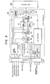
- Fig. 1 shows the general constitution of a first embodiment of the present invention including a magnetic disk apparatus.
- the magnetic disk drive system comprises a magnetic disk apparatus 1, a disk controller 100 and a host computer 20. Enclosed by alternate long and short dash lines is the magnetic disk apparatus 1 is provided with a plurality of data disks 2 and a read/write head 3 for reading data from and writing data in the data disks 2. At least one of the data disks 2 has servo areas 4 storing servo information.
- a spindle motor 5 for rotating the data disks 2 is provided with a position detector 6. In the first embodiment, the position detector 6 produces a pulse signal indicating the starting point of rotation of the data disks 2 or the servo data write starting point in writing servo data.
- the position detector 6 produces index signals indicating the respective start positions of servo areas 4, respectively.
- the output signal of the position detector 6 is given to a user index generator 7 enclosed by broken lines, which is one of the essential component of the magnetic disk drive system of the present invention.
- the user index producing circuit 7 has an index detect circuit 8 which produces a signal A indicating a position immediately before the servo area 4.
- the signal A is applied to a delay circuit 9, and then the delay circuit 9 produces a signal B indicating a position immediately behind the servo area 4.
- the two signals A and B are applied to a switching circuit 10.
- a switching control circuit 11 controls the switching circuit 10 to give either the signal A or the signal B as a user index signal 41 through an interface circuit 17 to the disk controller 100.
- a write gate signal 42 to be transmitted through the interface circuit 17 to a read/write amplifier 12 is given to the switching control circuit 11.
- the signals A and B are given to the switching control circuit 11 in addition to the write gate signal 42.
- the switching control circuit 11 detects the start of format write process of the disk controller 11 from the write gate signal 42 and the signal B. In a format write mode, the switching control circuit 11 controls the switching circuit 10 so that the signals A and B are given through the interface circuit 17 to the disk controller 100 while, in modes other than the format write mode, the switching control circuit 11 controls the switching circuit 10 so that the signal B is given as a user index signal 41 through the interface circuit 17 to the disk controller 100.
- the signal B indicating a position behind the servo area is transmitted as a user index signal from the magnetic disk apparatus 1 to the disk controller 100 in modes other than the format write mode, such as a data write mode and a data read mode, while the signal A indicating a position before the servo area is given as a user index signal 41 in addition to the signal B to the disk controller 100 in the format write mode.
- a waveform shaping circuit 13 for shaping the waveforms of data signals provided by the read/write amplifier 12, an actuator 14 for actuating the read/write head 3, an actuator drive circuit 15 for driving an actuator 14, and a microprocessor 16 serving as a servo controller, which are substantially the same in circuit constitution as the corresponding conventional circuit elements.
- the switching control circuit 11 comprises an edge trigger delay circuit 18 which produces a pulse of a fixed pulse width upon the reception of the signal B at a point corresponding to the leading edge of the signal B, an edge trigger delay circuit 19 which produces a pulse of a fixed width upon the reception of the signal A at a point corresponding to the trailing edge of the signal A, and a flip-flop circuit 20.
- the edge trigger delay circuit 18 Upon the reception of the signal B, the edge trigger delay circuit 18 produces a pulse of a fixed pulse width to convert the condition of the flip-flop circuit 20 at the trailing edge of the pulse so that the flip-flop circuit 20 samples and stores a write gate signal 42 provided by the disk controller 100.
- the write gate signal 42 is to become active (low) before the trailing edge of the pulse provided by the edge trigger delay circuit 18.
- the flip-flop circuit 20 becomes a state corresponding to the high write gate signal 42 and provide an high Q output.
- the switching circuit 10 selects the signal A as the user index signal 41 and, when a low Q output, selects the signal B as the user index signal 41. Accordingly, in the format write mode, the switching circuit 10 gives the signal A as the user index signal 41 in addition to the signal B to the disk controller 100.
- the edge trigger delay circuit 19 upon the reception of the signal A, the edge trigger delay circuit 19 produces a pulse of a fixed pulse width at a point corresponding to the trailing edge of the signal A.
- the pulses produced by the edge trigger delay circuit 19 is applied to the reset input terminal R of the flip-flop circuit 20 to reset the flip-flop circuit 20.
- the flip-flop circuit 20 provides a Q output signal to change the switching condition of the switching circuit 10 from a condition for selecting the signal A to a condition for selecting the signal B.
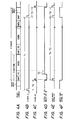
- Figs. 3A to 3H are waveforms of signals provided by the essential components of the first embodiment in the format write mode.
- Fig 3A typically shows a track pattern on the data disk 2; Figs. 3B and 3C show the respective waveforms of the signals A and B, respectively; Figs. 3D and 3E show the respective waveforms of the output signals of the edge trigger delay circuits 18 and 19, respectively; Fig. 3F shows the waveform of the output Q of the flip-flop circuit 20; Fig. 3G shows the waveform of the user index signal 41; Fig. 3H shows the waveform of the write gate signal 42 produced by the disk controller 100 on the basis of the user index signal 41.
- the switching circuit 10 selects the signal B when the output Q of low-level is provided, and selects the signal A when the output Q of high-level is provided.
- each servo area 4 on the data disk 2 lies between the signal A and the signal B in respect of time, while the period of the format write process extends from the signal B to the signal A as apparent from the write gate signal 42, in which nothing is written in the servo area 4 of the data disk 2, so that the servo data is protected.
- Figs. 4A to 4F show the essential portions of the waveforms shown in Figs. 3A to 3H relating to the format write mode start section.
- each track has a plurality of sectors, for example, thirty-two sectors or sixty-four sectors, each comprising a gap area GAP, an ID area ID and a data area DATA.
- the output signal of the edge trigger delay circuit 18 starts rising immediately before, namely, a time interval T 3 before, the data area of the first sector of each track. Therefore, it is possible to discriminate the write process of the disk controller 100 among a format write process and a data write process, because the write gate signal 42 is high, the Q output of the flip-flop circuit 20 is low and the switching circuit 10 is a condition for selecting the signal B at a point corresponding to the leading edge of the output signal of the edge trigger delay circuit 18 in the data write mode.
- Fig. 5 Shown in Fig. 5 showing the general constitution of the disk controller 100 shown in Fig. 1 are a data buffer 101, a sequencer 102, a serial-parallel converter 103, a parallel-serial converter 104, and an I/O processor 105.
- the data buffer 101 stores format information for a plurality of tracks or enables simultaneous data transfer between the magnetic disk apparatus 1 and the disk controller 100 and data transfer between the disk controller 100 and the host computer 200. Therefore, format information for the next track has been stored in the data buffer 101 before the end of a format write process for writing format information in the preceding track.
- the disk controller 100 is able to execute formatting process for formating a track on another data surface immediately after ending formatting the track on the preceding data surface.
- a magnetic disk drive system, in a second embodiment, according to the present invention will be described hereinafter with reference to Figs. 6 to 11.
- Fig. 6, similarly to Fig. 1, shows the constitution of a magnetic disk apparatus including an interface circuit 17.
- the magnetic disk apparatus shown in Fig. 6 and that shown in Fig. 1 are the same in constitution.
- parts similar or corresponding to those described with reference to Fig. 1 are denoted by the same reference numerals.
- a motor driver 21, an offset detector 22 and a head selector circuit 23, which are not shown in Fig. 1, are shown in Fig. 6 .
- the second embodiment employs a user index generator 24 which is different from that of the first embodiment.
- the offset detector 22 comprises an amplifier and an AD converter.
- the offset detector 22 is the same in constitution as the conventional offset detector.
- the offset detector 22 gives an offset value for servo to a microprocessor 16.
- the second embodiment employs ST506 (Shugart) as an interface circuit 17.
- ST506 Silicone
- the head selector circuit 23 selects the uppermost head 3 compulsorily to read servo data from the servo area 4 regardless of the selection of any other head 3 among the rest of the heads 3.
- the head selector circuit 23 is controlled by a signal given thereto from the microprocessor 16.
- Such a circuit constitution is the same as that of the corresponding conventional circuit.
- the user index generator 24 employed in the second embodiment is different from the user index generator 7 employed in the first embodiment.
- a magnet buried in a rotary member of a spindle motor 5 in the second embodiment is different in width from that employed in the first embodiment, and the time when a position detector 6 provides an output signal coincides with the time when the servo area 4 passes below the head 3. Accordingly, upon the passage of the magnet by the position detector 6, the level of the index signal changes from high to low.
- the user index generator 24 Upon the detection of the leading edge of the index signal, the user index generator 24 provides a user index signal 41.
- the user index generator 24 provides the user index signal 41 also when the leading edge of the index signal is detected and a write gate signal 42 is low at the moment when thetrailing edge of the index signal is detected. While the write gate signal is low, the head 3 is able to write in the data surface.
- the write gate signal 42 is low at a moment corresponding to the trailing edge of the index signal only in the format write mode.
- Fig. 7A shows an embodiment of the user index generator 24 and Figs. 8A to 8H are the respective waveforms of signals produced by the essential components of the user index generator 24. Shown in Fig. 7A are flip-flop circuits 25, 26 and 27, and a delay circuit 28. The flip-flop circuit 26 produces a negative pulse at the output terminal Q at a moment corresponding to the leading edge of the index signal provided by the position detector 6. An RC circuit connected across the Q output terminal and the clear terminal CLR of the flip-flop circuit 26 determines the pulse width of the negative pulse.
- Figs. 8A and 8B show the respective waveforms of the index signal and the output signal at the Q output terminal, respectively.
- the delay circuit 28 delays the Q output signal by a fixed time to provide a negative pulse shown in Fig. 8C.
- a write gate signal shown in Fig. 8D is applied to the terminal D of the flip-flop circuit 27.
- the flip-flop circuit 27 provides an output signal corresponding to the level of the write gate signal 42 through the Q output terminal thereof.
- the write gate signal 42 since the write gate signal 42 corresponding to the format write mode is produced by a disk controller 100, the write gate signal 42 is low in the gap area, in which the delay circuit 28 produces the negative pulse, following the servo area 4, and the flip-flop circuit 27 provides a negative pulse as shown in Fig. 8E through the Q output terminal.
- the microprocessor 16 for servo receives the index signal and the output signal of the flip-flop circuit 27 provided through the output terminal Q, and then, after a predetermined time, produces a signal 29 shown in Fig. 8F.
- the signal 29 is used for providing the user index signal even at a moment corresponding to the trailing edge of the index signal in the format write mode. That is, the signal 29 is applied to the terminal D of the flip-flop, circuit 25. After the level of the signal 29 has changed from high-level to low-level, the signal 29 is used for providing a negative pulse shown in Fig. 8G through the Q output terminal of the flip-flop circuit 25. Consequently, the same user index signal 41 shown in Fig. 8H as that of the first embodiment is produced.
- the microprocessor 16 changes the level of the signal 29 from high to low by changing the level of the signal applied to the terminal D of the flip-flop circuit 26. Accordingly, the flip-flop circuit 25 generates a negative pulse every reception of the index signal at a moment corresponding to the trailing edge of the index signal. On the other hand, since the terminal D of the flip-flop circuit 26 is always low, the flip-flop circuit 26 does not generate any negative pulse at a moment corresponding to the leading edge of the index signal. In such a case, the disk controller 100 uses the user index signal 41 for writing servo data.
- Fig. 7B similarly to Fig. 7A, illustrates another embodiment of the user index generator 24.
- blocks similar to or corresponding to those previously described with reference to Fig. 7A are denoted by the same reference numerals.
- the user index generator 24 shown in Fig. 7B also provides a user index signal 41 only at a moment corresponding to the leading edge of an index signal in the ordinary write mode. In the format write mode the user index generator 24 provides the user index signal 41 also at a moment corresponding to the trailing edge of the index signal.
- a write gate signal 42 is low after the first user index signal 41 has been provided. Accordingly, the input terminal D of a flip-flop circuit 25 is low at a moment corresponding to the trailing edge of the index signal and hence the flip-flop circuit 25 generates a negative pulse at that moment.
- the pulse width of the negative pulse is dependent on the characteristics of a RC circuit connected across the Q output terminal and preset terminal of the flip-flop circuit 25.
- the negative pulse is given as the user index signal 41 through a NOR circuit to the disk controller 100.
- a signal ' applied to the input terminal D of a flip-flop circuit 26 at a moment corresponding to the leading edge of the index signal is inverted and provides an inverted signal, namely, a negative pulse, through the output terminal Q.
- the negative pulse is given as the user index signal 41 through the NOR circuit to the disk controller 100.
- the output of the flip-flop circuit 25, similarly to-that in the foregoing embodiment, does not change at a moment corresponding to the trailing edge of the index signal even when the index signal is applied to the flip-flop circuit 25.
- the magnetic disk apparatus shown in Fig. 6, similarly to that of the first embodiment, is connected through the interface circuit 17 thereof to the disk controller.
- Fig. 9 illustrates a concrete form of the disk controller employed in the second embodiment.
- indicated at 110 is a driver/receiver incorporated into the disk controller.
- the driver/receiver 110 exchanges many signals with the interface circuit 17, however, only signals relating to the present invention are shown in Fig. 9.
- the user index signal 41 is transmitted through the driver/receiver 110 to a timing control circuit 111.
- the timing control circuit 111 comprises, for example, a program logic array (PLA) or a plurality of counters.
- the timing control circuit 111 is substantially the same as the sequencer 102 of the first embodiment in function.
- the timing control circuit 111 receives the user index signal and generates a write gate signal.
- PDA program logic array
- a S/P converter 112 serial-parallel converter
- a P/S converter 113 parallel-serial converter
- a R/W switching circuit 114 read/write switching circuit
- a buffer switching circuit 115 which are controlled by control signals given thereto from the timing control circuit 111 so as to switch read/write and two buffers comprising a first data buffer 117 and a second data buffer 118, respectively
- an I/O processor 116 comprising a microcomputer and memories
- a buffer selector circuit 119 which is controlled by control signals given thereto from the timing control circuit 111
- a command register 120 which stores commands given thereto from a host computer 200
- an interface circuit 121 interconnecting the host computer 200 and the disk controller.
- the disk controller is the same as the conventional disk controller in constitution.
- a format write command given by the host computer 200 is registered in the command register 120, and then the timing control circuit 111 operates in accordance with the format write command.
- the timing control circuit 111 changes the level of the write gate signal 42 to low and starts format writing operation and, upon the reception of the next user index signal 41, the timing control circuit 111 changes the level of the write gate signal 42 to high to complete format writing operation for one track.
- one track in the data surface is formatted.
- format data supplied from the two buffers through the P/S converter 113 is written in the track, in which the servo data written in the servo area 4 is protected and hence the servo data will, as a rule, be never destructed.
- Figs. 10A and 10B are timing charts illustrating the mode of such verification and Fig. 11 is a flow chart showing the manner of the verification.
- Fig. 10A shows the user index signal 41 which is transferred from the magnetic disk apparatus to the disk controller
- Fig. 10B shows the write gate signal 42 which is generated by the timing control circuit 111 according to each mode on the basis of the user index signal 41.
- the level of the write gate signal 42 is changed to low by the first user index signal 41, and then the level of the write gate signal 42 is changed to high by the successive user index signal 41.
- the level of the write gate signal 42 is not changed.
- the host computer 200 gives format information (ID information) for one track to the buffer 117, and then gives a format command to the command register 120.
- the timing control circuit 111 executes format write operation in accordance with the format command.
- a decision is made as to whether or not the user index signal 41 is active (a negative pulse).
- track formating process namely, writing the format information stored in the buffer 117 in the track, is started and the track formating process is continued until the next user index signal 41 provides a negative pulse.
- the track formating mode is ended when the user index signal 41 becomes active again.
- the host computer 200 gives a verify command to the command register 120.
- the timing control circuit 111 make a decision in response to the verify command as to whether or not the user index signal 41 is active.
- the timing control circuit 111 reads the format information stored in the data buffer 117 and the format information written in the data surface to check the exactness of the latter by comparison with the former.
- the timing control circuit 111 checks whether or not the collation of all the bytes of a designated number set as a command parameter have been completed and, when the collation is completed, executes verification ending process.
- the timing control circuit 111 gives a head selection signal designating a head to the magnetic disk apparatus, and then the format write mode and the verify mode are repeated for the next track using the data stored in the data buffer 118.
- the timing control circuit 111 writes optional data at a predetermined position on the track with reference to a specific synchronous data (SYNC) through the format write mode without referring to user index signal 41, which is not directly related to the present invention and hence the detailed description thereof will be omitted.
- SYNC synchronous data
- the servo data may be recorded on any data surface or on a plurality of data surfaces. Generally, when the servo data is recorded on a plurality of data surfaces, the servo data recorded on the data surface nearest to the accessed data surface is read.
- the disk controller uses the user index signal provided by the magnetic disk apparatus as both a format write start signal and a format write end signal. Accordingly, the disk controller receives the user index signal at the end of the servo area 4, which corresponds to the signal B, as the format write start signal, and receives the additional user index signal at the start of the servo area 4, which corresponds to the signal A, as the track end signal. Therefore, the write gate is closed immediately before the servo data and hence the servo data is never destructed.
- a third embodiment of the present invention is capable of detecting the malfunction of the disk controller 100 for the further perfect protection of the servo data.
- Fig. 12 illustrates the third embodiment of the present invention, in which the same parts as those previously described with reference to Fig. 1 are denoted by the same reference numerals.
- the third embodiment comprises a write abnormal detect circuit (WADC) 30 in addition to the arrangement of the first embodiment.
- WADC write abnormal detect circuit
- the WADC 30 incorporated into a magnetic disk apparatus 1' detects the malfunction of the disk controller 100, then invalidate the write gate signal 42 provided by the disk controller 100 for that moment to protect the servo data, and then inform the disk controller 100 of the abnormal write operation.
- Indicated at 31 is a conventional write fault detect circuit which is not included in the first embodiment.
- the write fault detect circuit 31 is included in the interface circuit 17.
- the write fault detect circuit 31 detects three faults, namely, power failure in the magnetic disk apparatus, head malfunction and execution of write operation during seek.
- the write fault detect circuit 31 is unable to detect overwrite attributable to the malfunction of the disk controller.
- a user index generating circuit 7' similarly to that of the first embodiment, generates a signal A and a signal B according to the mode of operation as the user index signal 41.
- the user index generating circuit 7' further generates a signal C after the signal A and before the signal B, which can be easily achieved by means of a delay circuit 9' included in the user index signal generating circuit 7'. That is, the delay circuit 9' produces the signal C from the signal A at a moment after the starting point of the servo area 4 and before the starting point of the servo data included in the servo area 4, in addition to the signal B.
- Fig. 13 illustrates a configuration, by way of example, of the WADC 30.
- the WADC 30 comprises a flip-flop circuit 32 and an inverter 33.
- the WADC 30 receives the signal B and the signal C from the delay circuit 9' and samples the write gate signal 42 provided by a disk controller 100 at the leading edge of the signal C.
- the continuous write operation of the disk controller 100 until the signal C becomes active is regarded as write abnormal, and then the flip-flop circuit 32 provides a Q output to cut off the write gate signal 42 of the disk controller forcibly for servo data protection.
- the write gate signal 42 to be transferred to a read/write amplifier 12, and the Q output are applied to an AND circuit with an inversion output, and then the output of the AND circuit is applied to the R/W control terminal of the read/write amplifier 12. Further, the Q output is sent as a write fault signal together with the output of the conventional write fault detect circuit 31 through the disk controller 100 to a host computer 200.
- Fig. 14A is a schematic illustration of a track format
- Figs. 14B, 14C and 14D show the respective waveforms of the signals A, B and C, respectively
- Fig. 14E shows the waveform of the user index signal given to the disk controller 100
- Fig. 14F shows the waveform of the write gate signal
- Figs. 14A is a schematic illustration of a track format
- Figs. 14B, 14C and 14D show the respective waveforms of the signals A, B and C, respectively
- Fig. 14E shows the waveform of the user index signal given to the disk controller 100
- Fig. 14F shows the waveform of the write gate signal
- FIGS. 14G and 14H show the respective waveforms of the Q output of the WADC 30 and a R/W control signal for controlling the read/write amplifier 12, respectively.
- write abnormal has occurred in the right-hand servo area
- the Q output of the WADC has changed to low
- the R/W control signal has changed to high.
- the read/write amplifier 12 is set by the R/W control signal so as to inhibit write operation before the servo data is destructed even if the write gate signal 42 of the disk controller 100 becomes active (low) during a period corresponding to the servo area.
- the components of the third embodiment functions in the same manner also in a case in which the faulty setting of the disk controller 100 for the number of bytes of write data, which also is possible to destruct the servo data.
- Fig. 16 shows the respective modifications of the user index generating circuit and the WADC of the third embodiment.
- indicated at 24' is a user index generating circuit and at 30' is a WADC (write abnormal detect circuit).
- the signal produced by-a position detector 6 becomes low in an area corresponding to the servo area in the this modification like that in the second embodiment (Fig. 6).
- This signal is applied through a RC filter and a Schmitt trigger inverter to the clock terminal CK of a flip-flop circuit 38, and through another Schmitt'trigger inverter to a positive edge trigger circuit 37.
- positive edge trigger circuit 37 produces a negative pulse. This pulse is applied to the reset terminal (R) of the flip-flop circuit 38.
- the write gate signal 42 is applied to the data input terminal (D) of the flip-flop circuit 38.
- the flip-flop circuit 38 is triggered by the trailing edge of the index signal to latch the write gate signal 42 and produces a user index signal at the output terminal Q.
- the inverted output terminal Q of the flip-flop circuit 38 is connected through a delay circuit 39 and a Schmitt trigger inverter to the set terminal S.
- the write gate signal 42 latched by the flip-flop circuit 38 using the trailing-edge of the index signal as a trigger is set by the leading edge of the inverted output (Q output).
- the flip-flop circuit is set after a predetermined time.
- the user index signal 41 is always provided at a moment corresponding to the leading edge of the index signal, and the user index signal is provided at a moment corresponding to the trailing edge of the index signal only when the level of the write gate signal 42 is low.
- the WADC 30' comprises, as principal components, a flip-flop circuit 47 which receives the write gate signal 42 at the data input terminal D through a Schmitt trigger inverter, and a delay circuit 46.
- the index signal is delayed by a predetermined time by the delay circuit 46. That is, the trailing edge of the index signal is delayed by a predetermined time to latch the write gate signal 42 a moment after the start of the servo area 4, and then the write gate signal 42 is provided at the output terminal Q of the flip-flop circuit 46.
- the write gate signal 42 is provided as a write abnormal signal.
- the rest of the constitution and functions are the same as those of the third embodiment shown in Fig. 12.
- a fourth embodiment of the present invention will. be described hereinafter with reference to Figs. 17 to 20, in which the same parts as those previously described with reference to Fig. 12 are denoted by the same reference numerals.
- a magnetic disk apparatus employed in the fourth embodiment also is provided with a write abnormal detect circuit.
- Fig. 17, indicated at 34 is a write abnormal detect circuit.
- An output a of the write abnormal detect circuit 34 is sent as a write fault signal 45 together with a signal provided by a write fault detect circuit 31 to a disk controller 100.
- An output b of the write abnormal detect circuit 34 is given to a microprocessor 16 to inform the microprocessor 16 of the abnormal operation of the disk controller 100 and to register the position of write abnormal.
- the destructed servo data is not used thereafter and servo data of the adjacent track is used in place of the destructed servo data.
- the microcomputer 16 stores the servo data of the adjacent track in a memory incorporated therein.
- the write abnormal detect circuit 34 similarly to the write abnormal detect circuit 30 shown in Fig. 13, generates the output a by means of a flip-flop circuit 32 and an inverter 33, and the output b by means of a flip-flop circuit 35 and an inverter 36.
- a signal produced by inverting the write gate signal 42 produced by a disk controller 100 by the inverter 33 is applied to the data input terminal D of the flip-flop circuit 32, while a signal produced by inverting the signal C by the inverter 36 is applied to the clock input terminal CK of the flip-flop circuit 32.
- the trailing edge of the signal C corresponds to the start of servo data.
- the signal B is applied to the reset terminal R of the flip-flop circuit 35.
- Figs. 19A to 19H similarly to Figs. 14A to 14H, the timing of operation of the write abnormal detect circuit 34.
- a track format and waveforms shown in Figs. 19A to 19F are the same as those shown in Figs. 14A to 14H, respectively.
- Figs. 19G and 19H show the waveforms of the outputs a and b of the write abnormal detect circuit 34.
- a signal produced by inverting the signal C is applied to the clock input terminal of the flip-flop circuit 35, however, a timing signal indicating the start of another servo data may be applied to the clock input terminal of the flip-flop circuit 35 for the same effect.
- the fourth embodiment has been described with reference to a case in which write abnormal occurred in the format write mode, naturally, the fourth embodiment is able to deal with a case in which write abnormal occurs in the data write mode.
- Fig. 20 is a flow chart showing the general procedure of opera- a tion of a magnetic disk apparatus 1" employed in the fourth embodiment, which is different from the manner of operation of the magnetic disk apparatus of the foregoing embodiment.
- the position of destructed servo data can be registered in a microprocessor 16 without modifying a R/W control signal for controlling a read/write amplifier 12.
- the third and fourth embodiments have been described as each having a write abnormal detect circuit in addition to the components of the first embodiment, naturally, the circuit of the second embodiment shown in Fig. 6 may be provided additionally with a write abnormal detect circuit. In such a case, since a write fault detect circuit 31 is included in the ST506 employed as an interface circuit 17, the circuit needs some modification, which is obvious to those skilled in the art and hence the description thereof will be omitted.
- the disk controller executes a faulty control operation causing write abnormal in the servo data area due to setting the disk controller for faulty software or the like
- write abnormal is detected and the disk controller and the host computer are informed of write abnormal, so that measures are taken to deal with write abnormal, which improves the reliability of the system remarkably.
- impediment in the following servocontrol can be prevented by forcibly interrupting write abnormal in the magnetic disk apparatus to protect the servo data or by registering the position of the destructed servo data in the servo microcomputer.
- the process time of the format write mode can be remarkably reduced without adding additional circuit elements to the circuit of the disk controller by selectively using the user index signals given from the disk apparatus to the disk controller according to the operating mode of the disk apparatus. Furthermore, since the disk apparatus is able to discriminate independently the mode of operation designated by the host computer by means of the write gate signal, the disk apparatus is able to cope independently with write abnormal to protect the servo data without delay, even when write abnormal is caused by the abnormal operation of the disk controller.
Abstract
Description
- The present invention relates to a disk apparatus of a data surface servo system for use in a disk drive system.
- Disk drive systems of various servo systems, such as a magnetic disk drive system comprising a magnetic disk apparatus, a host computer, and a disk controller interconnecting the magnetic disk apparatus and the host computer, have been provided. A disk drive system of a data surface servo system is one of those known disk drive systems. According to such a data side servo system, servo data is written in a servo area of a disk for entering data at least once every round. The servo data is used for producing control signals for controlling a positioning servomechanism for aligning a magnetic head with the center of the track.
- In a data surface servo system disclosed, for example, in U.S. Pat. No. 4,396,959, a detector provided on a spindle motor for rotatively driving a disk produces an index signal immediately before the servo area. Then, the index signal is applied to the servo controller of the magnetic disk apparatus to produce a write inhibit signal for masking a write gate signal given by a disk controller to the magnetic disk apparatus during write operation to protect servo data previously recorded on the data side of the disk. After being delayed by the servo controller, the index signal is given to the disk controller for producing a write gate signal. Consequently, since the format write operation of the disk controller continues from a moment when the leading edge of the delayed index signal is detected to a moment when the leading edge of the next delayed index signal, the operation of the disk controller is held unavoidably from the end of writing the format on one track to the start of writing the next format for a latency period corresponding to one round.
- To eliminate such inconvenience, a write gate signal may be produced by giving index signals produced immediately before and immediately after the servo area, respectively, in the magnetic disk apparatus to the disk controller. However, the current disk controller is incapable of discriminating whether the index signals are those produced immediately before or immediately after the servo area. Accordingly, the current disk controller is unable to be used for producing the write gate signal in such a manner. To provide the current disk controller with an index signal discriminating function, additional circuits in terms of gates on the order of approximately 600 gates need to be incorporated into the disk controller, which is a considerable increase in the circuits.
- Thus, a latency period corresponding to one round is indispensable to the known disk drive system disclosed in U.S. Pat. No. 4,396,959 for a format data verify process or for a format write process for the next track, after the end of a format write process for the preceding track in the format mode, and hence the disk drive system requires much time for the format process. Even if the disk apparatus is constituted so as to give always two index signals immediately before and immediately after the servo area to the disk controller, the current disk controller is unable to function without requiring considerable increase in circuit.
- It is therefore a general object of the present invention to provide a disk drive system capable of reducing time for format write process without requiring considerable modification of a disk controller.
- Another object of the present invention is to provide a disk apparatus capable of independently establishing operation mode on the basis of a control signal given thereto from a disk controller.
- A further object of the present invention is to provide a magnetic disk drive system employing an existing disk controller and capable of greatly reducing format write process time.
- Still a further object of the present invention is to provide a magnetic disk apparatus capable of independently establishing operation mode such as format write mode on the basis of a write control signal given thereto from a disk controller.
- To achieve the objects of the invention, a disk drive system according to the present invention has a disk apparatus capable of selecting a user index signal to be given to a disk controller in accordance with the operation mode of the system. That is, in a format write mode, the disk apparatus gives signals respectively indicating the start and end of a servo area timely to the disk controller and, in a . mode other than the format write mode, gives a signal indicating the end of a servo area timely to the disk controller.
- The disk apparatus has an operation mode detecting means capable of independently detecting the operation mode of the system on the basis of a control signal given,thereto from the disk controller and, upon the detection of the format write mode by the operation mode detecting means, the disk apparatus gives user index signals, namely, signals respectively indicating the start and end of the servo area to the disk controller., When the detected operation mode is not the format write mode, the disk apparatus gives a signal indicating the end of the servo area as a user index signal to the disk controller.
- The operation mode detecting means receives a write gate signal, i.e., a data write control signal from the disk controller, and a servo area end signal
, and then discriminates the operation mode among a format write mode and other modes by discriminating the level of the write control signal a predetermined time after receiving the servo area end signal indicating the end of the servo area. - Thus, in the format write mode, the disk controller is able to receive a format write start signal and a format write end signal indicating points of starting and ending format write operation for one track, respectively, as user index signals from the disk apparatus to avoid abnormal writing in the servo area, and is also able to execute format,write process for the next track without a latency period, so that the latency period is reduced greatly. In a mode other than the format write mode, the disk controller receives only the servo area end signal indicating the end of the servo area as a user index signal from the disk apparatus, and hence the disk controller is able to execute operation modes other than the format write mode without requiring the considerable modification of the circuit thereof.
- Furthermore, according to the present invention, the disk apparatus is provided additionally, to detect abnormal writing in the servo area, with a write abnormal detecting means for detecting the level of the write control signal provided by the disk controller a predetermined time after the servo area start signal indicating the start of the servo area has been provided. The disk apparatus is provided further with a means for forcibly invalidating the write control signal upon the detection of the write abnormal by the detecting means. Similarly, the disk apparatus is provided with a means for giving a write fault signal to the disk controller upon the detection of write abnormal by the write abnormal detecting means.
- Still further, the disk apparatus is provided with a signal generating means for generating a servo area start signal and a servo area end signal on the basis of the output signal of a phase detecting means for detecting the angular phase of the disk.
- The present invention will be described hereinafter as applied to a magnetic disk apparatus by way of example, however, the present invention is not limited thereto in application, but the present invention is applicable also to other disk apparatus including an optical disk apparatus.
-
- Figure 1 is a block diagram showing the constitution of a magnetic disk drive system including a magnetic disk apparatus, in a first embodiment, according to the present invention;
- Figure 2 is a block diagram showing the concrete circuit constitution of a
switching control circuit 11 employed in the magnetic disk drive system of Fig. 1; - Figures 3A to 3H are waveform charts showing the respective waveforms of signals produced by the essential components of the magnetic disk drive system of Fig. 1;
- Figures 4A to 4F are partially enlarged waveform charts showing the respective essential portions of some of the signals among the signals shown in Figs. 3A to 3H;
- Figure 5 is a block diagram showing the concrete circuit constitution of a
disk controller 100 employed in the magnetic disk drive system of Fig. 1; - Figure 6 is a block diagram showing the constitution of a magnetic disk drive system, in a second embodiment, according to the present invention;
- Figures 7A and 7B are block diagrams showing the concrete circuit constitution of a user index
signal generating circuit 24 employed in the magnetic disk drive system of Fig. 6; - Figures 8A to 8H are waveform charts showing the respective waveforms of signals produced by the essential components of the magnetic disk drive system of Fig. 6;
- Figure 9 is a block diagram showing the concrete circuit constitution of a disk controller employed in the magnetic disk drive system of Fig. 6;
- Figures 10A and 10B are diagrams showing the operation mode and the waveforms of signals produced by the essential components of the magnetic disk drive system of Fig. 6;
- Figure 11 is a flow chart showing the general operation of the magnetic disk drive system of Fig. 6;
- Figure 12 is a block diagram showing the circuit constitution of a magnetic disk drive system including a magnetic disk apparatus employed, in a third embodiment, according to the present invention;
- Figure 13 is a block diagram showing the concrete constitution of a write abnormal detect circuit employed in the magnetic disk drive system of Fig. 12;
- Figures 14A to 14H are waveform charts showing the respective waveforms of signals produced by the essential components of the magnetic disk drive system of Fig. 12;
- Figure 15 is a flow chart showing the general operation of the magnetic disk drive system of Fig. 12;
- Figure 16 is a block diagram showing the respective concrete circuit constitutions of the modifications of the user index signal producing circuit and the write abnormal detect circuit of the magnetic disk drive system of Fig. 12;
- Figure 17 is a block diagram showing the general constitution of a magnetic disk drive system including a magnetic disk apparatus, in a fourth embodiment, according to the present invention;
- Figure 18 is a block diagram showing the concrete circuit constitution of a write abnormal detect circuit employed in the magnetic disk drive system of Fig. 17;
- Figures 19A to 19H are waveform charts showing the respective waveforms of signals produced by the essential components of the magnetic disk drive system of Fig. 17; and
- Figure 20 is a flow chart showing the general operation process of the magnetic disk drive system of Fig. 17.
- Preferred embodiments of the present invention will be described hereinafter with reference to the accompanying drawings.
- Fig. 1 shows the general constitution of a first embodiment of the present invention including a magnetic disk apparatus. The magnetic disk drive system comprises a
magnetic disk apparatus 1, adisk controller 100 and ahost computer 20. Enclosed by alternate long and short dash lines is themagnetic disk apparatus 1 is provided with a plurality ofdata disks 2 and a read/writehead 3 for reading data from and writing data in thedata disks 2. At least one of thedata disks 2 hasservo areas 4 storing servo information. Aspindle motor 5 for rotating thedata disks 2 is provided with aposition detector 6. In the first embodiment, theposition detector 6 produces a pulse signal indicating the starting point of rotation of thedata disks 2 or the servo data write starting point in writing servo data. That is, theposition detector 6 produces index signals indicating the respective start positions ofservo areas 4, respectively. The output signal of theposition detector 6 is given to auser index generator 7 enclosed by broken lines, which is one of the essential component of the magnetic disk drive system of the present invention. The userindex producing circuit 7 has an index detectcircuit 8 which produces a signal A indicating a position immediately before theservo area 4. The signal A is applied to adelay circuit 9, and then thedelay circuit 9 produces a signal B indicating a position immediately behind theservo area 4. The two signals A and B are applied to aswitching circuit 10. A switchingcontrol circuit 11 controls the switchingcircuit 10 to give either the signal A or the signal B as auser index signal 41 through aninterface circuit 17 to thedisk controller 100. - A
write gate signal 42 to be transmitted through theinterface circuit 17 to a read/write amplifier 12 is given to the switchingcontrol circuit 11. The signals A and B are given to the switchingcontrol circuit 11 in addition to thewrite gate signal 42. The switchingcontrol circuit 11 detects the start of format write process of thedisk controller 11 from thewrite gate signal 42 and the signal B. In a format write mode, the switchingcontrol circuit 11 controls the switchingcircuit 10 so that the signals A and B are given through theinterface circuit 17 to thedisk controller 100 while, in modes other than the format write mode, the switchingcontrol circuit 11 controls the switchingcircuit 10 so that the signal B is given as auser index signal 41 through theinterface circuit 17 to thedisk controller 100. In the first embodiment, the signal B indicating a position behind the servo area is transmitted as a user index signal from themagnetic disk apparatus 1 to thedisk controller 100 in modes other than the format write mode, such as a data write mode and a data read mode, while the signal A indicating a position before the servo area is given as auser index signal 41 in addition to the signal B to thedisk controller 100 in the format write mode. - Also shown in Fig. 1 are a
waveform shaping circuit 13 for shaping the waveforms of data signals provided by the read/write amplifier 12, anactuator 14 for actuating the read/write head 3, anactuator drive circuit 15 for driving anactuator 14, and amicroprocessor 16 serving as a servo controller, which are substantially the same in circuit constitution as the corresponding conventional circuit elements. - The manner of operation of the first embodiment shown in Fig. 1 will be described hereinafter with reference to Figs. 2 and 3A to 3H.
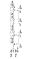
- Referring to Fig. 2, the switching
control circuit 11 comprises an edgetrigger delay circuit 18 which produces a pulse of a fixed pulse width upon the reception of the signal B at a point corresponding to the leading edge of the signal B, an edgetrigger delay circuit 19 which produces a pulse of a fixed width upon the reception of the signal A at a point corresponding to the trailing edge of the signal A, and a flip-flop circuit 20. Upon the reception of the signal B, the edgetrigger delay circuit 18 produces a pulse of a fixed pulse width to convert the condition of the flip-flop circuit 20 at the trailing edge of the pulse so that the flip-flop circuit 20 samples and stores awrite gate signal 42 provided by thedisk controller 100. When thedisk controller 100 is in the format write mode, thewrite gate signal 42 is to become active (low) before the trailing edge of the pulse provided by the edgetrigger delay circuit 18. The flip-flop circuit 20 becomes a state corresponding to the highwrite gate signal 42 and provide an high Q output. When the flip-flop circuit 20 provides the high Q output, the switchingcircuit 10 selects the signal A as theuser index signal 41 and, when a low Q output, selects the signal B as theuser index signal 41. Accordingly, in the format write mode, the switchingcircuit 10 gives the signal A as theuser index signal 41 in addition to the signal B to thedisk controller 100. - On the other hand, upon the reception of the signal A, the edge
trigger delay circuit 19 produces a pulse of a fixed pulse width at a point corresponding to the trailing edge of the signal A. The pulses produced by the edgetrigger delay circuit 19 is applied to the reset input terminal R of the flip-flop circuit 20 to reset the flip-flop circuit 20. Then, the flip-flop circuit 20 provides a Q output signal to change the switching condition of the switchingcircuit 10 from a condition for selecting the signal A to a condition for selecting the signal B. - Figs. 3A to 3H are waveforms of signals provided by the essential components of the first embodiment in the format write mode.
- Fig 3A typically shows a track pattern on the
data disk 2; Figs. 3B and 3C show the respective waveforms of the signals A and B, respectively; Figs. 3D and 3E show the respective waveforms of the output signals of the edgetrigger delay circuits flop circuit 20; Fig. 3G shows the waveform of theuser index signal 41; Fig. 3H shows the waveform of thewrite gate signal 42 produced by thedisk controller 100 on the basis of theuser index signal 41. The switchingcircuit 10 selects the signal B when the output Q of low-level is provided, and selects the signal A when the output Q of high-level is provided. - As is obvious from Figs. 3A to 3H, each
servo area 4 on thedata disk 2 lies between the signal A and the signal B in respect of time, while the period of the format write process extends from the signal B to the signal A as apparent from thewrite gate signal 42, in which nothing is written in theservo area 4 of thedata disk 2, so that the servo data is protected. - Figs. 4A to 4F show the essential portions of the waveforms shown in Figs. 3A to 3H relating to the format write mode start section.
- Referring to Fig. 4A showing the track format of the
data disk 2, each track has a plurality of sectors, for example, thirty-two sectors or sixty-four sectors, each comprising a gap area GAP, an ID area ID and a data area DATA. The output signal of the edgetrigger delay circuit 18 starts rising immediately before, namely, a time interval T3 before, the data area of the first sector of each track. Therefore, it is possible to discriminate the write process of thedisk controller 100 among a format write process and a data write process, because thewrite gate signal 42 is high, the Q output of the flip-flop circuit 20 is low and the switchingcircuit 10 is a condition for selecting the signal B at a point corresponding to the leading edge of the output signal of the edgetrigger delay circuit 18 in the data write mode. - Shown in Fig. 5 showing the general constitution of the
disk controller 100 shown in Fig. 1 are adata buffer 101, asequencer 102, a serial-parallel converter 103, a parallel-serial converter 104, and an I/O processor 105. Thedata buffer 101 stores format information for a plurality of tracks or enables simultaneous data transfer between themagnetic disk apparatus 1 and thedisk controller 100 and data transfer between thedisk controller 100 and thehost computer 200. Therefore, format information for the next track has been stored in thedata buffer 101 before the end of a format write process for writing format information in the preceding track. Accordingly, when the headselect signals 44 of thesequencer 102 is changed in a time interval T2 between the signal A and the signal B to subject another data surface of the same cylinder to formatting process, thedisk controller 100 is able to execute formatting process for formating a track on another data surface immediately after ending formatting the track on the preceding data surface. - A magnetic disk drive system, in a second embodiment, according to the present invention will be described hereinafter with reference to Figs. 6 to 11.
- Fig. 6, similarly to Fig. 1, shows the constitution of a magnetic disk apparatus including an
interface circuit 17. Basically, the magnetic disk apparatus shown in Fig. 6 and that shown in Fig. 1 are the same in constitution. In Fig. 6, parts similar or corresponding to those described with reference to Fig. 1 are denoted by the same reference numerals. In Fig. 6, amotor driver 21, an offsetdetector 22 and ahead selector circuit 23, which are not shown in Fig. 1, are shown in Fig. 6. The second embodiment employs auser index generator 24 which is different from that of the first embodiment. The offsetdetector 22 comprises an amplifier and an AD converter. The offsetdetector 22 is the same in constitution as the conventional offset detector. The offsetdetector 22 gives an offset value for servo to amicroprocessor 16. The second embodiment employs ST506 (Shugart) as aninterface circuit 17. Whenservo areas 4 are formed only on the uppermost data surface among the four data surfaces of twodata disks 2 and fourheads 3 are provided as shown in Fig. 6, thehead selector circuit 23 selects theuppermost head 3 compulsorily to read servo data from theservo area 4 regardless of the selection of anyother head 3 among the rest of theheads 3. Thehead selector circuit 23 is controlled by a signal given thereto from themicroprocessor 16. Such a circuit constitution is the same as that of the corresponding conventional circuit. - The
user index generator 24 employed in the second embodiment is different from theuser index generator 7 employed in the first embodiment. A magnet buried in a rotary member of aspindle motor 5 in the second embodiment is different in width from that employed in the first embodiment, and the time when aposition detector 6 provides an output signal coincides with the time when theservo area 4 passes below thehead 3. Accordingly, upon the passage of the magnet by theposition detector 6, the level of the index signal changes from high to low. Upon the detection of the leading edge of the index signal, theuser index generator 24 provides auser index signal 41. Theuser index generator 24 provides theuser index signal 41 also when the leading edge of the index signal is detected and awrite gate signal 42 is low at the moment when thetrailing edge of the index signal is detected. While the write gate signal is low, thehead 3 is able to write in the data surface. In the second embodiment, in particular, thewrite gate signal 42 is low at a moment corresponding to the trailing edge of the index signal only in the format write mode. - Fig. 7A shows an embodiment of the
user index generator 24 and Figs. 8A to 8H are the respective waveforms of signals produced by the essential components of theuser index generator 24. Shown in Fig. 7A are flip-flop circuits delay circuit 28. The flip-flop circuit 26 produces a negative pulse at the output terminal Q at a moment corresponding to the leading edge of the index signal provided by theposition detector 6. An RC circuit connected across the Q output terminal and the clear terminal CLR of the flip-flop circuit 26 determines the pulse width of the negative pulse. Figs. 8A and 8B show the respective waveforms of the index signal and the output signal at the Q output terminal, respectively. Thedelay circuit 28 delays the Q output signal by a fixed time to provide a negative pulse shown in Fig. 8C. A write gate signal shown in Fig. 8D is applied to the terminal D of the flip-flop circuit 27. When the negative pulse provided by thedelay circuit 28 is applied to the terminal CK of the flip-flop circuit 27, the flip-flop circuit 27 provides an output signal corresponding to the level of thewrite gate signal 42 through the Q output terminal thereof. As illustrated in Fig. 8D, since thewrite gate signal 42 corresponding to the format write mode is produced by adisk controller 100, thewrite gate signal 42 is low in the gap area, in which thedelay circuit 28 produces the negative pulse, following theservo area 4, and the flip-flop circuit 27 provides a negative pulse as shown in Fig. 8E through the Q output terminal. - The
microprocessor 16 for servo receives the index signal and the output signal of the flip-flop circuit 27 provided through the output terminal Q, and then, after a predetermined time, produces asignal 29 shown in Fig. 8F. Thesignal 29 is used for providing the user index signal even at a moment corresponding to the trailing edge of the index signal in the format write mode. That is, thesignal 29 is applied to the terminal D of the flip-flop,circuit 25. After the level of thesignal 29 has changed from high-level to low-level, thesignal 29 is used for providing a negative pulse shown in Fig. 8G through the Q output terminal of the flip-flop circuit 25. Consequently, the sameuser index signal 41 shown in Fig. 8H as that of the first embodiment is produced. - In a mode other than the format write mode, since the write gate signal shown in Fig. 8D has not become low, where writing data on the data surface is possible before a moment when the negative pulse is provided by the
delay circuit 28, the signal given through the Q output terminal of the flip-flop circuit 27 to themicroprocessor 16 is never a negative pulse and hence the themicroprocessor 16 continues providing thehigh signal 29. Accordingly, the flip-flop circuit 25 does not produce any negative pulse, and hence only a negative pulse is given as the user index signal to thedisk controller 100 at a moment corresponding to the leading edge of the index signal. - The
microprocessor 16 changes the level of thesignal 29 from high to low by changing the level of the signal applied to the terminal D of the flip-flop circuit 26. Accordingly, the flip-flop circuit 25 generates a negative pulse every reception of the index signal at a moment corresponding to the trailing edge of the index signal. On the other hand, since the terminal D of the flip-flop circuit 26 is always low, the flip-flop circuit 26 does not generate any negative pulse at a moment corresponding to the leading edge of the index signal. In such a case, thedisk controller 100 uses theuser index signal 41 for writing servo data. - Fig. 7B, similarly to Fig. 7A, illustrates another embodiment of the
user index generator 24. In Fig. 7B, blocks similar to or corresponding to those previously described with reference to Fig. 7A are denoted by the same reference numerals. Theuser index generator 24 shown in Fig. 7B also provides auser index signal 41 only at a moment corresponding to the leading edge of an index signal in the ordinary write mode. In the format write mode theuser index generator 24 provides theuser index signal 41 also at a moment corresponding to the trailing edge of the index signal. - In the format write mode, a
write gate signal 42 is low after the firstuser index signal 41 has been provided. Accordingly, the input terminal D of a flip-flop circuit 25 is low at a moment corresponding to the trailing edge of the index signal and hence the flip-flop circuit 25 generates a negative pulse at that moment. The pulse width of the negative pulse is dependent on the characteristics of a RC circuit connected across the Q output terminal and preset terminal of the flip-flop circuit 25. The negative pulse is given as theuser index signal 41 through a NOR circuit to thedisk controller 100. A signal ' applied to the input terminal D of a flip-flop circuit 26 at a moment corresponding to the leading edge of the index signal is inverted and provides an inverted signal, namely, a negative pulse, through the output terminal Q. The negative pulse is given as theuser index signal 41 through the NOR circuit to thedisk controller 100. - Since the write gate signal is high in the ordinary write mode, the output of the flip-
flop circuit 25, similarly to-that in the foregoing embodiment, does not change at a moment corresponding to the trailing edge of the index signal even when the index signal is applied to the flip-flop circuit 25. - The magnetic disk apparatus shown in Fig. 6, similarly to that of the first embodiment, is connected through the
interface circuit 17 thereof to the disk controller. Fig. 9 illustrates a concrete form of the disk controller employed in the second embodiment. In Fig. 9, indicated at 110 is a driver/receiver incorporated into the disk controller. The driver/receiver 110 exchanges many signals with theinterface circuit 17, however, only signals relating to the present invention are shown in Fig. 9. Theuser index signal 41 is transmitted through the driver/receiver 110 to atiming control circuit 111. Thetiming control circuit 111 comprises, for example, a program logic array (PLA) or a plurality of counters. Thetiming control circuit 111 is substantially the same as thesequencer 102 of the first embodiment in function. Thetiming control circuit 111 receives the user index signal and generates a write gate signal. - Also shown in Fig. 9 are a S/P converter 112 (serial-parallel converter) and a P/S converter 113 (parallel-serial converter) for converting read data and write data, respectively, a R/W switching circuit 114 (read/write switching circuit) and a
buffer switching circuit 115 which are controlled by control signals given thereto from thetiming control circuit 111 so as to switch read/write and two buffers comprising afirst data buffer 117 and asecond data buffer 118, respectively, an I/O processor 116 comprising a microcomputer and memories, abuffer selector circuit 119 which is controlled by control signals given thereto from thetiming control circuit 111, acommand register 120 which stores commands given thereto from ahost computer 200, and aninterface circuit 121 interconnecting thehost computer 200 and the disk controller. - The disk controller is the same as the conventional disk controller in constitution. A format write command given by the
host computer 200 is registered in thecommand register 120, and then thetiming control circuit 111 operates in accordance with the format write command. As mentioned above, upon the reception of theuser index signal 41, thetiming control circuit 111 changes the level of thewrite gate signal 42 to low and starts format writing operation and, upon the reception of the nextuser index signal 41, thetiming control circuit 111 changes the level of thewrite gate signal 42 to high to complete format writing operation for one track. Thus, one track in the data surface is formatted. During the format writing operation, format data supplied from the two buffers through the P/S converter 113 is written in the track, in which the servo data written in theservo area 4 is protected and hence the servo data will, as a rule, be never destructed. - Although not described in detail with reference to the first embodiment, it is usual to verify the recorded format write data after every formatting of one track, before formatting another track. Figs. 10A and 10B are timing charts illustrating the mode of such verification and Fig. 11 is a flow chart showing the manner of the verification. Fig. 10A shows the
user index signal 41 which is transferred from the magnetic disk apparatus to the disk controller, and Fig. 10B shows thewrite gate signal 42 which is generated by thetiming control circuit 111 according to each mode on the basis of theuser index signal 41. In the format write mode, the level of thewrite gate signal 42 is changed to low by the firstuser index signal 41, and then the level of thewrite gate signal 42 is changed to high by the successiveuser index signal 41. However, in the verify mode, the level of thewrite gate signal 42 is not changed. - Referring to Fig. 11, the
host computer 200 gives format information (ID information) for one track to thebuffer 117, and then gives a format command to thecommand register 120. Thetiming control circuit 111 executes format write operation in accordance with the format command. In the format write operation, first a decision is made as to whether or not theuser index signal 41 is active (a negative pulse). When theuser index signal 41 is active, track formating process, namely, writing the format information stored in thebuffer 117 in the track, is started and the track formating process is continued until the nextuser index signal 41 provides a negative pulse. The track formating mode is ended when theuser index signal 41 becomes active again. - After the track formating process has been completed, the
host computer 200 gives a verify command to thecommand register 120. Thetiming control circuit 111 make a decision in response to the verify command as to whether or not theuser index signal 41 is active. When theuser index signal 41 is active, thetiming control circuit 111 reads the format information stored in thedata buffer 117 and the format information written in the data surface to check the exactness of the latter by comparison with the former. After starting the verification process, thetiming control circuit 111 checks whether or not the collation of all the bytes of a designated number set as a command parameter have been completed and, when the collation is completed, executes verification ending process. - Thus, the format writing process for one track and the verification of the written format data are completed. Then, the
timing control circuit 111 gives a head selection signal designating a head to the magnetic disk apparatus, and then the format write mode and the verify mode are repeated for the next track using the data stored in thedata buffer 118. After format writing operation for the cylinder, namely, four data surfaces in the case of Fig. 6, has been completed, seek operation for the next cylinder is started. In the write data mode, thetiming control circuit 111 writes optional data at a predetermined position on the track with reference to a specific synchronous data (SYNC) through the format write mode without referring touser index signal 41, which is not directly related to the present invention and hence the detailed description thereof will be omitted. - Although the second embodiment has been described on an assumption that the servo data is recorded only in the
servo area 4 on the uppermost data surface, the servo data may be recorded on any data surface or on a plurality of data surfaces. Generally, when the servo data is recorded on a plurality of data surfaces, the servo data recorded on the data surface nearest to the accessed data surface is read. - In the second embodiment, the disk controller uses the user index signal provided by the magnetic disk apparatus as both a format write start signal and a format write end signal. Accordingly, the disk controller receives the user index signal at the end of the
servo area 4, which corresponds to the signal B, as the format write start signal, and receives the additional user index signal at the start of theservo area 4, which corresponds to the signal A, as the track end signal. Therefore, the write gate is closed immediately before the servo data and hence the servo data is never destructed. - However, it is possible that the level of the
write gate signal 42 is not changed from low to high due to the malfunction of thetiming control circuit 111 of thedisk controller 100, notwithstanding themagnetic disk apparatus 1 has detected the duration of the format write operation and has provided an additional user index signal. A third embodiment of the present invention is capable of detecting the malfunction of thedisk controller 100 for the further perfect protection of the servo data. - Fig. 12 illustrates the third embodiment of the present invention, in which the same parts as those previously described with reference to Fig. 1 are denoted by the same reference numerals. The third embodiment comprises a write abnormal detect circuit (WADC) 30 in addition to the arrangement of the first embodiment. When a
disk controller 100 starts abnormal write operation, theWADC 30 incorporated into a magnetic disk apparatus 1' detects the malfunction of thedisk controller 100, then invalidate thewrite gate signal 42 provided by thedisk controller 100 for that moment to protect the servo data, and then inform thedisk controller 100 of the abnormal write operation. Indicated at 31 is a conventional write fault detect circuit which is not included in the first embodiment. When the ST506 is employed as aninterface circuit 17 as in the second embodiment, the write fault detectcircuit 31 is included in theinterface circuit 17. Generally, the write fault detectcircuit 31 detects three faults, namely, power failure in the magnetic disk apparatus, head malfunction and execution of write operation during seek. However, the write fault detectcircuit 31 is unable to detect overwrite attributable to the malfunction of the disk controller. - A user index generating circuit 7', similarly to that of the first embodiment, generates a signal A and a signal B according to the mode of operation as the
user index signal 41. The user index generating circuit 7' further generates a signal C after the signal A and before the signal B, which can be easily achieved by means of a delay circuit 9' included in the user index signal generating circuit 7'. That is, the delay circuit 9' produces the signal C from the signal A at a moment after the starting point of theservo area 4 and before the starting point of the servo data included in theservo area 4, in addition to the signal B. - Fig. 13 illustrates a configuration, by way of example, of the
WADC 30. TheWADC 30 comprises a flip-flop circuit 32 and an inverter 33. TheWADC 30 receives the signal B and the signal C from the delay circuit 9' and samples thewrite gate signal 42 provided by adisk controller 100 at the leading edge of the signal C. The continuous write operation of thedisk controller 100 until the signal C becomes active is regarded as write abnormal, and then the flip-flop circuit 32 provides a Q output to cut off thewrite gate signal 42 of the disk controller forcibly for servo data protection. That is, thewrite gate signal 42 to be transferred to a read/write amplifier 12, and the Q output are applied to an AND circuit with an inversion output, and then the output of the AND circuit is applied to the R/W control terminal of the read/write amplifier 12. Further, the Q output is sent as a write fault signal together with the output of the conventional write fault detectcircuit 31 through thedisk controller 100 to ahost computer 200. - Upon the passage of a
head 3 through aservo area 4, the flip-flop circuit 32 is reset by the signal B and thereby thewrite gate signal 42 provided by thedisk controller 100 is validated again. A series of the foregoing operations is illustrated by timing charts shown in Figs. 14A to 14H. Fig. 14A is a schematic illustration of a track format, Figs. 14B, 14C and 14D show the respective waveforms of the signals A, B and C, respectively, Fig. 14E shows the waveform of the user index signal given to thedisk controller 100, Fig. 14F shows the waveform of the write gate signal, and Figs. 14G and 14H show the respective waveforms of the Q output of theWADC 30 and a R/W control signal for controlling the read/write amplifier 12, respectively. In the drawings, write abnormal has occurred in the right-hand servo area, the Q output of the WADC has changed to low, and the R/W control signal has changed to high. Thus, the read/write amplifier 12 is set by the R/W control signal so as to inhibit write operation before the servo data is destructed even if thewrite gate signal 42 of thedisk controller 100 becomes active (low) during a period corresponding to the servo area. - Although the servo data protection has been described with reference to the waveforms showing a case in which write abnormal occurred in the format write mode, the components of the third embodiment functions in the same manner also in a case in which the faulty setting of the
disk controller 100 for the number of bytes of write data, which also is possible to destruct the servo data. - A series of steps of the foregoing process executed by the magnetic disk apparatus 1' is illustrated by a flow chart in Fig. 15. Since the contents of the process are readily understandable from the flow chart, detailed description thereof will be omitted.
- Fig. 16 shows the respective modifications of the user index generating circuit and the WADC of the third embodiment. In Fig. 16, indicated at 24' is a user index generating circuit and at 30' is a WADC (write abnormal detect circuit). The signal produced by-a
position detector 6 becomes low in an area corresponding to the servo area in the this modification like that in the second embodiment (Fig. 6). This signal is applied through a RC filter and a Schmitt trigger inverter to the clock terminal CK of a flip-flop circuit 38, and through another Schmitt'trigger inverter to a positiveedge trigger circuit 37. Upon the detection of the leading edge of the input signal, namely, the index signal, positiveedge trigger circuit 37 produces a negative pulse. This pulse is applied to the reset terminal (R) of the flip-flop circuit 38. - On the other hand, the
write gate signal 42 is applied to the data input terminal (D) of the flip-flop circuit 38. The flip-flop circuit 38 is triggered by the trailing edge of the index signal to latch thewrite gate signal 42 and produces a user index signal at the output terminal Q. The inverted output terminal Q of the flip-flop circuit 38 is connected through adelay circuit 39 and a Schmitt trigger inverter to the set terminal S. Thus, the thewrite gate signal 42 latched by the flip-flop circuit 38 using the trailing-edge of the index signal as a trigger is set by the leading edge of the inverted output (Q output). When the level of the Q output is changed to high by the trailing edge of the index signal, the flip-flop circuit is set after a predetermined time. - Thus, the
user index signal 41 is always provided at a moment corresponding to the leading edge of the index signal, and the user index signal is provided at a moment corresponding to the trailing edge of the index signal only when the level of thewrite gate signal 42 is low. - The
WADC 30' comprises, as principal components, a flip-flop circuit 47 which receives thewrite gate signal 42 at the data input terminal D through a Schmitt trigger inverter, and adelay circuit 46. The index signal is delayed by a predetermined time by thedelay circuit 46. That is, the trailing edge of the index signal is delayed by a predetermined time to latch the write gate signal 42 a moment after the start of theservo area 4, and then thewrite gate signal 42 is provided at the output terminal Q of the flip-flop circuit 46. When the level of thewrite gate signal 42 is low, thewrite gate signal 42 is provided as a write abnormal signal. The rest of the constitution and functions are the same as those of the third embodiment shown in Fig. 12. - A fourth embodiment of the present invention will. be described hereinafter with reference to Figs. 17 to 20, in which the same parts as those previously described with reference to Fig. 12 are denoted by the same reference numerals. A magnetic disk apparatus employed in the fourth embodiment also is provided with a write abnormal detect circuit. In Fig. 17, indicated at 34 is a write abnormal detect circuit. An output a of the write abnormal detect
circuit 34 is sent as awrite fault signal 45 together with a signal provided by a write fault detectcircuit 31 to adisk controller 100. An output b of the write abnormal detectcircuit 34 is given to amicroprocessor 16 to inform themicroprocessor 16 of the abnormal operation of thedisk controller 100 and to register the position of write abnormal. If the relevant servo data is destructed, the destructed servo data is not used thereafter and servo data of the adjacent track is used in place of the destructed servo data. Generally, themicrocomputer 16 stores the servo data of the adjacent track in a memory incorporated therein. - Referring to Fig. 18 showing the write abnormal detect
circuit 34 in detail, the write abnormal detectcircuit 34, similarly to the write abnormal detectcircuit 30 shown in Fig. 13, generates the output a by means of a flip-flop circuit 32 and an inverter 33, and the output b by means of a flip-flop circuit 35 and aninverter 36. A signal produced by inverting thewrite gate signal 42 produced by adisk controller 100 by the inverter 33 is applied to the data input terminal D of the flip-flop circuit 32, while a signal produced by inverting the signal C by theinverter 36 is applied to the clock input terminal CK of the flip-flop circuit 32. The trailing edge of the signal C corresponds to the start of servo data. A decision is made as to whether or not the servo data has been destructed by sampling the signal produced by inverting thewrite gate signal 42 by using the trailing edge of the signal C as a trigger. The signal B is applied to the reset terminal R of the flip-flop circuit 35. - Figs. 19A to 19H, similarly to Figs. 14A to 14H, the timing of operation of the write abnormal detect
circuit 34. A track format and waveforms shown in Figs. 19A to 19F are the same as those shown in Figs. 14A to 14H, respectively. Figs. 19G and 19H show the waveforms of the outputs a and b of the write abnormal detectcircuit 34. In this embodiment, a signal produced by inverting the signal C is applied to the clock input terminal of the flip-flop circuit 35, however, a timing signal indicating the start of another servo data may be applied to the clock input terminal of the flip-flop circuit 35 for the same effect. - Although the fourth embodiment has been described with reference to a case in which write abnormal occurred in the format write mode, naturally, the fourth embodiment is able to deal with a case in which write abnormal occurs in the data write mode.
- Fig. 20 is a flow chart showing the general procedure of opera- a tion of a
magnetic disk apparatus 1" employed in the fourth embodiment, which is different from the manner of operation of the magnetic disk apparatus of the foregoing embodiment. As is obvious from Fig. 20, the position of destructed servo data can be registered in amicroprocessor 16 without modifying a R/W control signal for controlling a read/write amplifier 12. - Although the third and fourth embodiments have been described as each having a write abnormal detect circuit in addition to the components of the first embodiment, naturally, the circuit of the second embodiment shown in Fig. 6 may be provided additionally with a write abnormal detect circuit. In such a case, since a write fault detect
circuit 31 is included in the ST506 employed as aninterface circuit 17, the circuit needs some modification, which is obvious to those skilled in the art and hence the description thereof will be omitted. - Thus, in the third and fourth embodiment, when the disk controller executes a faulty control operation causing write abnormal in the servo data area due to setting the disk controller for faulty software or the like, write abnormal is detected and the disk controller and the host computer are informed of write abnormal, so that measures are taken to deal with write abnormal, which improves the reliability of the system remarkably. Furthermore, impediment in the following servocontrol can be prevented by forcibly interrupting write abnormal in the magnetic disk apparatus to protect the servo data or by registering the position of the destructed servo data in the servo microcomputer.
- As apparent from the foregoing description of the preferred embodiments, in the disk drive system according to the present invention the process time of the format write mode can be remarkably reduced without adding additional circuit elements to the circuit of the disk controller by selectively using the user index signals given from the disk apparatus to the disk controller according to the operating mode of the disk apparatus. Furthermore, since the disk apparatus is able to discriminate independently the mode of operation designated by the host computer by means of the write gate signal, the disk apparatus is able to cope independently with write abnormal to protect the servo data without delay, even when write abnormal is caused by the abnormal operation of the disk controller.
Claims (20)
Applications Claiming Priority (6)
| Application Number | Priority Date | Filing Date | Title |
|---|---|---|---|
| JP85981/86 | 1986-04-16 | ||
| JP8598186 | 1986-04-16 | ||
| JP143015/86 | 1986-06-20 | ||
| JP14301586A JPS63858A (en) | 1986-06-20 | 1986-06-20 | Magnetic disk device |
| JP292301/86 | 1986-12-10 | ||
| JP29230186A JPH07122956B2 (en) | 1986-04-16 | 1986-12-10 | Disk drive system |
Publications (3)
| Publication Number | Publication Date |
|---|---|
| EP0241868A2 true EP0241868A2 (en) | 1987-10-21 |
| EP0241868A3 EP0241868A3 (en) | 1992-02-12 |
| EP0241868B1 EP0241868B1 (en) | 1996-03-20 |
Family
ID=27305011
Family Applications (1)
| Application Number | Title | Priority Date | Filing Date |
|---|---|---|---|
| EP87105280A Expired - Lifetime EP0241868B1 (en) | 1986-04-16 | 1987-04-09 | Disk apparatus |
Country Status (3)
| Country | Link |
|---|---|
| US (1) | US4809091A (en) |
| EP (1) | EP0241868B1 (en) |
| DE (1) | DE3751744T2 (en) |
Cited By (1)
| Publication number | Priority date | Publication date | Assignee | Title |
|---|---|---|---|---|
| EP0431787A2 (en) * | 1989-12-05 | 1991-06-12 | Quantum Corporation | Self-synchronizing servo control system and servo data code for high density disk drives |
Families Citing this family (38)
| Publication number | Priority date | Publication date | Assignee | Title |
|---|---|---|---|---|
| US4965677A (en) * | 1989-02-01 | 1990-10-23 | International Business Machines Corporation | Compression of binary halftones |
| US5184341A (en) * | 1989-03-03 | 1993-02-02 | Matsushita Electric Industrial Co., Ltd. | Information recording method having successive data write and data verify operations |
| US5737632A (en) * | 1989-12-19 | 1998-04-07 | Hitachi, Ltd. | Magnetic disc control apparatus with parallel data transfer between disc control unit and encoder/decoder circuit |
| US5255132A (en) * | 1991-09-04 | 1993-10-19 | International Business Machines Corporation | Adaptable clock control methods and apparatus for a direct access disk drive system |
| US5627695A (en) * | 1995-01-12 | 1997-05-06 | Qlogic Corporation | System and method for generating unique sector identifiers for an identificationless disk format |
| KR100194023B1 (en) * | 1996-04-30 | 1999-06-15 | 윤종용 | Servo pattern overwrite prevention circuit due to missing servo address mark detection |
| US5875064A (en) * | 1996-07-09 | 1999-02-23 | International Business Machines Corporation | Method and system for accurate self-servowriting with normalization in a disk drive |
| US6064535A (en) * | 1997-08-14 | 2000-05-16 | Stmicroelectronics, N.V. | Servo error response system on a magnetic disk device |
| US6167461A (en) * | 1998-03-31 | 2000-12-26 | Texas Instruments Incorporated | Programmable high performance disk formatter for headerless disk drive controller executing a series of low level instructions generated by a high level processing engine |
| US6215608B1 (en) * | 1998-08-31 | 2001-04-10 | International Business Machines Corporation | Hardware inhibit for a disk drive digital servo control system |
| US6411459B1 (en) | 1999-02-22 | 2002-06-25 | Seagate Technology Llc | Advanced servo writing method for hard disc drives |
| JP2001256003A (en) * | 2000-03-10 | 2001-09-21 | Hitachi Ltd | Disk array controller, its disk array control unit and its expanding method |
| JP2002324354A (en) * | 2001-04-26 | 2002-11-08 | Rohm Co Ltd | Information recording device |
| US7111228B1 (en) | 2002-05-07 | 2006-09-19 | Marvell International Ltd. | System and method for performing parity checks in disk storage system |
| US7007114B1 (en) | 2003-01-31 | 2006-02-28 | Qlogic Corporation | System and method for padding data blocks and/or removing padding from data blocks in storage controllers |
| US7287102B1 (en) | 2003-01-31 | 2007-10-23 | Marvell International Ltd. | System and method for concatenating data |
| US7492545B1 (en) | 2003-03-10 | 2009-02-17 | Marvell International Ltd. | Method and system for automatic time base adjustment for disk drive servo controllers |
| US7870346B2 (en) * | 2003-03-10 | 2011-01-11 | Marvell International Ltd. | Servo controller interface module for embedded disk controllers |
| US7064915B1 (en) | 2003-03-10 | 2006-06-20 | Marvell International Ltd. | Method and system for collecting servo field data from programmable devices in embedded disk controllers |
| US7457903B2 (en) * | 2003-03-10 | 2008-11-25 | Marvell International Ltd. | Interrupt controller for processing fast and regular interrupts |
| US7099963B2 (en) * | 2003-03-10 | 2006-08-29 | Qlogic Corporation | Method and system for monitoring embedded disk controller components |
| US7039771B1 (en) | 2003-03-10 | 2006-05-02 | Marvell International Ltd. | Method and system for supporting multiple external serial port devices using a serial port controller in embedded disk controllers |
| JP4596753B2 (en) * | 2003-06-26 | 2010-12-15 | 株式会社日立グローバルストレージテクノロジーズ | Magnetic head and magnetic recording / reproducing apparatus |
| US7526691B1 (en) | 2003-10-15 | 2009-04-28 | Marvell International Ltd. | System and method for using TAP controllers |
| US7139150B2 (en) * | 2004-02-10 | 2006-11-21 | Marvell International Ltd. | Method and system for head position control in embedded disk drive controllers |
| US7120084B2 (en) | 2004-06-14 | 2006-10-10 | Marvell International Ltd. | Integrated memory controller |
| US8166217B2 (en) * | 2004-06-28 | 2012-04-24 | Marvell International Ltd. | System and method for reading and writing data using storage controllers |
| US8032674B2 (en) * | 2004-07-19 | 2011-10-04 | Marvell International Ltd. | System and method for controlling buffer memory overflow and underflow conditions in storage controllers |
| US7757009B2 (en) * | 2004-07-19 | 2010-07-13 | Marvell International Ltd. | Storage controllers with dynamic WWN storage modules and methods for managing data and connections between a host and a storage device |
| US9201599B2 (en) * | 2004-07-19 | 2015-12-01 | Marvell International Ltd. | System and method for transmitting data in storage controllers |
| US7386661B2 (en) | 2004-10-13 | 2008-06-10 | Marvell International Ltd. | Power save module for storage controllers |
| US7240267B2 (en) * | 2004-11-08 | 2007-07-03 | Marvell International Ltd. | System and method for conducting BIST operations |
| US7802026B2 (en) * | 2004-11-15 | 2010-09-21 | Marvell International Ltd. | Method and system for processing frames in storage controllers |
| US7609468B2 (en) | 2005-04-06 | 2009-10-27 | Marvell International Ltd. | Method and system for read gate timing control for storage controllers |
| JP4858919B2 (en) * | 2008-05-09 | 2012-01-18 | 東芝ストレージデバイス株式会社 | Storage device, storage device control circuit, and servo write method identification method |
| US9318153B2 (en) | 2014-03-31 | 2016-04-19 | Seagate Technology Llc | HAMR drive fault detection system |
| US9336831B2 (en) * | 2014-10-10 | 2016-05-10 | Seagate Technology Llc | HAMR drive fault detection system |
| JP2021044030A (en) * | 2019-09-06 | 2021-03-18 | 株式会社東芝 | Magnetic disk device and servo read processing method |
Citations (2)
| Publication number | Priority date | Publication date | Assignee | Title |
|---|---|---|---|---|
| GB2083926A (en) * | 1980-09-24 | 1982-03-31 | Quantum Corp | Improved data transducer trackfinding and position control system for rotating disk data storage equipmewnt |
| EP0154085A2 (en) * | 1983-11-25 | 1985-09-11 | Mitsubishi Denki Kabushiki Kaisha | Head positioning apparatus for a magnetic disc device |
Family Cites Families (1)
| Publication number | Priority date | Publication date | Assignee | Title |
|---|---|---|---|---|
| US4554598A (en) * | 1984-05-25 | 1985-11-19 | Honeywell Information Systems, Inc. | Single revolution disk sector formatter |
-
1987
- 1987-04-09 EP EP87105280A patent/EP0241868B1/en not_active Expired - Lifetime
- 1987-04-09 DE DE3751744T patent/DE3751744T2/en not_active Expired - Fee Related
- 1987-04-15 US US07/038,837 patent/US4809091A/en not_active Expired - Fee Related
Patent Citations (2)
| Publication number | Priority date | Publication date | Assignee | Title |
|---|---|---|---|---|
| GB2083926A (en) * | 1980-09-24 | 1982-03-31 | Quantum Corp | Improved data transducer trackfinding and position control system for rotating disk data storage equipmewnt |
| EP0154085A2 (en) * | 1983-11-25 | 1985-09-11 | Mitsubishi Denki Kabushiki Kaisha | Head positioning apparatus for a magnetic disc device |
Non-Patent Citations (2)
| Title |
|---|
| Mikroprocessor Interface Techniken, German Edition, Austin Lesea and Rodney Zaks, puchased 1979 * |
| WO 83/01858 * |
Cited By (2)
| Publication number | Priority date | Publication date | Assignee | Title |
|---|---|---|---|---|
| EP0431787A2 (en) * | 1989-12-05 | 1991-06-12 | Quantum Corporation | Self-synchronizing servo control system and servo data code for high density disk drives |
| EP0431787A3 (en) * | 1989-12-05 | 1992-01-22 | Digital Equipment Corporation | Self-synchronizing servo control system and servo data code for high density disk drives |
Also Published As
| Publication number | Publication date |
|---|---|
| EP0241868A3 (en) | 1992-02-12 |
| EP0241868B1 (en) | 1996-03-20 |
| DE3751744T2 (en) | 1997-01-02 |
| US4809091A (en) | 1989-02-28 |
| DE3751744D1 (en) | 1996-04-25 |
Similar Documents
| Publication | Publication Date | Title |
|---|---|---|
| EP0241868B1 (en) | Disk apparatus | |
| JPH04288615A (en) | Cash-equipped dasd subsystem for controlling rotating position of disk and its executing method | |
| KR950004214B1 (en) | Nonsynchronous direct access memory control method and system therefor | |
| US5457787A (en) | Interface circuit for controlling data transfers | |
| JPH0348589B2 (en) | ||
| JP2530113B2 (en) | Interface circuit for data transfer control and magnetic disk device | |
| JP2836081B2 (en) | Disk control circuit | |
| JP2596315B2 (en) | Head positioning control device for magnetic disk | |
| CA1285065C (en) | Diskette drive determination | |
| US5459870A (en) | Interface circuit for controlling data transfers | |
| US5293625A (en) | Signal selecting circuit which selectively outputs predetermined signal to host computer compatible with plurality of computer hardware types and disk drive having such signal selecting circuit | |
| JPH07122956B2 (en) | Disk drive system | |
| JP2658911B2 (en) | Floppy disk unit | |
| JPH0129636Y2 (en) | ||
| US5577234A (en) | System for controlling storage device for storing data at second density that is not integral multiple of first density by varying the device motor speed | |
| JP2817722B2 (en) | Head positioning control device for magnetic disk | |
| JPH0410096B2 (en) | ||
| US5239526A (en) | Data recording/reproducing apparatus of spiral trade system with kick back control | |
| KR930001796B1 (en) | Disk recording controller for recording device | |
| JPH033302B2 (en) | ||
| JPH0359846A (en) | Drive information identifying device for data recording and reproducing device | |
| JPH0522988B2 (en) | ||
| JPH0689546A (en) | Controller for positioning magnetic head | |
| JP3013355U (en) | Floppy disk device | |
| KR920001956B1 (en) | Floppy disk controller |
Legal Events
| Date | Code | Title | Description |
|---|---|---|---|
| PUAI | Public reference made under article 153(3) epc to a published international application that has entered the european phase |
Free format text: ORIGINAL CODE: 0009012 |
|
| 17P | Request for examination filed |
Effective date: 19870409 |
|
| AK | Designated contracting states |
Kind code of ref document: A2 Designated state(s): DE FR GB IT |
|
| PUAL | Search report despatched |
Free format text: ORIGINAL CODE: 0009013 |
|
| AK | Designated contracting states |
Kind code of ref document: A3 Designated state(s): DE FR GB IT |
|
| 17Q | First examination report despatched |
Effective date: 19930504 |
|
| GRAH | Despatch of communication of intention to grant a patent |
Free format text: ORIGINAL CODE: EPIDOS IGRA |
|
| GRAA | (expected) grant |
Free format text: ORIGINAL CODE: 0009210 |
|
| AK | Designated contracting states |
Kind code of ref document: B1 Designated state(s): DE FR GB IT |
|
| REF | Corresponds to: |
Ref document number: 3751744 Country of ref document: DE Date of ref document: 19960425 |
|
| ITF | It: translation for a ep patent filed |
Owner name: MODIANO & ASSOCIATI S.R.L. |
|
| ET | Fr: translation filed | ||
| PLBE | No opposition filed within time limit |
Free format text: ORIGINAL CODE: 0009261 |
|
| STAA | Information on the status of an ep patent application or granted ep patent |
Free format text: STATUS: NO OPPOSITION FILED WITHIN TIME LIMIT |
|
| 26N | No opposition filed | ||
| REG | Reference to a national code |
Ref country code: GB Ref legal event code: IF02 |
|
| PGFP | Annual fee paid to national office [announced via postgrant information from national office to epo] |
Ref country code: GB Payment date: 20030327 Year of fee payment: 17 |
|
| PGFP | Annual fee paid to national office [announced via postgrant information from national office to epo] |
Ref country code: FR Payment date: 20030417 Year of fee payment: 17 |
|
| PGFP | Annual fee paid to national office [announced via postgrant information from national office to epo] |
Ref country code: DE Payment date: 20030528 Year of fee payment: 17 |
|
| PG25 | Lapsed in a contracting state [announced via postgrant information from national office to epo] |
Ref country code: GB Free format text: LAPSE BECAUSE OF NON-PAYMENT OF DUE FEES Effective date: 20040409 |
|
| PG25 | Lapsed in a contracting state [announced via postgrant information from national office to epo] |
Ref country code: DE Free format text: LAPSE BECAUSE OF NON-PAYMENT OF DUE FEES Effective date: 20041103 |
|
| GBPC | Gb: european patent ceased through non-payment of renewal fee |
Effective date: 20040409 |
|
| PG25 | Lapsed in a contracting state [announced via postgrant information from national office to epo] |
Ref country code: FR Free format text: LAPSE BECAUSE OF NON-PAYMENT OF DUE FEES Effective date: 20041231 |
|
| REG | Reference to a national code |
Ref country code: FR Ref legal event code: ST |
|
| PG25 | Lapsed in a contracting state [announced via postgrant information from national office to epo] |
Ref country code: IT Free format text: LAPSE BECAUSE OF NON-PAYMENT OF DUE FEES;WARNING: LAPSES OF ITALIAN PATENTS WITH EFFECTIVE DATE BEFORE 2007 MAY HAVE OCCURRED AT ANY TIME BEFORE 2007. THE CORRECT EFFECTIVE DATE MAY BE DIFFERENT FROM THE ONE RECORDED. Effective date: 20050409 |