EP0243637A2 - Semi-conductor power module - Google Patents
Semi-conductor power module Download PDFInfo
- Publication number
- EP0243637A2 EP0243637A2 EP87103618A EP87103618A EP0243637A2 EP 0243637 A2 EP0243637 A2 EP 0243637A2 EP 87103618 A EP87103618 A EP 87103618A EP 87103618 A EP87103618 A EP 87103618A EP 0243637 A2 EP0243637 A2 EP 0243637A2
- Authority
- EP
- European Patent Office
- Prior art keywords
- ceramic substrate
- housing
- power semiconductor
- substrate
- semiconductor module
- Prior art date
- Legal status (The legal status is an assumption and is not a legal conclusion. Google has not performed a legal analysis and makes no representation as to the accuracy of the status listed.)
- Granted
Links
Images

Classifications
-
- H—ELECTRICITY
- H01—ELECTRIC ELEMENTS
- H01L—SEMICONDUCTOR DEVICES NOT COVERED BY CLASS H10
- H01L23/00—Details of semiconductor or other solid state devices
- H01L23/02—Containers; Seals
- H01L23/04—Containers; Seals characterised by the shape of the container or parts, e.g. caps, walls
- H01L23/043—Containers; Seals characterised by the shape of the container or parts, e.g. caps, walls the container being a hollow construction and having a conductive base as a mounting as well as a lead for the semiconductor body
- H01L23/049—Containers; Seals characterised by the shape of the container or parts, e.g. caps, walls the container being a hollow construction and having a conductive base as a mounting as well as a lead for the semiconductor body the other leads being perpendicular to the base
-
- H—ELECTRICITY
- H01—ELECTRIC ELEMENTS
- H01L—SEMICONDUCTOR DEVICES NOT COVERED BY CLASS H10
- H01L25/00—Assemblies consisting of a plurality of individual semiconductor or other solid state devices ; Multistep manufacturing processes thereof
- H01L25/03—Assemblies consisting of a plurality of individual semiconductor or other solid state devices ; Multistep manufacturing processes thereof all the devices being of a type provided for in the same subgroup of groups H01L27/00 - H01L33/00, or in a single subclass of H10K, H10N, e.g. assemblies of rectifier diodes
- H01L25/04—Assemblies consisting of a plurality of individual semiconductor or other solid state devices ; Multistep manufacturing processes thereof all the devices being of a type provided for in the same subgroup of groups H01L27/00 - H01L33/00, or in a single subclass of H10K, H10N, e.g. assemblies of rectifier diodes the devices not having separate containers
- H01L25/07—Assemblies consisting of a plurality of individual semiconductor or other solid state devices ; Multistep manufacturing processes thereof all the devices being of a type provided for in the same subgroup of groups H01L27/00 - H01L33/00, or in a single subclass of H10K, H10N, e.g. assemblies of rectifier diodes the devices not having separate containers the devices being of a type provided for in group H01L29/00
- H01L25/072—Assemblies consisting of a plurality of individual semiconductor or other solid state devices ; Multistep manufacturing processes thereof all the devices being of a type provided for in the same subgroup of groups H01L27/00 - H01L33/00, or in a single subclass of H10K, H10N, e.g. assemblies of rectifier diodes the devices not having separate containers the devices being of a type provided for in group H01L29/00 the devices being arranged next to each other
-
- H—ELECTRICITY
- H01—ELECTRIC ELEMENTS
- H01L—SEMICONDUCTOR DEVICES NOT COVERED BY CLASS H10
- H01L2924/00—Indexing scheme for arrangements or methods for connecting or disconnecting semiconductor or solid-state bodies as covered by H01L24/00
- H01L2924/0001—Technical content checked by a classifier
- H01L2924/0002—Not covered by any one of groups H01L24/00, H01L24/00 and H01L2224/00
Definitions
- the invention relates to a power semiconductor module with a module housing and a ceramic substrate used as the housing base according to the preamble of claim 1 and claim 5.
- a power semiconductor module with a module housing and a ceramic substrate used as the housing base according to the preamble of claim 1 and claim 5.
- modules are usually brought into contact with a heat sink, for which a screw connection is generally provided .
- Power semiconductor modules with screw mounting are known in different designs e.g. with mounting flanges formed on the outside of the housing or, in the case of frame-shaped housings, also with a central fastening part which has at least one bore for a fastening screw.
- the invention is therefore based on the object of specifying further measures for reducing the risk of breakage for power semiconductors with a plastic housing and a base made of a ceramic substrate.
- the preamble of claim 1 relates to the module known from DE-OS 30 28 178, the preamble of claim 5 to the module known from DE-OS 31 27 457.
- the metallization surfaces provided for mechanical reinforcement can be produced easily and simultaneously with the other metallization surfaces for electrical lines.
- the solution can be used for different module designs.
- the ceramic substrate can press on a heat sink with high and even contact pressure and is effectively protected against cracking.
- the embodiment relates to a power semiconductor module, which is known from DE-OS 30 28 178.
- the power semiconductor module has an approximately cuboid plastic housing with a central fastening part and has a ceramic substrate as the bottom.
- the module represents an implementation of an uncontrolled single-phase rectifier circuit (Graetz bridge).
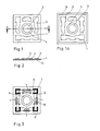
- Fig. 1 shows a plan view of the module interior facing top of a ceramic substrate 1, which can be inserted into a housing of the module known from DE-OS 30 28 178.
- the substrate 1 is preferably made of 96% Al2O3 and has an opening 2 in the middle for carrying out a fastening screw.
- Conductor tracks 3 and a reinforcing ring 4 according to the invention are arranged on the top of the substrate 1 and in the region of the opening 2.
- the width of the reinforcement ring 4 is, for example, 2 mm and corresponds approximately to a support surface 18 in a recess 17 of a central fastening part 13 of a housing 12, which is shown in FIG. 4.
- the distance of the reinforcement ring 4 to the inner metallization pattern, that is to say to the conductor tracks 3, is dimensioned such that the insulation resistance of the inner circuit to the outside to a heat sink is ensured after the module has been cast with casting compound.
- the distance between the reinforcing ring 4 and a copper layer 5 (see FIG. 2) on the underside of the ceramic substrate that is to say the distance between the thickness of the ceramic substrate Reinforcement ring 4 and copper layer 5 at the edge of the opening 2 generally cannot act as an insulation section, since the ceramic is not covered with potting compound at this point. Also between the outer edge of the ceramic substrate 1, on which an outer frame 14 of the housing 12 (see FIG. 6) is supported, and the conductor tracks 3, an insulation edge must be observed.
- the minimum distances to be maintained between metallization surfaces depend on the blocking voltages to be observed, on the insulation strength of the casting compound and finally on the resolution of the masking and etching technology used (e.g. screen printing process).
- the conductor tracks 3 and the reinforcement ring 4 on the upper side of the ceramic substrate 1 by direct connection (direct bonding method) of a 0.1 to 0.5 mm, preferably 0.3 mm thick copper foil to the ceramic substrate 1 This is done by using a film covering the entire surface of the top of the substrate 1, which is then etched.
- a copper foil is expediently used, which is approximately the same thickness as the foil used for the top-side metallization and into which a hole corresponding to the opening 2 has already been punched. The underside of the substrate 1 then no longer needs to be etched.
- the copper surfaces of the substrate metallized in this way are then appropriately chemically nickel-plated and prepared for the subsequent soldering process.
- FIG. 2 shows a section through the section plane AA of the substrate 1 entered in FIG. 1. From this it can be seen that on the underside of the ceramic substrate 1 a copper layer 5 is provided, which has approximately the same thickness as the reinforcing ring 4 and is also expediently connected directly to the substrate 1.
- the reinforcement ring 4 and the copper layer 5 have no electrical function. They serve only for mechanical reinforcement of the substrate 1 and, in their combination, bring about a significant reduction in the risk of breakage in comparison with the known substrate design.
- the invention can be applied in a corresponding manner for larger modules that are fastened with several screws.
- an outer reinforcement ring 6 can be provided on the ceramic substrate 1, which is designed and manufactured in the region of the opening 2 in the same way as the reinforcement ring 4. It may be necessary to increase the area of the ceramic substrate 1 somewhat, since certain distances between the conductor tracks 3 and the outer reinforcement ring 6 or the reinforcement ring 4 in the region of the opening 2 must be maintained with regard to the necessary insulation distances.
- the housing 12 in the region of its second bearing surface 18.1 in the second recess 17.1 of the frame 14 must be adapted accordingly (cf. FIG. 4 and the associated description).
- an outer reinforcement ring can also be provided on the substrate to protect a ceramic substrate inserted into the base surface.
- an outer reinforcement ring could advantageously be provided in a module according to DE-OS 31 27 457.
- FIG. 3 shows the upper side of the substrate 1 shown in FIGS. 1 and 2 after it has been soldered to placement elements.
- four diode chips 7, four copper clips 8 are soldered onto the ceramic substrate 1 as module-internal connecting elements between the anodes of the chips 7 and the conductor tracks 3 and four tabs 9 as external connections with a soft solder with a melting point around 300 ° C. without flux .
- the provided glass passivated diode chips 7 are soldered with the anodes upwards onto the substrate 1, so that the passivation area of the diodes 7 is at the top.
- planar passivated diode chips could also be used instead.
- FIG. 5 shows the individual parts that are required for producing the fully assembled substrate 1 shown in FIG. 3. From this it can be seen that the tabs 9 have an expansion curve 10 at their base and that the soft solder is advantageously applied as a solder foil 11.
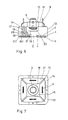
- the housing 12 has an outer frame 14 and a central fastening part 13, which is rigid with the frame 14 via ribs 15 connected is. It consists of a glass fiber reinforced plastic, which offers enough resistance to the pressure of a fastening screw even when heated to ensure fastening during many years of operation.
- the ribs 15 and the central fastening part 13 are designed so that they also act as extension paths to maintain the required creepage distances and clearances.
- the central fastening part 13 is therefore made relatively high, with a recess 16 for receiving the screw head.
- the central fastening part 13 has a recess 17 on its underside with a bearing surface 18 for the metallized substrate 1.
- the outer frame 14 of the housing 12 also has a second recess 17.1 on its underside with a second contact surface 18.1. In the second recess 17.1, a groove 19 is also provided for receiving excess adhesive.
- FIG. 6 shows a side view of the finished module after the assembled substrate 1 is glued into the housing 12 with an elastic, electrically insulating adhesive.
- the gluing point is both the contact surface 18 on the central fastening part 13 and the second contact surface 18.1 on the outer frame 14 of the housing 12.
- the elastic adhesive relieves the substrate 1 from the housing 12.
- the module is covered with a soft elastomeric casting compound 20 (preferably a silicone -Elastomer) of high purity, which protects the sensitive chips 7 (not visible in FIG. 6) and the soldered connections of the clips 8 from mechanical stresses.
- the above-mentioned high purity of the potting compound 20 is necessary in order to keep harmful ions away from the chips 7 and to ensure the insulation strength.
- the casting height is set so that completely immerse the expansion elbows 10 of the tabs 9 in the sealing compound 20.
- the module is filled with a thermosetting hard casting compound 21, preferably an epoxy resin, up to a fill level 22 below the upper edge of the outer frame 14 for sealing upwards.
- the tabs 9 are fixed in their position.
Abstract
Description
Die Erfindung bezieht sich auf ein Leistungshalbleitermodul mit einem Modulgehäuse und einem als Gehäuseboden eingesetzten Keramiksubstrat nach dem Oberbegriff des Anspruchs 1 und des Anspruchs 5. Zur Verbesserung der Wärmeabfuhr werden solche Module üblicherweise mit einem Kühlkörper in Kontakt gebracht, wofür in der Regel eine Schraubverbindung vorgesehen ist. Leistungshalbleitermodule mit Schraubbefestigung sind in unterschiedlicher Ausführung bekannt z.B. mit außen am Gehäuse angeformten Befestigungsflanschen oder bei rahmenförmigen Gehäusen auch mit einem zentralen Befestigungsteil, das zumindest eine Bohrung für eine Befestigungsschraube aufweist.The invention relates to a power semiconductor module with a module housing and a ceramic substrate used as the housing base according to the preamble of
Bei allen Ausführungsvarianten treten im Bereich der Befestigungsschrauben erhebliche mechanische Kräfte auf, die such über die im Schraubenbereich befindlichen Gehäuseteile auf das Keramiksubstrat übertragen. Die üblicherweise dünnen und spröden Keramiksubstrate sind daher in hohem Maße bruchgefährdet, insbesondere wenn das zulässige Drehmoment für die Schraubbefestigung über schritten wird. Es können Risse in der Keramik auftreten, die die Isolationsfestigkeit herabsetzen.In all variants, considerable mechanical forces occur in the area of the fastening screws, which are transmitted to the ceramic substrate via the housing parts located in the area of the screws. The usually thin and brittle ceramic substrates are therefore highly susceptible to breakage, especially if the permissible torque for the screw fastening exceeds is taken. Cracks can occur in the ceramic, which reduce the insulation strength.
Es sind bereits mehrere Vorschläge zur konstruktiven Gestaltung der Module bekanntgeworden, die eine Minderung der Bruchgefahr für das Keramiksubstrat bewirken. Trotzdem besteht weiterhin Bedarf an zusätzlichen oder alternativen Maßnahmen zum Schutz der bruchempfindlichen Keramiksubstrate.Several proposals for the structural design of the modules have already become known which reduce the risk of breakage for the ceramic substrate. Nevertheless, there is still a need for additional or alternative measures to protect the fragile ceramic substrates.
Aus der DE-OS 31 27 457 ist ein Leistungshalbleitermodul mit einem Keramiksubstrat als Gehäuseboden bekannt, bei dem das Substrat auf der Unterseite mit einer Kupferfolie versehen ist, und bei dem Flachstecker für Außenanschlüsse einen Dehnungsbogen aufweisen. Damit kann die Gefahr von Keramikbrüchen infolge unebener Kühlkörper bereits wesentlich reduziert werden. Belastungsprobleme durch Übertragung mechanischer Kräfte aus dem Bereich der Befestigungsschrauben sind jedoch damit noch nicht ausreichend gelöst.From DE-OS 31 27 457 a power semiconductor module with a ceramic substrate as the housing base is known, in which the substrate is provided on the underside with a copper foil, and in which the flat plug for external connections has an expansion curve. The risk of ceramic breaks due to uneven heat sinks can thus be significantly reduced. However, load problems caused by the transmission of mechanical forces from the area of the fastening screws have not yet been sufficiently solved.
Eine weitere wesentliche Verbesserung bringt der Vorschlag gemäß DE-OS 33 07 707, nämlich durch Schlitze im Kunststoffgehäuse die Übertragung mechanischer Spannungen zu verringern. Diese Maßnahme läßt sich jedoch nicht bei allen Modulkonstruktionen anwenden, zumindest nicht in einem solchen Umfang, daß eine Kraftübertragung völlig ausgeschlossen wäre. Kaum anwendbar sind solche Schlitze zur mechanischen Entkopplung beispielsweise bei einer Modulgestaltung gemäß DE-OS 30 28 178, nämlich einem Modul mit zentralem Befestigungsteil. Um einen gleichmäßigen Andruck des Moduls auf den Kühlkörper zu erreichen, soll nämlich das zentrale Befestigungsteil formstabil mit einem äußeren Rahmen verbunden sein.The proposal according to DE-OS 33 07 707 brings a further significant improvement, namely to reduce the transmission of mechanical stresses by means of slots in the plastic housing. However, this measure cannot be applied to all module constructions, at least not to such an extent that a power transmission would be completely excluded. Such slots for mechanical decoupling are hardly applicable, for example in a module design according to DE-OS 30 28 178, namely a module with a central fastening part. In order to achieve a uniform pressure of the module on the heat sink, the central fastening part should be connected to an outer frame in a dimensionally stable manner.
Der Erfindung liegt deshalb die Aufgabe zugrunde, für Leistungshalbleiter mit Kunststoffgehäuse und einem Boden aus einem Keramiksubstrat weitere Maßnahmen zur Minderung der Bruchgefahr anzugeben.The invention is therefore based on the object of specifying further measures for reducing the risk of breakage for power semiconductors with a plastic housing and a base made of a ceramic substrate.
Diese Aufgabe wird bei einem Leistungshalbleitermodul nach dem Oberbegriff des Anspruchs 1 durch dessen kennzeichnende Merkmale gelöst sowie bei einem Leistungshalbleitermodul nach dem Oberbegriff des Anspruchs 5 durch die kennzeichnenden Merkmale des Anspruchs 5. Vorteilhafte Ausgestaltungen sind in Unteransprüchen angegeben. Der Oberbegriff des Anspruchs 1 bezieht sich auf das aus der DE-OS 30 28 178 bekannte Modul, der Oberbegriff des Anspruchs 5 auf das aus der DE-OS 31 27 457 bekannte Modul.This object is achieved in a power semiconductor module according to the preamble of
Vorteile der Erfindung bestehen darin, daß die zur mechanischen Verstärkung vorgesehenen Metallisierungsflächen einfach und gleichzeitig mit den übrigen Metallisierungsflächen für elektrische Leitungen hergestellt werden können. Die Lösung ist bei unterschiedlichen Modulausführungen anwendbar. Das Keramiksubstrat kann mit hoher und gleichmäßiger Anpreßkraft auf einen Kühlkörper drücken und wird dabei wirksam vor Rißbildung geschützt.Advantages of the invention are that the metallization surfaces provided for mechanical reinforcement can be produced easily and simultaneously with the other metallization surfaces for electrical lines. The solution can be used for different module designs. The ceramic substrate can press on a heat sink with high and even contact pressure and is effectively protected against cracking.
Die Erfindung wird anhand eines in der Zeichnung dargestellten Ausführungsbeispiels näher erläutert.The invention is explained in more detail using an exemplary embodiment shown in the drawing.
Es zeigen:
- Fig. 1 eine Draufsicht auf ein Keramiksubstrat,
- Fig. 1a eine Ausführungsvariante des Keramiksubstrats,
- Fig. 2 einen Schnitt durch das in Fig. 1 dargestellte Substrat,
- Fig. 3 ein bestücktes Substrat,
- Fig. 4 einen Schnitt durch ein Kunststoffgehäuse mit zentralem Befestigungsteil,
- Fig. 5 eine Explosionsdarstellung der für das in Fig. 3 dargestellte Substrat benötigten Teile,
- Fig. 6 eine Seitenansicht eines fertiggestellten Leistungshalbleitermoduls,
- Fig. 7 eine Draufsicht auf das fertiggestellte Leistungshalbleitermodul.
- 1 is a plan view of a ceramic substrate,
- 1a shows a variant of the ceramic substrate,
- 2 shows a section through the substrate shown in FIG. 1,
- 3 shows an assembled substrate,
- 4 shows a section through a plastic housing with a central fastening part,
- 5 is an exploded view of the parts required for the substrate shown in FIG. 3;
- 6 shows a side view of a completed power semiconductor module,
- Fig. 7 is a plan view of the completed power semiconductor module.
Das Ausführungsbeispiel betrifft ein Leistungshalbleitermodul, das aus der DE-OS 30 28 178 bekannt ist. Das Leistungshalbleitermodul hat ein etwa quaderförmiges Kunststoffgehäuse mit einem zentralen Befestigungsteil und hat als Boden ein Keramiksubstrat. Das Modul stellt eine Realisierung einer ungesteuerten einphasigen Gleichrichterschaltung (Graetzbrücke) dar.The embodiment relates to a power semiconductor module, which is known from DE-OS 30 28 178. The power semiconductor module has an approximately cuboid plastic housing with a central fastening part and has a ceramic substrate as the bottom. The module represents an implementation of an uncontrolled single-phase rectifier circuit (Graetz bridge).
Fig. 1 zeigt eine Draufsicht auf die dem Modulinneren zugewandte Oberseite eines Keramiksubstrats 1, das in ein Gehäuse des aus der DE-OS 30 28 178 bekannten Moduls eingesetzt werden kann. Das Substrat 1 besteht vorzugsweise aus 96% Al₂O₃ und weist in der Mitte eine Öffnung 2 zur Durchführung einer Befestigungsschraube auf. Auf der Oberseite des Substrats 1 sind Leiterbahnen 3 sowie im Bereich der Öffnung 2 ein erfindungsgemäßer Verstärkungsring 4 angeordnet. Die Breite des Verstärkungsrings 4 beträgt z.B. 2 mm und entspricht etwa einer Auflagefläche 18 in einer Ausnehmung 17 eines zentralen Befestigungsteils 13 eines Gehäuses 12, das in Fig. 4 dargestellt ist. Der Abstand des Verstärkungsrings 4 zum inneren Metallisierungsmuster, also zu den Leiterbahnen 3, ist so bemessen, daß die Isolationsfestigkeit der inneren Schaltung nach außen zu einem Kühlkörper nach dem Vergießen des Moduls mit Vergußmasse gewährleistet ist. Es ist zu beachten, daß der Abstand zwischen dem Verstärkungsring 4 und einer Kupferschicht 5 (siehe Fig. 2) auf der Unterseite des Keramiksubstrats, also die durch die Dicke des Keramiksubstrats gegebene Strecke zwischen Verstärkungsring 4 und Kupferschicht 5 an der Kante der Öffnung 2 im allgemeinen nicht als Isolationsstrecke wirken kann, da die Keramik an dieser Stelle nicht mit Vergußmasse bedeckt ist. Auch zwischen dem Außenrand des Keramiksubstrats 1, auf den sich ein äußerer Rahmen 14 des Gehäuses 12 (siehe Fig. 6) abstützt und den Leiterbahnen 3 muß ein Isolationsrand eingehalten werden. Die minimalen Abstände, die zwischen Metallisierungsflächen (Leiterbahnen 3, Verstärkungsring 4) einzuhalten sind, richten sich nach den einzuhaltenden Sperrspannungen, nach der Isolationsfestigkeit der Vergußmasse und schließlich nach dem Auflösungsvermögen der angewendeten Maskier- und Ätztechnik (z.B. Siebdruckverfahren).Fig. 1 shows a plan view of the module interior facing top of a
Es ist zweckmäßig, die Leiterbahnen 3 und den Verstärkungsring 4 auf der Oberseite des Keramiksubstrats 1 herzustellen, durch direktes Verbinden (direct-bonding-Verfahren) einer 0,1 bis 0,5 mm, bevorzugt 0,3 mm dicken Kupferfolie mit dem Keramiksubstrat 1. Und zwar durch Verwendung einer ganzflächig die Oberseite des Substrats 1 bedeckenden Folie, die anschließend geätzt wird. Zur Herstellung der Kupferschicht 5 auf der Unterseite des Substrats 1 wird zweckmäßig eine Kupferfolie verwendet, die etwa gleich dick is wie die für die oberseitige Metallisierung benutzte Folie und in die bereits ein der Öffnung 2 entsprechendes Loch gestanzt ist. Die Unterseite des Substrats 1 braucht dann nicht mehr geätzt zu werden.It is expedient to produce the
Die Kupferflächen des so metallisierten Substrats werden anschließend zweckmäßig chemisch vernickelt und für den anschließenden Lötprozeß vorbereitet.The copper surfaces of the substrate metallized in this way are then appropriately chemically nickel-plated and prepared for the subsequent soldering process.
Fig. 2 zeigt einen Schnitt durch die in Fig. 1 eingetragene Schnittebene A-A des Substrats 1. Daraus ist ersichtlich, daß auf der Unterseite des Keramiksubstrats 1 eine Kupferschicht 5 vorgesehen ist, die etwa die gleiche Dicke wie der Verstärkungsring 4 hat und zweckmäßig ebenfalls direkt mit dem Substrat 1 verbunden ist. Der Verstärkungsring 4 und die Kupferschicht 5 haben keine elektrische Funktion. Sie dienen ausschließlich zur mechanischen Verstärkung des Substrats 1 und bewirken in ihrer Kombination eine wesentliche Herabsetzung der Bruchgefahr im Vergleich zur bekannten Substratausführung.FIG. 2 shows a section through the section plane AA of the
Selbstverständlich kann die Erfindung in entsprechender Weise für größere Module angewendet werden, die mit mehreren Schrauben befestigt werden.Of course, the invention can be applied in a corresponding manner for larger modules that are fastened with several screws.
Bei besonders formstabilen Kunststoffgehäusen, z.B. aus duroplastischen Polyestern mit Glasfaserverstärkung, kann es erforderlich sein, auch den äußeren Rand, auf dem das Gehäuse ebenfalls aufliegt, besonders zu schützen. Dazu kann, wie in Fig. 1a dargestellt, ein äußerer Verstärkungsring 6 auf dem Keramiksubstrat 1 vorgesehen werden, der in gleicher Weise wie der Verstärkungsring 4 im Bereich der Öffnung 2 gestaltet und hergestellt wird. Dabei kann es erforderlich sein, die Fläche des Keramiksubstrats 1 etwas zu vergrößern, da bestimmte Abstände zwischen den Leiterbahnen 3 und dem äußeren Verstärkungsring 6 bzw. dem Verstärkungsring 4 im Bereich der Öffnung 2 im Hinblick auf die notwendigen Isolationsstrecken einzuhalten sind. Selbstverständlich ist in diesem Fall das Gehäuse 12 im Bereich seiner zweiten Auflagefläche 18.1 in der zweiten Ausnehmung 17.1 des Rahmens 14 entsprechend anzupassen (vgl. Fig. 4 und zugehörige Beschreibung).In the case of particularly dimensionally stable plastic housings, for example made of thermosetting polyesters with glass fiber reinforcement, it may be necessary to also protect the outer edge on which the housing also rests. For this purpose, as shown in FIG. 1 a, an
Bei anderen Modulgestaltungen, die nicht in der Zeichnung dargestellt sind, also z.B. bei Verwendung eines Modulgehäuses mit außen angeformten Befestigungsflanschen, kann zum Schutz eines in die Bodenfläche eingesetzten Keramiksubstrats ebenfalls ein äußerer Verstärkungsring auf dem Substrat vorgesehen werden. Beispielsweise könnte ein solcher äußerer Verstärkungsring vorteilhaft bei einem Modul gemäß DE-OS 31 27 457 vorgesehen werden.For other module designs that are not shown in the drawing, e.g. when using a module housing with externally molded mounting flanges, an outer reinforcement ring can also be provided on the substrate to protect a ceramic substrate inserted into the base surface. For example, such an outer reinforcement ring could advantageously be provided in a module according to DE-OS 31 27 457.
Fig. 3 zeigt die Oberseite des in den Figuren 1 und 2 dargestellten Substrats 1, nachdem es mit Bestückungselementen verlötet ist. Zur Herstellung der dargestellten Gleichrichterschaltung werden auf das Keramiksubstrat 1 vier Diodenchips 7, vier Clips 8 aus Kupfer als modulinterne Verbindungselemente zwischen den Anoden der Chips 7 und den Leiterbahnen 3 und vier Flachstecker 9 als Außenanschlüsse mit einem Weichlot mit einem Schmelzpunkt um 300°C flußmittelfrei aufgelötet. Die vorgesehenen glaspassivierten Diodenchips 7 werden mit den Anoden nach oben auf das Substrat 1 gelötet, so daß der Passivierungsbereich der Dioden 7 oben liegt. Selbstverständlich könnten stattdessen auch planar passivierte Diodenchips verwendet werden.3 shows the upper side of the
Fig. 5 zeigt die einzelnen Teile, die zur Herstellung des in Fig. 3 dargestellten fertigbestückten Substrats 1 benötigt werden. Daraus ist ersichtlich, daß die Flachstecker 9 an ihrem Fußpunkt einen Dehnungsbogen 10 aufweisen und daß das Weichlot vorteilhaft als Lotfolie 11 aufgebracht wird.FIG. 5 shows the individual parts that are required for producing the fully assembled
Fig. 4 zeigt das Gehäuse 12, in das das fertiggelötete Substrat 1 eingeklebt wird. Das Gehäuse 12 weist einen äußeren Rahmen 14 und einen zentralen Befestigungsteil 13 auf, der über Rippen 15 starr mit dem Rahmen 14 verbunden ist. Es besteht aus einem glasfaserverstärkten Kunststoff, der dem Druck einer Befestigungsschraube auch bei Erwärmung ausreichend Widerstand bietet um die Befestigung während eines langjährigen Betriebes zu gewährleisten. Die Rippen 15 und der zentrale Befestigungsteil 13 sind so ausgeführt, daß sie zugleich als Verlängerungswege zur Einhaltung der erforderlichen Kriech- und Luftstrecken wirken. Das zentrale Befestigungsteil 13 ist deshalb relativ hoch ausgeführt, mit einer Vertiefung 16 zur Aufnahme des Schraubenkopfes.4 shows the
Das zentrale Befestigungsteil 13 weist auf seiner Unterseite eine Ausnehmung 17 mit einer Auflagefläche 18 für das metallisierte Substrat 1 auf. Auch der äußere Rahmen 14 des Gehäuses 12 weist auf seiner Unterseite eine zweite Ausnehmung 17.1 mit einer zweiten Auflagefläche 18.1 auf. In der zweiten Ausnehmung 17.1 ist außerdem eine Nut 19 zur Aufnahme von überschüssigem Klebstoff vorgesehen.The
Fig. 6 zeigt in Seitenansicht das fertige Modul nachdem das bestückte Substrat 1 in das Gehäuse 12 mit einem elastischen elektrisch isolierenden Klebstoff eingeklebt ist. Klebestelle ist sowohl die Auflagefläche 18 am zentralen Befestigungsteil 13 als auch die zweite Auflagefläche 18.1 am äußeren Rahmen 14 des Gehäuses 12. Bei Temperaturwechseln entlastet die elastische Klebung das Substrat 1 vom Gehäuse 12. Das Modul wird mit einer weichen elastomeren Vergußmasse 20 (vorzugsweise ein Silicon-Elastomer) hoher Reinheit vergossen, die die in Fig. 6 nicht sichtbaren empfindlichen Chips 7 und die Lötverbindungen der Clips 8 vor mechanischen Spannungen schützt. Die genannte hohe Reinheit der Vergußmasse 20 ist erforderlich um schädliche Ionen von den Chips 7 fernzuhalten und um die Isolationsfestigkeit sicherzustellen. Die Vergußhöhe wird dabei so eingestellt, daß die Dehnungsbogen 10 der Flachstecker 9 vollständig in die Vergußmasse 20 eintauchen. Schließlich wird das Modul mit einer duroplastischen Hartvergußmasse 21, vorzugsweise ein Epoxidharz, bis zu einer Füllhöhe 22 unterhalb der Oberkante des äußeren Rahmens 14 zur Abdichtung nach oben aufgefüllt. Dabei werden die Flachstecker 9 in ihrer Lage fixiert.6 shows a side view of the finished module after the assembled
Fig. 7 zeigt schließlich eine Draufsicht auf das fertige Modul. Die angegebenene Bezugszeichen sind bereits alle in der vorstehenden Beschreibung erwähnt.7 shows a top view of the finished module. The specified reference numerals have all already been mentioned in the above description.
Claims (5)
Priority Applications (1)
| Application Number | Priority Date | Filing Date | Title |
|---|---|---|---|
| AT87103618T ATE84378T1 (en) | 1986-03-26 | 1987-03-12 | POWER SEMICONDUCTOR MODULE. |
Applications Claiming Priority (2)
| Application Number | Priority Date | Filing Date | Title |
|---|---|---|---|
| DE3610288 | 1986-03-26 | ||
| DE19863610288 DE3610288A1 (en) | 1986-03-26 | 1986-03-26 | PERFORMANCE SEMICONDUCTOR MODULE |
Publications (3)
| Publication Number | Publication Date |
|---|---|
| EP0243637A2 true EP0243637A2 (en) | 1987-11-04 |
| EP0243637A3 EP0243637A3 (en) | 1990-05-16 |
| EP0243637B1 EP0243637B1 (en) | 1993-01-07 |
Family
ID=6297367
Family Applications (1)
| Application Number | Title | Priority Date | Filing Date |
|---|---|---|---|
| EP87103618A Expired - Lifetime EP0243637B1 (en) | 1986-03-26 | 1987-03-12 | Semi-conductor power module |
Country Status (3)
| Country | Link |
|---|---|
| EP (1) | EP0243637B1 (en) |
| AT (1) | ATE84378T1 (en) |
| DE (2) | DE3610288A1 (en) |
Cited By (3)
| Publication number | Priority date | Publication date | Assignee | Title |
|---|---|---|---|---|
| EP0391832A2 (en) * | 1989-04-05 | 1990-10-10 | Fagor, S.Coop. Ltda. | Improvements in the construction of bridge rectifiers |
| GB2241110A (en) * | 1990-02-19 | 1991-08-21 | Mitsubishi Electric Corp | Semiconductor package |
| EP0505193A1 (en) * | 1991-03-21 | 1992-09-23 | Harris Corporation | Cover for electrical components package |
Families Citing this family (8)
| Publication number | Priority date | Publication date | Assignee | Title |
|---|---|---|---|---|
| DE3837920A1 (en) * | 1988-11-09 | 1990-05-10 | Semikron Elektronik Gmbh | SEMICONDUCTOR ELEMENT |
| JPH05166969A (en) * | 1991-10-14 | 1993-07-02 | Fuji Electric Co Ltd | Semiconductor device |
| DE4300516C2 (en) * | 1993-01-12 | 2001-05-17 | Ixys Semiconductor Gmbh | Power semiconductor module |
| EP0671766A1 (en) * | 1994-02-25 | 1995-09-13 | Harris Corporation | Semiconductor package and method |
| DE4407810C2 (en) * | 1994-03-09 | 1998-02-26 | Semikron Elektronik Gmbh | Circuit arrangement (module) |
| DE102004035746B4 (en) * | 2004-07-23 | 2009-04-16 | Infineon Technologies Ag | The power semiconductor module |
| DE102006005445A1 (en) * | 2006-02-07 | 2007-08-16 | Semikron Elektronik Gmbh & Co. Kg | The power semiconductor module |
| CN102013578B (en) * | 2009-09-07 | 2014-05-28 | 比亚迪股份有限公司 | Conductor extraction structure and power module |
Citations (5)
| Publication number | Priority date | Publication date | Assignee | Title |
|---|---|---|---|---|
| DE3028178A1 (en) * | 1980-07-25 | 1982-02-25 | Brown, Boveri & Cie Ag, 6800 Mannheim | PERFORMANCE SEMICONDUCTOR MODULE |
| US4367523A (en) * | 1981-02-17 | 1983-01-04 | Electronic Devices, Inc. | Rectifier bridge unit |
| EP0069901A2 (en) * | 1981-07-11 | 1983-01-19 | BROWN, BOVERI & CIE Aktiengesellschaft | Current rectifier module |
| FR2535898A3 (en) * | 1982-11-10 | 1984-05-11 | Bbc Brown Boveri & Cie | Power transistor module for rectifying equipment |
| DE3323246A1 (en) * | 1983-06-28 | 1985-01-10 | Brown, Boveri & Cie Ag, 6800 Mannheim | Power semiconductor module |
Family Cites Families (3)
| Publication number | Priority date | Publication date | Assignee | Title |
|---|---|---|---|---|
| DE1861572U (en) * | 1962-08-17 | 1962-11-08 | Steatit Magnesia Ag | DISC-SHAPED COMPONENT FOR COMMUNICATION TECHNOLOGY OR SIMILAR DEVICES. |
| DE3241509A1 (en) * | 1982-11-10 | 1984-05-10 | Brown, Boveri & Cie Ag, 6800 Mannheim | POWER TRANSISTOR MODULE |
| DE3307704C2 (en) * | 1983-03-04 | 1986-10-23 | Brown, Boveri & Cie Ag, 6800 Mannheim | Converter module with fastening straps |
-
1986
- 1986-03-26 DE DE19863610288 patent/DE3610288A1/en not_active Withdrawn
-
1987
- 1987-03-12 DE DE8787103618T patent/DE3783385D1/en not_active Expired - Lifetime
- 1987-03-12 EP EP87103618A patent/EP0243637B1/en not_active Expired - Lifetime
- 1987-03-12 AT AT87103618T patent/ATE84378T1/en active
Patent Citations (5)
| Publication number | Priority date | Publication date | Assignee | Title |
|---|---|---|---|---|
| DE3028178A1 (en) * | 1980-07-25 | 1982-02-25 | Brown, Boveri & Cie Ag, 6800 Mannheim | PERFORMANCE SEMICONDUCTOR MODULE |
| US4367523A (en) * | 1981-02-17 | 1983-01-04 | Electronic Devices, Inc. | Rectifier bridge unit |
| EP0069901A2 (en) * | 1981-07-11 | 1983-01-19 | BROWN, BOVERI & CIE Aktiengesellschaft | Current rectifier module |
| FR2535898A3 (en) * | 1982-11-10 | 1984-05-11 | Bbc Brown Boveri & Cie | Power transistor module for rectifying equipment |
| DE3323246A1 (en) * | 1983-06-28 | 1985-01-10 | Brown, Boveri & Cie Ag, 6800 Mannheim | Power semiconductor module |
Non-Patent Citations (2)
| Title |
|---|
| (ELECTRONIC COMPONENTS & APPLICATIONS) * |
| (ELECTRONIC COMPONENTS & APPLICATIONS) Band 7, Nr. 4, 1985, Seiten 250-255, Eindhoven, NL; "Insulated encapsulations for easier mointing of power semiconductors" * |
Cited By (6)
| Publication number | Priority date | Publication date | Assignee | Title |
|---|---|---|---|---|
| EP0391832A2 (en) * | 1989-04-05 | 1990-10-10 | Fagor, S.Coop. Ltda. | Improvements in the construction of bridge rectifiers |
| EP0391832A3 (en) * | 1989-04-05 | 1991-06-05 | Fagor, S.Coop. Ltda. | Improvements in the construction of bridge rectifiers |
| GB2241110A (en) * | 1990-02-19 | 1991-08-21 | Mitsubishi Electric Corp | Semiconductor package |
| US5068156A (en) * | 1990-02-19 | 1991-11-26 | Mitsubishi Denki Kabushiki Kaisha | Semiconductor package |
| GB2241110B (en) * | 1990-02-19 | 1993-12-15 | Mitsubishi Electric Corp | Semiconductor package |
| EP0505193A1 (en) * | 1991-03-21 | 1992-09-23 | Harris Corporation | Cover for electrical components package |
Also Published As
| Publication number | Publication date |
|---|---|
| EP0243637B1 (en) | 1993-01-07 |
| DE3783385D1 (en) | 1993-02-18 |
| DE3610288A1 (en) | 1987-10-01 |
| EP0243637A3 (en) | 1990-05-16 |
| ATE84378T1 (en) | 1993-01-15 |
Similar Documents
| Publication | Publication Date | Title |
|---|---|---|
| EP0205746B1 (en) | Semiconductor power module comprising a ceramic substrate | |
| EP1547166B1 (en) | Light source module and method for production thereof | |
| EP1982355B1 (en) | Power electronics assembly | |
| DE19921109B4 (en) | Electronic component and electronic component with a ceramic component element | |
| EP1255299B1 (en) | Power semiconductor device with pressure contact | |
| EP2422367B1 (en) | Encapsulated circuit device for substrates with absorption layer and method for producing the same | |
| DE102014213564B4 (en) | Semiconductor device and method for manufacturing the same | |
| DE69735361T2 (en) | Resin-encapsulated semi-conductor arrangement and method of production therefor | |
| DE4418426B4 (en) | Semiconductor power module and method of manufacturing the semiconductor power module | |
| DE10013255B4 (en) | Resin encapsulated electronic device for use in internal combustion engines | |
| DE102007017831B4 (en) | Semiconductor module and a method for producing a semiconductor module | |
| EP0237739A2 (en) | Semiconductor power module and method of producing the module | |
| DE102013226544B4 (en) | Semiconductor device | |
| DE10251248A1 (en) | Power semiconductor device | |
| DE10031678A1 (en) | Power semiconductor module has intermediate connection terminal and connection piece for providing releasable connection between control semiconductor element and power semiconductor | |
| DE3508456A1 (en) | Power semiconductor module | |
| DE19926756A1 (en) | Electronic circuit housing with improved heat dissipation for e.g. rectifiers in automobile circuits | |
| DE19634202C2 (en) | Semiconductor device | |
| DE10222608B4 (en) | Semiconductor device and method for manufacturing the same | |
| DE69923374T2 (en) | Semiconductor device | |
| EP0243637B1 (en) | Semi-conductor power module | |
| EP0124029A2 (en) | Well-coolable modular circuit carrying an electrical component | |
| DE10162749A1 (en) | circuitry | |
| EP0718886A1 (en) | Semiconductor power module | |
| DE102015115122A1 (en) | Power semiconductor module with two-part housing |
Legal Events
| Date | Code | Title | Description |
|---|---|---|---|
| PUAI | Public reference made under article 153(3) epc to a published international application that has entered the european phase |
Free format text: ORIGINAL CODE: 0009012 |
|
| AK | Designated contracting states |
Kind code of ref document: A2 Designated state(s): AT CH DE FR GB IT LI NL SE |
|
| RAP1 | Party data changed (applicant data changed or rights of an application transferred) |
Owner name: ASEA BROWN BOVERI AKTIENGESELLSCHAFT |
|
| PUAL | Search report despatched |
Free format text: ORIGINAL CODE: 0009013 |
|
| AK | Designated contracting states |
Kind code of ref document: A3 Designated state(s): AT CH DE FR GB IT LI NL SE |
|
| 17P | Request for examination filed |
Effective date: 19900622 |
|
| 17Q | First examination report despatched |
Effective date: 19910627 |
|
| GRAA | (expected) grant |
Free format text: ORIGINAL CODE: 0009210 |
|
| AK | Designated contracting states |
Kind code of ref document: B1 Designated state(s): AT CH DE FR GB IT LI NL SE |
|
| PG25 | Lapsed in a contracting state [announced via postgrant information from national office to epo] |
Ref country code: SE Effective date: 19930107 Ref country code: NL Effective date: 19930107 |
|
| REF | Corresponds to: |
Ref document number: 84378 Country of ref document: AT Date of ref document: 19930115 Kind code of ref document: T |
|
| PGFP | Annual fee paid to national office [announced via postgrant information from national office to epo] |
Ref country code: AT Payment date: 19930216 Year of fee payment: 7 |
|
| REF | Corresponds to: |
Ref document number: 3783385 Country of ref document: DE Date of ref document: 19930218 |
|
| GBT | Gb: translation of ep patent filed (gb section 77(6)(a)/1977) |
Effective date: 19930122 |
|
| ET | Fr: translation filed | ||
| ITF | It: translation for a ep patent filed |
Owner name: DE DOMINICIS & MAYER S.R.L. |
|
| PG25 | Lapsed in a contracting state [announced via postgrant information from national office to epo] |
Ref country code: LI Effective date: 19930331 Ref country code: CH Effective date: 19930331 |
|
| NLV1 | Nl: lapsed or annulled due to failure to fulfill the requirements of art. 29p and 29m of the patents act | ||
| PLBE | No opposition filed within time limit |
Free format text: ORIGINAL CODE: 0009261 |
|
| STAA | Information on the status of an ep patent application or granted ep patent |
Free format text: STATUS: NO OPPOSITION FILED WITHIN TIME LIMIT |
|
| REG | Reference to a national code |
Ref country code: CH Ref legal event code: PL |
|
| 26N | No opposition filed | ||
| PG25 | Lapsed in a contracting state [announced via postgrant information from national office to epo] |
Ref country code: AT Effective date: 19940312 |
|
| PGFP | Annual fee paid to national office [announced via postgrant information from national office to epo] |
Ref country code: GB Payment date: 19961217 Year of fee payment: 11 |
|
| PG25 | Lapsed in a contracting state [announced via postgrant information from national office to epo] |
Ref country code: GB Free format text: LAPSE BECAUSE OF NON-PAYMENT OF DUE FEES Effective date: 19980312 |
|
| GBPC | Gb: european patent ceased through non-payment of renewal fee |
Effective date: 19980312 |
|
| PGFP | Annual fee paid to national office [announced via postgrant information from national office to epo] |
Ref country code: FR Payment date: 20060317 Year of fee payment: 20 |
|
| PGFP | Annual fee paid to national office [announced via postgrant information from national office to epo] |
Ref country code: IT Payment date: 20060331 Year of fee payment: 20 |
|
| PGFP | Annual fee paid to national office [announced via postgrant information from national office to epo] |
Ref country code: DE Payment date: 20060419 Year of fee payment: 20 |