EP0246433A1 - Current attenuator useful in a very low leakage current measuring device - Google Patents
Current attenuator useful in a very low leakage current measuring device Download PDFInfo
- Publication number
- EP0246433A1 EP0246433A1 EP87104936A EP87104936A EP0246433A1 EP 0246433 A1 EP0246433 A1 EP 0246433A1 EP 87104936 A EP87104936 A EP 87104936A EP 87104936 A EP87104936 A EP 87104936A EP 0246433 A1 EP0246433 A1 EP 0246433A1
- Authority
- EP
- European Patent Office
- Prior art keywords
- current
- output
- attenuator
- divider
- coupled
- Prior art date
- Legal status (The legal status is an assumption and is not a legal conclusion. Google has not performed a legal analysis and makes no representation as to the accuracy of the status listed.)
- Granted
Links
- 238000012360 testing method Methods 0.000 claims abstract description 24
- 239000004065 semiconductor Substances 0.000 claims description 24
- 239000000758 substrate Substances 0.000 claims description 11
- 230000008878 coupling Effects 0.000 claims description 6
- 238000010168 coupling process Methods 0.000 claims description 6
- 238000005859 coupling reaction Methods 0.000 claims description 6
- 239000000463 material Substances 0.000 claims description 3
- 230000004044 response Effects 0.000 claims description 2
- 230000002238 attenuated effect Effects 0.000 abstract description 2
- 239000002184 metal Substances 0.000 description 10
- 238000004519 manufacturing process Methods 0.000 description 9
- 230000004888 barrier function Effects 0.000 description 8
- 208000032750 Device leakage Diseases 0.000 description 5
- 238000013461 design Methods 0.000 description 5
- 238000010586 diagram Methods 0.000 description 5
- 238000009826 distribution Methods 0.000 description 5
- 238000000034 method Methods 0.000 description 4
- 238000000151 deposition Methods 0.000 description 3
- VYPSYNLAJGMNEJ-UHFFFAOYSA-N Silicium dioxide Chemical compound O=[Si]=O VYPSYNLAJGMNEJ-UHFFFAOYSA-N 0.000 description 2
- 230000008021 deposition Effects 0.000 description 2
- 238000005259 measurement Methods 0.000 description 2
- 239000000523 sample Substances 0.000 description 2
- 229910052581 Si3N4 Inorganic materials 0.000 description 1
- 230000009471 action Effects 0.000 description 1
- 230000002411 adverse Effects 0.000 description 1
- 238000013459 approach Methods 0.000 description 1
- 230000008859 change Effects 0.000 description 1
- 239000004020 conductor Substances 0.000 description 1
- 230000007547 defect Effects 0.000 description 1
- 238000009792 diffusion process Methods 0.000 description 1
- 230000005669 field effect Effects 0.000 description 1
- 238000002513 implantation Methods 0.000 description 1
- 239000011810 insulating material Substances 0.000 description 1
- 238000009413 insulation Methods 0.000 description 1
- 239000012212 insulator Substances 0.000 description 1
- 238000002955 isolation Methods 0.000 description 1
- 238000000691 measurement method Methods 0.000 description 1
- 238000012986 modification Methods 0.000 description 1
- 230000004048 modification Effects 0.000 description 1
- 230000010355 oscillation Effects 0.000 description 1
- 230000008569 process Effects 0.000 description 1
- 238000012545 processing Methods 0.000 description 1
- 235000012239 silicon dioxide Nutrition 0.000 description 1
- 239000000377 silicon dioxide Substances 0.000 description 1
- HQVNEWCFYHHQES-UHFFFAOYSA-N silicon nitride Chemical compound N12[Si]34N5[Si]62N3[Si]51N64 HQVNEWCFYHHQES-UHFFFAOYSA-N 0.000 description 1
Images

Classifications
-
- G—PHYSICS
- G01—MEASURING; TESTING
- G01R—MEASURING ELECTRIC VARIABLES; MEASURING MAGNETIC VARIABLES
- G01R31/00—Arrangements for testing electric properties; Arrangements for locating electric faults; Arrangements for electrical testing characterised by what is being tested not provided for elsewhere
- G01R31/26—Testing of individual semiconductor devices
- G01R31/2607—Circuits therefor
- G01R31/2632—Circuits therefor for testing diodes
-
- G—PHYSICS
- G01—MEASURING; TESTING
- G01R—MEASURING ELECTRIC VARIABLES; MEASURING MAGNETIC VARIABLES
- G01R19/00—Arrangements for measuring currents or voltages or for indicating presence or sign thereof
- G01R19/0092—Arrangements for measuring currents or voltages or for indicating presence or sign thereof measuring current only
Definitions
- This invention relates to an attenuator useful in a current measuring circuit and more particularly to a precision current attenuator useable in a current measuring device which can extend the practical testing range of current measuring devices used in automatic testers from the microampere range to the picoampere range.
- the memory cells are designed so that the standby currents are the minimum necessary to retain data stored therein. This results in a cell being sensitive to low level currents at cell nodes to which devices at low forward bias and reverse bias are connected. If these low level currents exceed the limits assumed in the design, the cell will fail. Such failures can substantially reduce the number of functional chips yielded by the manufacturing process.
- a VLSI semiconductor chip contains hundreds of thousands of devices. When such a chip must operate at low power, it is essential that the discrete device leakage current distribution be accurately known. This is necessary so that the circuits can be designed to tolerate the worst case leakage which can occur.
- Schottky barrier diode SBD
- a Schottky barrier diode is typically formed by depositing a metal over an etched opening in the top insulating layer of the semiconductor wafer.
- the mean leakage current of such a device is in the sub-picoampere range, the upper bound of the leakage current distribution can be considerably higher, e.g., in the nanoampere range.
- a large number of discrete devices must be measured. This measurement must be periodically done during high volume manufacture of the chip so that if the upper bound increases, corrective action can be taken to reduce leakage and maintain the desired level of manufacturing yield.
- High volume manufactured semiconductor chips are typically tested by automatic electrical testers which step probes from chip site to chip site over the semiconductor wafer. The measured data is automatically sent to and stored in a host computer.
- Such testers can measure currents accurately in the micro ampere range and possibly down to 100 nanoampere but not in the sub-nanoampere range. Therefore, such currently available testers cannot be used to measure the upper bound of a leakage current distribution in a discrete device such as a Schottky barrier diode. Using other measurement techniques to measure this distribution upper bound of leakage current for a Schottky barrier diode, however, is not sufficiently fast so as to be suitable for use in a high volume manufacturing environment. Accordingly, the prior art testers and methods do not provide any means for measuring leakage current in the sub-nanoampere range in a high volume manufacturing environment for semiconductor devices.
- Typical low current measuring devices used in the laboratory may be used to measure currents in the picoampere range. These measuring devices when used to measure low currents in a circuit on a chip are quite difficult to use because the probe capacitance and the like cause the device to respond very slowly. Hence, this approach is not suitable for use in a manufacturing testing environment where such current measurements have to be made quickly and accurately.
- the current invention comprises a specially designed current attenuator with extremely low leakage currents.
- the attenuator in its intended use in a precision low current measuring device is coupled to the device under test and to a differential amplifier.
- the differential amplifier output is utilized by a conventional current measuring device to measure the current therethrough which is related to the current passing through the device under test by the amount of attenuation provided by the attenuator.
- the attenuator of the present invention includes a plurality of stages coupled in cascade. Each stage includes an input terminal for receiving current and an output terminal. Disposed between the input and output terminals is a specially designed current divider means which divides the input current thereto into n known parts where n is an integer greater than or equal to 2. Coupling means are provided to couple m of the known current parts to the stage output where m is a number greater than or equal to 1 and less than or equal to n - 1. By expeditiously selecting the number n and m, and the number of attenuator stages, it is a possible to attenuate the current input to the the stage by a selected amount.
- a device or circuit under test is coupled to the output of the attenuator.
- a differential amplifier is also coupled to the attenuator output.
- the differential amplifier itself has an output which couples to the input of the attenuator.
- the differential amplifier provides an input current to the attenuator which is attenuated by a known amount and becomes, at its output, a current equal to the current which is intended to be measured such as the leakage current through a Schottky barrier diode.
- the current passing through the differential amplifier can be measured by conventional current measuring apparatus with the actual leakage current being determined by dividing the measured current by the amount of attenuation provided by the attenuator circuit.
- the circuits utilized in the attenuator and the differential amplifier of the current measuring devices according to the present invention include semiconductor elements consisting only of PN junctions to form PNP transistors and two P-channel insulated gate field effect transistors (PFETs).
- the PN junctions are formed from the base-collector junctions of a conventional vertical NPN bipolar transistor.
- the emitter-base P-N junction of such transistor is not used as the leakage current can be unacceptably high.
- Each PFET is made of a metal gate over an N-region between two P-base regions of a conventional NPN transistor. Accordingly, the current measuring circuit of the present invention can be manufactured using a conventional bipolar process without the need for any additional process steps.
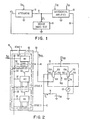
- the attenuator circuit of the present invention is illustrated in block diagram fashion in a configuration utilized for measuring currents in the picoampere range.
- the current measuring circuit includes the attenuator 10 which has a bias current input thereto as indicated by the arrow IB1.
- the output of the attenuator 10 is coupled by the wire 12 to the circuit or device under test 14 and also an input to the differential amplifier 16.
- a bias includes a plurality of intermediate output terminals 54 which are all coupled together.
- a further intermediate output terminal 56 is not coupled to the other intermediate output terminals but is coupled to the input terminal to the next stage of the attenuator 10.
- the current attenuator means M1 is designed in such a fashion that the current input thereto through the lead 52 is divided into n equal or known number of parts where n comprises the number of intermediate output terminals from the current divider means M1.
- the current divider means M1 includes 10 intermediate output terminals and, accordingly, the current entering the current divider means via lead 52 is divided into 10 equal parts.
- the current attenuator first stage accordingly, has maximum attenuation when only 1 of the intermediate output terminals is connected to the input of the next attenuator stage. In the present circuit as illustrated in Fig.
- the current passing through the output terminal 56 and comprising the input to stage 2 is one-tenth of the current entering via the connector lead 52 into stage 1.
- the current divider means M1 includes 10 intermediate output terminals, although , for ease of illustration, only 6 such intermediate output terminals are illustrated.
- the second attenuator stage includes a current divider means M2 which is functionally the same as M1 and it also divides the current input thereto into n equal or known number of parts with one such part being directed to the input of a third attenuator stage.
- the third attenuator stage includes a current divider means M3 which is functionally the same as M1 and also divides the current input thereto into n equal or known number parts.
- one of the intermediate outputs from the current divider means M3 comprises the output of the current attenuator 10 and is coupled to the line 12 which in turn couples to the device under test 14 and to an input to the differential amplifier 16. It should be noted that the number n of intermediate output terminals in each stage can be different from the number of intermediate output terminals in each other stage.
- a diode 64 is coupled between the point 58 and the lead 60 which produces a further voltage drop in the range of between about 0.7 and 0.8 volts. As such, the voltage at the lead 60 is approximately between 0.7 and 0.8 volts below the voltage at the input terminal 62.
- a further diode 66 is coupled between lead 60 and the lead 68 to thereby establish the voltage at lead 68 at between about 0.7 and 0.8 volts below the voltage at the input terminal 70 to stage 3 of the attenuator 10.
- Each of the current attenuator means M1, M2 and M3 of Fig. 2 are constructed in a manner illustrated by Figs. 3 and 5 and has an equivalent circuit as illustrated in Fig. 4.
- each stage of the attenuator is made up of 10 lateral PNP transistors shown in its equivalent form in Fig. 4 as T1 through T10.
- Each PNP transistor is of the same design and physical configuration and is formed in a single isolation region 100 as illustrated in Fig. 3.
- the tenth collector is brought out separately via a metal line 104 which comprises a stage output terminal.
- the particular collectors which are selected to be coupled together is not critical as any nine collectors could have been selected.
- a common emitter formed, in the preferred embodiment, by a single Pregion 106 which is brought out of the chip via a metal line 108.
- the configuration also includes a common base 110 which is brought out of the chip via metal line 112.
- Fig. 5 illustrates the fabrication of the device as taken along section line A-A of Fig. 3, the device is manufactured on a P substrate material.
- a subcollector region 110 having a doping of N+ is either diffused or implanted into the surface of the P substrate 111.
- an N doped region 113 is formed over the substrate 110 with the N+ region therein by means of, for example, epitaxial deposition. Due to subsequent processing and heat, the N+ region, which originally was formed in the P substrate 111, diffuses into the epitaxially deposited N region 113 so that it ultimately occupies the horizontally disposed Nregion such as that labelled 110 in Fig. 5.
- a vertically disposed N+ region 115 is formed either by diffusion or by implantation to thereby form a continuous Ndoped region to which a metal connector lead 112 can be attached.
- the N+ region thus formed comprises a means to connect to the base region 113.
- the connector lead 112 comprises the base contact to the PNP transistor illustrated in Fig. 5.
- the collector C10 comprises a P region which has been either diffused or implanted into the N region 113.
- the emitter 106 also comprises a P doped region which is either diffused or implanted into the N region 113.
- the collector C10 is electrically connected by a metal conductor lead 104 and the emitter 106 is connected by a metal connector 108.
- the metal connectors 104, 108 and 112 provide a means for electrically connecting the PNP transistor to other circuits.
- An insulating layer 120 is formed on the surface of the N region 113 to provide insulation between the electrical connector leads 104, 108 and 112 and to protect the substrate.
- the insulator layer 120 preferably comprises an oxide layer such as silicon dioxide, and a layer over that of silicon nitride although other insulating materials might also be utilized.
- current flows out of the drain of PFET 150 or 152 depends on the relative potentials of the gates 166 and 164, the latter of which is held at ground potential. If the gate 166 were also at ground potential, the current forced into the two sources 154 and 156 would divide equally between the two PFETs 150 and 152. In general during actual operation of the circuit, the voltage on the gate 166 will be different from ground potential and this difference will cause a change in the current flowing out of the drain 168 as compared to that flowing out of the drain 162.
- the current attenuator operates in conjunction with the differential amplifier to measure device leakage current in the following manner.
- no current flows into or out of the gate 166 of PFET 150. Consequently, any current flowing in the lead 12 corresponds to the leakage current through the device under test 14.
- the current flowing from the drain 168 to the attenuator is equal to KIL where K is the attenuation of the current attenuator according to the present invention.
- K is the attenuation of the current attenuator according to the present invention.
- the attenuator of Fig. 2 is designed to produce an output current which is one-thousand times smaller than its input current, the value of K for this circuit is one-thousand.
- the bias current IB3 is a known current and the current flowing from the drain 162 is measured by a microammeter 20, the current in the drain 168 can thereby be calculated and is equal to IB3 minus the measured current IM.
- This current is equal to a current which is one-thousand times greater , for the illustrated configuration, than the leakage current of the device under test 14.
- this leakage current may be very small which is the case for, for example, Schottky barrier diodes, it may prove necessary to have a current attenuator 10 having more stages than the circuit illustrated in Fig. 2.
Abstract
Description
- This invention relates to an attenuator useful in a current measuring circuit and more particularly to a precision current attenuator useable in a current measuring device which can extend the practical testing range of current measuring devices used in automatic testers from the microampere range to the picoampere range.
- In the semiconductor fabrication art, there is an increasing necessity for devices which have very low leakage currents in both logic and in memory circuits. The increased density of both logic and memory chips has produced the consequent need to maintain these chips at a level of power dissipation which can be cooled economically. This requires the circuits used to have a low power dissipation. Such lower power circuits are generally achieved by designing circuits to operate at currents lower than previous generation circuits. This low operating current requirement, however, makes it necessary to measure more accurately the distribution of discrete device leakage currents both in the forward and in the reverse mode of operation as the leakage current can be large enough to adversely affect circuit operation.
- In the field of semiconductor device design and manufacture, such devices must be tested to determine whether their electrical parameters meet design specifications or to determine whether the device has defects. Semiconductor circuits are designed assuming that the electrical characteristics of the component devices will fall within certain specified ranges. When a device characteristic deviates from this assumed specification, however, the circuit will fail. With the increased density of both semiconductor logic and memory chips, the need to maintain chip power dissipation within a range which can be economically cooled requires circuits that are designed to operate at very low power dissipation levels. For example, for a high density semiconductor memory chip to maintain low chip power dissipation, it is desirable that all memory cells on the chip which are in standby condition, that is in the condition when data is neither being written into nor read therefrom, should consume the minimum power which the semiconductor design will allow. To achieve this, the memory cells are designed so that the standby currents are the minimum necessary to retain data stored therein. This results in a cell being sensitive to low level currents at cell nodes to which devices at low forward bias and reverse bias are connected. If these low level currents exceed the limits assumed in the design, the cell will fail. Such failures can substantially reduce the number of functional chips yielded by the manufacturing process.
- A VLSI semiconductor chip contains hundreds of thousands of devices. When such a chip must operate at low power, it is essential that the discrete device leakage current distribution be accurately known. This is necessary so that the circuits can be designed to tolerate the worst case leakage which can occur.
- One type of device for which leakage current is desired to be measured is the Schottky barrier diode (SBD) which is commonly used in both logic and memory circuits. A Schottky barrier diode is typically formed by depositing a metal over an etched opening in the top insulating layer of the semiconductor wafer. Although the mean leakage current of such a device is in the sub-picoampere range, the upper bound of the leakage current distribution can be considerably higher, e.g., in the nanoampere range. To obtain an accurate determination of the upper bound of the leakage current for Schottky barrier diodes on a chip, a large number of discrete devices must be measured. This measurement must be periodically done during high volume manufacture of the chip so that if the upper bound increases, corrective action can be taken to reduce leakage and maintain the desired level of manufacturing yield.
- High volume manufactured semiconductor chips are typically tested by automatic electrical testers which step probes from chip site to chip site over the semiconductor wafer. The measured data is automatically sent to and stored in a host computer. Such testers can measure currents accurately in the micro ampere range and possibly down to 100 nanoampere but not in the sub-nanoampere range. Therefore, such currently available testers cannot be used to measure the upper bound of a leakage current distribution in a discrete device such as a Schottky barrier diode. Using other measurement techniques to measure this distribution upper bound of leakage current for a Schottky barrier diode, however, is not sufficiently fast so as to be suitable for use in a high volume manufacturing environment. Accordingly, the prior art testers and methods do not provide any means for measuring leakage current in the sub-nanoampere range in a high volume manufacturing environment for semiconductor devices.
- Various devices are known in the prior art for measuring low currents. For example, a circuit for doing so is described and claimed in the patent of McPhail, US Patent No. 3,702,967 entitled "Electronic Test System Operable in Two Modes". This patent describes a circuit making a parametric test system that can provide a forcing current at a predetermined level in one mode with a voltage being measured or a forcing voltage of a constant potential in another mode with a current being measured. The circuit does not provide any means to extend the range of conventional automatic testers to measure leakage currents in the sub-nanoampere range.
- Another circuit for measuring P-N junction device leakage is described and claimed in the patent of Verkuil, US Patent Re. 29,918 entitled "Contactless LSI Junction Leakage Testing Method", reissued on February 20, 1979. This patent describes a circuit for contactless measuring P-N junction leakage currents by inductively coupling high frequency oscillations to a semiconductor specimen which is simultaneously subjected to a pulsed light of selected intensity. The described circuit does not measure discrete device leakage current in response to a fixed applied DC voltage nor does it measure currents in the sub-nanoampere range.
- Typical low current measuring devices used in the laboratory may be used to measure currents in the picoampere range. These measuring devices when used to measure low currents in a circuit on a chip are quite difficult to use because the probe capacitance and the like cause the device to respond very slowly. Hence, this approach is not suitable for use in a manufacturing testing environment where such current measurements have to be made quickly and accurately.
- It is a principle object of the present invention to provide means for extending the current measuring range of conventional automatic semiconductor device testers to the picoampere range.
- It is another object of the present invention to provide a current measuring circuit operative in the picoampere range which utilizes a circuit that can be integrated with the semiconductor device under test without requiring an additional or special process steps.
- It is another principle object of the present invention to provide a current attenuator circuit for very accurately attenuating an input current thereto by an exact amount.
- The current invention comprises a specially designed current attenuator with extremely low leakage currents. The attenuator, in its intended use in a precision low current measuring device is coupled to the device under test and to a differential amplifier. The differential amplifier output is utilized by a conventional current measuring device to measure the current therethrough which is related to the current passing through the device under test by the amount of attenuation provided by the attenuator.
- The attenuator of the present invention includes a plurality of stages coupled in cascade. Each stage includes an input terminal for receiving current and an output terminal. Disposed between the input and output terminals is a specially designed current divider means which divides the input current thereto into n known parts where n is an integer greater than or equal to 2. Coupling means are provided to couple m of the known current parts to the stage output where m is a number greater than or equal to 1 and less than or equal to n - 1. By expeditiously selecting the number n and m, and the number of attenuator stages, it is a possible to attenuate the current input to the the stage by a selected amount.
- In an application for the current attenuator of the present invention, a device or circuit under test is coupled to the output of the attenuator. A differential amplifier is also coupled to the attenuator output. The differential amplifier itself has an output which couples to the input of the attenuator. In the steady state, the differential amplifier provides an input current to the attenuator which is attenuated by a known amount and becomes, at its output, a current equal to the current which is intended to be measured such as the leakage current through a Schottky barrier diode. Because the current provided by the differential amplifier is many orders of magnitude larger than the leakage current, the current passing through the differential amplifier can be measured by conventional current measuring apparatus with the actual leakage current being determined by dividing the measured current by the amount of attenuation provided by the attenuator circuit.
- The circuits utilized in the attenuator and the differential amplifier of the current measuring devices according to the present invention include semiconductor elements consisting only of PN junctions to form PNP transistors and two P-channel insulated gate field effect transistors (PFETs). The PN junctions are formed from the base-collector junctions of a conventional vertical NPN bipolar transistor. The emitter-base P-N junction of such transistor is not used as the leakage current can be unacceptably high. Each PFET is made of a metal gate over an N-region between two P-base regions of a conventional NPN transistor. Accordingly, the current measuring circuit of the present invention can be manufactured using a conventional bipolar process without the need for any additional process steps.
- The foregoing and other objects, advantages and features of the present invention are described hereinafter in greater detail in connection with the drawings which form a part of the disclosure wherein:
- Fig. 1 is a functional block diagram of the attenuator circuit of the present invention in a configuration for measuring leakage current in the picoampere range;
- Fig. 2 is a more detailed functional block diagram of the attenuator of the present invention;
- Fig. 3 illustrates the physical layout of the semiconductor current divider element utilized in each stage of the attenuator of the present invention;
- Fig. 4 illustrates the equivalent circuit diagram for the semiconductor current divider element of each attenuator stage;
- Fig. 5 is a sectional view through one of the PNP transistors of Fig. 3, taken along section line A-A.
- Referring now to Fig. 1, the attenuator circuit of the present invention is illustrated in block diagram fashion in a configuration utilized for measuring currents in the picoampere range. The current measuring circuit includes the
attenuator 10 which has a bias current input thereto as indicated by the arrow IB1. The output of theattenuator 10 is coupled by thewire 12 to the circuit or device undertest 14 and also an input to thedifferential amplifier 16. In the steady state, however, no current from the attenuator over theline 12 enters thedifferential amplifier 16 and, accordingly, the entire current output from theattenuator 10 comprises the leakage current IL flowing through the device undertest 14. As illustrated in Fig. 2, a bias includes a plurality ofintermediate output terminals 54 which are all coupled together. A furtherintermediate output terminal 56 is not coupled to the other intermediate output terminals but is coupled to the input terminal to the next stage of theattenuator 10. The current attenuator means M1 is designed in such a fashion that the current input thereto through thelead 52 is divided into n equal or known number of parts where n comprises the number of intermediate output terminals from the current divider means M1. In the preferred embodiment, the current divider means M1 includes 10 intermediate output terminals and, accordingly, the current entering the current divider means vialead 52 is divided into 10 equal parts. The current attenuator first stage, accordingly, has maximum attenuation when only 1 of the intermediate output terminals is connected to the input of the next attenuator stage. In the present circuit as illustrated in Fig. 2, therefore, the current passing through theoutput terminal 56 and comprising the input to stage 2 is one-tenth of the current entering via theconnector lead 52 intostage 1. This is true because the current divider means M1 includes 10 intermediate output terminals, although , for ease of illustration, only 6 such intermediate output terminals are illustrated. - The second attenuator stage includes a current divider means M2 which is functionally the same as M1 and it also divides the current input thereto into n equal or known number of parts with one such part being directed to the input of a third attenuator stage. The third attenuator stage includes a current divider means M3 which is functionally the same as M1 and also divides the current input thereto into n equal or known number parts. As the third stage comprises the last stage for the illustrated embodiment, one of the intermediate outputs from the current divider means M3 comprises the output of the
current attenuator 10 and is coupled to theline 12 which in turn couples to the device undertest 14 and to an input to thedifferential amplifier 16. It should be noted that the number n of intermediate output terminals in each stage can be different from the number of intermediate output terminals in each other stage. - M2 and M3, ie., the voltage between the stage input and each intermediate output terminal that is coupled to another intermediate output terminal. To produce the voltage drop between the lead 60 and the
input terminal 62 ofstage 2, adiode 64 is coupled between thepoint 58 and thelead 60 which produces a further voltage drop in the range of between about 0.7 and 0.8 volts. As such, the voltage at thelead 60 is approximately between 0.7 and 0.8 volts below the voltage at theinput terminal 62. In a similar fashion, afurther diode 66 is coupled betweenlead 60 and thelead 68 to thereby establish the voltage atlead 68 at between about 0.7 and 0.8 volts below the voltage at theinput terminal 70 to stage 3 of theattenuator 10. - Each of the current attenuator means M1, M2 and M3 of Fig. 2 are constructed in a manner illustrated by Figs. 3 and 5 and has an equivalent circuit as illustrated in Fig. 4.
- Referring now to Fig. 2, the circuit diagram of a current attenuator according to the present invention is shown and includes 3 stages. Each stage of the attenuator is made up of 10 lateral PNP transistors shown in its equivalent form in Fig. 4 as T1 through T10. Each PNP transistor is of the same design and physical configuration and is formed in a single isolation region 100 as illustrated in Fig. 3. There are 10 separate collectors which are formed by the ten form a common collector of the current divider. The tenth collector is brought out separately via a
metal line 104 which comprises a stage output terminal. The particular collectors which are selected to be coupled together is not critical as any nine collectors could have been selected. For ease of electrical connection, however, it is expedient to couple nine adjacent collectors to themetal line 102 and the remaining collector to theline 104. It will also be recognized by those of skill in the art that a total of ten such collectors need not be employed in every instance. In fact, the number of collectors could be more than or fewer than ten as desired. By having ten collectors, however, this makes it easier to provide a current attenuator having an output current which is ten times smaller than the input current. Those of skill in the art will also recognize that it is equally possible to couple more than one of the collectors to the stage output terminal and the remaining collectors of a stage to the common collector. In this way the attenuation becomes M/N where M is the number of collectors coupled to the stage output terminal and N is the number of collectors in the stage. - In the configuration illustrated in Fig. 3, there are 10 emitters which comprise a common emitter formed, in the preferred embodiment, by a
single Pregion 106 which is brought out of the chip via ametal line 108. The configuration also includes acommon base 110 which is brought out of the chip viametal line 112. - Referring now to Fig. 5 which illustrates the fabrication of the device as taken along section line A-A of Fig. 3, the device is manufactured on a P substrate material. At the outset, a
subcollector region 110 having a doping of N+ is either diffused or implanted into the surface of theP substrate 111. Thereafter, an N dopedregion 113 is formed over thesubstrate 110 with the N+ region therein by means of, for example, epitaxial deposition. Due to subsequent processing and heat, the N+ region, which originally was formed in theP substrate 111, diffuses into the epitaxially depositedN region 113 so that it ultimately occupies the horizontally disposed Nregion such as that labelled 110 in Fig. 5. - After the
N region 113 has been deposited by epitaxial deposition, for example, a vertically disposedN+ region 115 is formed either by diffusion or by implantation to thereby form a continuous Ndoped region to which ametal connector lead 112 can be attached. The N+ region thus formed comprises a means to connect to thebase region 113. As such, theconnector lead 112 comprises the base contact to the PNP transistor illustrated in Fig. 5. - The collector C10 comprises a P region which has been either diffused or implanted into the
N region 113. Theemitter 106 also comprises a P doped region which is either diffused or implanted into theN region 113. The collector C10 is electrically connected by ametal conductor lead 104 and theemitter 106 is connected by ametal connector 108. Themetal connectors - An insulating
layer 120 is formed on the surface of theN region 113 to provide insulation between the electrical connector leads 104, 108 and 112 and to protect the substrate. Theinsulator layer 120 preferably comprises an oxide layer such as silicon dioxide, and a layer over that of silicon nitride although other insulating materials might also be utilized. current flows out of the drain ofPFET gates gate 166 were also at ground potential, the current forced into the twosources gate 166 will be different from ground potential and this difference will cause a change in the current flowing out of thedrain 168 as compared to that flowing out of the drain 162. - The current attenuator operates in conjunction with the differential amplifier to measure device leakage current in the following manner. In the steady state, no current flows into or out of the
gate 166 ofPFET 150. Consequently, any current flowing in thelead 12 corresponds to the leakage current through the device undertest 14. As has already been pointed out, the current flowing from thedrain 168 to the attenuator is equal to KIL where K is the attenuation of the current attenuator according to the present invention. As the attenuator of Fig. 2 is designed to produce an output current which is one-thousand times smaller than its input current, the value of K for this circuit is one-thousand. - As the bias current IB3 is a known current and the current flowing from the drain 162 is measured by a
microammeter 20, the current in thedrain 168 can thereby be calculated and is equal to IB3 minus the measured current IM. This current, in turn, is equal to a current which is one-thousand times greater , for the illustrated configuration, than the leakage current of the device undertest 14. As this leakage current may be very small which is the case for, for example, Schottky barrier diodes, it may prove necessary to have acurrent attenuator 10 having more stages than the circuit illustrated in Fig. 2. In the experience of the inventors of the present invention, five such stages as has been illustrated appear to be suitable for measuring the leakage current of Schottky barrier diodes where the circuit illustrated in Fig. 2 also has a bias current IB3 equal to 10 microamperes and a bias current IB1 equal to 10 microamperes. The substrate bias IB2 is sufficient to maintain the source and drain of eachPFET respective substrate - While the foregoing description of the present invention has made particular emphasis on a given implementation of the invention and a use therefor, those of skill in the art will readily recognize that various modifications may be made to the circuitry herein described or to the uses for the described circuitry without departing from the spirit and scope of the present invention as defined by the following claims. For example, the invention can be used as a means to force a small known current through a device under test. Other uses may also be devised.
Claims (18)
a plurality of attenuator stages coupled in cascade, each stage comprising:
a stage input terminal for receiving the current I input to said attenuator stage;
current divider means coupled to said input terminal to divide said current I entering into said input terminal into n, where n is an integer greater than or equal to 2, current paths each passing through one of n intermediate output terminals from said current divider means;
means coupling m of said intermediate output terminals to a stage output terminal where m is an integer greater than or equal to 1 and less than or equal to n-1;
the stage input to the first of said plurality of cascade coupled attenuators comprises the input to said current attenuator and the stage input to each other stage is coupled to the stage output of the preceding stage; and
the stage output of the last of said plurality of said cascade coupled attenuators comprises the attenuator output.
a semiconductor element having at least one emitter coupled to said stage input terminal, at least one base and n collectors each comprising an intermediate output terminal, m of said collectors being coupled to said stage output terminal and said remaining collectors being coupled to said base.
a semiconductor substrate of one conductivity type with a layer of a second conductivity type formed thereon, a plurality of collector regions and at least one emitter region of said one conductivity type being formed on the surface of said layer, each said collector region comprising an intermediate output terminal and all of said emitter regions comprising, when coupled together, said stage input terminal.
a plurality of attenuator stages coupled in cascade, each stage comprising:
a stage input terminal for receiving the current I input to said attenuator stage;
current divider means coupled to said input terminal to divide said current I entering into said input terminal into n current paths, where n is an integer greater than or equal to 2, each said current path passing through one of n intermediate output terminals;
means coupling m of said intermediate output terminals to a stage output terminal where m is an integer greater than or equal to 1 and less than or equal to n-1;
the stage input to the first of said plurality of cascade coupled attenuators comprises an input to said plurality of attenuator stages and the stage input to each other stage is coupled to the stage output of the preceding stage; and
the stage output of the last of said plurality of said cascade coupled attenuators comprises an attenuator output;
said attenuator output comprises a terminal for connecting a device through which current is to be measured;
a current measuring apparatus; and
a differential amplifier having two inputs and a bias current input thereto, one said input being coupled to said attenuator output and the other said input being coupled to a reference, said
differential amplifier having two outputs thereof, one said output being coupled to said current attenuator input and the other said output being coupled to said current measuring apparatus whereby in the steady state the current measured IM by said current measuring device is equal to IB3-KIL where IM is the measured current, IB3 is the bias current for the differential amplifier and KIL is K times the leakage current where K is the attenuation factor of all said attenuator stages.
a semiconductor element having at least one emitter coupled to said stage input terminal, at least one base and n collectors, m of said collectors being coupled to said stage output terminal and said remaining collectors being coupled to said base.
a semiconductor substrate of one conductivity type with a layer of a second conductivity type formed thereon, a plurality of collector regions and at least one emitter region of said one conductivity type being formed on the surface of said layer, each said collector region comprising an intermediate output terminal and all of said emitter regions comprising, when coupled together, said stage input terminal.
an attenuator input terminal;
a first attenuator output terminal;
a second attenuator output terminal;
a plurality of current divider means coupled in cascade, each said divider means having a divider input, a first divider output and a second divider output wherein the current entering said divider input is divided between said first divider output and said second divider output, the first of said divider means having its divider input coupled to said attenuator input terminal and each other said divider means having its divider input coupled to the second divider output of the preceding divider means, the second divider output of the last divider means coupled to said second attenuator output terminal; and
means coupling between said first divider output of each said current divider and said first divider output of the following cascade coupled current divider to produce a voltage drop across each current divider which is approximately the same as the voltage drop across each other current divider.
a differential amplifier for steering a known current input thereto between a first differential amplifier output and a second differential amplifier output in response to a potential difference between a first differential amplifier input and a second differential amplifier input,
a current attenuator which divides current received from said first differential amplifier output between a first attenuator output and a second attenuator output, said first attenuator output being coupled to said first differential amplifier input and also to one terminal of the device under test;
a bias supply means coupled between a second terminal of the device under test and a common terminal, said bias supply being coupled in a polarity to assure current will pass through the device under test in the desired direction;
current measuring means coupled between said second differential amplifier output and said common terminal to measure the current therethrough; and
means coupling said second differential amplifier input and said second attenuator output to said common terminal.
a plurality of current divider means connected in series beginning with a first current divider and ending with a last current divider, each current divider having an input and a first output and a second output;
the input to said first current divider comprises said attenuator input, said first output of said last divider comprises said first attenuator output and said second output of said last divider comprises said second attenuator output; and
each said current divider between said first current divider and said last current divider has its input coupled to said first output of the preceding said current divider, said second output of each said current divider being coupled to said second attenuator output.
at least two PNP transistors having emitters coupled together and coupled to said current divider input, the bases of said PNP transistors being coupled together and having at least one collector coupled to said first divider output and the remaining collectors being coupled to said second divider output.
Applications Claiming Priority (2)
| Application Number | Priority Date | Filing Date | Title |
|---|---|---|---|
| US855241 | 1986-04-24 | ||
| US06/855,241 US4739252A (en) | 1986-04-24 | 1986-04-24 | Current attenuator useful in a very low leakage current measuring device |
Publications (2)
| Publication Number | Publication Date |
|---|---|
| EP0246433A1 true EP0246433A1 (en) | 1987-11-25 |
| EP0246433B1 EP0246433B1 (en) | 1992-08-05 |
Family
ID=25320724
Family Applications (1)
| Application Number | Title | Priority Date | Filing Date |
|---|---|---|---|
| EP87104936A Expired EP0246433B1 (en) | 1986-04-24 | 1987-04-03 | Current attenuator useful in a very low leakage current measuring device |
Country Status (4)
| Country | Link |
|---|---|
| US (1) | US4739252A (en) |
| EP (1) | EP0246433B1 (en) |
| JP (1) | JPS62251671A (en) |
| DE (1) | DE3780861T2 (en) |
Families Citing this family (42)
| Publication number | Priority date | Publication date | Assignee | Title |
|---|---|---|---|---|
| US4862070A (en) * | 1987-10-30 | 1989-08-29 | Teradyne, Inc. | Apparatus for testing input pin leakage current of a device under test |
| US5414352A (en) * | 1993-01-26 | 1995-05-09 | Raytheon Company | Parametric test circuit with plural range resistors |
| US6104206A (en) * | 1997-08-05 | 2000-08-15 | Verkuil; Roger L. | Product wafer junction leakage measurement using corona and a kelvin probe |
| US6429641B1 (en) * | 2000-05-26 | 2002-08-06 | International Business Machines Corporation | Power booster and current measuring unit |
| US6882172B1 (en) * | 2002-04-16 | 2005-04-19 | Transmeta Corporation | System and method for measuring transistor leakage current with a ring oscillator |
| US7315178B1 (en) * | 2002-04-16 | 2008-01-01 | Transmeta Corporation | System and method for measuring negative bias thermal instability with a ring oscillator |
| US7941675B2 (en) * | 2002-12-31 | 2011-05-10 | Burr James B | Adaptive power control |
| US7112978B1 (en) | 2002-04-16 | 2006-09-26 | Transmeta Corporation | Frequency specific closed loop feedback control of integrated circuits |
| US7886164B1 (en) | 2002-11-14 | 2011-02-08 | Nvidia Corporation | Processor temperature adjustment system and method |
| US7882369B1 (en) | 2002-11-14 | 2011-02-01 | Nvidia Corporation | Processor performance adjustment system and method |
| US7849332B1 (en) | 2002-11-14 | 2010-12-07 | Nvidia Corporation | Processor voltage adjustment system and method |
| US7949864B1 (en) | 2002-12-31 | 2011-05-24 | Vjekoslav Svilan | Balanced adaptive body bias control |
| US7953990B2 (en) * | 2002-12-31 | 2011-05-31 | Stewart Thomas E | Adaptive power control based on post package characterization of integrated circuits |
| US6998850B2 (en) * | 2003-10-10 | 2006-02-14 | Agilent Technologies, Inc. | Systems and methods for measuring picoampere current levels |
| US7649402B1 (en) * | 2003-12-23 | 2010-01-19 | Tien-Min Chen | Feedback-controlled body-bias voltage source |
| US7656212B1 (en) | 2004-06-08 | 2010-02-02 | Robert Paul Masleid | Configurable delay chain with switching control for tail delay elements |
| US7635992B1 (en) | 2004-06-08 | 2009-12-22 | Robert Paul Masleid | Configurable tapered delay chain with multiple sizes of delay elements |
| US7498846B1 (en) | 2004-06-08 | 2009-03-03 | Transmeta Corporation | Power efficient multiplexer |
| US7336103B1 (en) * | 2004-06-08 | 2008-02-26 | Transmeta Corporation | Stacked inverter delay chain |
| US7304503B2 (en) * | 2004-06-08 | 2007-12-04 | Transmeta Corporation | Repeater circuit with high performance repeater mode and normal repeater mode, wherein high performance repeater mode has fast reset capability |
| US7405597B1 (en) * | 2005-06-30 | 2008-07-29 | Transmeta Corporation | Advanced repeater with duty cycle adjustment |
| US7173455B2 (en) | 2004-06-08 | 2007-02-06 | Transmeta Corporation | Repeater circuit having different operating and reset voltage ranges, and methods thereof |
| US7142018B2 (en) | 2004-06-08 | 2006-11-28 | Transmeta Corporation | Circuits and methods for detecting and assisting wire transitions |
| US7071747B1 (en) * | 2004-06-15 | 2006-07-04 | Transmeta Corporation | Inverting zipper repeater circuit |
| US7330080B1 (en) | 2004-11-04 | 2008-02-12 | Transmeta Corporation | Ring based impedance control of an output driver |
| US7592842B2 (en) * | 2004-12-23 | 2009-09-22 | Robert Paul Masleid | Configurable delay chain with stacked inverter delay elements |
| US7739531B1 (en) | 2005-03-04 | 2010-06-15 | Nvidia Corporation | Dynamic voltage scaling |
| US20070013425A1 (en) * | 2005-06-30 | 2007-01-18 | Burr James B | Lower minimum retention voltage storage elements |
| US7663408B2 (en) * | 2005-06-30 | 2010-02-16 | Robert Paul Masleid | Scannable dynamic circuit latch |
| US7394681B1 (en) | 2005-11-14 | 2008-07-01 | Transmeta Corporation | Column select multiplexer circuit for a domino random access memory array |
| US7642866B1 (en) | 2005-12-30 | 2010-01-05 | Robert Masleid | Circuits, systems and methods relating to a dynamic dual domino ring oscillator |
| US7414485B1 (en) * | 2005-12-30 | 2008-08-19 | Transmeta Corporation | Circuits, systems and methods relating to dynamic ring oscillators |
| US7710153B1 (en) * | 2006-06-30 | 2010-05-04 | Masleid Robert P | Cross point switch |
| US7495466B1 (en) * | 2006-06-30 | 2009-02-24 | Transmeta Corporation | Triple latch flip flop system and method |
| US9134782B2 (en) | 2007-05-07 | 2015-09-15 | Nvidia Corporation | Maintaining optimum voltage supply to match performance of an integrated circuit |
| US8370663B2 (en) * | 2008-02-11 | 2013-02-05 | Nvidia Corporation | Power management with dynamic frequency adjustments |
| US9256265B2 (en) | 2009-12-30 | 2016-02-09 | Nvidia Corporation | Method and system for artificially and dynamically limiting the framerate of a graphics processing unit |
| US9830889B2 (en) | 2009-12-31 | 2017-11-28 | Nvidia Corporation | Methods and system for artifically and dynamically limiting the display resolution of an application |
| US8839006B2 (en) | 2010-05-28 | 2014-09-16 | Nvidia Corporation | Power consumption reduction systems and methods |
| US8599512B2 (en) | 2011-09-16 | 2013-12-03 | Western Digital Technologies, Inc. | Current sensor comprising differential amplifier biased by leakage current |
| US8681442B2 (en) | 2012-05-11 | 2014-03-25 | Western Digital Technologies, Inc. | Disk drive comprising extended range head proximity sensor |
| US9336343B2 (en) | 2014-02-28 | 2016-05-10 | International Business Machines Corporation | Calculating circuit-level leakage using three dimensional technology computer aided design and a reduced number of transistors |
Citations (2)
| Publication number | Priority date | Publication date | Assignee | Title |
|---|---|---|---|---|
| DE2201335B2 (en) * | 1971-05-10 | 1974-11-07 | American Micro-Systems, Inc., Santa Clara, Calif. (V.St.A.) | Test arrangement for electronic components, preferably for semiconductor components |
| USRE29918E (en) * | 1975-12-31 | 1979-02-20 | International Business Machines Corporation | Contactless LSI junction leakage testing method |
Family Cites Families (17)
| Publication number | Priority date | Publication date | Assignee | Title |
|---|---|---|---|---|
| US29918A (en) * | 1860-09-04 | George | ||
| US3865648A (en) * | 1972-01-07 | 1975-02-11 | Ibm | Method of making a common emitter transistor integrated circuit structure |
| DE2203247C3 (en) * | 1972-01-24 | 1980-02-28 | Siemens Ag, 1000 Berlin Und 8000 Muenchen | Semiconductor component with controllable damping and circuit arrangement for its operation |
| US3795859A (en) * | 1972-07-03 | 1974-03-05 | Ibm | Method and apparatus for determining the electrical characteristics of a memory cell having field effect transistors |
| US3904962A (en) * | 1974-10-21 | 1975-09-09 | Bell Telephone Labor Inc | Impatt diode testing |
| US3952257A (en) * | 1974-10-29 | 1976-04-20 | Rca Corporation | Current proportioning circuits |
| US4081822A (en) * | 1975-06-30 | 1978-03-28 | Signetics Corporation | Threshold integrated injection logic |
| US4055773A (en) * | 1975-12-22 | 1977-10-25 | Precision Monolithics, Inc. | Multistage electrical ladder for decrementing a signal into a plurality of weighted signals |
| US4068254A (en) * | 1976-12-13 | 1978-01-10 | Precision Monolithics, Inc. | Integrated FET circuit with input current cancellation |
| DE2712369C2 (en) * | 1977-03-22 | 1981-09-24 | Licentia Patent-Verwaltungs-Gmbh, 6000 Frankfurt | Oscillator for generating square-wave pulses |
| CA1097752A (en) * | 1978-02-03 | 1981-03-17 | Tohru Nakamura | Current mirror circuit |
| JPS5633566A (en) * | 1979-08-28 | 1981-04-04 | Pioneer Electronic Corp | Direct viewing device for characteristic of voltage variable capacity diode |
| US4323795A (en) * | 1980-02-12 | 1982-04-06 | Analog Devices, Incorporated | Bias current network for IC digital-to-analog converters and the like |
| JPS5765014A (en) * | 1980-10-07 | 1982-04-20 | Matsushita Electric Ind Co Ltd | Digital control attenuator |
| JPS586035A (en) * | 1981-06-30 | 1983-01-13 | シャープ株式会社 | Voltage source circuit |
| JPS59715A (en) * | 1982-06-25 | 1984-01-05 | Mitsubishi Electric Corp | Constant current split circuit |
| JPS595322A (en) * | 1982-07-01 | 1984-01-12 | Matsushita Electric Ind Co Ltd | Constant-current source circuit |
-
1986
- 1986-04-24 US US06/855,241 patent/US4739252A/en not_active Expired - Fee Related
-
1987
- 1987-01-20 JP JP62009219A patent/JPS62251671A/en active Granted
- 1987-04-03 DE DE8787104936T patent/DE3780861T2/en not_active Expired - Fee Related
- 1987-04-03 EP EP87104936A patent/EP0246433B1/en not_active Expired
Patent Citations (2)
| Publication number | Priority date | Publication date | Assignee | Title |
|---|---|---|---|---|
| DE2201335B2 (en) * | 1971-05-10 | 1974-11-07 | American Micro-Systems, Inc., Santa Clara, Calif. (V.St.A.) | Test arrangement for electronic components, preferably for semiconductor components |
| USRE29918E (en) * | 1975-12-31 | 1979-02-20 | International Business Machines Corporation | Contactless LSI junction leakage testing method |
Non-Patent Citations (3)
| Title |
|---|
| IBM TECHNICAL DISCLOSURE BULLETIN, vol. 27, no. 8, January 1985, pages 4707-4709; S.D. MALARIYA "Picoampere current measurement by on-chip amplifier" * |
| IEEE TRANSACTIONS ON INSTRUMENTATION AND MEASUREMENT, vol. IM-30, no. 4, December 1981, pages 254-257, New York, US; D.D. DAMLJANOVIC "A new system for measuring low DC currents" * |
| PATENT ABSTRACTS OF JAPAN, vol. 8, no. 159 (P-289)[1596], 24th July 1984; & JP - A - 59 58175 (TOKYO SHIBAURA) 31-01-1984 * |
Also Published As
| Publication number | Publication date |
|---|---|
| EP0246433B1 (en) | 1992-08-05 |
| JPS62251671A (en) | 1987-11-02 |
| DE3780861D1 (en) | 1992-09-10 |
| US4739252A (en) | 1988-04-19 |
| JPH0543272B2 (en) | 1993-07-01 |
| DE3780861T2 (en) | 1993-03-11 |
Similar Documents
| Publication | Publication Date | Title |
|---|---|---|
| EP0246433B1 (en) | Current attenuator useful in a very low leakage current measuring device | |
| US4896108A (en) | Test circuit for measuring specific contact resistivity of self-aligned contacts in integrated circuits | |
| Ahlgren et al. | Manufacturability demonstration of an integrated SiGe HBT technology for the analog and wireless marketplace | |
| Paz et al. | Modification of Poisson statistics: Modeling defects induced by diffusion | |
| US7052179B2 (en) | Temperature detector | |
| Blaum et al. | A new robust on-wafer 1/f noise measurement and characterization system | |
| US7550990B2 (en) | Method and apparatus for testing integrated circuits for susceptibility to latch-up | |
| US6788095B1 (en) | Method for gross input leakage functional test at wafer sort | |
| Schroter | Staying current with HICUM | |
| US3507036A (en) | Test sites for monolithic circuits | |
| Basaran et al. | Small-signal and high-frequency noise modeling of SiGe HBTs | |
| US9000785B2 (en) | Transistor test structure | |
| Vendrame et al. | Influence of impact-ionization-induced base current reversal on bipolar transistor parameters | |
| Pfost et al. | An experimental study on substrate coupling in bipolar/BiCMOS technologies | |
| US3440715A (en) | Method of fabricating integrated circuits by controlled process | |
| US5196787A (en) | Test circuit for screening parts | |
| US9383404B2 (en) | High resistivity substrate final resistance test structure | |
| Mizumura et al. | Study of 90-nm MOSFET subthreshold hump characteristics using newly developed MOSFET array test structure | |
| Crowley et al. | Technique for selection of transient radiation-hard junction-isolated integrated circuits | |
| KR19990037285A (en) | Failure Rate Prediction Circuit and Method of Semiconductor Device | |
| Jakubowski | Diagnostic measurements in LSI/VLSI integrated circuits production | |
| US5339028A (en) | Test circuit for screening parts | |
| EP4180901A1 (en) | Bandgap reference circuit | |
| Ketchen et al. | Addressable arrays implemented with one metal level for MOSFET and resistor variability characterization | |
| Li et al. | Improved Compact Modeling of Recovery From Saturation in SiGe HBTs |
Legal Events
| Date | Code | Title | Description |
|---|---|---|---|
| PUAI | Public reference made under article 153(3) epc to a published international application that has entered the european phase |
Free format text: ORIGINAL CODE: 0009012 |
|
| AK | Designated contracting states |
Kind code of ref document: A1 Designated state(s): DE FR GB IT |
|
| 17P | Request for examination filed |
Effective date: 19880224 |
|
| 17Q | First examination report despatched |
Effective date: 19900831 |
|
| GRAA | (expected) grant |
Free format text: ORIGINAL CODE: 0009210 |
|
| AK | Designated contracting states |
Kind code of ref document: B1 Designated state(s): DE FR GB IT |
|
| PG25 | Lapsed in a contracting state [announced via postgrant information from national office to epo] |
Ref country code: IT Free format text: LAPSE BECAUSE OF FAILURE TO SUBMIT A TRANSLATION OF THE DESCRIPTION OR TO PAY THE FEE WITHIN THE PRESCRIBED TIME-LIMIT;WARNING: LAPSES OF ITALIAN PATENTS WITH EFFECTIVE DATE BEFORE 2007 MAY HAVE OCCURRED AT ANY TIME BEFORE 2007. THE CORRECT EFFECTIVE DATE MAY BE DIFFERENT FROM THE ONE RECORDED. Effective date: 19920805 |
|
| REF | Corresponds to: |
Ref document number: 3780861 Country of ref document: DE Date of ref document: 19920910 |
|
| ET | Fr: translation filed | ||
| PLBE | No opposition filed within time limit |
Free format text: ORIGINAL CODE: 0009261 |
|
| STAA | Information on the status of an ep patent application or granted ep patent |
Free format text: STATUS: NO OPPOSITION FILED WITHIN TIME LIMIT |
|
| 26N | No opposition filed | ||
| PGFP | Annual fee paid to national office [announced via postgrant information from national office to epo] |
Ref country code: GB Payment date: 19950324 Year of fee payment: 9 |
|
| PGFP | Annual fee paid to national office [announced via postgrant information from national office to epo] |
Ref country code: FR Payment date: 19950328 Year of fee payment: 9 |
|
| PGFP | Annual fee paid to national office [announced via postgrant information from national office to epo] |
Ref country code: DE Payment date: 19950428 Year of fee payment: 9 |
|
| PG25 | Lapsed in a contracting state [announced via postgrant information from national office to epo] |
Ref country code: GB Effective date: 19960403 |
|
| GBPC | Gb: european patent ceased through non-payment of renewal fee |
Effective date: 19960403 |
|
| PG25 | Lapsed in a contracting state [announced via postgrant information from national office to epo] |
Ref country code: FR Effective date: 19961227 |
|
| PG25 | Lapsed in a contracting state [announced via postgrant information from national office to epo] |
Ref country code: DE Effective date: 19970101 |
|
| REG | Reference to a national code |
Ref country code: FR Ref legal event code: ST |