EP0247622A2 - Character pattern converting circuit - Google Patents
Character pattern converting circuit Download PDFInfo
- Publication number
- EP0247622A2 EP0247622A2 EP87107820A EP87107820A EP0247622A2 EP 0247622 A2 EP0247622 A2 EP 0247622A2 EP 87107820 A EP87107820 A EP 87107820A EP 87107820 A EP87107820 A EP 87107820A EP 0247622 A2 EP0247622 A2 EP 0247622A2
- Authority
- EP
- European Patent Office
- Prior art keywords
- circuit
- character pattern
- matrix
- switching
- character
- Prior art date
- Legal status (The legal status is an assumption and is not a legal conclusion. Google has not performed a legal analysis and makes no representation as to the accuracy of the status listed.)
- Granted
Links
Images

Classifications
-
- G—PHYSICS
- G06—COMPUTING; CALCULATING OR COUNTING
- G06K—GRAPHICAL DATA READING; PRESENTATION OF DATA; RECORD CARRIERS; HANDLING RECORD CARRIERS
- G06K15/00—Arrangements for producing a permanent visual presentation of the output data, e.g. computer output printers
- G06K15/02—Arrangements for producing a permanent visual presentation of the output data, e.g. computer output printers using printers
-
- G—PHYSICS
- G06—COMPUTING; CALCULATING OR COUNTING
- G06K—GRAPHICAL DATA READING; PRESENTATION OF DATA; RECORD CARRIERS; HANDLING RECORD CARRIERS
- G06K2215/00—Arrangements for producing a permanent visual presentation of the output data
- G06K2215/0002—Handling the output data
- G06K2215/004—Generic data transformation
- G06K2215/0054—Geometric transformations, e.g. on rasterised data
Abstract
Description
- The present invention relates to a character pattern converting circuit for rendering a character pattern expressed in the form of a dot matrix to processings of vertical/lateral conversion and of inclination, and for delivering the converted pattern.
- Conventionally, in printers for example, character patterns are stored in memories thereof fitted to the form of either vertical writing style or lateral writing style.
- Accordingly, two types of character patterns are needed in printing for any of those writing styles. In addition, when any italic character is also printed, a memory is necessary for exclusive use of such italic characters. Thus, such a system is in need of large memory capacity and expensive.
- Hereupon, a method is widely employed until now of storing only a character pattern of one kind and converting it to various types of character patterns. There is a method among them of converting a character pattern vertically to laterally and vice versa, or of converting its italics by making use of softwares. This method however requires many processings and hence necessitates large-scale programs and a lot of time for those processings.
- Hereupon, to speed up such processings, a method has been proposed, as disclosed in Japanese Laid-open Patent Publications No. 55-10647 and 57-136687, wherein vertical and lateral conversions and conversion to italics are processed respectively with exclusive circuits as hardware for improving processing speeds.
- However, those prior methods are adapted to have an exclusive circuit for the vertical and lateral conversion and that for the conversion to italics separately, and hence they can not satisfy both requirements of assuring both functions, vertical/lateral conversion to italics as well as of effecting both processings at a high speed. To effect both conversions with use of the above-described prior techniques, it is also possible to combine such two separate exclusive circuit, which however brings about circuits made large scale and costly.
- In view of the drawbacks of the prior techniques, it is an object of the present invention to provide a character pattern converting circuit having each conversion function of vertical/lateral conversion and conversion to italics, and being capable of effecting those functions at a high speed inexpensively with simple hardware.
- To achieve the above object, a character pattern converting circuit of the present invention is adapted to convert a character pattern expressed in the form of a dot matrix and received from a character generator, and deliver the character pattern so converted.
- The character pattern converting circuit includes a first switching circuit, a matrix circuit, a second switching circuit, and a matrix control part.
- The first switching circuit serves to switch the order of bits constituting a character pattern issued from a character generator in conformity with the mode of the concerning conversion (vertical/lateral conversion and conversion to italics).
- The matrix circuit includes shift registers arranged in the form of a matrix, each shift register serving to simultaneously or selectively shift each bit in accordance with the mode of the concerning conversion when permitting character patterns from the first switching circuit to be entered thereinto in succession from the row or column direction of the matrix.
- The second switching circuit serves to switch the order of bits constituting a character pattern delivered from the matrix circuit in accordance with the mode of the concerning conversion.
- The matrix control part controls writing of a character pattern into the matrix circuit via the first switching circuit as well as reading of a character pattern from the matrix circuit via the second switching circuit.
- First the vertical/lateral conversion of +90° will be described. Thereupon, the first and second switching circuits are respectively assumed to be without switching (i.e., an input character pattern is delivered as it is) and to be with switching (in this case, bit positions of the LSB and MSB of the input character pattern are symmetrically replaced in order with each other). First, the matrix circuit receives the first column of the character pattern (8x8) in the column direction thereof from the character generator via the first switching circuit in conformity with an instruction from the matrix control part. In succession, the matrix circuit likewise receives the second to eighth columns in the column direction. Thereupon, any data received previously are shifted in the column direction in order. Then, the matrix circuit reads in the row direction and outputs the above-described data received in the column direction, shifted in the same direction in order, and stored, based upon the instruction from the matrix control part. The output data are switched in their bit order of the LSB and MSB by the second switching circuit. As a result, the first column from the character generator for example is positioned at the eighth column after the conversion. Hereby, the vertical/lateral conversion of +90° is accomplished.
- In addition, when a character pattern is inclined in the right direction for example, the first and second switching circuits are set to be without switching. First, the matrix circuit receives a character pattern in the row direction thereof for each column delivered from the character generator in conformity with an instruction from the matrix control part, shifts that pattern in the column direction, and stores it in order. In succession, the matrix circuit selectively shifts in the row direction the above-described data received in the row direction, shifted in the column direction, and stored, and delivers that data so shifted. For example, only particular two shift registers among shift registers of the matrix circuit are enabled in their shift operation at a certain instant of read clock, while the remaining shift registers are inhibited in their shift operation. In such a manner, a shift register to be shifted in its contents at each instant of read clock is specified and those contents are read. Such a read signal is delivered as it is via the second switching circuit. As a result, the character pattern so converted is inclined in the right direction (converted to italics inclined in the right direction).
- The above and other objects, features and advantages of the present invention will become more apparent from the following description when taken in conjunction with the accompanying drawings in which preferred embodiments of the present invention are shown by way of illustrative example.
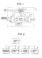
- Fig. 1 is a circuit block diagram illustrating an embodiment of a character pattern converting circuit according to the present invention;
- Fig. 2 is a block diagram illustrating a character output device with use of the embodiment of Fig. 1;
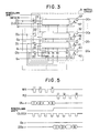
- Fig. 3 is a circuit block diagram of a matrix circuit for use in the embodiment of Fig. 1;
- Fig. 4 is a view exemplarily illustrating the conversion of a character pattern according to the present embodiment of Fig. 1;
- Fig. 5 is a time chart illustrating the operation of the matrix circuit when effecting vertical/lateral conversion in conformity with the embodiment of Fig. 1; and
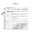
- Fig. 6 is a time chart of the matrix circuit when inclining a character pattern (converting it to italics) in conformity with the embodiment of Fig. 1.
- Now an embodiment of a character pattern converting circuit according to the present invention will be described with reference to the accompanying drawings.
- Fig. 1 is a block diagram illustrating an embodiment of a character pattern converting circuit according to the present invention, and Fig. 2 is a block diagram exemplarily illustrating a character output device constructed with use of the character pattern converting circuit.
- First, as illustrated in Fig. 2, the
control part 1 consists of a microcomputer for example and controls respective illustrated portions of the present circuit. Thecharacter generator 2 stores therein many character patterns in dot matrices, and issues character pattern data (character data) instructed by thecontrol part 1. The character pattern converting circuit 3 (hereinafter simply referred to as a converting circuit) incorporates thereinto character data from thecharacter generator 2 on the basis of the instruction from thecontrol part 1 to effect vertical/lateral conversion or inclination conversion, and delivers character data converted as such. Thebuffer memory 4 stores those converted character data in proper areas thereof instructed by thecontrol part 1. Theoutput part 5, a printing part of a printer for example, prints character data taken out from thebuffer memory 4 on the basis of an instruction from thecontrol part 1. - The converting
circuit 3 is constructed as illustrated in Fig. 1. As shown in the same figure, thematrix control part 6 consists of a counter, a register, and gates, and serves to count a write signal (hereinafter, referred to as a WR signal) issued from thecontrol part 1 for writing character data in thematrix circuit 8 while serving to count a read signal (hereinafter referred to as an RD signal) issued from thecontrol part 1 for reading character data converted in thematrix circuit 8 thereof. In addition, thematrix control part 6 includes a register for setting the presence of switching between LSB/MSB switching circuits 7 and 9 serving to symmetrically switch the order of the LSB and MSB of data bits of the concerning character data, and for setting the presence of inclination of the vertical/lateral conversion in thematrix circuit 8. This register is set by thecontrol part 1. Theswitching circuits 7 and 9 are respectively located at input and output parts of thematrix circuit 8 for symmetrically inverting the order of the LSB and MSB of data bits of the concerning character data entered in accordance with an instruction from thematrix control part 6 and delivering it, or for delivering that concerning character data as it is without inverting it. - The
matrix circuit 8 has circuit configuration illustrated for example in Fig. 3. This circuit configuration is exemplarily provided for a character pattern of 8 rows by 8 columns. 8bits shift registers 10 to 17 (corresponding to SN 74199 available from Texas Instrument Inc.) have eight-stage configuration in which parallel outputs QA to QH respectively are connected with the next stage parallel inputs A to H, whereby they form registers of 8 by 8 matrix arrangement which are capable of shifting their contents in the row direction (right direction in Fig. 3) and in the column direction thereof (upper direction in the same figure). Timing control and switching control between row and column shifts of these registers are respectively effected by a clock signal and a row/column shift signal from thematrix control part 6. The concerning character data are entered into thoseshift registers 10 to 17 in two ways, in the row and column directions: outputs at DI0 to DI7 of the LSB/MSB switching circuit 7 are entered into parallel inputs A to H of theshift register 10 when they are to be entered in the column direction, while they are entered into serial inputs J,of the
shift registers 10 to 17 via theAND gates 20 to 27 when they are to be entered in the row direction. Moreover, when the concerning character data is converted and delivered from theshift registers 10 to 17, which is the row shift, G0 to G7 controlled by thematrix control part 6 control the enabling/inhibition of the shift operations of theshift registers 10 to 17, which G0 to G7 are respectively connected to theAND gates 30 to 37 viainverters 40 to 47 and control outputs delivered from the outputs QH of theshift registers 10 to 17. Outputs at DO0 to DO7 of theAND gates 30 to 37 are delivered to the LSB/MSB switching circuit 9. - In succession, operation of the present embodiment will be described.
- First, the vertical/lateral conversion will be described, in which a character pattern in Fig. 4 (a) is rotated by +90° as shown in the same figure (b). As illustrated in Figs. 1 to 3, the
control part 1 sets, for the vertical/lateral conversion by +90°, the registers in thematrix control part 6, and issues a row/column shift signal which requires for an input of the concerning character data into theshift registers 10 to 17 to be arranged in the column direction. In addition, thecontrol part 1 thereupon sets the LSB/MSB switching circuits 7 and 9 respectively to states with and without switching. Then, thecontrol part 1 takes out first row data Da1 to Dh1 (ath row, first column data is assumed to be Da1) of a character pattern, shown in Fig. 4 (a) for example, in thecharacter generator 2, and writes them into the convertingcircuit 3. Thematrix control part 6 receives a WR signal from thecontrol part 1 to issue a clock pulse to the shift registers 10 to 17 as shown in the time chart of Fig. 5, whereby the above-described data Da1 to Dh1 passing without switching through the LSB/MSB switching circuit 7 are respectivley stored in theshift register 10 through the inputs H to A thereof. Second column data Da2 to Dh2 of the character pattern are also rendered to the same processing, and they are respectively stored in theshift register 10 through the inputs H to A thereof while the data Da1 to Dh1 are shifted to the shift register 11, on the basis of the second clock pulse shown in Fig. 5 The character patterns are successively entered up to the eight column data Da8 to Dh8 by the same processing, whereby the character data are shifted in order in the column direction through the shift registers 10 to 17 and stored therein. Thematrix control part 6, after counting the WR signal to 8 pulses, switches the row/column signal from the column shift to the row shift as shown in Fig. 5. In succession, thematrix control part 6 issues a clock pulse to the shift registers 10 to 17 on the basis of the RD signal from thecontrol part 1. Based upon this timing, data in the shift registers 10 to 17 are shifted in the row direction, whereby Da1 to Da8 are delivered from the respective QH outputs of the shift registers 10 to 17 via ANDgates 30 to 37. These data Da1 to Da8 are switched in their bit order of the LSB and MSB through the LSB/MSB switching circuit 9, delivered, and stored in thebuffer memory 4 under the control of thecontrol part 1. These are first column data shown in Fig. 4(b). In succession, with the same processing effected on the basis of the next RD signal, the contents of the shift registers 10 to 17 are further shifted in the row direction, whereby Db1 to Db8 are delivered respectively to the outputs of the ANDgates 30 to 37, and after being switched by the LSB/MSB switching circuit 9, stored in thebuffer memory 4. In such a manner, the character data in the shift registers 10 to 17 are shifted in order in the row direction and delivered owing to pulses of theRD signal 8, and after being switched by the LSB/MSB switching circuit 9, stored in thebuffer memory 4 as shown in Fig. 4 (b). - As described above, any character data is written into the shift registers 10 to 17 in the column direction and read from the row direction thereof, and thereafter switched in their order of the LSB and MSB, whereby the character pattern shown in Fig. 4 (a) is rendered to +90° vertical/lateral conversion as shown in the same figure (b). The
control part 1 transmits the contents of thebuffer memory 4 to theoutput part 5. - Moreover, when the character pattern as illustrated in Fig. 4 (a) is rendered to -90° rotation vertical/lateral conversion as shown in the same figure (c), with the LSB/
MSB switching circuits 7 and 9 being set respectively to states with switching and without switching, quite the same processing as in +90° may be effected. - Successively, inclination processing (conversion to Italics), a case for example of converting the character pattern of Fig. 4 (a) to that of the same figure (d) will be described. First, in the same manner as described above, the
control part 1 sets, for effecting the inclination prccessing, the registers in thematrix control part 6, and sets the concerning character data such that they are entered into the shift registers 10 to 17 in the row direction, and furthermore sets both the LSB/MSB switching circuits 7 and 9 to their states without switching. In succession, thecontrol part 1 writes the first column data Da1 to Dh1 of the character pattern of Fig. 4 (a) into the convertingcircuit 3 as described previously. Thematrix control part 6 receives that WR signal to issue a clock pulse to the shift registers 10 to 17 as illustrated in the time chart of Fig. 6, whereby the data Da1 to Dh1 are entered into the shift registers 17 to 10 through the J andinputs thereof via the LSB/
MSB switching circuit 7 and the ANDgates 20 to 27 and respectively stored therein. With the character pattern rendered in succession to the same processing in such a manner up to the eight column data Da8 to Dh8 thereof, the character data are shifted in order through the shift registers 10 to 17 and stored therein, and finally all the data of the character pattern are stored therein. Thematrix control part 6, after counting the WR signal by eight pulses, switches a DATA IN signal as illustrated in Fig. 6 to set all outputs of the ANDgates 20 to 27 to "L". In succession, thematrix control part 6 issues a clock pulse to the shift registers 10 to 17 on the basis of the RD signal from thecontrol part 1, while at the same time the shift registers 12 to 17 are inhibited in their operation owing to G2 to 7 and only the shift registers 10, 11 are shifted as shown in Fig. 6. Simultaneously, those signals on G2 to 8 are entered into the ANDgates 32 to 37 via theinverters 42 to 47, whereby "L" is provided to DO2 to DO7 while the data Dh1 and Dg1 of Fig. 4 (a) are provided only to DO0 and DO1. Those latter data are delivered via the LSB/MSB switching circuit 9 and stored in thebuffer memory 4 with the aid of thecontrol part 1. - These stored data are first column data shown in Fig. 4 (d). In succession, the same processing is effected by the second RD signal, and since the shift registers 14 to 17 are inhibited in their shift operation by G4 to 7, contents of only the shift registers 10 to 13 are shifted. Therefore, only DO0 to DO3 respectively provide outputs Dh2, Dg2, Df1, and De1, and the remaining Do4 to Do7 provide "L". In the same manner, with the third RD signal, since the shift registers 16 and 17 are inhibited in their shift operation owing to G6 and 7, DO0 to DO5 respectively provide Dh3, Dg3, Df2, De2, Dd1, and Dc1, and the remaining DO6 and DO7 provide "L". With the fourth shift RD signal, all inhibitions of the concerning shift operation due to G0 to G7 are released, and all the shift registers, while keeping the contents thereof shifted in order, are shifted in the row direction at each clock pulse. Since the DATA IN signal is "L" when the RD signal is issued, all the outputs of the AND
gates 20 to 27 also become "L", and hence "L" is entered in order in the shift registers which are empty as a result of those shift registers being shifted, whereby the shift register which delivers all 8 bit data provides "L" by a clock pulse thereafter. - Effecting in such a manner the same processing based on Fig. 6, the character pattern of Fig. 4 (a) is converted as shown in the same figure (d) with eleven times of the RD signal. As described above, each row shift operation of the shift registers is inhibited in order by the signals on the terminals G0 to G7, whereby character data to be delivered are shifted in order to enable the character to be inclined.
- Although the above description was for a case of the character pattern inclined to the right as shown in Fig. 4 (d), for a case thereof inclined to the left the same processing may be conducted while setting both the LSB/
MSB switching circuits 7 and 9 to a state with switching or timings on the G0 to G7 may be reversed in their order. - In addition, although the above description was for a case of the character pattern wherein it is shifted for its inclination two bits at a time from the lower rank of the bits as shown in Fig. 4 (d), provided the timing of releasing the inhibition of the shift operations of G0 to G7 in Fig. 6 is shifted in order one at a time at each RD signal, inclination for each bit is also assured. Provided the degree of such timing of shifting G0 to G7 is arbitrarily changed, the degree and fineness of inclination of a character pattern can be controlled.
- Moreover, a combination of the vertical/lateral conversion and the processing of inclination described above for converting any character pattern to that as illustrated in Fig. 4 (e) is also possible. In this case, when any character is entered into the shift registers 10 to 17, it may be effected with column shift as in the vertical/lateral conversion, and when the character data is delivered, the respective shift registers may be inhibited in their shift operation by G0 to G7 and delivered while permitting the contents thereof to be shifted in order, in the same manner as in the inclination processing. In case of Fig. 4 (a), the LSB/
MSB switching circuits 7 and 9 are previously set respectively to their states without switching and with switching. - Furthermore, although in the above description a character pattern of 8 rows by 8 columns was disclosed, another character patterns of arbitrary sizes may also be possible.
- According to the present invention, as described above, the character pattern converting circuit is adapted to include a matrix circuit having shift registers arranged in the form of a matrix which processes a character pattern issued from the character generator to enter in order thereinto the character pattern in the row or column direction and deliver it in the row direction, and to thereupon shift respective bits constituting the character pattern simultaneously or successively; the LSB/MSB switching circuits positioned at input and output portions of the matrix circuit for switching the order of the LSB and MSB of the respective bits; and a matrix control part for controlling the write and read of the character pattern into and from the matrix circuit. Accordingly, the character pattern converting circuit can process at a high speed the vertical/lateral conversion of +90° and -90° rotations, and right and left inclination processings.
- Although a certain preferred embodiments have been shown and described, it should be understood that many changes and modifications may be made therein without departing from the scope of the appended claims.
Claims (3)
Applications Claiming Priority (2)
| Application Number | Priority Date | Filing Date | Title |
|---|---|---|---|
| JP61123788A JPS62280043A (en) | 1986-05-30 | 1986-05-30 | Character pattern conversion circuit |
| JP123788/86 | 1986-05-30 |
Publications (3)
| Publication Number | Publication Date |
|---|---|
| EP0247622A2 true EP0247622A2 (en) | 1987-12-02 |
| EP0247622A3 EP0247622A3 (en) | 1990-04-04 |
| EP0247622B1 EP0247622B1 (en) | 1992-11-11 |
Family
ID=14869312
Family Applications (1)
| Application Number | Title | Priority Date | Filing Date |
|---|---|---|---|
| EP87107820A Expired EP0247622B1 (en) | 1986-05-30 | 1987-05-29 | Character pattern converting circuit |
Country Status (4)
| Country | Link |
|---|---|
| US (1) | US4808985A (en) |
| EP (1) | EP0247622B1 (en) |
| JP (1) | JPS62280043A (en) |
| DE (1) | DE3782540T2 (en) |
Cited By (5)
| Publication number | Priority date | Publication date | Assignee | Title |
|---|---|---|---|---|
| FR2633753A1 (en) * | 1988-05-10 | 1990-01-05 | Canon Kk | PRINTING APPARATUS |
| EP0424885A2 (en) * | 1989-10-24 | 1991-05-02 | Oki Electric Industry Co., Ltd. | Control apparatus of high speed/high quality printer |
| EP0435575A2 (en) * | 1989-12-27 | 1991-07-03 | Xerox Corporation | Method for slanting a generic font format while inserting corrective pixels to improve print quality |
| GB2243009A (en) * | 1990-04-09 | 1991-10-16 | Samsung Electronics Co Ltd | Aligning print data for a serial printer |
| DE4224955A1 (en) * | 1992-07-24 | 1994-01-27 | Francotyp Postalia Gmbh | Process and arrangement for internal cost center printing |
Families Citing this family (11)
| Publication number | Priority date | Publication date | Assignee | Title |
|---|---|---|---|---|
| JPS6370381A (en) * | 1986-09-12 | 1988-03-30 | インターナショナル・ビジネス・マシーンズ・コーポレーション | Rotation of image data |
| US5175811A (en) * | 1987-05-20 | 1992-12-29 | Hitachi, Ltd. | Font data processor using addresses calculated on the basis of access parameters |
| JPH0747326B2 (en) * | 1987-07-21 | 1995-05-24 | 富士通株式会社 | Character pattern converter |
| JPH01225988A (en) * | 1988-03-07 | 1989-09-08 | Iiguretsuku Syst:Kk | Information processing circuit chip |
| JP2748004B2 (en) * | 1988-05-18 | 1998-05-06 | 京セラ株式会社 | Rotation processing method of character pattern group |
| JP2748003B2 (en) * | 1988-05-18 | 1998-05-06 | 京セラ株式会社 | Character pattern rotation processing method |
| US5079739A (en) * | 1988-09-23 | 1992-01-07 | Datacard Corporation | Apparatus and method for converting bit-mapped data from row orientation to column or orientation |
| JPH04500784A (en) * | 1988-09-23 | 1992-02-13 | データカード コーポレイション | ROM conversion device and method |
| US5150108A (en) * | 1989-12-27 | 1992-09-22 | Xerox Corporation | Method for slanting a generic font format while inserting corrective pixels to improve print quality |
| US5325108A (en) * | 1990-03-02 | 1994-06-28 | Unisplay S.A. | Information displays |
| JP3375764B2 (en) * | 1994-12-26 | 2003-02-10 | 三菱電機株式会社 | Font generator |
Citations (4)
| Publication number | Priority date | Publication date | Assignee | Title |
|---|---|---|---|---|
| FR2254190A5 (en) * | 1973-12-07 | 1975-07-04 | Logabax | |
| JPS5510647A (en) * | 1978-07-10 | 1980-01-25 | Toshiba Corp | Longitudinal and lateral conversion system for pattern |
| JPS5543676A (en) * | 1978-09-22 | 1980-03-27 | Fujitsu Ltd | Vertical-horizontal conversion system |
| EP0159461A2 (en) * | 1984-04-27 | 1985-10-30 | International Business Machines Corporation | Image processing system |
Family Cites Families (4)
| Publication number | Priority date | Publication date | Assignee | Title |
|---|---|---|---|---|
| JPS5087244A (en) * | 1973-12-05 | 1975-07-14 | ||
| FR2443335A1 (en) * | 1978-12-06 | 1980-07-04 | Cii Honeywell Bull | RECORDING CONTROL DEVICE FOR POINT RECORDING MACHINE |
| JPS57136687A (en) * | 1981-02-19 | 1982-08-23 | Ricoh Kk | Output converter for character generator |
| JPS58159184A (en) * | 1982-03-17 | 1983-09-21 | Nec Corp | Picture turning device |
-
1986
- 1986-05-30 JP JP61123788A patent/JPS62280043A/en active Granted
-
1987
- 1987-05-18 US US07/050,477 patent/US4808985A/en not_active Expired - Lifetime
- 1987-05-29 DE DE8787107820T patent/DE3782540T2/en not_active Expired - Lifetime
- 1987-05-29 EP EP87107820A patent/EP0247622B1/en not_active Expired
Patent Citations (4)
| Publication number | Priority date | Publication date | Assignee | Title |
|---|---|---|---|---|
| FR2254190A5 (en) * | 1973-12-07 | 1975-07-04 | Logabax | |
| JPS5510647A (en) * | 1978-07-10 | 1980-01-25 | Toshiba Corp | Longitudinal and lateral conversion system for pattern |
| JPS5543676A (en) * | 1978-09-22 | 1980-03-27 | Fujitsu Ltd | Vertical-horizontal conversion system |
| EP0159461A2 (en) * | 1984-04-27 | 1985-10-30 | International Business Machines Corporation | Image processing system |
Non-Patent Citations (4)
| Title |
|---|
| IBM TECHNICAL DISCLOSURE BULLETIN, vol. 17, no. 10, March 1975, pages 3026-3028, New York, US; D.E. GOLD: "Shift register implemented image rotator/transposer" * |
| IBM TECHNICAL DISCLOSURE BULLETIN, vol. 18, no. 10, March 1976, pages 3390-3391, New York, US; D.A. CUMMINS et al.: "Generating slanted characters on a scanned display" * |
| PATENT ABSTRACTS OF JAPAN, vol. 4, no. 39 (P-4)[521], 28th March 1980, page 52 P 4; & JP-A-55 010 647 (TOKYO SHIBAURA DENKI K.K.) 25-01-1980 * |
| PATENT ABSTRACTS OF JAPAN, vol. 4, no. 78 (P-14)[560], 6th June 1980, page 122 P 14; & JP-A-55 043 676 (FUJITSU K.K.) 27-03-1980 * |
Cited By (10)
| Publication number | Priority date | Publication date | Assignee | Title |
|---|---|---|---|---|
| FR2633753A1 (en) * | 1988-05-10 | 1990-01-05 | Canon Kk | PRINTING APPARATUS |
| EP0424885A2 (en) * | 1989-10-24 | 1991-05-02 | Oki Electric Industry Co., Ltd. | Control apparatus of high speed/high quality printer |
| EP0424885A3 (en) * | 1989-10-24 | 1992-10-21 | Oki Electric Industry Co., Ltd. | Control apparatus of high speed/high quality printer |
| EP0435575A2 (en) * | 1989-12-27 | 1991-07-03 | Xerox Corporation | Method for slanting a generic font format while inserting corrective pixels to improve print quality |
| EP0435575A3 (en) * | 1989-12-27 | 1991-09-18 | Xerox Corporation | Method for slanting a generic font format while inserting corrective pixels to improve print quality |
| GB2243009A (en) * | 1990-04-09 | 1991-10-16 | Samsung Electronics Co Ltd | Aligning print data for a serial printer |
| GB2243009B (en) * | 1990-04-09 | 1994-01-26 | Samsung Electronics Co Ltd | Aligning print data for a serial printer |
| DE4224955A1 (en) * | 1992-07-24 | 1994-01-27 | Francotyp Postalia Gmbh | Process and arrangement for internal cost center printing |
| US5790768A (en) * | 1992-07-24 | 1998-08-04 | Francotyp-Postalia Ag & Co. | Process and configuration for an internal cost accounting printout |
| DE4224955C2 (en) * | 1992-07-24 | 1998-11-26 | Francotyp Postalia Gmbh | Arrangement and procedure for internal cost center printing |
Also Published As
| Publication number | Publication date |
|---|---|
| EP0247622A3 (en) | 1990-04-04 |
| DE3782540T2 (en) | 1993-06-03 |
| DE3782540D1 (en) | 1992-12-17 |
| US4808985A (en) | 1989-02-28 |
| JPS62280043A (en) | 1987-12-04 |
| JPH0560425B2 (en) | 1993-09-02 |
| EP0247622B1 (en) | 1992-11-11 |
Similar Documents
| Publication | Publication Date | Title |
|---|---|---|
| US4808985A (en) | Character pattern converting circuit | |
| CA1040254A (en) | Dot matrix printer with slanted print head and modular skewing of dot pattern information | |
| US5012434A (en) | Apparatus and method for selective rotation of data printed by a matrix printer | |
| EP0137147B1 (en) | Pattern processing system | |
| US4400791A (en) | Dot matrix printer with compressed character data storage | |
| GB2066527A (en) | Information processor with facilities for correcting data in a data store | |
| US5117468A (en) | Image processing system capable of carrying out local processing for image at high speed | |
| US4071909A (en) | Digital interface system for a printer | |
| US4935897A (en) | Semiconductor memory device suitable for use as a dot image buffer for a printer | |
| JPS6133711B2 (en) | ||
| EP0581515B1 (en) | Dot generator for matrix print head | |
| GB2091467A (en) | Electronic equipment | |
| JPS5913642Y2 (en) | dot matrix display device | |
| EP0190619A2 (en) | Dot character display apparatus | |
| KR890001867B1 (en) | Latter image modulating method and device | |
| JPH023513B2 (en) | ||
| SU849195A1 (en) | Device for converting data to video signal | |
| JPH0226234B2 (en) | ||
| JPS61248756A (en) | Fringing pattern forming apparatus of printing machine | |
| JPS61215583A (en) | Character pattern rotation system | |
| JPS59208681A (en) | Printer | |
| JPS6061982A (en) | Magnetic bubble memory | |
| JPS6137441A (en) | High-speed printing processing system of dot printer | |
| JPS62255155A (en) | Printing control circuit of dot matrix printer | |
| JPS6321210B2 (en) |
Legal Events
| Date | Code | Title | Description |
|---|---|---|---|
| PUAI | Public reference made under article 153(3) epc to a published international application that has entered the european phase |
Free format text: ORIGINAL CODE: 0009012 |
|
| AK | Designated contracting states |
Kind code of ref document: A2 Designated state(s): DE FR GB |
|
| PUAL | Search report despatched |
Free format text: ORIGINAL CODE: 0009013 |
|
| RHK1 | Main classification (correction) |
Ipc: G06K 15/02 |
|
| AK | Designated contracting states |
Kind code of ref document: A3 Designated state(s): DE FR GB |
|
| 17P | Request for examination filed |
Effective date: 19900725 |
|
| 17Q | First examination report despatched |
Effective date: 19910723 |
|
| GRAA | (expected) grant |
Free format text: ORIGINAL CODE: 0009210 |
|
| AK | Designated contracting states |
Kind code of ref document: B1 Designated state(s): DE FR GB |
|
| REF | Corresponds to: |
Ref document number: 3782540 Country of ref document: DE Date of ref document: 19921217 |
|
| ET | Fr: translation filed | ||
| PLBE | No opposition filed within time limit |
Free format text: ORIGINAL CODE: 0009261 |
|
| STAA | Information on the status of an ep patent application or granted ep patent |
Free format text: STATUS: NO OPPOSITION FILED WITHIN TIME LIMIT |
|
| 26N | No opposition filed | ||
| REG | Reference to a national code |
Ref country code: GB Ref legal event code: IF02 |
|
| PGFP | Annual fee paid to national office [announced via postgrant information from national office to epo] |
Ref country code: FR Payment date: 20060515 Year of fee payment: 20 |
|
| PGFP | Annual fee paid to national office [announced via postgrant information from national office to epo] |
Ref country code: GB Payment date: 20060524 Year of fee payment: 20 |
|
| PGFP | Annual fee paid to national office [announced via postgrant information from national office to epo] |
Ref country code: DE Payment date: 20060525 Year of fee payment: 20 |
|
| REG | Reference to a national code |
Ref country code: GB Ref legal event code: PE20 |
|
| PG25 | Lapsed in a contracting state [announced via postgrant information from national office to epo] |
Ref country code: GB Free format text: LAPSE BECAUSE OF EXPIRATION OF PROTECTION Effective date: 20070528 |