EP0257911A2 - Memory pointer with clustering - Google Patents
Memory pointer with clustering Download PDFInfo
- Publication number
- EP0257911A2 EP0257911A2 EP87307102A EP87307102A EP0257911A2 EP 0257911 A2 EP0257911 A2 EP 0257911A2 EP 87307102 A EP87307102 A EP 87307102A EP 87307102 A EP87307102 A EP 87307102A EP 0257911 A2 EP0257911 A2 EP 0257911A2
- Authority
- EP
- European Patent Office
- Prior art keywords
- memory
- data
- addresses
- counter
- event
- Prior art date
- Legal status (The legal status is an assumption and is not a legal conclusion. Google has not performed a legal analysis and makes no representation as to the accuracy of the status listed.)
- Withdrawn
Links
Images


Classifications
-
- G—PHYSICS
- G06—COMPUTING; CALCULATING OR COUNTING
- G06F—ELECTRIC DIGITAL DATA PROCESSING
- G06F11/00—Error detection; Error correction; Monitoring
- G06F11/22—Detection or location of defective computer hardware by testing during standby operation or during idle time, e.g. start-up testing
- G06F11/25—Testing of logic operation, e.g. by logic analysers
-
- G—PHYSICS
- G01—MEASURING; TESTING
- G01R—MEASURING ELECTRIC VARIABLES; MEASURING MAGNETIC VARIABLES
- G01R31/00—Arrangements for testing electric properties; Arrangements for locating electric faults; Arrangements for electrical testing characterised by what is being tested not provided for elsewhere
- G01R31/28—Testing of electronic circuits, e.g. by signal tracer
- G01R31/317—Testing of digital circuits
- G01R31/3177—Testing of logic operation, e.g. by logic analysers
-
- G—PHYSICS
- G06—COMPUTING; CALCULATING OR COUNTING
- G06F—ELECTRIC DIGITAL DATA PROCESSING
- G06F11/00—Error detection; Error correction; Monitoring
- G06F11/30—Monitoring
- G06F11/34—Recording or statistical evaluation of computer activity, e.g. of down time, of input/output operation ; Recording or statistical evaluation of user activity, e.g. usability assessment
- G06F11/3466—Performance evaluation by tracing or monitoring
- G06F11/348—Circuit details, i.e. tracer hardware
Definitions
- This invention relates to data acquisition systems. More particularly, this invention relates to a memory pointer for such a system for acquiring data occurring before and after an event of interest, known as "clustering" of data around an event.
- An event is one of a number of specified combinations of signals, such as an instruction generated by logic within a circuit under test.
- Logic analyzers are commonly used today to analyze the digital signals generated within a circuit.
- a logic analyzer performs a number of functions, including acquiring and storing signals generated by logic within the circuit under test.
- One particular use of an analyzer is to monitor the instructions of a microprocessor within a circuit and data generated therewith to determine if the circuit is operating as desired.
- the analyzer acts as a data acquisition system to acquire and store in memory data "clustered" around an event, i.e., data occurring before and after the event.
- the data is first continuously acquired and stored until an event occurs.
- the continuous storage of new data will cause the memory to "roll over” if no event occurs and is stored before the memory reaches its maximum address.
- Once it rolls over data is written over previously acquired data until an event terminates the acquisition.
- the event itself is then stored in memory and data occurring after the event is acquired and stored until the memory reaches its maximum address. The event is therefore stored at an intermediate memory address with data clustered around it at adjacent addresses.
- the primary drawback of conventional data acquisition systems is the limited clustering available. Only data clustered around a single event can be permanently stored, regardless of the acquisition memory size. To store data surrounding several events, the acquisition system must be continuously reset after each acquisition. Data can be lost if several events of interest occur so rapidly in sequence that the acquisition memory cannot be cleared fast enough to accept new data.
- a second drawback of this conventional data acquisition systems is the unbalanced acquisition of data clustered around an event.
- the event may be stored at any intermediate memory address, close to or far from a memory boundary.
- Several data samples may be stored before the event and many more than are useful stored afterward.
- the problem is compounded because the after-acquired data may be written over previously acquired data of substantial value.
- a data acquisition system that overcomes these drawbacks should provide for multiple clustering of events and data within an acquisition memory so that a number of events and their data can be acquired and permanently stored.
- the system should also provide as much as possible for a balanced acquisition of data before and after each event. A balance ensures that sufficient data is acquired for analysis of the test circuit's operation.
- An object of the invention is to provide an improved data acquisition system for acquiring data clustered around an event of interest, the event being defined as specified combination of input signals.
- a second object of the invention is to provide for multiple clustering of data and events within a limited acquisition memory.
- a third object of the invention is to balance the acquisition of data around each of the several events acquired and permanently stored in memory.
- a fourth object of the invention is to implement a memory pointer for generating addresses for data and events within a data acquisition system using commercially available logic circuits to generate the memory addresses.
- a memory pointer comprises means for generating memory addresses and a means for controlling the address generating means.
- the control means directs the address generating means to generate a repeating series of addresses to store data samples.
- the repeating series causes data to overwrite previously acquired data at those addresses until a specified event occurs and is stored in memory.
- the address generating means is then directed to generate a following series of addresses to store data after each specified event is stored.
- the control means directs the address generating means to generate another repeating series of addresses before and another following series of addresses after each specified event.
- the address generating means in this embodiment may include a plurality of digital counters, with a first counter generating lower order address bits and a second counter generating higher order address bits.
- the control means may include a programmable logic array configured to control the digital counters to generate the repeating sequence before and the following sequence after each specified event.
- Fig. 1 shows a block diagram of a portion of the data acquisition system 10 that includes a memory pointer circuit 12 embodying the invention.
- the system itself may contain a number of elements, but only those elements necessary to understand the function of the memory pointer 12 are shown and discussed herein.
- Target information from the circuit or device to be analyzed is carried to the system 10 through an acquisition bus 13.
- the information includes addresses, data, and control signals.
- the information is stored or latched by digital latches 14 because the information is valid on the bus 13 for only a brief period.
- the latches 14, as well as other elements in the system 10, are clocked by a system clock 16.
- Word recognizer logic 18 provides combinational event recognition of the information, and a state machine 22 provides sequential event recognition. The type of event recognition desired is selected by the operator via selection logic 24. These elements are controlled in a conventional manner by a microprocessor 26, with the connection to the elements omitted for clarity. When an event (sequential or combinatorial) is recognized, an event signal appears at the output of the state machine 22 on an event bus 28 that routes the signal to the memory pointer 12.
- the memory pointer 12 generates memory addresses for an acquisition memory 34 to store in the memory recognized events and related data occuring before and after each event.
- the events and data are routed from the latches 14 on each clock signal not only to the word recognizer 18 but also directly to the acquisition memory 34. There they are stored at the addresses provided by the memory pointer 12 through an address bus 36.
- These addresses are generated in one of two modes of pointer operation: regular and cluster. In the regular mode, the pointer 12 stores data at an address and then checks to determine if the stored data is a recognized event. If the data is not recognized event, a new address is not generated. The current memory address does not change, and the next data from the latches 14 is written over the previously stored data at the same address. If the data is a recognized event, the memory address is incremented and the next data is stored at a new address. Only recognized events are therefore stored in the acquisition memory 34 with the pointer 12 in the regular mode.
- the memory pointer 12 In the clustering mode, however, clusters of data and events are stored in the acquisition memory 34.
- the memory pointer 12 first generates a repeating sequence of addresses to store data each clock cycle in memory 34 in a "circular" buffer. Data continues to be written over previously acquired data in this buffer as these addresses repeat. Once an event is stored and recognized, the memory pointer moves to a new location in memory.
- the pointer 12 then generates a following sequence of addresses once to store data in memory 34 in a straight buffer. After completing the above-mentioned following sequence, the pointer 12 generates another repeating sequence of addresses to store data for the next event.
- the mode therefore allows for multiple clustering of data around events in a single acquisition memory.
- the stored data and events can be read by the microprocessor 26 via an address bus 38 and data bus 40 and can be displayed on a screen for analysis.
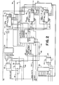
- the hardware comprising the memory pointer 12 is shown in Fig. 2 and is listed in Table 1 below. This embodiment of the invention, of course, is shown only for purposes of illustration and is not intended to limit the scope of the invention.
- the counters 42, 44, 46 generate the memory addresses for the acquisition memory 34.
- Counter 42 provides the lower portion of the address, and counters 44 and 46 provide the upper portion, the address bits linked together on the address bus 36.
- the operation of the counters is controlled by a programmable logic array (PLA) 48 as described herein.
- PLA programmable logic array
- Counter 42 generates a repeating sequence of memory addresses that "rolls over” each time the counter counts past its maximum number, fifteen, to begin another count cycle.
- the counter receives a counter clock signal (CCK) at its counter clock input from AND-OR-INVERT gate 52 through an inverter 53.
- CCK counter clock signal
- RCO ripple carry output
- PLA 48 enables and disables the counter 42 and can synchronously clear its count to zero.
- Counters 44 and 46 also receive the CCK signal from gate 52 and are enabled and disabled by PLA 48. Counter 46 is further qualified by the clock carrying output (CCO) signal of counter 44. This signal is used to cascade these two counters together, so that counter 46 increments each time counter 44 completes a count cycle and will roll over on the next clock signal. Both the CCO signals of counters 44 and 46 are also fed back to the PLA 48 to alert it when either counter is about to roll over.
- CCO clock carrying output
- the source of the CCK signal of gate 52 depends on the operating mode selected. In the cluster mode, the CCK signal is provided by the system clock 16. As the clock 16 clocks data into latches 14 for the memory 34, it also clocks the counters 42, 44, 46 to generate an address for that data. In the regular mode, the CCK signal is provided by the event bus 28. Each time an event is recognized, the event signal on the bus 28 clocks the counters 42, 44, 46 to generate an address for the event.
- the operating mode is selected by command to the microprocessor 26 which controls the pointer 12 via a programming bus 54.
- the bus 54 includes a register/cluster signal that is routed to gate 52. There the signal is combined with the event signal and system clock signal at one AND input and is inverted by inverter 55 and combined with the system clock signal at a second AND input.
- the event signal itself is latched from the event bus 28 by a flip-flop 56 that routes the signal to gate 52.
- the system clock signal is routed through a delay line circuit 58 before reaching gate 52 to match the delay of the event signal through flip-flop 56.
- the P;.A 48 is kept apprised at its inputs of the state of the counters 42, 44, and 46, the operation mode chosen, and the arrival of system clock and event signals.
- the PLA 48 also receives two additional signals: a cycle/no cycle (C/NC) signal on programming bus 54 and an acquisition memory full (AF) signal from a RAM 62.
- C/NC cycle/no cycle
- AF acquisition memory full
- the AF signal alerts the PLA that the acquisition memory 34 is full and that further storage of data will overwrite previously stored data.
- the C/NC signal tells the PLA 48 whether to "cycle" and override previously clustered data when the acquisition memory is full.
- the RAM 62 is used to determine if the acquisition memory 34 is full.
- the microprocessor 26 writes a logic 1 into RAM at the first address generated by the counters 42, 44, and 46, the logic signal routed to RAM via a branch 63 of the address bus 36.
- the remainder of RAM 62 contains logic 0.
- the AF signal will therefore be a logic 0 until the acquisition memory cycles around to the first generated address, at which address the AF signal becomes a logic 1.
- the PLA 48 reads this signal if C/NC is a logic 0, calling for a "no cycle" and terminating acquisition once memory 34 is full. If, on the other hand, the C/NC signal is "cycle," the PLA 48 ignores the AF signal and will direct the counters to generate new addresses to overwrite the previously acquired data.
- the pointer 12 also includes a number of elements for matching signal propagation delays through the circuit.
- the delay line 58 in addition to matching the delay of the event signal through flip-flop 56 also delays along with inverters 68 and 70 the propagation of the clock signal to the PLA 48. This delay enables the input signals from the counters 42, 44, and 46 to be present and stable before the PLA is clocked by the system clock to read those inputs.
- Other input signals to the pointer 12 include a reset and a program enable.
- the reset signal is generated on power-up or hardware reset to set the PLA 48 and counters 42, 44, 46 to an initial memory address of zero.
- the program enable signal forces the counters into a high impedance state to allow the microprocessor 26 to place an address on bus 36 to the memory 34 and read the acquisition memory 34 via bus 40.
- the operation of the memory pointer 12 is controlled by PLA 48, whose inputs and outputs are shown in Fig. 3.
- the signals thereon are active in the logic state shown parenthetically after the signal name.
- the output signal lower-counter-clear (LCTRCL) is active when its logic state is low.
- the other output signals are EVENT, which signals occurrence of an event, and CBUF, which indicates the data stored is in a circular buffer.
- a state diagram, output table, and memory table are shown for the PLA 48 with the pointer 12 in the cluster mode.
- the clock 16 provides the counter clock signal to the counters 42, 44, and 46 in this mode, as well as the clock signal for the rest of the pointer 12 in either mode.
- the PLA 48 On power up or hardware reset, the PLA 48 begins in state 1.
- Counter 42 the least significant counter, counts each clock cycle to produce a sequence of addresses that repeats each sixteen clock cycles. Counters 44 and 46 are not enabled. If no event occurs within the first run through the sequence, the RCO signal is asserted (indicating the counter is ready to roll over on the next clock cycle) and the PLA 48 moves to state 3. The sequence of addresses will at this point have stored sixteen samples of data within the acquisition memory 34, one sample each clock cycle. If, however, an event occurs and is stored before the counter 42 completes a first pass through the sequence, the PLA 48 moves to state 2. A third possibility also exists. If the event occurs and is stored when the counter generates its maximum address and RCO is asserted, the PLA 48 moves directly to state 4.
- state 3 the counter passes again through the sequence, awaiting the occurrence of an event and causing data samples to be written over the previously acquired data. If the counter again rolls over, it moves to state 5 and repeats the sequence. The counter then continues to move between states 3 and 5 until an event occurs. Once that happens, the PLA moves from either state 3 or 5 to state 4. In the process, of course, an event and fifteen data samples preceding the event have been stored in a circular buffer in memory with the event likely stored at an intermediate address in the sequence.
- state 4 the PLA enables the upper counters 44 and 46 to increment on the next system clock signal so that a new sequence of addresses is then generated by these counters in cooperation with counter 42.
- This following sequence of sixteen addresses stores data samples occurring after the event in a straight buffer in memory 34.
- the PLA remains in state 4 until the RCO signal is again asserted, indicating the completion of the following sequence.
- the PLA 48 then returns to state 1 to generate another repeating sequence of addresses. In the process, the upper counters are again incremented to provide a new sequence beyond the following sequence.
- Fig. 5 indicates when the PLA output signals are asserted to manipulate the counters in each PLA state.
- state 1 for example, the upper counters will be enabled by UCTRENB if the RCO and EVENT signals are present, moving the PLA directly to state 4. An event has occurred and a following series of addresses is to be generated. Counter 44 will then increment on the next clock signal. Counter 46 will also increment if counter 44 is rolling over and its CCO signal is asserted.
- state 2 the upper counters 44 and 46 will be enabled by UCTRENB when the RCO signal is asserted at the completion of a first pass through the repeating sequence. Again, the PLA moves to state 4.
- the upper counters will be enabled by UCTRENB and the lower counter 42 cleared by LCTRCLR when an event occurs and is stored, moving the PLA to state 4.
- the counter 42 is cleared to preserve data samples previously stored in the sequence at addresses above the event address. Otherwise this data would be overwritten by data following the event.
- the upper counters will again be enabled by UCTRENB to increment when RCO is asserted, indicating counter 42 will roll over on the next clock cycle to complete the following sequence of addresses.
- State 2 of the PLA exists to handle two special cases: where an event occurs before counter 42 has rolled over once; and where two events occur less than sixteen clock cycles (and therefore data samples) apart.
- the PLA 48 moves to state 2, stores the event, and then completes the sequence before moving to state 4.
- the PLA 48 moves from state 4 to state 2 to complete the sequence of addresses following the first event and then back to state 4 to generate a second, separate sequence of addresses following the second event.
- Fig. 6 is a memory diagram illustrating the operation of the PLA 48 in storing data samples in memory. Beginning at address 0, the PLA is in state 1 and counter 42 begins to generate the lower bits of addresses to store data samples. An event, however, occurs and is stored before the counter passes once through the sequence. The PLA in response moves to state 2 and completes the sequence of addresses to store data occurring after the event. The RCO signal of counter 42 is asserted, and the PLA moves from state 2 to state 4 to generate the following sequence of sixteen addresses by incrementing counter 44 and running counter 42 through another sequence.
- the PLA then enables the upper counters 44 and 46 to increment again on the next clock cycle and returns to state 1 to generate another repeating sequence of addresses. No event occurs this time before the RCO signal is asserted, and the PLA moves to state 3. From there, it moves between states 5 and 3 until an event occurs and is stored midway in the current sequence. The PLA then jumps the address to the next sequence to preserve pre-event data by incrementing counter 44 and clearing counter 42. The PLA is now in state 4, generating addresses to store data occurring 20 after the event.
- a second event occurs before sixteen addresses in the sequence following the first event have been generated and the PLA moves to state 2. There it completes the first following sequence and then moves back to state 4 to generate a second following sequence for the second event. Once the second following sequence is completed, the PLA returns again to state 1, incrementing the upper counters again in the process.
- the process of acquiring and storing data and events continues until the acquisition memory is full. At this point, the AF signal is asserted and the PLA determines whether it should begin a second cycle through the acquisition memory or stop until the current data is viewed. That decision is controlled by the 35 state of the C/NC signal on the programming bus 54.
- Whether the data stored in memory occurred before or after an event stored therein is determined by microprocessor 26 from the logic states of CBUF and EVENT. Referring to Figs. 1 and 2, these signals are routed to memory 34 on a data bus 72 to be stored with the data and events. With these two signals, the microprocessor 26 can identify the data stored in addresses higher than the event's address as preceding or following data and thereby determine where to begin reading the data. For example, if counter 42 has made one pass through a repeating sequence and an event occurs and is stored, then data in the higher addresses in the sequence are preceding data. Both EVENT and CBUF are in the high logic state, indicating a circular buffer in memory.
- Microprocessor 26 will begin reading at the address above the event and then "around" to the lower addresses below the event. If no CBUF signal is asserted, then the data is stored in a straight buffer in memory and the microprocessor 26 reads the data in order of increasing address.
- the event signal from the event bus 28 is the CCK signal to the counters 42, 44, and 46. Each time an event is detected, it is stored and the counters incremented. If data other than an event is detected, no new address is generated and the data is continually overwritten until an event occurs and is stored. In the end, the acquisition memory 34 is filled with events, but not with related data occurring before and after each event.
- the PLA 48 in this mode acts to cascade the counters 42, 44, and 46 together, enabling an upper counter to increment on the next CCK signal once a lower counter has reached its maximum count.
Abstract
A memory pointer circuit includes a plurality of counters and a programmable logic array for controlling the counters to generate addresses for an acquisition memory. The programmable logic array directs a lower counter to generate a repeating sequence of addresses to store data before an event occurs, each pass through the sequence causing previously written data to be overwritten until an event has occurred and is stored in memory. The programmable logic array then directs the upper counters to increment and the lower counter to generate a following sequence of addresses to store data after the event occurs. Once the following sequence is complete, the upper counters are again incremented and the repeating sequence of addresses is again generated. The procedure is repeated to store multiple clusters of data and events in the acquisition memory. Once the acquisition memory is full, the stored data and events can be saved or overwritten.
Description
- This invention relates to data acquisition systems. More particularly, this invention relates to a memory pointer for such a system for acquiring data occurring before and after an event of interest, known as "clustering" of data around an event. An event is one of a number of specified combinations of signals, such as an instruction generated by logic within a circuit under test.
- Logic analyzers are commonly used today to analyze the digital signals generated within a circuit. A logic analyzer performs a number of functions, including acquiring and storing signals generated by logic within the circuit under test. One particular use of an analyzer is to monitor the instructions of a microprocessor within a circuit and data generated therewith to determine if the circuit is operating as desired.
- In one aspect of its monitoring operation, the analyzer acts as a data acquisition system to acquire and store in memory data "clustered" around an event, i.e., data occurring before and after the event. The data is first continuously acquired and stored until an event occurs. With a limited size acquisition memory, the continuous storage of new data will cause the memory to "roll over" if no event occurs and is stored before the memory reaches its maximum address. Once it rolls over, data is written over previously acquired data until an event terminates the acquisition. The event itself is then stored in memory and data occurring after the event is acquired and stored until the memory reaches its maximum address. The event is therefore stored at an intermediate memory address with data clustered around it at adjacent addresses.
- The primary drawback of conventional data acquisition systems is the limited clustering available. Only data clustered around a single event can be permanently stored, regardless of the acquisition memory size. To store data surrounding several events, the acquisition system must be continuously reset after each acquisition. Data can be lost if several events of interest occur so rapidly in sequence that the acquisition memory cannot be cleared fast enough to accept new data.
- A second drawback of this conventional data acquisition systems is the unbalanced acquisition of data clustered around an event. The event may be stored at any intermediate memory address, close to or far from a memory boundary. Several data samples may be stored before the event and many more than are useful stored afterward. The problem is compounded because the after-acquired data may be written over previously acquired data of substantial value.
- A data acquisition system that overcomes these drawbacks should provide for multiple clustering of events and data within an acquisition memory so that a number of events and their data can be acquired and permanently stored. The system should also provide as much as possible for a balanced acquisition of data before and after each event. A balance ensures that sufficient data is acquired for analysis of the test circuit's operation.
- An object of the invention, therefore, is to provide an improved data acquisition system for acquiring data clustered around an event of interest, the event being defined as specified combination of input signals.
- A second object of the invention is to provide for multiple clustering of data and events within a limited acquisition memory.
- A third object of the invention is to balance the acquisition of data around each of the several events acquired and permanently stored in memory. A fourth object of the invention is to implement a memory pointer for generating addresses for data and events within a data acquisition system using commercially available logic circuits to generate the memory addresses.
- To achieve these objects, a memory pointer according to the invention comprises means for generating memory addresses and a means for controlling the address generating means. The control means directs the address generating means to generate a repeating series of addresses to store data samples. The repeating series causes data to overwrite previously acquired data at those addresses until a specified event occurs and is stored in memory. The address generating means is then directed to generate a following series of addresses to store data after each specified event is stored. Once the following series is completed, the control means directs the address generating means to generate another repeating series of addresses before and another following series of addresses after each specified event. By this technique, the memory can store a plurality of specified events along with related data. The address generating means in this embodiment may include a plurality of digital counters, with a first counter generating lower order address bits and a second counter generating higher order address bits.
- The control means may include a programmable logic array configured to control the digital counters to generate the repeating sequence before and the following sequence after each specified event.
- The foregoing and other objects, features, and advantages of the invention will become more apparent from the following detailed description of a preferred embodiment which proceeds with reference to the accompanying drawings.
-
- FIG. 1 is a block diagram of a portion of a data acquisition system including a memory pointer circuit according to the invention.
- FIG. 2 is a schematic diagram of the memory pointer circuit of Fig. 1.
- FIG. 3 is a schematic diagram of the input and output connections to a programmable logic array used in the memory pointer.
- FIG. 4 is a state diagram showing the states of the programmable logic array of Fig. 4 for generating the memory addresses.
- FIG. 5 is a programmable logic array output table showing the input signals in each state required to generate an output signal from the array.
- FIG. 6 is a memory diagram illustrating the generating of addresses by the memory pointer to acquire and permanently store data and events in the acquisition memory.
- Fig. 1 shows a block diagram of a portion of the
data acquisition system 10 that includes amemory pointer circuit 12 embodying the invention. The system itself may contain a number of elements, but only those elements necessary to understand the function of thememory pointer 12 are shown and discussed herein. - Target information from the circuit or device to be analyzed is carried to the
system 10 through an acquisition bus 13. The information includes addresses, data, and control signals. The information is stored or latched bydigital latches 14 because the information is valid on the bus 13 for only a brief period. Thelatches 14, as well as other elements in thesystem 10, are clocked by asystem clock 16. - After being latched, the information is "analyzed" to determine if a specific event or sequence of events has occurred. Word recognizer
logic 18 provides combinational event recognition of the information, and astate machine 22 provides sequential event recognition. The type of event recognition desired is selected by the operator viaselection logic 24. These elements are controlled in a conventional manner by amicroprocessor 26, with the connection to the elements omitted for clarity. When an event (sequential or combinatorial) is recognized, an event signal appears at the output of thestate machine 22 on anevent bus 28 that routes the signal to thememory pointer 12. - The
memory pointer 12 generates memory addresses for anacquisition memory 34 to store in the memory recognized events and related data occuring before and after each event. The events and data are routed from thelatches 14 on each clock signal not only to the word recognizer 18 but also directly to theacquisition memory 34. There they are stored at the addresses provided by thememory pointer 12 through anaddress bus 36. These addresses are generated in one of two modes of pointer operation: regular and cluster. In the regular mode, thepointer 12 stores data at an address and then checks to determine if the stored data is a recognized event. If the data is not recognized event, a new address is not generated. The current memory address does not change, and the next data from thelatches 14 is written over the previously stored data at the same address. If the data is a recognized event, the memory address is incremented and the next data is stored at a new address. Only recognized events are therefore stored in theacquisition memory 34 with thepointer 12 in the regular mode. - In the clustering mode, however, clusters of data and events are stored in the
acquisition memory 34. Thememory pointer 12 first generates a repeating sequence of addresses to store data each clock cycle inmemory 34 in a "circular" buffer. Data continues to be written over previously acquired data in this buffer as these addresses repeat. Once an event is stored and recognized, the memory pointer moves to a new location in memory. Thepointer 12 then generates a following sequence of addresses once to store data inmemory 34 in a straight buffer. After completing the above-mentioned following sequence, thepointer 12 generates another repeating sequence of addresses to store data for the next event. The mode therefore allows for multiple clustering of data around events in a single acquisition memory. - In either mode, the stored data and events can be read by the
microprocessor 26 via anaddress bus 38 anddata bus 40 and can be displayed on a screen for analysis. - The hardware comprising the
memory pointer 12 is shown in Fig. 2 and is listed in Table 1 below. This embodiment of the invention, of course, is shown only for purposes of illustration and is not intended to limit the scope of the invention.
- Referring to Fig. 2, the
counters acquisition memory 34.Counter 42 provides the lower portion of the address, and counters 44 and 46 provide the upper portion, the address bits linked together on theaddress bus 36. The operation of the counters is controlled by a programmable logic array (PLA) 48 as described herein. -
Counter 42 generates a repeating sequence of memory addresses that "rolls over" each time the counter counts past its maximum number, fifteen, to begin another count cycle. The counter receives a counter clock signal (CCK) at its counter clock input from AND-OR-INVERT gate 52 through aninverter 53. Whencounter 42 has reached its maximum count and will roll over on the next clock signal, it generates a ripple carry output (RCO) signal that is fed back to thePLA 48.PLA 48 enables and disables thecounter 42 and can synchronously clear its count to zero. -
Counters gate 52 and are enabled and disabled byPLA 48.Counter 46 is further qualified by the clock carrying output (CCO) signal ofcounter 44. This signal is used to cascade these two counters together, so that counter 46 increments eachtime counter 44 completes a count cycle and will roll over on the next clock signal. Both the CCO signals ofcounters PLA 48 to alert it when either counter is about to roll over. - The source of the CCK signal of
gate 52 depends on the operating mode selected. In the cluster mode, the CCK signal is provided by thesystem clock 16. As theclock 16 clocks data intolatches 14 for thememory 34, it also clocks thecounters event bus 28. Each time an event is recognized, the event signal on thebus 28 clocks thecounters - The operating mode is selected by command to the
microprocessor 26 which controls thepointer 12 via aprogramming bus 54. Thebus 54 includes a register/cluster signal that is routed togate 52. There the signal is combined with the event signal and system clock signal at one AND input and is inverted byinverter 55 and combined with the system clock signal at a second AND input. The event signal itself is latched from theevent bus 28 by a flip-flop 56 that routes the signal togate 52. The system clock signal is routed through adelay line circuit 58 before reachinggate 52 to match the delay of the event signal through flip-flop 56. - The P;.A 48 is kept apprised at its inputs of the state of the
counters PLA 48 also receives two additional signals: a cycle/no cycle (C/NC) signal onprogramming bus 54 and an acquisition memory full (AF) signal from aRAM 62. The AF signal alerts the PLA that theacquisition memory 34 is full and that further storage of data will overwrite previously stored data. The C/NC signal tells thePLA 48 whether to "cycle" and override previously clustered data when the acquisition memory is full. TheRAM 62 is used to determine if theacquisition memory 34 is full. Themicroprocessor 26 writes alogic 1 into RAM at the first address generated by thecounters branch 63 of theaddress bus 36. The remainder ofRAM 62 contains logic 0. Each time a new address is generated by incrementing thecounters RAM 62 is clocked bysystem clock 16 through a flip-flop 64 and read by thePLA 48 as the AF signal. The AF signal will therefore be a logic 0 until the acquisition memory cycles around to the first generated address, at which address the AF signal becomes alogic 1. ThePLA 48 reads this signal if C/NC is a logic 0, calling for a "no cycle" and terminating acquisition oncememory 34 is full. If, on the other hand, the C/NC signal is "cycle," thePLA 48 ignores the AF signal and will direct the counters to generate new addresses to overwrite the previously acquired data. - The
pointer 12 also includes a number of elements for matching signal propagation delays through the circuit. Thedelay line 58 in addition to matching the delay of the event signal through flip-flop 56 also delays along withinverters PLA 48. This delay enables the input signals from thecounters - Other input signals to the
pointer 12 include a reset and a program enable. The reset signal is generated on power-up or hardware reset to set thePLA 48 and counters 42, 44, 46 to an initial memory address of zero. The program enable signal forces the counters into a high impedance state to allow themicroprocessor 26 to place an address onbus 36 to thememory 34 and read theacquisition memory 34 viabus 40. - The operation of the
memory pointer 12 is controlled byPLA 48, whose inputs and outputs are shown in Fig. 3. The signals thereon are active in the logic state shown parenthetically after the signal name. For example, the output signal lower-counter-clear (LCTRCL) is active when its logic state is low. - Lower-counter-enable (LCTRENB) and upper-counter-enable (UCTRENB), on the other hand, are active when their logic states are high. The other output signals are EVENT, which signals occurrence of an event, and CBUF, which indicates the data stored is in a circular buffer.
- Referring to Figs. 4 through 6, a state diagram, output table, and memory table are shown for the
PLA 48 with thepointer 12 in the cluster mode. Theclock 16 provides the counter clock signal to thecounters pointer 12 in either mode. - On power up or hardware reset, the
PLA 48 begins instate 1.Counter 42, the least significant counter, counts each clock cycle to produce a sequence of addresses that repeats each sixteen clock cycles.Counters PLA 48 moves tostate 3. The sequence of addresses will at this point have stored sixteen samples of data within theacquisition memory 34, one sample each clock cycle. If, however, an event occurs and is stored before thecounter 42 completes a first pass through the sequence, thePLA 48 moves tostate 2. A third possibility also exists. If the event occurs and is stored when the counter generates its maximum address and RCO is asserted, thePLA 48 moves directly tostate 4. - In
state 3 the counter passes again through the sequence, awaiting the occurrence of an event and causing data samples to be written over the previously acquired data. If the counter again rolls over, it moves tostate 5 and repeats the sequence. The counter then continues to move betweenstates state state 4. In the process, of course, an event and fifteen data samples preceding the event have been stored in a circular buffer in memory with the event likely stored at an intermediate address in the sequence. - Recall that if
state 2 is entered, an event and fewer than fifteen data samples preceding the event have been stored inmemory 34. Thecounter 42 continues to generate addresses to complete a first pass through the sequence and store data samples occurring after the event. Once the pass is completed, the RCO signal is asserted andPLA 48 moves fromstate 2 tostate 4. - In
state 4 the PLA enables theupper counters counter 42. This following sequence of sixteen addresses stores data samples occurring after the event in a straight buffer inmemory 34. The PLA remains instate 4 until the RCO signal is again asserted, indicating the completion of the following sequence. ThePLA 48 then returns tostate 1 to generate another repeating sequence of addresses. In the process, the upper counters are again incremented to provide a new sequence beyond the following sequence. - Fig. 5 indicates when the PLA output signals are asserted to manipulate the counters in each PLA state. In
state 1, for example, the upper counters will be enabled by UCTRENB if the RCO and EVENT signals are present, moving the PLA directly tostate 4. An event has occurred and a following series of addresses is to be generated.Counter 44 will then increment on the next clock signal.Counter 46 will also increment ifcounter 44 is rolling over and its CCO signal is asserted. Instate 2, theupper counters state 4. In states 3 and 5, the upper counters will be enabled by UCTRENB and thelower counter 42 cleared by LCTRCLR when an event occurs and is stored, moving the PLA tostate 4. Thecounter 42 is cleared to preserve data samples previously stored in the sequence at addresses above the event address. Otherwise this data would be overwritten by data following the event. By incrementingcounters counter 42, the next sequence of addresses will begin at a different location. Once instate 4, the upper counters will again be enabled by UCTRENB to increment when RCO is asserted, indicating counter 42 will roll over on the next clock cycle to complete the following sequence of addresses. -
State 2 of the PLA exists to handle two special cases: where an event occurs beforecounter 42 has rolled over once; and where two events occur less than sixteen clock cycles (and therefore data samples) apart. In the first case, thePLA 48 moves tostate 2, stores the event, and then completes the sequence before moving tostate 4. In the second case, thePLA 48 moves fromstate 4 tostate 2 to complete the sequence of addresses following the first event and then back tostate 4 to generate a second, separate sequence of addresses following the second event. - Fig. 6 is a memory diagram illustrating the operation of the
PLA 48 in storing data samples in memory. Beginning at address 0, the PLA is instate 1 andcounter 42 begins to generate the lower bits of addresses to store data samples. An event, however, occurs and is stored before the counter passes once through the sequence. The PLA in response moves tostate 2 and completes the sequence of addresses to store data occurring after the event. The RCO signal ofcounter 42 is asserted, and the PLA moves fromstate 2 tostate 4 to generate the following sequence of sixteen addresses by incrementingcounter 44 and running counter 42 through another sequence. - The PLA then enables the
upper counters state 1 to generate another repeating sequence of addresses. No event occurs this time before the RCO signal is asserted, and the PLA moves tostate 3. From there, it moves betweenstates counter 44 and clearingcounter 42. The PLA is now instate 4, generating addresses to store data occurring 20 after the event. - A second event occurs before sixteen addresses in the sequence following the first event have been generated and the PLA moves to
state 2. There it completes the first following sequence and then moves back tostate 4 to generate a second following sequence for the second event. Once the second following sequence is completed, the PLA returns again tostate 1, incrementing the upper counters again in the process. - The process of acquiring and storing data and events continues until the acquisition memory is full. At this point, the AF signal is asserted and the PLA determines whether it should begin a second cycle through the acquisition memory or stop until the current data is viewed. That decision is controlled by the 35 state of the C/NC signal on the
programming bus 54. - Whether the data stored in memory occurred before or after an event stored therein is determined by
microprocessor 26 from the logic states of CBUF and EVENT. Referring to Figs. 1 and 2, these signals are routed tomemory 34 on adata bus 72 to be stored with the data and events. With these two signals, themicroprocessor 26 can identify the data stored in addresses higher than the event's address as preceding or following data and thereby determine where to begin reading the data. For example, ifcounter 42 has made one pass through a repeating sequence and an event occurs and is stored, then data in the higher addresses in the sequence are preceding data. Both EVENT and CBUF are in the high logic state, indicating a circular buffer in memory.Microprocessor 26 will begin reading at the address above the event and then "around" to the lower addresses below the event. If no CBUF signal is asserted, then the data is stored in a straight buffer in memory and themicroprocessor 26 reads the data in order of increasing address. - In the regular mode, the event signal from the
event bus 28 is the CCK signal to thecounters acquisition memory 34 is filled with events, but not with related data occurring before and after each event. - The
PLA 48 in this mode acts to cascade thecounters - Having illustrated and described the principles of the invention in a preferred embodiment, it should be apparent to those skilled in the art that the invention can be modified in arrangement and detail without departing from such principles. For one, the circuitry shown herein could be implemented in an integrated circuit by one skilled in the art. For another, the counters could be replaced with equivalent elements that generate an address pattern that is not necessarily a sequence, such as a series. I therefore claim all modifications coming within the spirit and scope of the following claims.
Claims (9)
1. In a data acquisition system, a memory pointer circuit for storing in an acquisition memory data occurring before and after specified events, the memory pointer circuit comprising:
signaling means for signaling the occurrence of a specified event;
address generating means in communication with the signaling means and the memory for generating memory addresses to store data and specified events in memory; and
control means in communication with the signaling means and the address generating means for directing the address generating means to generate a repeating series of addresses to store data in memory occurring before a specified event, the repeating addresses causing data to overwrite previously stored data in memory until a specified event is signaled and stored in memory, the control means then directing the address generating means to generate a following series of addresses to store data occurring after each specified event is stored,
the control means directing the address generating means to generate another repeating series of addresses before and another following series of addresses after each specified event is sensed to enable the memory to store a plurality of specified events along with related data.
2. The circuit of claim 1 in which the address generating means includes a plurality of digital counters, a first counter for generating a repeating sequence of lower order address bits and a second counter for generating higher order address bits, the second counter incrementing after the occurrence of a specified event and incrementing again after completion of the following series of addresses to generate a plurality of repeating and following series of addresses for memory.
3. The circuit of claim 1 in which the control means includes a programmable logic array means for generating control signals in response to a specified event to control the address generating means.
4. The circuit of claim 1 including RAM memory means for determining when the acquisition memory is full and alerting the control means that further storage of data will overwrite previously stored events and related data.
5. In a data acquisition system, a memory pointer circuit for storing in an acquisition memory data occurring before and after specified events, the memory pointer circuit comprising:
an event bus for signaling the occurrence of a specified event;
a first counter for generating the lower portion of the memory address;
second counter means for generating the upper portion of the memory address; and
a programmable logic array in communication with the event bus and the first and second counters for directing the first counter to generate a repeating series of address bits as the lower portion of the memory address to store data in the acquisition memory occurring before a specified event, each generation of address bits in the series causing the memory to overwrite previously stored data at that address until a specified event occurs and is stored in memory, the logic means then directing the second counter to increment the upper portion of the memory address and generate with the first counter a following series of addresses to store data occurring after each specified event, the logic means further directing the second counter to increment the upper portion of the memory address again after completion of the following series of addresses, the first counter then generating another repeating series of addresses as the lower portion of the memory address and generating with the second counter another series of following addresses for each specified event that is stored.
6. The memory pointer circuit of claim 5 in which the first and second counter means comprise 4-bit digital counters.
7. In a data acquisition system, a method of storing in memory data occurring before and after specified events, comprising:
generating a repeating series of memory addresses to store in memory data occurring before a specified event, each regeneration of addresses causing previously acquired data stored at those addresses in memory to be overwritten;
storing a specified event;
halting, in response to the storing of the specified event, the generation of the repeating series of memory addresses to preserve the last data stored;
generating a following series of memory addresses to store data occurring after each specified event; and
repeating the above steps at other addresses in memory to enable the memory to store a plurality of specified events and related data.
8. The method of claim 7 in which the series of addresses generated are sequences of a predetermined size generated by a counter, each sequence adjacent to the previous sequence in memory.
9. The method of claim 8 including determining when the memory is full to prevent further storage of data overwriting previously acquired data.
Applications Claiming Priority (2)
| Application Number | Priority Date | Filing Date | Title |
|---|---|---|---|
| US899854 | 1986-08-25 | ||
| US06/899,854 US4835736A (en) | 1986-08-25 | 1986-08-25 | Data acquisition system for capturing and storing clustered test data occurring before and after an event of interest |
Publications (2)
| Publication Number | Publication Date |
|---|---|
| EP0257911A2 true EP0257911A2 (en) | 1988-03-02 |
| EP0257911A3 EP0257911A3 (en) | 1989-10-25 |
Family
ID=25411653
Family Applications (1)
| Application Number | Title | Priority Date | Filing Date |
|---|---|---|---|
| EP87307102A Withdrawn EP0257911A3 (en) | 1986-08-25 | 1987-08-11 | Memory pointer with clustering |
Country Status (3)
| Country | Link |
|---|---|
| US (1) | US4835736A (en) |
| EP (1) | EP0257911A3 (en) |
| JP (1) | JPH0635993B2 (en) |
Cited By (5)
| Publication number | Priority date | Publication date | Assignee | Title |
|---|---|---|---|---|
| EP0420398A2 (en) * | 1989-09-29 | 1991-04-03 | Tektronix Inc. | Method for acquiring data in a logic analyzer |
| GB2300496A (en) * | 1995-05-01 | 1996-11-06 | Motorola Gmbh | Data processing system |
| GB2329267A (en) * | 1998-03-18 | 1999-03-17 | Patrick Bossert | Testing computer date-handling capability |
| EP1677195A2 (en) * | 1997-11-18 | 2006-07-05 | Altera Corporation | Enhanced embedded logic analyzer |
| EP2264600A3 (en) * | 1997-11-18 | 2011-06-22 | Altera Corporation | Enhanced embedded logic analyzer |
Families Citing this family (21)
| Publication number | Priority date | Publication date | Assignee | Title |
|---|---|---|---|---|
| JPH0221566U (en) * | 1988-07-28 | 1990-02-13 | ||
| US5038319A (en) * | 1989-04-24 | 1991-08-06 | Xerox Corporation | System for recording and remotely accessing operating data in a reproduction machine |
| DE4042262A1 (en) * | 1990-12-31 | 1992-07-02 | Richt Stefan | Analysing digital circuit functions using scanned values - involves writing into memory with pre-trace and/or centre trace to extend recording time |
| US5166734A (en) * | 1991-02-12 | 1992-11-24 | Spectrum Sciences B.V. | Imaging system including pre-transfer discharge |
| US5426741A (en) * | 1991-02-20 | 1995-06-20 | Digital Equipment Corporation | Bus event monitor |
| US7623754B1 (en) | 1995-02-23 | 2009-11-24 | Avid Technology, Inc. | Motion picture recording device using digital, computer-readable non-linear media |
| US6977673B1 (en) | 1995-02-23 | 2005-12-20 | Avid Technology, Inc. | Portable moving picture recording device including switching control for multiple data flow configurations |
| US7532807B2 (en) * | 1995-04-07 | 2009-05-12 | Avid Technology, Inc. | Combined editing system and digital moving picture recording system |
| US6102964A (en) * | 1996-10-28 | 2000-08-15 | Altera Corporation | Fitting for incremental compilation of electronic designs |
| US6035367A (en) * | 1997-04-04 | 2000-03-07 | Avid Technology, Inc. | Computer file system providing looped file structure for post-occurrence data collection of asynchronous events |
| US6112318A (en) * | 1997-08-11 | 2000-08-29 | Digital Equipment Corporation | Performance counters controlled by programmable logic |
| US6247147B1 (en) | 1997-10-27 | 2001-06-12 | Altera Corporation | Enhanced embedded logic analyzer |
| DE19849328A1 (en) * | 1998-10-26 | 2000-05-04 | Bosch Gmbh Robert | Control method for combustion engine in which parameter values are stored using ring memory to store value existing before occurrence of error |
| US6647479B1 (en) | 2000-01-03 | 2003-11-11 | Avid Technology, Inc. | Computer file system providing looped file structure for post-occurrence data collection of asynchronous events |
| US6754862B1 (en) | 2000-03-09 | 2004-06-22 | Altera Corporation | Gaining access to internal nodes in a PLD |
| CN100377097C (en) * | 2002-08-26 | 2008-03-26 | 联发科技股份有限公司 | Error eliminating device |
| US7036046B2 (en) * | 2002-11-14 | 2006-04-25 | Altera Corporation | PLD debugging hub |
| US7076751B1 (en) | 2003-01-24 | 2006-07-11 | Altera Corporation | Chip debugging using incremental recompilation |
| US7539900B1 (en) | 2003-07-29 | 2009-05-26 | Altera Corporation | Embedded microprocessor for integrated circuit testing and debugging |
| US7206967B1 (en) | 2004-02-09 | 2007-04-17 | Altera Corporation | Chip debugging using incremental recompilation and register insertion |
| US7461383B2 (en) * | 2006-08-21 | 2008-12-02 | International Business Machines Corporation | Method and apparatus for efficient performance monitoring of a large number of simultaneous events |
Citations (3)
| Publication number | Priority date | Publication date | Assignee | Title |
|---|---|---|---|---|
| JPS59172047A (en) * | 1983-03-22 | 1984-09-28 | Nippon Telegr & Teleph Corp <Ntt> | Processor additional device |
| US4513395A (en) * | 1983-03-25 | 1985-04-23 | Northwest Instrument Systems, Inc. | Apparatus and method for acquiring multiple groups of data signals from a synchronous logic system |
| EP0159588A2 (en) * | 1984-04-06 | 1985-10-30 | Advantest Corporation | Logic analyzer |
Family Cites Families (8)
| Publication number | Priority date | Publication date | Assignee | Title |
|---|---|---|---|---|
| US4040025A (en) * | 1976-03-31 | 1977-08-02 | Hewlett-Packard Company | Logic state analyzer |
| GB1593128A (en) * | 1977-08-29 | 1981-07-15 | Hewlett Packard Co | Logic state analyzer |
| US4373193A (en) * | 1977-08-29 | 1983-02-08 | Hewlett-Packard Company | Logic state analyzer |
| JPS5540460A (en) * | 1978-09-14 | 1980-03-21 | Fuji Xerox Co Ltd | Image transfer device |
| US4480317A (en) * | 1980-11-25 | 1984-10-30 | Hewlett-Packard Company | Logic state analyzer with graph of captured trace |
| FR2509936B1 (en) * | 1981-07-17 | 1986-12-19 | Thomson Csf | DISTURBANCE RECORDING SYSTEM |
| US4473889A (en) * | 1981-09-11 | 1984-09-25 | Leeds & Northrup Company | Remote correlation of sequence of events |
| US4660198A (en) * | 1985-04-15 | 1987-04-21 | Control Data Corporation | Data capture logic for VLSI chips |
-
1986
- 1986-08-25 US US06/899,854 patent/US4835736A/en not_active Expired - Lifetime
-
1987
- 1987-08-11 EP EP87307102A patent/EP0257911A3/en not_active Withdrawn
- 1987-08-20 JP JP62207348A patent/JPH0635993B2/en not_active Expired - Lifetime
Patent Citations (3)
| Publication number | Priority date | Publication date | Assignee | Title |
|---|---|---|---|---|
| JPS59172047A (en) * | 1983-03-22 | 1984-09-28 | Nippon Telegr & Teleph Corp <Ntt> | Processor additional device |
| US4513395A (en) * | 1983-03-25 | 1985-04-23 | Northwest Instrument Systems, Inc. | Apparatus and method for acquiring multiple groups of data signals from a synchronous logic system |
| EP0159588A2 (en) * | 1984-04-06 | 1985-10-30 | Advantest Corporation | Logic analyzer |
Non-Patent Citations (2)
| Title |
|---|
| ELECTRONIC DESIGN, vol. 31, no. 24, November 1983, pages 137-144, Waseca, MN, Denville, NJ, US; E. ABLEIDINGER et al.: "Timing boards complement state analyzer in PC add-on" * |
| PATENT ABSTRACTS OF JAPAN, vol. 9, no. 26 (P-332)[1749], 5th February 1985; & JP-A-59 172 047 (NIPPON DENSHIN DENWA KOSHA) 28-09-1985 * |
Cited By (8)
| Publication number | Priority date | Publication date | Assignee | Title |
|---|---|---|---|---|
| EP0420398A2 (en) * | 1989-09-29 | 1991-04-03 | Tektronix Inc. | Method for acquiring data in a logic analyzer |
| EP0420398A3 (en) * | 1989-09-29 | 1992-03-18 | Tektronix, Inc. | Method for acquiring data in a logic analyzer |
| GB2300496A (en) * | 1995-05-01 | 1996-11-06 | Motorola Gmbh | Data processing system |
| EP1677195A2 (en) * | 1997-11-18 | 2006-07-05 | Altera Corporation | Enhanced embedded logic analyzer |
| EP2264600A3 (en) * | 1997-11-18 | 2011-06-22 | Altera Corporation | Enhanced embedded logic analyzer |
| EP1677195A3 (en) * | 1997-11-18 | 2011-06-22 | Altera Corporation | Enhanced embedded logic analyzer |
| GB2329267A (en) * | 1998-03-18 | 1999-03-17 | Patrick Bossert | Testing computer date-handling capability |
| GB2329267B (en) * | 1998-03-18 | 1999-08-11 | Patrick Bossert | Testing computer systems |
Also Published As
| Publication number | Publication date |
|---|---|
| US4835736A (en) | 1989-05-30 |
| JPH0635993B2 (en) | 1994-05-11 |
| EP0257911A3 (en) | 1989-10-25 |
| JPS6358265A (en) | 1988-03-14 |
Similar Documents
| Publication | Publication Date | Title |
|---|---|---|
| US4835736A (en) | Data acquisition system for capturing and storing clustered test data occurring before and after an event of interest | |
| US4511961A (en) | Apparatus for measuring program execution | |
| EP0159588B1 (en) | Logic analyzer | |
| US6671876B1 (en) | Monitoring of software operation for improving computer program performance | |
| EP0070381B1 (en) | Logic/array tester | |
| EP0042422B1 (en) | Diagnostic circuitry in a data processor | |
| CA1211508A (en) | Digital signal sampling system with two unrelated sampling timebases | |
| US4752928A (en) | Transaction analyzer | |
| US4441074A (en) | Apparatus for signature and/or direct analysis of digital signals used in testing digital electronic circuits | |
| US4611281A (en) | Apparatus for analyzing microprocessor operation | |
| US4979177A (en) | Enhanced counter/timer resolution in a logic analyzer | |
| EP0163267B1 (en) | Logic analyzer | |
| US4390837A (en) | Test unit for a logic circuit analyzer | |
| EP0297398A2 (en) | A processing pulse control circuit | |
| KR910004653B1 (en) | Pulse input device | |
| US4849924A (en) | Event counting prescaler | |
| US4495599A (en) | Logic state analyzer with sequential triggering and restart | |
| EP0210741B1 (en) | Digital integrated circuits | |
| GB1593128A (en) | Logic state analyzer | |
| EP0120452B1 (en) | Method of comparing data with asynchronous timebases | |
| US6687863B1 (en) | Integrated circuit internal signal monitoring apparatus | |
| KR20010041638A (en) | Programmable digitizer | |
| HU207898B (en) | Circuit arrangement for indicating, storing optional words and/or word sequences of logical sequences and for completing storage operation | |
| JPS60222778A (en) | Logic analyzer | |
| GB2306021A (en) | Data acquisition system |
Legal Events
| Date | Code | Title | Description |
|---|---|---|---|
| PUAI | Public reference made under article 153(3) epc to a published international application that has entered the european phase |
Free format text: ORIGINAL CODE: 0009012 |
|
| AK | Designated contracting states |
Kind code of ref document: A2 Designated state(s): DE FR GB NL |
|
| PUAL | Search report despatched |
Free format text: ORIGINAL CODE: 0009013 |
|
| AK | Designated contracting states |
Kind code of ref document: A3 Designated state(s): DE FR GB NL |
|
| 16A | New documents despatched to applicant after publication of the search report | ||
| STAA | Information on the status of an ep patent application or granted ep patent |
Free format text: STATUS: THE APPLICATION IS DEEMED TO BE WITHDRAWN |
|
| 18D | Application deemed to be withdrawn |
Effective date: 19900426 |
|
| RIN1 | Information on inventor provided before grant (corrected) |
Inventor name: EASTERDAY, JOHN L. |