EP0262294A1 - A fabrication method for forming a selfaligned contact window and connection in an epitaxial layer and device structures employing the method - Google Patents
A fabrication method for forming a selfaligned contact window and connection in an epitaxial layer and device structures employing the method Download PDFInfo
- Publication number
- EP0262294A1 EP0262294A1 EP87106472A EP87106472A EP0262294A1 EP 0262294 A1 EP0262294 A1 EP 0262294A1 EP 87106472 A EP87106472 A EP 87106472A EP 87106472 A EP87106472 A EP 87106472A EP 0262294 A1 EP0262294 A1 EP 0262294A1
- Authority
- EP
- European Patent Office
- Prior art keywords
- layer
- insulator
- polysilicon
- region
- epitaxial
- Prior art date
- Legal status (The legal status is an assumption and is not a legal conclusion. Google has not performed a legal analysis and makes no representation as to the accuracy of the status listed.)
- Granted
Links
Images


Classifications
-
- H—ELECTRICITY
- H01—ELECTRIC ELEMENTS
- H01L—SEMICONDUCTOR DEVICES NOT COVERED BY CLASS H10
- H01L21/00—Processes or apparatus adapted for the manufacture or treatment of semiconductor or solid state devices or of parts thereof
- H01L21/70—Manufacture or treatment of devices consisting of a plurality of solid state components formed in or on a common substrate or of parts thereof; Manufacture of integrated circuit devices or of parts thereof
- H01L21/71—Manufacture of specific parts of devices defined in group H01L21/70
- H01L21/74—Making of localized buried regions, e.g. buried collector layers, internal connections substrate contacts
- H01L21/743—Making of internal connections, substrate contacts
-
- H—ELECTRICITY
- H01—ELECTRIC ELEMENTS
- H01L—SEMICONDUCTOR DEVICES NOT COVERED BY CLASS H10
- H01L21/00—Processes or apparatus adapted for the manufacture or treatment of semiconductor or solid state devices or of parts thereof
- H01L21/02—Manufacture or treatment of semiconductor devices or of parts thereof
- H01L21/02104—Forming layers
- H01L21/02365—Forming inorganic semiconducting materials on a substrate
- H01L21/02367—Substrates
- H01L21/0237—Materials
- H01L21/02373—Group 14 semiconducting materials
- H01L21/02381—Silicon, silicon germanium, germanium
-
- H—ELECTRICITY
- H01—ELECTRIC ELEMENTS
- H01L—SEMICONDUCTOR DEVICES NOT COVERED BY CLASS H10
- H01L21/00—Processes or apparatus adapted for the manufacture or treatment of semiconductor or solid state devices or of parts thereof
- H01L21/02—Manufacture or treatment of semiconductor devices or of parts thereof
- H01L21/02104—Forming layers
- H01L21/02365—Forming inorganic semiconducting materials on a substrate
- H01L21/02518—Deposited layers
- H01L21/02521—Materials
- H01L21/02524—Group 14 semiconducting materials
- H01L21/02532—Silicon, silicon germanium, germanium
-
- H—ELECTRICITY
- H01—ELECTRIC ELEMENTS
- H01L—SEMICONDUCTOR DEVICES NOT COVERED BY CLASS H10
- H01L21/00—Processes or apparatus adapted for the manufacture or treatment of semiconductor or solid state devices or of parts thereof
- H01L21/02—Manufacture or treatment of semiconductor devices or of parts thereof
- H01L21/02104—Forming layers
- H01L21/02365—Forming inorganic semiconducting materials on a substrate
- H01L21/02612—Formation types
- H01L21/02617—Deposition types
- H01L21/02636—Selective deposition, e.g. simultaneous growth of mono- and non-monocrystalline semiconductor materials
- H01L21/02639—Preparation of substrate for selective deposition
-
- H—ELECTRICITY
- H01—ELECTRIC ELEMENTS
- H01L—SEMICONDUCTOR DEVICES NOT COVERED BY CLASS H10
- H01L21/00—Processes or apparatus adapted for the manufacture or treatment of semiconductor or solid state devices or of parts thereof
- H01L21/70—Manufacture or treatment of devices consisting of a plurality of solid state components formed in or on a common substrate or of parts thereof; Manufacture of integrated circuit devices or of parts thereof
- H01L21/71—Manufacture of specific parts of devices defined in group H01L21/70
- H01L21/76—Making of isolation regions between components
- H01L21/763—Polycrystalline semiconductor regions
-
- H—ELECTRICITY
- H10—SEMICONDUCTOR DEVICES; ELECTRIC SOLID-STATE DEVICES NOT OTHERWISE PROVIDED FOR
- H10B—ELECTRONIC MEMORY DEVICES
- H10B12/00—Dynamic random access memory [DRAM] devices
- H10B12/30—DRAM devices comprising one-transistor - one-capacitor [1T-1C] memory cells
- H10B12/37—DRAM devices comprising one-transistor - one-capacitor [1T-1C] memory cells the capacitor being at least partially in a trench in the substrate
- H10B12/373—DRAM devices comprising one-transistor - one-capacitor [1T-1C] memory cells the capacitor being at least partially in a trench in the substrate the capacitor extending under or around the transistor
Definitions
- the present invention relates to a fabrication method wherein an epitaxial layer is formed on a monocrystalline substrate such as silicon and over predefined insulator-capped features such that a self-aligned contact window and subsequent electrical connection can be made to the silicon region capped by the insulator.
- U.S. Patent 4,353,086 issued October 5, 1982 to Jaccodine et al entitled SILICON INTEGRATED CIRCUITS describes a dynamic random access memory in which individual cells, including an access transistor and a storage capacitor, are formed in mesas formed on a silicon chip.
- the access transistor of the cell is formed on the top surface of the mesa and one plate of the storage capacitor of the cell is formed by the sidewall of the mesa and the other plate by doped polycrystalline silicon which fills the grooves surrounding the mesas isolated therefrom by a silicon dioxide layer.
- the mesas may include other forms of circuit elements.
- U.S. Patent 4,327,47& issued May 4, 1982 to Iwai et al entitled METHOD OF MANUFACTURING SEMICONDUCTOR DEVICES describes a method which comprises the steps of: forming at least one groove at a given location of a semiconductor substrate; laying an insulating film over the entire surface of the semiconductor substrate including the groove; depositing conductive material on the insulating layer to a thickness greater than half the width of an opening of the groove; and forming a MOS capacitor electrode of the conductor layer left in the groove by etching the deposited conductor layer until the insulating film other than its portion within the groove is exposed.
- U.S. Patent 4,462,847 issued July 31, 1984 to Thompson et al entitled FABRICATION OF DIELECTRICALLY ISOLATED MICROELECTRONIC SEMICONDUCTOR CIRCUITS UTILIZING SELECTIVE GROWTH BY LOW PRESSURE VAPOR DEPOSITION describes a method for the fabrication of microelectronic semiconductor circuits, including the concurrent low pressure deposition of monocrystalline and polycrystalline semiconductor material in a predetermined pattern. A dielectric isolated circuit is fabricated, by such selective epitaxial growth, and a subsequent oxidation of both of the mono- and polycrystalline deposits.
- the poly deposit is substantially fully converted to oxide, while the mono is only partly oxidized, leaving a substantially coplanar, isolated matrix of passivated monocrystalline areas, in which to fabricate circuit components for interconnection.
- Japanese Patent 58-137245 a technique is described to increase the area of an electrode without increasing the area of a plane by using the sidewall section of a groove dug into an Si substrate as the electrode surface of a capacitor.
- a field Si0 2 film is formed selectively onto a Si substrate through a LOCOS method, an etched groove is formed into the substrate and a capacitor insulating film made of si 3 N 4 is shaped onto these surfaces through a CVD method.
- the whole surface of the insulating film is coated with a plate represented by polycrystalline Si.
- a groove is buried with the same polycrystalline Si at the time.
- the plate is oxidized and a first inter-layer oxide film is formed, the Si 3 N 4 film and an SiO 2 film are removed while using the oxide film as a mask, and a gate oxide film is formed through oxidation.
- a predetermined section is coated with a word line, and source-drain layers are formed to a section not coated with the plate and the gate through ion implantation, and a second inter-layer insulating film and the electrode are coated selectively.
- Another object of the present invention is to provide an improved one-transistor dynamic random-access-memory (DRAM) cell structure which has a single-crystal transistor stacked on top of a trench capacitor, and a fabrication method therefor.
- DRAM dynamic random-access-memory
- Another object of the present invention is to provide a fabrication method for a DRAM device wherein the contact window for the connection between the source region of the access transistor and the storage electrode of the trench capacitor is formed by controlled lateral epitaxial growth to provide a self-aligned contact window.
- Another object of the present invention is to provide a fabrication method for a DRAM device wherein the connection between the source region of the access transistor and the storage electrode of the trench capacitor is formed either by using a second-step epitaxial growth to provide a self-aligned contact connection or by using a conductor refill, planarization and strapping process.
- Another object of the present invention is to provide a fabrication method for a resistive-load inverter structure wherein the contact window for the connection between the resistor and the driver device is formed by controlled lateral epitaxial growth to provide a self-aligned contact window and followed by a connection formation step using a second epitaxial growth to fill the contact window.
- DRAM three-dimensional dynamic random access memory
- an access transistor formed in monocrystalline silicon stacked on top of a trench capacitor.
- a fabrication method therefor is shown wherein the contact window for the source-to-trench connection is formed by self-aligned lateral epitaxial growth, followed by a contact-connection formation step using either a second epitaxial growth or a CVD refill and strapping process.
- the invention can be further applied to other device structures using the described principles, and more specifically to an inverter structure having the driver device stacked over the load-resistor as another example, which can be used as a basic building circuit unit for logic circuits and static-RAM cell.
- FIG. 1 illustrates a cross-sectional view of a DRAM cell fabricated using the method of the present invention illustrated in FIGS. 3, 4, 5, 6, 7, and 8, with a top view shown in FIG. 2.
- the structure of the device of FIG. 1 includes a silicon substrate 10 which, for the purposes of explanation, is p+ type.
- a p-channel transfer device with gate 80, source 98, and drain 84 is made in an n-well region 94 within a p-type epitaxial layer 30.
- a trench capacitor is located in substrate 10 and filled with heavily doped p+ polysilicon 18.
- a composite film 16 of Si0 2 /Si 3 N 4 /Si0 2 on the trench sidewalls is provided for the capacitor storage insulator.
- a p+ doped vertical connection 52 is formed to connect.the source region of the transfer device and the storage electrode 18 of the trench capacitor.
- An interconnection 82 used for the bitline is connected to the drain region of the transfer device.
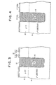
- Step 1 A p- doped monocrystalline silicon film 30 is grown epitaxially on p+ doped substrate 10.
- a composite layer 12 of Si0 2 and Si 3 N 4 is formed on epitaxial layer 30. After suitable lithography steps, an opening is made in composite layer 12. The composite layer 12 which remains is then used to mask the etch of a trench into substrate 10 by RIE (reactive ion etching) as shown in FIG. 3.
- RIE reactive ion etching
- Step 2 After a thin SiO 2 layer is thermally grown on the trench surface, a thin Si 3 N 4 layer is deposited and thermally densified in an oxidizing ambient to form composite film 16, the capacitor storage insulator. A thick, p+ doped polysilicon layer 18 is then deposited to fill the trench as shown in FIG. 3.
- Step 3 The polysilicon film 18 is planarized by RIE and/or chemical-mechanical polishing such that the surface of polysilicon 18 is coplanar with the top of substrate 10 as shown in FIG. 3.
- the nitride/oxide layer 12 over the substrate surface is used for etch stop.
- Step 4 An SiO 2 layer 34 is thermally grown on polysilicon 18. The presence of composite film 12 on the monocrystalline regions prevents oxidation of epitaxial layer 30 as shown in FIG 4.. The thickness of SiO 2 layer 34 is much greater than that of the SiO 2 portion of composite layer 12.
- Step 5 The Si 3 N 4 portion of composite layer 12 is removed by selective isotropic etching. The Si0 2 portion of composite layer 12 is then entirely removed, leaving a thickness of SiO 2 layer 34 on polysilicon 18 by virtue of its much greater thickness compared to the SiO 2 portion of composite layer 12.
- Step 6.'A monocrystalline, p-type doped layer 22 is grown epitaxially on the exposed surface of epitaxial layer 30 as shown in FIG. 5.
- Epitaxial layer 22 grows laterally over Si0 2 layer 34 at approximately the same rate as it grows vertically from epitaxial layer 30. In this way, the growth of epitaxial layer 22 is controlled to produce a lateral "window" 50 between its advancing edges over Si0 2 layer 34, illustrated by both top and cross section views.
- a silicon plug of p+ doped silicon can be formed in one of two alternative ways to establish contact to the polysilicon fill 18 of the trench storage capacitor.
- One technique will be described as Steps 7, 8 and 9; the other technique will be described as Steps 10, 11, 12, 13 and 14.
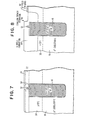
- Step 7 Aforesaid window 50 in epitaxial layer 22 is used as a self-aligned mask for removing Si0 2 layer 34 over polysilicon 18 in window area 50 by either wet chemical, dry plasma or reactive ion etching, as shown in FIG. 6.
- a contact region to the trench fill polysilicon 18 is established by a self-aligned epitaxial growth technique rather than by lithographic masking steps.
- Step 8 After opening the contact region, another epitaxial layer 24 is grown to fill window 50 as shown in FIG. 7. Note that during this growth a pyramidal region 52 of polycrystalline silicon called “neck” results in the window 50 area of polysilicon trench fill 18. Dopant diffuses from polysilicon trench fill 18 into the polycrystalline region 52 of epitaxial layer 24 during this step and subsequent heat treatments forms a conductive region between the polysilicon trench fill 18 and the wafer surface.
- Step 9 Isolation regions and p-channel FET devices are then fabricated in the conventional manner to produce the structure shown in FIG. 1, which is briefly described here.
- a composite layer of Si0 2 and Si 3 N 4 is formed on the substrate. After suitable lithography steps, an opening is made in the composite layer. The composite layer which remains is then used to mask the etch of a shallow trench 90 into layers 22 and 24 by RIE (reactive ion etching) as shown in FIG. 8.
- a thin p+ doped glass film 92 is deposited for field isolation of peripheral n-channel devices.
- a photoresist layer is applied and a mask is used to remove part of the photoresist and the underlying p+ glass layer to expose the regions for n-well formation.
- n-type dopants are implanted through the composite layer of Si0 2 and Si 3 N 4 on the substrate to form n-well 94 regions.
- Photoresist outside the n-well region blocks the n-type implantation into the n-channel device 92 regions.
- a short thermal cycle is used to drive in the p-type dopant into the substrate 30 and the p+ glass layer is removed.
- a thin thermal oxide is grown over the shallow trench 90 surface, followed by depositing a thick oxide layer to fill the shallow trench and planarization to result in a coplanar surface between the oxide isolation 96 and substrate surface as shown in FIG. 1.
- the composite layer of Si02 and S i 3N4 is removed.
- a thin layer of gate oxide is thermally grown with polysilicon gate deposited and defined over it. Form oxide spacer on gate electrode edge, and implant p-type and n-type dopants to obtain the source and drain junctions for p- and n-channel devices, respectively. Open surfaces of polysilicon gates and source/drain regions for subsequent self-aligned silicide formation, deposit blanket CVD glass form and reflow, etch contact holes, and deposit and pattern metal level to complete the cell structure as shown in FIG. 1.
- Step 10 The second approach to formation of the conductive plug comprises following the growth of epitaxial layer 22 (Step 6, FIG. 5) with oxidation of layer 22 to form Si0 2 layer 56 and by deposition of Si 3 N 4 layer 58 as shown in FIG. 9.
- Step 11 Layer 60 of phosphorus-doped n+ polysilicon is deposited on Si 3N4 layer 58 as shown in FIG. 10. With a very narrow contact window 50 as would be employed in VLSI DRAM, n+ polysilicon layer 60 will deposit on the top surface of Si 3 N 4 layer 58 and just over the corners, but will not deposit on oxidized trench fill polysilicon layer 34 at the bottom of window 50.
- Step 12 Using selective and anisotropic RIE, Si 3 N 4 layer 58, SiO 2 layer 56 and oxidized trench fill polysilicon layer 34 are removed from the bottom of window 50 as shown in FIG. 10, using n+ polysilicon layer 60 as a mask. Because of the anisotropic etch, SiO 2 layer 56 and Si 3 N 4 layer 58 remain on the sidewalls of window 50.
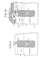
- Step 13 Deposit intrinsic polysilicon layer 62 to fill window 50 as shown in FIG. 10.
- Step 14 Planarize polysilicon layers 62 and 60, stopping on Si 3 N 4 layer 58, using RIE and/or chemi- cal/mechanical polishing. Remove Si 3 N 4 layer 58 and SiO 2 layer 56 from the top surface of epitaxial layer 22 as shown in FIG. 11. Doping of polysilicon plug layer 60 in window is assured by subsequent thermal processing steps required to complete the DRAM fabrication.
- Step 15 Conventional CMOS DRAM processing steps as described in Step 9 are performed to produce the memory cell structure shown in FIG. 12.'
- the self-aligned silicide 90 is continuously formed by deposition and annealing across Si0 2 layer 56 and S i 3 N 4 layer 58 between polysilicon plug layer 60 and the adjacent diffusion of the FET memory transistor to form a self-aligned electrical connection.
- the memory cell can be made n-channel without loss of generality by reversing the dopant polarity of polysilicon trench fill 18, forming an p-type "well" region in epitaxial layers 30, 22 and 52, and forming n-channel FET devices in the p-type well.
- the memory cell can be made n-channel outside the n-well region without loss of generality as shown in FIG. 13, by reversing the dopant polarity of polysilicon trench fill 18 and forming n-channel FE T as transfer devices.
- FIG. 14 illustrates a cross-sectional view of an inverter using a resistive load fabricated using the method of the present invention, with its equivalent circuit schematic as shown in FIG. 15.
- the structure of the device of FIG. 14 includes a silicon substrate 110 which, for the purposes of explanation, is n+ type.
- a n-channel transfer device with gate 180, source 198, and drain 184 is made in a p-well region 194 within a n-type epitaxial layer 130.
- a trench resistor is located in substrate 110 and filled with n-type doped polysilicon 118 which gives a suitable resistance value.
- a thick oxide film 116 on the trench sidewalls is provided for the insulator.
- An n+ doped vertical connection 152 is formed to connect the source region of the driver device and the resistive electrode 118,of the trench resistor.
- An interconnection 186 connected to the source region of the driver device is used as inverter output and an interconnection 182 which is connected to both the drain region of the driver device and a p+ region employed for applying a bias to the p-well is used for supplying the bias voltage to the inverter, such as ground in FIG. 14.
- Step Al A n- doped monocrystalline silicon film 130 is grown epitaxially on n+ doped substrate 110.
- a composite layer of Si0 2 and Si 3 N 4 is formed on epitaxial layer 130. After suitable lithography steps, an opening is made in composite layer. The portion of composite layer 112 which remains is then used to mask the etch of a trench into substrate 110 by RIE (reactive ion etching).
- Step A2 A thick Si0 2 layer 116 is thermally grown on the trench surface to form an insulator layer. Using selective and anisotropic RIE, only the Si0 2 layer at the bottom of trench is removed. Because of the anisotropic etch, SiO 2 layer 116 remains on the sidewalls of the trench, while the etch selectivity prevents attack of composite layer 112. A thick, n-type doped polysilicon layer 118 is then deposited to fill the trench. The n-type dopant level is chosen to give the desired resistance for the load device.
- Step A3 The polysilicon film 118 is planarized by RIE and/or chemical-mechanical polishing such that the surface of polysilicon 118 is coplanar with the top of epitaxial layer 130.
- Composite layer 112 over the substrate surface is used as the etch stop.
- Step A4 An SiO 2 layer 134 is thermally grown on polysilicon 118. The presence of composite film 112 on the monocrystalline regions prevents oxidation of epitaxial layer 130. The thickness of Si0 2 layer 134 is much greater than that of the SiO 2 portion of composite layer 112.
- Step A5. The Si 3 N 4 portion of composite layer 112 is removed by selective isotropic etching. The Si0 2 portion of composite layer 112 is then entirely removed, leaving a thickness of SiO 2 layer 134 on polysilicon 118 by virtue of its much greater thickness compared to the SiO 2 portion of composite layer.
- Step A6 A monocrystalline, n-type doped layer 122 is grown epitaxially on the exposed surface of epitaxial layer 130.
- Epitaxial layer 122 grows laterally over SiO 2 layer 134 at approximately the same rate as it grows vertically from epitaxial layer 130. In this way, the growth of epitaxial layer 122 is controlled to produce a lateral "window" between its advancing edges over Si0 2 layer 134.
- Step A7 Aforesaid window in epitaxial layer 122 is used as a self-aligned mask for removing Si0 2 layer 134 over polysilicon 118 in window area 150 by either wet chemical, dry plasma or reactive ion etching.
- a contact region to the trench fill polysilicon 118 is established by a self-aligned epitaxial growth technique rather than by lithographic masking steps.
- Step A8 After opening contact region, another epitaxial layer is grown to fill window. Note that during this growth a pyramidal region 152 of polycrystalline silicon, hereafter referred to as the "neck", results in the window area 150 of polysilicon trench fill 118. Dopant diffusion from polysilicon trench fill 118 into the polycrystalline region of epitaxial layer 152 during this step and subsequent heat treatments forms a conductive region between the polysilicon trench fill 118 and the wafer surface.
- Step A9 Isolation regions and n-channel FET devices are then fabricated in the conventional manner as described in Step 9 above with n-type dopant polarity. The complete cell structure as shown in FIG. 14.
- FIG. 16 shows several examples.
- the edges of the oxide cap 34 of a rectangular shape are aligned in the ⁇ 110> direction of a silicon substrate.
- Contact window 50 is a rectangle rotated 45 degrees with edges oriented mainly along the ⁇ 100> 'direction. If a T-shaped oxide cap is designed, the epitaxial layer closes over the narrow,portions of the T-shape, producing a window 50 over the widest portion of the T-shape as shown in FIG. 16(b).
- the window 50 can be mainly a rectangle, the directions of whose sides coincide with those of the oxide cap 34 (FIG. 16(c)). Orientation of the major axis of a T-shaped oxide cap 34 along the ⁇ 100> direction produces a contact window 50 positioned as in FIG. 16(b) but without rotation, as shown in FIG. 16(d).
- the processing techniques described can be used to form a self-aligned contact window in an epitaxial layer over an oxide-capped device structure. Subsequent formation of a self-aligned connection between the oxide-capped device and the device stacked over it produces a very compact stacked-device structure design.
- processing techniques as applied specifically to a three-dimensional stacked DRAM cell and a stacked inverter structure, provide self-alignment features which reduce fabrication cost and complexity by eliminating lithographic steps.
- control of the lateral growth of epitaxial layers 22 (or 122) and 52 (or 152) with respect to the larger sizes of etched trench features in substrate 10 (or 110) permits the use of unclosed windows in layers 22 (or 122) and 52 (or 152) over oxidized trench fill polysilicon layers 34 (or 134) as alignment-mark features at succeeding masking levels.
Abstract
Description
- The present invention relates to a fabrication method wherein an epitaxial layer is formed on a monocrystalline substrate such as silicon and over predefined insulator-capped features such that a self-aligned contact window and subsequent electrical connection can be made to the silicon region capped by the insulator.
- The following references are typical of the state of the art of DRAMs with trench capacitors.
- U.S. Patent 4,353,086 issued October 5, 1982 to Jaccodine et al entitled SILICON INTEGRATED CIRCUITS describes a dynamic random access memory in which individual cells, including an access transistor and a storage capacitor, are formed in mesas formed on a silicon chip. The access transistor of the cell is formed on the top surface of the mesa and one plate of the storage capacitor of the cell is formed by the sidewall of the mesa and the other plate by doped polycrystalline silicon which fills the grooves surrounding the mesas isolated therefrom by a silicon dioxide layer. By this geometry, large storage surfaces, and so large capacitances, can be obtained for the capacitor without using surface area of the chip. In other embodiments, the mesas may include other forms of circuit elements.
- U.S. Patent 4,327,47& issued May 4, 1982 to Iwai et al entitled METHOD OF MANUFACTURING SEMICONDUCTOR DEVICES describes a method which comprises the steps of: forming at least one groove at a given location of a semiconductor substrate; laying an insulating film over the entire surface of the semiconductor substrate including the groove; depositing conductive material on the insulating layer to a thickness greater than half the width of an opening of the groove; and forming a MOS capacitor electrode of the conductor layer left in the groove by etching the deposited conductor layer until the insulating film other than its portion within the groove is exposed.
- U.S. Patent 4,462,847 issued July 31, 1984 to Thompson et al entitled FABRICATION OF DIELECTRICALLY ISOLATED MICROELECTRONIC SEMICONDUCTOR CIRCUITS UTILIZING SELECTIVE GROWTH BY LOW PRESSURE VAPOR DEPOSITION describes a method for the fabrication of microelectronic semiconductor circuits, including the concurrent low pressure deposition of monocrystalline and polycrystalline semiconductor material in a predetermined pattern. A dielectric isolated circuit is fabricated, by such selective epitaxial growth, and a subsequent oxidation of both of the mono- and polycrystalline deposits. By controlling the ratio of the deposition rates, and by controlling the oxidation step, the poly deposit is substantially fully converted to oxide, while the mono is only partly oxidized, leaving a substantially coplanar, isolated matrix of passivated monocrystalline areas, in which to fabricate circuit components for interconnection.
- In Japanese Patent 58-137245, a technique is described to increase the area of an electrode without increasing the area of a plane by using the sidewall section of a groove dug into an Si substrate as the electrode surface of a capacitor. A field Si02 film is formed selectively onto a Si substrate through a LOCOS method, an etched groove is formed into the substrate and a capacitor insulating film made of si3N4 is shaped onto these surfaces through a CVD method. The whole surface of the insulating film is coated with a plate represented by polycrystalline Si. A groove is buried with the same polycrystalline Si at the time. The plate is oxidized and a first inter-layer oxide film is formed, the Si3N4 film and an SiO2 film are removed while using the oxide film as a mask, and a gate oxide film is formed through oxidation. A predetermined section is coated with a word line, and source-drain layers are formed to a section not coated with the plate and the gate through ion implantation, and a second inter-layer insulating film and the electrode are coated selectively.
- An object of the present invention is to provide an improved fabrication process for providing an epitaxial layer on a silicon substrate and over predefined insulator-capped islands which forms a self-aligned contact window in the epitaxial layer. Another object of the present invention is to provide an improved fabrication process for providing an connection between the device made in the epitaxial layer and the device below the predefined insulator-capped islands and forming a self-aligned contact-connection in the epitaxial layer.
- Another object of the present invention is to provide an improved one-transistor dynamic random-access-memory (DRAM) cell structure which has a single-crystal transistor stacked on top of a trench capacitor, and a fabrication method therefor.
- Another object of the present invention is to provide a fabrication method for a DRAM device wherein the contact window for the connection between the source region of the access transistor and the storage electrode of the trench capacitor is formed by controlled lateral epitaxial growth to provide a self-aligned contact window.
- Another object of the present invention is to provide a fabrication method for a DRAM device wherein the connection between the source region of the access transistor and the storage electrode of the trench capacitor is formed either by using a second-step epitaxial growth to provide a self-aligned contact connection or by using a conductor refill, planarization and strapping process.
- Another object of the present invention is to provide a fabrication method for a resistive-load inverter structure wherein the contact window for the connection between the resistor and the driver device is formed by controlled lateral epitaxial growth to provide a self-aligned contact window and followed by a connection formation step using a second epitaxial growth to fill the contact window.
-
- FIG. 1 is a schematic illustration of a cross section of an embodiment of a DRAM cell structure including an epitaxial layer with a self-aligned connection fabricated according to the principles of the present invention.
- FIG. 2 is a schematic illustration of a top view of an embodiment of the DRAM cell structure which is shown in FIG. 1.
- FIG. 3 is a schematic illustration of a cross section of a device being fabricated using the method.
- FIG. 4 is a schematic drawing illustrating a further step in the fabrication of a device using the method of the present invention.
- FIGS. 5 to 8 are schematic illustrations of a cross section of a device illustrating additional steps of the fabrication method according to the principles of the present invention.
- FIGS. 9 to 12 illustrate the fabrication of an alternative structure at various stages in another embodiment of a fabrication process according to the principles of the present invention.
- FIG. 13-is a schematic illustration of a cross section of an embodiment of an alternative DRAM cell structure including an epitaxial layer with a self-aligned connection fabricated according to the principles of the present invention.
- FIG. 14 is a schematic illustration of a cross section of an embodiment of an inverter structure having the driver device stacked over the load-resistor including an epitaxial layer with a self-aligned connection fabricated according to the principles of the present invention.
- FIG. 15 is a schematic illustration of the equivalent circuit of an embodiment of the inverter structure which is shown in FIG. 14.
- FIG. 16 shows the shape and position of self-aligned contact window on top of the oxide-capped features.
- The description of the fabrication method of the present invention is described relative to FIGS. 1 through 16.
- Application of the method to a three-dimensional dynamic random access memory (DRAM) device structure is shown, with an access transistor formed in monocrystalline silicon stacked on top of a trench capacitor. A fabrication method therefor is shown wherein the contact window for the source-to-trench connection is formed by self-aligned lateral epitaxial growth, followed by a contact-connection formation step using either a second epitaxial growth or a CVD refill and strapping process. The invention can be further applied to other device structures using the described principles, and more specifically to an inverter structure having the driver device stacked over the load-resistor as another example, which can be used as a basic building circuit unit for logic circuits and static-RAM cell.
- FIG. 1 illustrates a cross-sectional view of a DRAM cell fabricated using the method of the present invention illustrated in FIGS. 3, 4, 5, 6, 7, and 8, with a top view shown in FIG. 2. The structure of the device of FIG. 1 includes a
silicon substrate 10 which, for the purposes of explanation, is p+ type. A p-channel transfer device withgate 80,source 98, anddrain 84 is made in an n-well region 94 within a p-typeepitaxial layer 30. A trench capacitor is located insubstrate 10 and filled with heavily dopedp+ polysilicon 18. Acomposite film 16 of Si02/Si3N4/Si02 on the trench sidewalls is provided for the capacitor storage insulator. A p+ dopedvertical connection 52 is formed to connect.the source region of the transfer device and thestorage electrode 18 of the trench capacitor. Aninterconnection 82 used for the bitline is connected to the drain region of the transfer device. - The method steps of one embodiment of the present invention for fabricating the cell structure of FIG. 1 are described as follows.
-
Step 1. A p- dopedmonocrystalline silicon film 30 is grown epitaxially on p+ dopedsubstrate 10. Acomposite layer 12 of Si02 and Si3N4 is formed onepitaxial layer 30. After suitable lithography steps, an opening is made incomposite layer 12. Thecomposite layer 12 which remains is then used to mask the etch of a trench intosubstrate 10 by RIE (reactive ion etching) as shown in FIG. 3. - Step 2. After a thin SiO2 layer is thermally grown on the trench surface, a thin Si3N4 layer is deposited and thermally densified in an oxidizing ambient to form
composite film 16, the capacitor storage insulator. A thick, p+ dopedpolysilicon layer 18 is then deposited to fill the trench as shown in FIG. 3. - Step 3. The
polysilicon film 18 is planarized by RIE and/or chemical-mechanical polishing such that the surface ofpolysilicon 18 is coplanar with the top ofsubstrate 10 as shown in FIG. 3. The nitride/oxide layer 12 over the substrate surface is used for etch stop. - Step 4. An SiO2
layer 34 is thermally grown onpolysilicon 18. The presence ofcomposite film 12 on the monocrystalline regions prevents oxidation ofepitaxial layer 30 as shown in FIG 4..The thickness of SiO2 layer 34 is much greater than that of the SiO2 portion ofcomposite layer 12. - Step 5. The Si3N4 portion of
composite layer 12 is removed by selective isotropic etching. The Si02 portion ofcomposite layer 12 is then entirely removed, leaving a thickness of SiO2 layer 34 onpolysilicon 18 by virtue of its much greater thickness compared to the SiO2 portion ofcomposite layer 12. - Step 6.'A monocrystalline, p-type doped
layer 22 is grown epitaxially on the exposed surface ofepitaxial layer 30 as shown in FIG. 5.Epitaxial layer 22 grows laterally over Si02 layer 34 at approximately the same rate as it grows vertically fromepitaxial layer 30. In this way, the growth ofepitaxial layer 22 is controlled to produce a lateral "window" 50 between its advancing edges over Si02 layer 34, illustrated by both top and cross section views. - At this point, a silicon plug of p+ doped silicon can be formed in one of two alternative ways to establish contact to the polysilicon fill 18 of the trench storage capacitor. One technique will be described as Steps 7, 8 and 9; the other technique will be described as
Steps - Step 7.
Aforesaid window 50 inepitaxial layer 22 is used as a self-aligned mask for removing Si02 layer 34 overpolysilicon 18 inwindow area 50 by either wet chemical, dry plasma or reactive ion etching, as shown in FIG. 6. Thus, a contact region to the trench fillpolysilicon 18 is established by a self-aligned epitaxial growth technique rather than by lithographic masking steps. - Step 8. After opening the contact region, another
epitaxial layer 24 is grown to fillwindow 50 as shown in FIG. 7. Note that during this growth apyramidal region 52 of polycrystalline silicon called "neck" results in thewindow 50 area of polysilicon trench fill 18. Dopant diffuses from polysilicon trench fill 18 into thepolycrystalline region 52 ofepitaxial layer 24 during this step and subsequent heat treatments forms a conductive region between the polysilicon trench fill 18 and the wafer surface. - Step 9. Isolation regions and p-channel FET devices are then fabricated in the conventional manner to produce the structure shown in FIG. 1, which is briefly described here. A composite layer of Si02 and Si3N4 is formed on the substrate. After suitable lithography steps, an opening is made in the composite layer. The composite layer which remains is then used to mask the etch of a
shallow trench 90 intolayers glass film 92 is deposited for field isolation of peripheral n-channel devices. A photoresist layer is applied and a mask is used to remove part of the photoresist and the underlying p+ glass layer to expose the regions for n-well formation. Then n-type dopants are implanted through the composite layer of Si02 and Si3N4 on the substrate to form n-well 94 regions. Photoresist outside the n-well region blocks the n-type implantation into the n-channel device 92 regions. After the photoresist is removed, a short thermal cycle is used to drive in the p-type dopant into thesubstrate 30 and the p+ glass layer is removed. A thin thermal oxide is grown over theshallow trench 90 surface, followed by depositing a thick oxide layer to fill the shallow trench and planarization to result in a coplanar surface between theoxide isolation 96 and substrate surface as shown in FIG. 1. Then the composite layer of Si02 and Si3N4 is removed. A thin layer of gate oxide is thermally grown with polysilicon gate deposited and defined over it. Form oxide spacer on gate electrode edge, and implant p-type and n-type dopants to obtain the source and drain junctions for p- and n-channel devices, respectively. Open surfaces of polysilicon gates and source/drain regions for subsequent self-aligned silicide formation, deposit blanket CVD glass form and reflow, etch contact holes, and deposit and pattern metal level to complete the cell structure as shown in FIG. 1. - Note that, by virtue of dopant diffusion from polysilicon trench fill 18 into the polycrystalline region of
epitaxial layer 52 as described in Step 8 and high diffusivity of theneck 52, conventional formation of the shallow p-type diffusion for the source region of the FET is sufficient to establish an electrical connection between the source region of the FET and polysilicon trench fill 18 without additional lithographic patterning. This feature of the method provides significant advantage for decreasing memory cell area over previously described methods. -
Step 10. The second approach to formation of the conductive plug comprises following the growth of epitaxial layer 22 (Step 6, FIG. 5) with oxidation oflayer 22 to form Si02 layer 56 and by deposition of Si3N4 layer 58 as shown in FIG. 9. - Step 11.
Layer 60 of phosphorus-doped n+ polysilicon is deposited on Si3N4 layer 58 as shown in FIG. 10. With a verynarrow contact window 50 as would be employed in VLSI DRAM,n+ polysilicon layer 60 will deposit on the top surface of Si3N4 layer 58 and just over the corners, but will not deposit on oxidized trench fillpolysilicon layer 34 at the bottom ofwindow 50. -
Step 12. Using selective and anisotropic RIE, Si3N4 layer 58, SiO2 layer 56 and oxidized trench fillpolysilicon layer 34 are removed from the bottom ofwindow 50 as shown in FIG. 10, usingn+ polysilicon layer 60 as a mask. Because of the anisotropic etch, SiO2 layer 56 and Si3N4 layer 58 remain on the sidewalls ofwindow 50. - Step 13. Deposit
intrinsic polysilicon layer 62 to fillwindow 50 as shown in FIG. 10. -
Step 14. Planarize polysilicon layers 62 and 60, stopping on Si3N4 layer 58, using RIE and/or chemi- cal/mechanical polishing. Remove Si3N4 layer 58 and SiO2 layer 56 from the top surface ofepitaxial layer 22 as shown in FIG. 11. Doping ofpolysilicon plug layer 60 in window is assured by subsequent thermal processing steps required to complete the DRAM fabrication. - Step 15. Conventional CMOS DRAM processing steps as described in Step 9 are performed to produce the memory cell structure shown in FIG. 12.' The self-aligned
silicide 90 is continuously formed by deposition and annealing across Si02 layer 56 and Si3N4 layer 58 betweenpolysilicon plug layer 60 and the adjacent diffusion of the FET memory transistor to form a self-aligned electrical connection. - The memory cell can be made n-channel without loss of generality by reversing the dopant polarity of polysilicon trench fill 18, forming an p-type "well" region in
epitaxial layers - The memory cell can be made n-channel outside the n-well region without loss of generality as shown in FIG. 13, by reversing the dopant polarity of polysilicon trench fill 18 and forming n-channel FET as transfer devices.
- FIG. 14 illustrates a cross-sectional view of an inverter using a resistive load fabricated using the method of the present invention, with its equivalent circuit schematic as shown in FIG. 15. The structure of the device of FIG. 14 includes a
silicon substrate 110 which, for the purposes of explanation, is n+ type. A n-channel transfer device withgate 180,source 198, and drain 184 is made in a p-well region 194 within a n-type epitaxial layer 130. A trench resistor is located insubstrate 110 and filled with n-type dopedpolysilicon 118 which gives a suitable resistance value. Athick oxide film 116 on the trench sidewalls is provided for the insulator. An n+ dopedvertical connection 152 is formed to connect the source region of the driver device and theresistive electrode 118,of the trench resistor. Aninterconnection 186 connected to the source region of the driver device is used as inverter output and aninterconnection 182 which is connected to both the drain region of the driver device and a p+ region employed for applying a bias to the p-well is used for supplying the bias voltage to the inverter, such as ground in FIG. 14. - The method steps of one embodiment of the present invention for fabricating the inverter structure of FIG. 14 are described as follows.
- Step Al. A n- doped
monocrystalline silicon film 130 is grown epitaxially on n+doped substrate 110. A composite layer of Si02 and Si3N4 is formed onepitaxial layer 130. After suitable lithography steps, an opening is made in composite layer. The portion of composite layer 112 which remains is then used to mask the etch of a trench intosubstrate 110 by RIE (reactive ion etching). - Step A2. A thick Si02 layer 116 is thermally grown on the trench surface to form an insulator layer. Using selective and anisotropic RIE, only the Si02 layer at the bottom of trench is removed. Because of the anisotropic etch, SiO2 layer 116 remains on the sidewalls of the trench, while the etch selectivity prevents attack of composite layer 112. A thick, n-type doped
polysilicon layer 118 is then deposited to fill the trench. The n-type dopant level is chosen to give the desired resistance for the load device. - Step A3. The
polysilicon film 118 is planarized by RIE and/or chemical-mechanical polishing such that the surface ofpolysilicon 118 is coplanar with the top ofepitaxial layer 130. Composite layer 112 over the substrate surface is used as the etch stop. - Step A4. An SiO2 layer 134 is thermally grown on
polysilicon 118. The presence of composite film 112 on the monocrystalline regions prevents oxidation ofepitaxial layer 130. The thickness of Si02 layer 134 is much greater than that of the SiO2 portion of composite layer 112. - Step A5. The Si3N4 portion of composite layer 112 is removed by selective isotropic etching. The Si02 portion of composite layer 112 is then entirely removed, leaving a thickness of SiO2 layer 134 on
polysilicon 118 by virtue of its much greater thickness compared to the SiO2 portion of composite layer. - Step A6. A monocrystalline, n-type doped
layer 122 is grown epitaxially on the exposed surface ofepitaxial layer 130.Epitaxial layer 122 grows laterally over SiO2 layer 134 at approximately the same rate as it grows vertically fromepitaxial layer 130. In this way, the growth ofepitaxial layer 122 is controlled to produce a lateral "window" between its advancing edges over Si02 layer 134. - Step A7. Aforesaid window in
epitaxial layer 122 is used as a self-aligned mask for removing Si02 layer 134 overpolysilicon 118 in window area 150 by either wet chemical, dry plasma or reactive ion etching. Thus, a contact region to the trench fillpolysilicon 118 is established by a self-aligned epitaxial growth technique rather than by lithographic masking steps. - Step A8. After opening contact region, another epitaxial layer is grown to fill window. Note that during this growth a
pyramidal region 152 of polycrystalline silicon, hereafter referred to as the "neck", results in the window area 150 ofpolysilicon trench fill 118. Dopant diffusion from polysilicon trench fill 118 into the polycrystalline region ofepitaxial layer 152 during this step and subsequent heat treatments forms a conductive region between the polysilicon trench fill 118 and the wafer surface. - Step A9. Isolation regions and n-channel FET devices are then fabricated in the conventional manner as described in Step 9 above with n-type dopant polarity. The complete cell structure as shown in FIG. 14.
- Experimental results show that the shape and position of self-aligned
contact window 50 on top of the cappedoxide oxide layer oxide cap 34 of a rectangular shape are aligned in the <110> direction of a silicon substrate. Contactwindow 50 is a rectangle rotated 45 degrees with edges oriented mainly along the <100> 'direction. If a T-shaped oxide cap is designed, the epitaxial layer closes over the narrow,portions of the T-shape, producing awindow 50 over the widest portion of the T-shape as shown in FIG. 16(b). If the edges of arectangular oxide cap 34 are aligned in the <100> direction of a silicon substrate, thewindow 50 can be mainly a rectangle, the directions of whose sides coincide with those of the oxide cap 34 (FIG. 16(c)). Orientation of the major axis of a T-shapedoxide cap 34 along the <100> direction produces acontact window 50 positioned as in FIG. 16(b) but without rotation, as shown in FIG. 16(d). The processing techniques described can be used to form a self-aligned contact window in an epitaxial layer over an oxide-capped device structure. Subsequent formation of a self-aligned connection between the oxide-capped device and the device stacked over it produces a very compact stacked-device structure design. These processing techniques, as applied specifically to a three-dimensional stacked DRAM cell and a stacked inverter structure, provide self-alignment features which reduce fabrication cost and complexity by eliminating lithographic steps. Moreover, control of the lateral growth of epitaxial layers 22 (or 122) and 52 (or 152) with respect to the larger sizes of etched trench features in substrate 10 (or 110) permits the use of unclosed windows in layers 22 (or 122) and 52 (or 152) over oxidized trench fill polysilicon layers 34 (or 134) as alignment-mark features at succeeding masking levels.
Claims (12)
Priority Applications (1)
| Application Number | Priority Date | Filing Date | Title |
|---|---|---|---|
| AT87106472T ATE73962T1 (en) | 1986-10-03 | 1987-05-05 | MANUFACTURING PROCESSES FOR FORMING A SELF-ALIGNING CONTACT WINDOW AND CONNECTION IN AN EPITACTIC LAYER AND DEVICE STRUCTURES USING THIS PROCESS. |
Applications Claiming Priority (2)
| Application Number | Priority Date | Filing Date | Title |
|---|---|---|---|
| US06/915,310 US4728623A (en) | 1986-10-03 | 1986-10-03 | Fabrication method for forming a self-aligned contact window and connection in an epitaxial layer and device structures employing the method |
| US915310 | 1986-10-03 |
Publications (2)
| Publication Number | Publication Date |
|---|---|
| EP0262294A1 true EP0262294A1 (en) | 1988-04-06 |
| EP0262294B1 EP0262294B1 (en) | 1992-03-18 |
Family
ID=25435545
Family Applications (1)
| Application Number | Title | Priority Date | Filing Date |
|---|---|---|---|
| EP87106472A Expired - Lifetime EP0262294B1 (en) | 1986-10-03 | 1987-05-05 | A fabrication method for forming a selfaligned contact window and connection in an epitaxial layer and device structures employing the method |
Country Status (9)
| Country | Link |
|---|---|
| US (1) | US4728623A (en) |
| EP (1) | EP0262294B1 (en) |
| JP (1) | JPS63127564A (en) |
| AT (1) | ATE73962T1 (en) |
| AU (1) | AU594200B2 (en) |
| CA (1) | CA1244559A (en) |
| DE (1) | DE3777514D1 (en) |
| ES (1) | ES2031083T3 (en) |
| MX (1) | MX165273B (en) |
Cited By (4)
| Publication number | Priority date | Publication date | Assignee | Title |
|---|---|---|---|---|
| EP0272491A2 (en) * | 1986-12-22 | 1988-06-29 | Texas Instruments Incorporated | Deep trench isolation with surface contact to substrate |
| EP0302204A2 (en) * | 1987-08-03 | 1989-02-08 | International Business Machines Corporation | Vertical trench transistor/capacitor memory cell structure and fabrication method therefor |
| EP1041623A2 (en) * | 1999-03-31 | 2000-10-04 | Infineon Technologies North America Corp. | An isolation collar nitride liner for DRAM process improvement |
| WO2001017019A2 (en) * | 1999-08-30 | 2001-03-08 | Infineon Technologies Ag | Memory with a trench capacitor and a selection transistor and method for producing the same |
Families Citing this family (64)
| Publication number | Priority date | Publication date | Assignee | Title |
|---|---|---|---|---|
| US4918502A (en) * | 1986-11-28 | 1990-04-17 | Hitachi, Ltd. | Semiconductor memory having trench capacitor formed with sheath electrode |
| US4980747A (en) * | 1986-12-22 | 1990-12-25 | Texas Instruments Inc. | Deep trench isolation with surface contact to substrate |
| JPH0795568B2 (en) * | 1987-04-27 | 1995-10-11 | 日本電気株式会社 | Semiconductor memory device |
| JPH0810757B2 (en) * | 1987-05-25 | 1996-01-31 | 松下電子工業株式会社 | Method for manufacturing semiconductor device |
| US5046043A (en) * | 1987-10-08 | 1991-09-03 | National Semiconductor Corporation | Ferroelectric capacitor and memory cell including barrier and isolation layers |
| US4942554A (en) * | 1987-11-26 | 1990-07-17 | Siemens Aktiengesellschaft | Three-dimensional, one-transistor cell arrangement for dynamic semiconductor memories comprising trench capacitor and method for manufacturing same |
| US5100823A (en) * | 1988-02-29 | 1992-03-31 | Motorola, Inc. | Method of making buried stacked transistor-capacitor |
| US5200354A (en) * | 1988-07-22 | 1993-04-06 | Hyundai Electronics Industries Co. Ltd. | Method for manufacturing dynamic random access memory cell |
| KR910007181B1 (en) * | 1988-09-22 | 1991-09-19 | 현대전자산업 주식회사 | Side-wall doped trench and stacked capacitor cell and method manufacturing thereof |
| JPH02135776A (en) * | 1988-11-17 | 1990-05-24 | Hitachi Ltd | Semiconductor storage device |
| US4962365A (en) * | 1989-03-30 | 1990-10-09 | Texas Instruments Incorporated | Integrated circuit trench resistor |
| US4954854A (en) * | 1989-05-22 | 1990-09-04 | International Business Machines Corporation | Cross-point lightly-doped drain-source trench transistor and fabrication process therefor |
| US5021355A (en) * | 1989-05-22 | 1991-06-04 | International Business Machines Corporation | Method of fabricating cross-point lightly-doped drain-source trench transistor |
| JPH0834298B2 (en) * | 1989-06-19 | 1996-03-29 | シャープ株式会社 | Semiconductor device and method of manufacturing semiconductor device |
| US5316962A (en) * | 1989-08-15 | 1994-05-31 | Matsushita Electric Industrial Co., Ltd. | Method of producing a semiconductor device having trench capacitors and vertical switching transistors |
| US5064777A (en) * | 1990-06-28 | 1991-11-12 | International Business Machines Corporation | Fabrication method for a double trench memory cell device |
| US5034787A (en) * | 1990-06-28 | 1991-07-23 | International Business Machines Corporation | Structure and fabrication method for a double trench memory cell device |
| US4988637A (en) * | 1990-06-29 | 1991-01-29 | International Business Machines Corp. | Method for fabricating a mesa transistor-trench capacitor memory cell structure |
| US5204281A (en) * | 1990-09-04 | 1993-04-20 | Motorola, Inc. | Method of making dynamic random access memory cell having a trench capacitor |
| US5198995A (en) * | 1990-10-30 | 1993-03-30 | International Business Machines Corporation | Trench-capacitor-one-transistor storage cell and array for dynamic random access memories |
| US5055898A (en) * | 1991-04-30 | 1991-10-08 | International Business Machines Corporation | DRAM memory cell having a horizontal SOI transfer device disposed over a buried storage node and fabrication methods therefor |
| US5214603A (en) * | 1991-08-05 | 1993-05-25 | International Business Machines Corporation | Folded bitline, ultra-high density dynamic random access memory having access transistors stacked above trench storage capacitors |
| JPH05211239A (en) * | 1991-09-12 | 1993-08-20 | Texas Instr Inc <Ti> | Interconnection structure of integrated circuit and method for formation of it |
| US5264716A (en) * | 1992-01-09 | 1993-11-23 | International Business Machines Corporation | Diffused buried plate trench dram cell array |
| US5399516A (en) * | 1992-03-12 | 1995-03-21 | International Business Machines Corporation | Method of making shadow RAM cell having a shallow trench EEPROM |
| US5314837A (en) * | 1992-06-08 | 1994-05-24 | Analog Devices, Incorporated | Method of making a registration mark on a semiconductor |
| CA2074848C (en) * | 1992-07-29 | 1998-02-10 | Joseph P. Ellul | Method of forming electrodes for trench capacitors |
| US5365097A (en) * | 1992-10-05 | 1994-11-15 | International Business Machines Corporation | Vertical epitaxial SOI transistor, memory cell and fabrication methods |
| JP2791260B2 (en) * | 1993-03-01 | 1998-08-27 | 株式会社東芝 | Method for manufacturing semiconductor device |
| JPH06252153A (en) * | 1993-03-01 | 1994-09-09 | Toshiba Corp | Manufacture of semiconductor device |
| US5641694A (en) * | 1994-12-22 | 1997-06-24 | International Business Machines Corporation | Method of fabricating vertical epitaxial SOI transistor |
| US5677219A (en) * | 1994-12-29 | 1997-10-14 | Siemens Aktiengesellschaft | Process for fabricating a DRAM trench capacitor |
| US5851923A (en) * | 1996-01-18 | 1998-12-22 | Micron Technology, Inc. | Integrated circuit and method for forming and integrated circuit |
| US6103627A (en) * | 1996-02-21 | 2000-08-15 | Micron Technology, Inc. | Treatment of a surface having an exposed silicon/silica interface |
| US5792685A (en) * | 1996-02-22 | 1998-08-11 | Siemens Aktiengesellschaft | Three-dimensional device layout having a trench capacitor |
| US5793075A (en) * | 1996-07-30 | 1998-08-11 | International Business Machines Corporation | Deep trench cell capacitor with inverting counter electrode |
| US5843820A (en) * | 1997-09-29 | 1998-12-01 | Vanguard International Semiconductor Corporation | Method of fabricating a new dynamic random access memory (DRAM) cell having a buried horizontal trench capacitor |
| JPH11186514A (en) * | 1997-12-22 | 1999-07-09 | Toshiba Corp | Manufacture of semiconductor storage device |
| KR100347544B1 (en) | 1999-02-13 | 2002-08-07 | 주식회사 하이닉스반도체 | Method of manufacturing a junction in a semiconductor device |
| US6140175A (en) * | 1999-03-03 | 2000-10-31 | International Business Machines Corporation | Self-aligned deep trench DRAM array device |
| KR100314276B1 (en) | 1999-04-12 | 2001-11-15 | 박종섭 | Method of manufacturing a semiconductor device |
| KR100353526B1 (en) | 1999-06-18 | 2002-09-19 | 주식회사 하이닉스반도체 | method for manufacturing semiconductor device |
| KR100345681B1 (en) | 1999-06-24 | 2002-07-27 | 주식회사 하이닉스반도체 | Method of fabricating triple well of semiconductor device using SEG |
| KR100332119B1 (en) | 1999-06-28 | 2002-04-10 | 박종섭 | Method of manufacturing a semiconductor device |
| KR100332108B1 (en) | 1999-06-29 | 2002-04-10 | 박종섭 | Transistor in a semiconductor device and method of manufacuring the same |
| KR100332107B1 (en) | 1999-06-29 | 2002-04-10 | 박종섭 | Method of manufacturing a transistor in a semiconductor device |
| KR100301246B1 (en) | 1999-06-30 | 2001-11-01 | 박종섭 | Method of manufacturing a semiconductor device |
| US6320215B1 (en) | 1999-07-22 | 2001-11-20 | International Business Machines Corporation | Crystal-axis-aligned vertical side wall device |
| KR20010061029A (en) | 1999-12-28 | 2001-07-07 | 박종섭 | A method for forming MOSFET of elevated source/drain structure |
| KR100510996B1 (en) | 1999-12-30 | 2005-08-31 | 주식회사 하이닉스반도체 | Method for optimizing processes of selective epitaxial growth |
| KR100327596B1 (en) | 1999-12-31 | 2002-03-15 | 박종섭 | Method for fabricating contact plug of semiconductor device using Selective Epitaxial Growth of silicon process |
| FR2819632B1 (en) * | 2001-01-12 | 2003-09-26 | St Microelectronics Sa | INTEGRATED CIRCUIT COMPRISING AN ANALOGUE CHARGE STORAGE DEVICE, AND MANUFACTURING METHOD |
| US6998305B2 (en) * | 2003-01-24 | 2006-02-14 | Asm America, Inc. | Enhanced selectivity for epitaxial deposition |
| US7633110B2 (en) * | 2004-09-21 | 2009-12-15 | Taiwan Semiconductor Manufacturing Co., Ltd. | Memory cell |
| US7402487B2 (en) * | 2004-10-18 | 2008-07-22 | Infineon Technologies Richmond, Lp | Process for fabricating a semiconductor device having deep trench structures |
| US8278176B2 (en) * | 2006-06-07 | 2012-10-02 | Asm America, Inc. | Selective epitaxial formation of semiconductor films |
| US7755926B2 (en) * | 2007-06-13 | 2010-07-13 | International Business Machines Corporation | 3-D SRAM array to improve stability and performance |
| US20080310220A1 (en) * | 2007-06-13 | 2008-12-18 | International Business Machines Corporation | 3-d sram array to improve stability and performance |
| US7759199B2 (en) * | 2007-09-19 | 2010-07-20 | Asm America, Inc. | Stressor for engineered strain on channel |
| US8367528B2 (en) * | 2009-11-17 | 2013-02-05 | Asm America, Inc. | Cyclical epitaxial deposition and etch |
| US8809170B2 (en) | 2011-05-19 | 2014-08-19 | Asm America Inc. | High throughput cyclical epitaxial deposition and etch process |
| US9852902B2 (en) | 2014-10-03 | 2017-12-26 | Applied Materials, Inc. | Material deposition for high aspect ratio structures |
| US9401410B2 (en) * | 2014-11-26 | 2016-07-26 | Texas Instruments Incorporated | Poly sandwich for deep trench fill |
| CN113130510B (en) * | 2019-11-22 | 2023-06-13 | 长江存储科技有限责任公司 | Memory device and hybrid spacer thereof |
Citations (1)
| Publication number | Priority date | Publication date | Assignee | Title |
|---|---|---|---|---|
| EP0167764A2 (en) * | 1984-06-14 | 1986-01-15 | International Business Machines Corporation | Dynamic ram cell |
Family Cites Families (7)
| Publication number | Priority date | Publication date | Assignee | Title |
|---|---|---|---|---|
| JPS5539677A (en) * | 1978-09-14 | 1980-03-19 | Chiyou Lsi Gijutsu Kenkyu Kumiai | Semiconductor device and its manufacturing |
| JPS5681968A (en) * | 1979-12-07 | 1981-07-04 | Toshiba Corp | Manufacture of semiconductor device |
| US4353086A (en) * | 1980-05-07 | 1982-10-05 | Bell Telephone Laboratories, Incorporated | Silicon integrated circuits |
| US4462847A (en) * | 1982-06-21 | 1984-07-31 | Texas Instruments Incorporated | Fabrication of dielectrically isolated microelectronic semiconductor circuits utilizing selective growth by low pressure vapor deposition |
| US4522661A (en) * | 1983-06-24 | 1985-06-11 | The United States Of America As Represented By The Administrator Of The National Aeronautics And Space Administration | Low defect, high purity crystalline layers grown by selective deposition |
| US4578142A (en) * | 1984-05-10 | 1986-03-25 | Rca Corporation | Method for growing monocrystalline silicon through mask layer |
| US4649625A (en) * | 1985-10-21 | 1987-03-17 | International Business Machines Corporation | Dynamic memory device having a single-crystal transistor on a trench capacitor structure and a fabrication method therefor |
-
1986
- 1986-10-03 US US06/915,310 patent/US4728623A/en not_active Expired - Fee Related
-
1987
- 1987-05-05 ES ES198787106472T patent/ES2031083T3/en not_active Expired - Lifetime
- 1987-05-05 EP EP87106472A patent/EP0262294B1/en not_active Expired - Lifetime
- 1987-05-05 DE DE8787106472T patent/DE3777514D1/en not_active Expired - Fee Related
- 1987-05-05 AT AT87106472T patent/ATE73962T1/en not_active IP Right Cessation
- 1987-07-20 JP JP62179280A patent/JPS63127564A/en active Granted
- 1987-09-24 CA CA000547694A patent/CA1244559A/en not_active Expired
- 1987-10-01 AU AU79268/87A patent/AU594200B2/en not_active Ceased
- 1987-10-02 MX MX008675A patent/MX165273B/en unknown
Patent Citations (1)
| Publication number | Priority date | Publication date | Assignee | Title |
|---|---|---|---|---|
| EP0167764A2 (en) * | 1984-06-14 | 1986-01-15 | International Business Machines Corporation | Dynamic ram cell |
Non-Patent Citations (4)
| Title |
|---|
| IBM TECHNICAL DISCLOSURE BULLETIN, vol. 21, no. 4, September 1978, pages 1552-1553, New York, US; D.L. BERGERON et al.: "Upside-down reach-through collector" * |
| INTERNATIONAL ELECTRON DEVICES MEETING, Washington, D.C., 1st-4th December 1985, pages 714-717, IEEE; W.F. RICHARDSON et al.: "A trench transistor cross-point dram cell" * |
| PROCEEDINGS OF THE IEEE, vol. 70, no. 5, May 1982, pages 420-457, New York, US; K.E. PETERSEN: "Silicon as a mechanical material" * |
| SOLID STATE TECHNOLOGY, vol. 27, no. 9, September 1984, pages 239-243, Port Washington, New York, US; L. JASTRZEBSKI: "Silicon CVD for SOI: principles and possible applications" * |
Cited By (9)
| Publication number | Priority date | Publication date | Assignee | Title |
|---|---|---|---|---|
| EP0272491A2 (en) * | 1986-12-22 | 1988-06-29 | Texas Instruments Incorporated | Deep trench isolation with surface contact to substrate |
| EP0272491A3 (en) * | 1986-12-22 | 1989-03-15 | Texas Instruments Incorporated | Deep trench isolation with surface contact to substrate |
| EP0302204A2 (en) * | 1987-08-03 | 1989-02-08 | International Business Machines Corporation | Vertical trench transistor/capacitor memory cell structure and fabrication method therefor |
| EP0302204A3 (en) * | 1987-08-03 | 1989-10-11 | International Business Machines Corporation | Vertical trench transistor/capacitor memory cell structure and fabrication method therefor |
| EP1041623A2 (en) * | 1999-03-31 | 2000-10-04 | Infineon Technologies North America Corp. | An isolation collar nitride liner for DRAM process improvement |
| EP1041623A3 (en) * | 1999-03-31 | 2001-04-11 | Infineon Technologies North America Corp. | An isolation collar nitride liner for DRAM process improvement |
| WO2001017019A2 (en) * | 1999-08-30 | 2001-03-08 | Infineon Technologies Ag | Memory with a trench capacitor and a selection transistor and method for producing the same |
| WO2001017019A3 (en) * | 1999-08-30 | 2001-05-10 | Infineon Technologies Ag | Memory with a trench capacitor and a selection transistor and method for producing the same |
| US6664167B2 (en) | 1999-08-30 | 2003-12-16 | Infineon Technologies Ag | Memory with trench capacitor and selection transistor and method for fabricating it |
Also Published As
| Publication number | Publication date |
|---|---|
| AU7926887A (en) | 1988-04-14 |
| ES2031083T3 (en) | 1992-12-01 |
| JPH0371787B2 (en) | 1991-11-14 |
| DE3777514D1 (en) | 1992-04-23 |
| CA1244559A (en) | 1988-11-08 |
| EP0262294B1 (en) | 1992-03-18 |
| AU594200B2 (en) | 1990-03-01 |
| JPS63127564A (en) | 1988-05-31 |
| US4728623A (en) | 1988-03-01 |
| MX165273B (en) | 1992-11-04 |
| ATE73962T1 (en) | 1992-04-15 |
Similar Documents
| Publication | Publication Date | Title |
|---|---|---|
| US4728623A (en) | Fabrication method for forming a self-aligned contact window and connection in an epitaxial layer and device structures employing the method | |
| US4833516A (en) | High density memory cell structure having a vertical trench transistor self-aligned with a vertical trench capacitor and fabrication methods therefor | |
| US4816884A (en) | High density vertical trench transistor and capacitor memory cell structure and fabrication method therefor | |
| US4649625A (en) | Dynamic memory device having a single-crystal transistor on a trench capacitor structure and a fabrication method therefor | |
| US5364810A (en) | Methods of forming a vertical field-effect transistor and a semiconductor memory cell | |
| US5410176A (en) | Integrated circuit with planarized shallow trench isolation | |
| US5055898A (en) | DRAM memory cell having a horizontal SOI transfer device disposed over a buried storage node and fabrication methods therefor | |
| US5324960A (en) | Dual-transistor structure and method of formation | |
| US5489790A (en) | Static-random-access memory cell | |
| US7897460B2 (en) | Methods of forming recessed access devices associated with semiconductor constructions | |
| KR0167811B1 (en) | Dram cell fabrication method | |
| US6767789B1 (en) | Method for interconnection between transfer devices and storage capacitors in memory cells and device formed thereby | |
| US5937296A (en) | Memory cell that includes a vertical transistor and a trench capacitor | |
| JP2994239B2 (en) | SOI trench structure and method of manufacturing the same | |
| US6294412B1 (en) | Silicon based lateral tunneling memory cell | |
| US4654121A (en) | Fabrication process for aligned and stacked CMOS devices | |
| US6309924B1 (en) | Method of forming self-limiting polysilicon LOCOS for DRAM cell | |
| US4939104A (en) | Method for forming a buried lateral contact | |
| US6472702B1 (en) | Deep trench DRAM with SOI and STI | |
| US6097061A (en) | Trenched gate metal oxide semiconductor device and method | |
| US5179038A (en) | High density trench isolation for MOS circuits | |
| US20060134898A1 (en) | Semiconductor damascene trench and methods thereof | |
| US5534457A (en) | Method of forming a stacked capacitor with an "I" shaped storage node | |
| JP2819520B2 (en) | DRAM cell | |
| JPS62118566A (en) | Manufacture of semiconductor memory |
Legal Events
| Date | Code | Title | Description |
|---|---|---|---|
| PUAI | Public reference made under article 153(3) epc to a published international application that has entered the european phase |
Free format text: ORIGINAL CODE: 0009012 |
|
| AK | Designated contracting states |
Kind code of ref document: A1 Designated state(s): AT CH DE ES FR GB IT LI NL SE |
|
| 17P | Request for examination filed |
Effective date: 19880823 |
|
| 17Q | First examination report despatched |
Effective date: 19901018 |
|
| GRAA | (expected) grant |
Free format text: ORIGINAL CODE: 0009210 |
|
| AK | Designated contracting states |
Kind code of ref document: B1 Designated state(s): AT CH DE ES FR GB IT LI NL SE |
|
| PG25 | Lapsed in a contracting state [announced via postgrant information from national office to epo] |
Ref country code: SE Effective date: 19920318 Ref country code: NL Effective date: 19920318 Ref country code: AT Effective date: 19920318 |
|
| REF | Corresponds to: |
Ref document number: 73962 Country of ref document: AT Date of ref document: 19920415 Kind code of ref document: T |
|
| REF | Corresponds to: |
Ref document number: 3777514 Country of ref document: DE Date of ref document: 19920423 |
|
| PGFP | Annual fee paid to national office [announced via postgrant information from national office to epo] |
Ref country code: SE Payment date: 19920427 Year of fee payment: 6 |
|
| ITF | It: translation for a ep patent filed |
Owner name: IBM - DR. ALFREDO BRAVI |
|
| PG25 | Lapsed in a contracting state [announced via postgrant information from national office to epo] |
Ref country code: LI Effective date: 19920531 Ref country code: CH Effective date: 19920531 |
|
| ET | Fr: translation filed | ||
| NLV1 | Nl: lapsed or annulled due to failure to fulfill the requirements of art. 29p and 29m of the patents act | ||
| REG | Reference to a national code |
Ref country code: ES Ref legal event code: FG2A Ref document number: 2031083 Country of ref document: ES Kind code of ref document: T3 |
|
| PLBE | No opposition filed within time limit |
Free format text: ORIGINAL CODE: 0009261 |
|
| STAA | Information on the status of an ep patent application or granted ep patent |
Free format text: STATUS: NO OPPOSITION FILED WITHIN TIME LIMIT |
|
| REG | Reference to a national code |
Ref country code: CH Ref legal event code: PL |
|
| 26N | No opposition filed | ||
| PGFP | Annual fee paid to national office [announced via postgrant information from national office to epo] |
Ref country code: GB Payment date: 19950413 Year of fee payment: 9 |
|
| PGFP | Annual fee paid to national office [announced via postgrant information from national office to epo] |
Ref country code: FR Payment date: 19950427 Year of fee payment: 9 |
|
| PGFP | Annual fee paid to national office [announced via postgrant information from national office to epo] |
Ref country code: ES Payment date: 19950523 Year of fee payment: 9 |
|
| PGFP | Annual fee paid to national office [announced via postgrant information from national office to epo] |
Ref country code: DE Payment date: 19950524 Year of fee payment: 9 |
|
| PG25 | Lapsed in a contracting state [announced via postgrant information from national office to epo] |
Ref country code: GB Effective date: 19960505 |
|
| PG25 | Lapsed in a contracting state [announced via postgrant information from national office to epo] |
Ref country code: ES Free format text: LAPSE BECAUSE OF NON-PAYMENT OF DUE FEES Effective date: 19960506 |
|
| GBPC | Gb: european patent ceased through non-payment of renewal fee |
Effective date: 19960505 |
|
| PG25 | Lapsed in a contracting state [announced via postgrant information from national office to epo] |
Ref country code: FR Effective date: 19970131 |
|
| PG25 | Lapsed in a contracting state [announced via postgrant information from national office to epo] |
Ref country code: DE Effective date: 19970201 |
|
| REG | Reference to a national code |
Ref country code: FR Ref legal event code: ST |
|
| REG | Reference to a national code |
Ref country code: ES Ref legal event code: FD2A Effective date: 19970611 |
|
| PG25 | Lapsed in a contracting state [announced via postgrant information from national office to epo] |
Ref country code: IT Free format text: LAPSE BECAUSE OF NON-PAYMENT OF DUE FEES;WARNING: LAPSES OF ITALIAN PATENTS WITH EFFECTIVE DATE BEFORE 2007 MAY HAVE OCCURRED AT ANY TIME BEFORE 2007. THE CORRECT EFFECTIVE DATE MAY BE DIFFERENT FROM THE ONE RECORDED. Effective date: 20050505 |