EP0265218B1 - Vector modulators and calibration thereof - Google Patents
Vector modulators and calibration thereof Download PDFInfo
- Publication number
- EP0265218B1 EP0265218B1 EP87309238A EP87309238A EP0265218B1 EP 0265218 B1 EP0265218 B1 EP 0265218B1 EP 87309238 A EP87309238 A EP 87309238A EP 87309238 A EP87309238 A EP 87309238A EP 0265218 B1 EP0265218 B1 EP 0265218B1
- Authority
- EP
- European Patent Office
- Prior art keywords
- output
- signals
- amplitude
- signal
- mixers
- Prior art date
- Legal status (The legal status is an assumption and is not a legal conclusion. Google has not performed a legal analysis and makes no representation as to the accuracy of the status listed.)
- Expired - Lifetime
Links
Images


Classifications
-
- H—ELECTRICITY
- H04—ELECTRIC COMMUNICATION TECHNIQUE
- H04L—TRANSMISSION OF DIGITAL INFORMATION, e.g. TELEGRAPHIC COMMUNICATION
- H04L27/00—Modulated-carrier systems
- H04L27/32—Carrier systems characterised by combinations of two or more of the types covered by groups H04L27/02, H04L27/10, H04L27/18 or H04L27/26
- H04L27/34—Amplitude- and phase-modulated carrier systems, e.g. quadrature-amplitude modulated carrier systems
- H04L27/36—Modulator circuits; Transmitter circuits
- H04L27/362—Modulation using more than one carrier, e.g. with quadrature carriers, separately amplitude modulated
- H04L27/364—Arrangements for overcoming imperfections in the modulator, e.g. quadrature error or unbalanced I and Q levels
-
- G—PHYSICS
- G01—MEASURING; TESTING
- G01R—MEASURING ELECTRIC VARIABLES; MEASURING MAGNETIC VARIABLES
- G01R35/00—Testing or calibrating of apparatus covered by the other groups of this subclass
- G01R35/005—Calibrating; Standards or reference devices, e.g. voltage or resistance standards, "golden" references
-
- H—ELECTRICITY
- H04—ELECTRIC COMMUNICATION TECHNIQUE
- H04L—TRANSMISSION OF DIGITAL INFORMATION, e.g. TELEGRAPHIC COMMUNICATION
- H04L27/00—Modulated-carrier systems
- H04L27/0014—Carrier regulation
- H04L2027/0016—Stabilisation of local oscillators
-
- H—ELECTRICITY
- H04—ELECTRIC COMMUNICATION TECHNIQUE
- H04L—TRANSMISSION OF DIGITAL INFORMATION, e.g. TELEGRAPHIC COMMUNICATION
- H04L27/00—Modulated-carrier systems
- H04L27/0014—Carrier regulation
- H04L2027/0018—Arrangements at the transmitter end
Definitions
- the invention relates to vector or quadrature (I/Q) modulators and the calibration thereof, in particular to calibration of a vector modulator using only one scalar detector.
- a major trend in microwave communications is the switch to digital communication, using digital modulation techniques. These techniques require a newclass of signal modulators which perform vector or quadrature modulation.
- vector modulation two modulation input signals independently modulate the in-phase (I) and quadrature (Q) components of the carrier.
- I and Q channels of the modulator must be calibrated to be equal in gain, i.e., balanced, and precisely 90° apart, i.e., in quadrature.
- One way to calibrate a vector modulator is with a network analyzer connected to the RF carrier input and to the RF modulated output.
- the network analyzer measures the amplitude and phase of the RF modulated output resulting from varying DC voltages applied to the I and Q modulation inputs. From these measurements, the gain and phase accuracy of the modulator can be determined, and calibrated.
- the drawback with the method is that it is an expensive and somewhat cumbersome solution, and therefore it does not lend itself to incorporation into a vector modulator for self calibration. It is also limited in accuracy for most network analyzers.
- An object of the present invention is to provide apparatus and a method for calibrating a vector modulator that does not require a network analyzer, and which improves the accuracy of the calibration measurement and makes the calibration system compact and inexpensive enough to be incorporated in the vector modulator for self calibration.
- the present invention provides a system comprising a standard vector modulator circuit modified by adding phase shifters to adjust the relative phases of the I and Q components of the RF carrier.
- Variable attenuators are inserted in the I and Q modulation signal input lines to adjust the relative amplitude of the modulation signals.
- Calibration measurements are made using a scalar detector to measure the amplitude of the RF output signal.
- Two DC signal sources provides reference signals for the I and Q modulation inputs.
- Two other DC signal sources provide carrier leak compensation signals.
- a final DC signal source provides calibration signals for balancing the amplitude of the I and Q modulation signals.
- the quadrature phase error is minimized by adjusting the phase shifters.
- the carrier leakage is minimized by adjusting the carrier leak compensation sources to minimize RF output with the modulation inputs grounded.
- the amplitudes of the I and Q modulation signals are balanced by adjusting the attenuators until the output amplitudes are equal.
- the quadrature calibration signal sources are adjusted until the output amplitudes they produce are balanced. This series of adjustments is repeated until no further changes are observed.
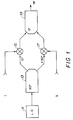
- Figure 1 shows a schematic block diagram of a vector modulator.
- Figure 2 shows a schematic block diagram of a vector modulator incorporating the calibration system of the invention.
- Figure 3 illustrates the theory of operation of vector modulators and the calibration technique of the invention. The proper operation of a vector modulator is shown in Figure 3A.
- Figure 3B illustrates the result when the I and Q channels are not exactly a t quadrature.
- Figure 3C illustrates the result when the I and Q channels are 90° out of phase, but they are not balanced.
- a vector modulator (also referred to as an I/Q modulator) applies two separate modulation signals to modulate the in-phase (I) and quadrature (Q) components of a carrier signal.
- Figure 1 shows a schematic block diagram of a typical vector modulator.
- An RF carrier signal generated by local oscillator 11 is divided into I and Q components by a 90° power divider 13.
- the I component with a phase defined as 0° is applied to the LO input of mixer 15.
- the I channel modulation signal is applied to another input of mixer 15 to produce a modulated I signal.
- the Q component with a 90° phase difference from the I component, is applied to an input of mixer 17.
- the Q channel modulation signal is applied to another input of mixer 17 to produce a modulated Q signal.
- the modulated I and Q signals are combined by a 0° power combiner 19 to produce the vector modulated RF output signal.
- the principal errors in the vector modulated signals produced by this modulator design can be attributed to carrier leakage, amplitude imbalance of the I and Q channels, and quadrature phase error.
- Carrier leakage is the appearance of an output signal from the mixers even when the modulation inputs are grounded. This can be caused by a non-zero offset voltage in a mixer, capacitive or inductive coupling of the LO signal across the mixer, and impedance mismatches at the mixer ports. Amplitude imbalance is caused by the differences in conversion losses of the I and Q mixers. Phase quadrature errors are due to miscalibration (design tolerances) of the 90° power splitter and the 0° power combiner, and to differences in the electrical path length of the I and Q channels.
- mixer 215 in Figure 2 is functionally equivalent to mixer 15 in Figure 1.
- the basic vector modulation circuit is modified by adding phase shifters 221 and 223 between power splitter 213 and mixers 215 and 217 to adjust the relative phases of the I and Q components of the RF carrier.
- Variable attenuators 225 and 227 are inserted in the I and Q modulation signal input lines to adjust the relative amplitude of the modulation signals.
- Calibration measurements are made using detector 220 to measure the amplitude of the RF output signal.
- DC signal sources 235 and 237 provide reference signals for the Q and I modulation inputs, when connected by switches 241 and 243 to mixers 217 and215 in place of the I and Q modulation signals.
- DC signal sources 229 and 231 provide carrier leak compensation signals for the Q and I signal components, respectively.
- Signal source 239 which can be selectively connected to either the I or Q input lines by switches 245 and 247, provides calibration signals for balancing the I and Q amplitude.
- Figure 3 illustrates the theory of operation of vector modulators and the calibration technique of the invention.
- the diagrams of Figures 3A, and 3C are plots of signals in the vector domain, with the amplitude of a signal represented by distance from the origin and the relative phase of a signal represented by its angular displacement from an arbitrary reference signal.
- the phase of the I modulation signal is used as the reference phase in Figures 3A, 3B, and 3C.
- the frequency of the signal is not represented, but is implicitly assumed to be the same as the reference frequency, usually the carrier frequency.
- the proper operation of a vector modulator is shown in Figure 3A.
- a DC voltage applied to the I modulation input results in the inphase modulated signal (I) 301.
- the quadrature modulated signal (Q) 303 results in the quadrature modulated signal (Q) 303. If the vector modulator is perfectly calibrated, the inphase modulation signal (I) 301 and the quadrature modulation signal (Q) 303 are exactly 90° out of phase and the amplitudes of the signals are equal. The combinations of the positive and negative polarity modulation vectors produce four different resultant vectors 305, 307, 309 and 311 which are also in quadrature and have equal amplitude.
- the I and Q modulated signals are balanced in amplitude, but they are not exactly 90° out of phase, there is some quadrature phase error, and a situation similar to the one shown in Figure 3B results.
- the angle 329 between the I and Q modulated signals is greater than 90°.
- the resultant vectors are in quadrature, but they do not have equal amplitude.
- the (I+,Q+) vector 321 and (I-,Q-) vector 327 are smaller than the (I+,Q-) vector 323 and (I-,Q+) vector 325.
- the resultant vectors have equal amplitude, but they are not in quadrature.
- the (I+,Q+) vector 331 is less than 90° from the (I+,Q-) vector 323.
- Calibrating a vector modulator requires correcting both the phase and amplitude errors illustrated in Figures 3B and 3C, and minimizing the carrier leakage. Using the calibration method and apparatus of the invention, this can be done with a detector that measures only the amplitude of the resultant RF output signal, and is not itself calibrated.
- an iterative process comprising four steps is followed until no change in the results is observed.
- the aggregate quadrature phase error of divider 221, mixers 215 and 217, and combiner 219 is minimized by adjusting phase shifters 221 and 223.
- the carrier leakage is minimized by adjusting signal sources 229 and 231 to minimize the RF output when the modulation inputs are grounded.
- the amplitudes of the Q and I modulation signals are balanced by adjusting attenuators 225 and 227 until the RF output amplitudes produced are equal.
- the quadrature calibration signals from DC signal sources 235 and 237 are adjusted until the RF output amplitudes they produce are balanced. This series of adjustments is repeated until no further changes are observed.
- switches 241 and 243 are switched to "b" to connect DC signal source 235 to the mixer 217 for the Q channel, and to connect DC signal source 237 to the mixer 215 for the I channel.
- Signal sources 235 and 237 provide DC reference signals with positive or negative values.
- Signal source 235 provides reference signals Qc+ and Qc- for the Q channel.
- Qc+ and Qc- have the same amplitude but opposite polarity.
- Signal source 237 provides reference signals Ic+ and Ic- for the I channel. Ic+ and Ic- have the same amplitude but opposite polarity.
- Detector 220 measures the amplitude of the RF output signal for the four combinations of reference signals (Ic+,Qc+), (Ic+,Qc-), (Ic-,Qc+) and (Ic-,Qc-).
- the phase shifters 221 and 223 are then adjusted so that the sum of the RF output amplitudes produced by the (Qc+,Ic+) and (Qc-,Ic-) combinations is equal to the sum of the RF output amplitudes produced by the (Qc+,Ic-) and (Qc-,Ic+) combinations.
- phase delay introduced by phase shifter 221 should be reduced (see Figure 3B).
- a search procedure is followed to iteratively measure the four output signal amplitudes and adjust the phase shifters until a balanced condition is reached. When this operation is done, switches 241 and 243 are returned to "a".
- the next step of the calibration procedure is to reduce the level of carrier leakage.
- switches 245 and 247 are switched to "a" to connect the modulation input lines to ground.
- DC signal source 229 which produces the carrier leak compensation signal QCLO is adjusted to minimize the amplitude of the RF output signal. This minimizes the Q component of the carrier leakage.
- DC signal source 231 which produces the carrier leak compensation signal ICLO is adjusted to minimize the amplitude of the RF output signal. This minimizes the I component of the carrier leakage.
- switches 245 and 247 are switched to "b" to reconnect the modulation inputs to the input lines.
- Figure 4 illustrates the measurement of the RF output minimum point, showing the measured response curve 403 (solid line). Because the minimum signal level V0 is below the background noise sensitivity limit V n of the detector, a portion 404 of the measured RF response curve appears to be flat for a range of QCLO and ICLO values near the minimum. The true response curve 405 (dashed line) near the minimum point 407, cannot be directly measured. To locate a better approximation of the minimum point, an interpolation between two points above the sensitivity threshold is used, based on the assumption that the response curve is symmetrical near the minimum point.
- a point is selected below the minimum region 404, in a region of the curve 403 that has measurable slope, e.g., point 409.
- the RF output is V1 and the compensation signal level is Q1.
- a second point is located above the minimum, where the RF output is also V1, e.g., point 411, and the compensation signal level Q2 is noted.
- the final compensation signal is then set midway between Q1 and Q2, at Q3, to produce the minimum RF output, V0, at point 407.
- the next step is to balance the amplitude of the I and Q modulated signals, which is done by adjusting the attenuation of the I and Q modulation inputs.
- Switch 245 is switched to "c" to connect DC signal source to the Q channel mixer 217, and switch 247 is switched to "a" to ground the input to I channel mixer 215.
- DC signal source produces a reference signal and detector 220 measures the amplitude of the resulting RF output signal, the Q modulated signal.
- switch 245 is switched to "a” to ground the Q input and switch 247 is switched to "c” to connect the calibration signal from source 245 to the I input, and detector 220 makes a second amplitude measurement.
- variable attenuator for the channel with the larger amplitude is adjusted to decrease the amplitude to that of the other channel, and the amplitude measurements are repeated until the measured amplitudes are equal.
- switches 245 and 247 are returned to "b" to reconnect the modulation inputs.
- the amplitudes of the quadrature calibration signals from DC signal sources 235 and 237 are adjusted.
- Switch 241 is switched to "b”, switch 243 is switched to “a”, and switch 247 is switched to "a”.
- Detector 220 measures the amplitude of the output signal with positive and negative polarities of the calibration signal.
- the calibration signal amplitudes for source 235 are adjusted until the output signal amplitudes are equal.
- switch 243 is switched to "b”
- switch 241 is switched to "a”
- switch 245 is switched to "a”.
- detector 220 measures the amplitude of the output signal with positive and negative polarities of the calibration signal.
- the calibration signal amplitudes for source 237 are adjusted until the output signal amplitudes are equal to each other, and to those for source 235.
- This four step procedure is repeated sequentially until no changes are observed: reducing the quadrature phase error, reducing the carrier leakage, balancing the amplitudes of the modulated signals, and balancing the quadrature calibration signals. Iteration is important because the errors are interdependent. In a well designed modulator, the errors are small and the calibration procedure converges quite rapidly, within 2 or 3 cycles.
- the calibration could be carried out with only one phase shifter and one variable attenuator, rather than the two used in the preferred embodiment.
- the RF output signal may be frequency translated before it is applied to detector 220.
- the steps of the calibration procedure can be performed manually or automatically. If the calibration system is incorporated in a vector modulator for self calibration, an automated approach is preferred. For an automated system, electronically controllable versions of certain devices must be used. These include, phase shifters 221 and 223, variable attenuators 225 and 227, DC signal sources 235, 237, 229 and 231, and switches 241, 243, 245 and 247. Automation can be provided using a microprocessor to control these devices and take measurement data from detector 220 to perform the calibration procedure with well known techniques.
Description
- The invention relates to vector or quadrature (I/Q) modulators and the calibration thereof, in particular to calibration of a vector modulator using only one scalar detector.
- A major trend in microwave communications is the switch to digital communication, using digital modulation techniques. These techniques require a newclass of signal modulators which perform vector or quadrature modulation. In vector modulation two modulation input signals independently modulate the in-phase (I) and quadrature (Q) components of the carrier. For proper operation, the I and Q channels of the modulator must be calibrated to be equal in gain, i.e., balanced, and precisely 90° apart, i.e., in quadrature.
- One way to calibrate a vector modulator is with a network analyzer connected to the RF carrier input and to the RF modulated output. The network analyzer measures the amplitude and phase of the RF modulated output resulting from varying DC voltages applied to the I and Q modulation inputs. From these measurements, the gain and phase accuracy of the modulator can be determined, and calibrated. The drawback with the method is that it is an expensive and somewhat cumbersome solution, and therefore it does not lend itself to incorporation into a vector modulator for self calibration. It is also limited in accuracy for most network analyzers.
- An object of the present invention is to provide apparatus and a method for calibrating a vector modulator that does not require a network analyzer, and which improves the accuracy of the calibration measurement and makes the calibration system compact and inexpensive enough to be incorporated in the vector modulator for self calibration.
- The present invention provides a system comprising a standard vector modulator circuit modified by adding phase shifters to adjust the relative phases of the I and Q components of the RF carrier. Variable attenuators are inserted in the I and Q modulation signal input lines to adjust the relative amplitude of the modulation signals.
- Calibration measurements are made using a scalar detector to measure the amplitude of the RF output signal. Two DC signal sources provides reference signals for the I and Q modulation inputs. Two other DC signal sources provide carrier leak compensation signals. A final DC signal source provides calibration signals for balancing the amplitude of the I and Q modulation signals.
- An interative four step calibration method is followed until no change in the results is observed. The quadrature phase error is minimized by adjusting the phase shifters. The carrier leakage is minimized by adjusting the carrier leak compensation sources to minimize RF output with the modulation inputs grounded. The amplitudes of the I and Q modulation signals are balanced by adjusting the attenuators until the output amplitudes are equal. Finally, the quadrature calibration signal sources are adjusted until the output amplitudes they produce are balanced. This series of adjustments is repeated until no further changes are observed.
- Figure 1 shows a schematic block diagram of a vector modulator.
- Figure 2 shows a schematic block diagram of a vector modulator incorporating the calibration system of the invention.
- Figure 3 illustrates the theory of operation of vector modulators and the calibration technique of the invention. The proper operation of a vector modulator is shown in Figure 3A. Figure 3B illustrates the result when the I and Q channels are not exactly at quadrature. Figure 3C illustrates the result when the I and Q channels are 90° out of phase, but they are not balanced.
- A vector modulator (also referred to as an I/Q modulator) applies two separate modulation signals to modulate the in-phase (I) and quadrature (Q) components of a carrier signal. Figure 1 shows a schematic block diagram of a typical vector modulator. An RF carrier signal generated by
local oscillator 11 is divided into I and Q components by a 90°power divider 13. The I component, with a phase defined as 0° is applied to the LO input ofmixer 15. The I channel modulation signal is applied to another input ofmixer 15 to produce a modulated I signal. The Q component, with a 90° phase difference from the I component, is applied to an input ofmixer 17. The Q channel modulation signal is applied to another input ofmixer 17 to produce a modulated Q signal. The modulated I and Q signals are combined by a 0° power combiner 19 to produce the vector modulated RF output signal. - The principal errors in the vector modulated signals produced by this modulator design can be attributed to carrier leakage, amplitude imbalance of the I and Q channels, and quadrature phase error.
- Carrier leakage is the appearance of an output signal from the mixers even when the modulation inputs are grounded. This can be caused by a non-zero offset voltage in a mixer, capacitive or inductive coupling of the LO signal across the mixer, and impedance mismatches at the mixer ports. Amplitude imbalance is caused by the differences in conversion losses of the I and Q mixers. Phase quadrature errors are due to miscalibration (design tolerances) of the 90° power splitter and the 0° power combiner, and to differences in the electrical path length of the I and Q channels.
- In a vector modulator incorporating the present invention, shown schematically in Figure 2, these three sources of error can be greatly reduced by a self-calibration procedure.
- In Figure 2, components functionally the same as the components in Figure 1 bear the same reference numbers preceded by a 2. For instance,
mixer 215 in Figure 2 is functionally equivalent tomixer 15 in Figure 1. - In Figure 2, the basic vector modulation circuit is modified by adding
phase shifters power splitter 213 andmixers Variable attenuators - Calibration measurements are made using
detector 220 to measure the amplitude of the RF output signal.DC signal sources switches mixers 217 and215 in place of the I and Q modulation signals.DC signal sources Signal source 239, which can be selectively connected to either the I or Q input lines byswitches - Figure 3 illustrates the theory of operation of vector modulators and the calibration technique of the invention. The diagrams of Figures 3A, and 3C are plots of signals in the vector domain, with the amplitude of a signal represented by distance from the origin and the relative phase of a signal represented by its angular displacement from an arbitrary reference signal. The phase of the I modulation signal is used as the reference phase in Figures 3A, 3B, and 3C. The frequency of the signal is not represented, but is implicitly assumed to be the same as the reference frequency, usually the carrier frequency.
The proper operation of a vector modulator is shown in Figure 3A. A DC voltage applied to the I modulation input results in the inphase modulated signal (I) 301. The same voltage applied to the Q modulation input results in the quadrature modulated signal (Q) 303. If the vector modulator is perfectly calibrated, the inphase modulation signal (I) 301 and the quadrature modulation signal (Q) 303 are exactly 90° out of phase and the amplitudes of the signals are equal. The combinations of the positive and negative polarity modulation vectors produce four differentresultant vectors - If the I and Q modulated signals are balanced in amplitude, but they are not exactly 90° out of phase, there is some quadrature phase error, and a situation similar to the one shown in Figure 3B results. In the example shown, the
angle 329 between the I and Q modulated signals is greater than 90°. The resultant vectors are in quadrature, but they do not have equal amplitude. The (I+,Q+)vector 321 and (I-,Q-)vector 327 are smaller than the (I+,Q-)vector 323 and (I-,Q+)vector 325. - If the I and Q modulated signals are 90° out of phase, but they differ in amplitude, there is an amplitude imbalance error, and a situation similar to the one shown in Figure 3C results. The resultant vectors have equal amplitude, but they are not in quadrature. The (I+,Q+) vector 331 is less than 90° from the (I+,Q-)
vector 323. - Calibrating a vector modulator requires correcting both the phase and amplitude errors illustrated in Figures 3B and 3C, and minimizing the carrier leakage. Using the calibration method and apparatus of the invention, this can be done with a detector that measures only the amplitude of the resultant RF output signal, and is not itself calibrated.
- In operation, an iterative process comprising four steps is followed until no change in the results is observed. Referring again to Figure 2, the aggregate quadrature phase error of
divider 221,mixers combiner 219 is minimized by adjustingphase shifters signal sources attenuators DC signal sources - An important aspect of the calibration procedure is that the measurements involve either minimizing the RF output or equalizing the amplitudes of two measurements. Thus the RF detector does not have to be accurately calibrated.
- To measure the quadrature phase error, switches 241 and 243 are switched to "b" to connect
DC signal source 235 to themixer 217 for the Q channel, and to connectDC signal source 237 to themixer 215 for the I channel.Signal sources source 235 provides reference signals Qc+ and Qc- for the Q channel. Qc+ and Qc- have the same amplitude but opposite polarity. Signalsource 237 provides reference signals Ic+ and Ic- for the I channel. Ic+ and Ic- have the same amplitude but opposite polarity.Detector 220 measures the amplitude of the RF output signal for the four combinations of reference signals (Ic+,Qc+), (Ic+,Qc-), (Ic-,Qc+) and (Ic-,Qc-). Thephase shifters phase shifter 221 should be reduced (see Figure 3B). A search procedure is followed to iteratively measure the four output signal amplitudes and adjust the phase shifters until a balanced condition is reached. When this operation is done, switches 241 and 243 are returned to "a". - The next step of the calibration procedure is to reduce the level of carrier leakage. To do this, switches 245 and 247 are switched to "a" to connect the modulation input lines to ground. With
detector 220 measuring the amplitude of the RF output signal,DC signal source 229 which produces the carrier leak compensation signal QCLO is adjusted to minimize the amplitude of the RF output signal. This minimizes the Q component of the carrier leakage. Similarly,DC signal source 231 which produces the carrier leak compensation signal ICLO is adjusted to minimize the amplitude of the RF output signal. This minimizes the I component of the carrier leakage. After this step is done, switches 245 and 247 are switched to "b" to reconnect the modulation inputs to the input lines. - The accuracy of the minimum point for the RF output signal is limited by the sensitivity of the detector. Figure 4 illustrates the measurement of the RF output minimum point, showing the measured response curve 403 (solid line). Because the minimum signal level V₀ is below the background noise sensitivity limit Vn of the detector, a
portion 404 of the measured RF response curve appears to be flat for a range of QCLO and ICLO values near the minimum. The true response curve 405 (dashed line) near theminimum point 407, cannot be directly measured. To locate a better approximation of the minimum point, an interpolation between two points above the sensitivity threshold is used, based on the assumption that the response curve is symmetrical near the minimum point. First, varying the level of the compensation signal, a point is selected below theminimum region 404, in a region of thecurve 403 that has measurable slope, e.g.,point 409. Atpoint 409, the RF output is V₁ and the compensation signal level is Q₁. Then, a second point is located above the minimum, where the RF output is also V₁, e.g.,point 411, and the compensation signal level Q₂ is noted. The final compensation signal is then set midway between Q₁ and Q₂, at Q₃, to produce the minimum RF output, V₀, atpoint 407. - The next step is to balance the amplitude of the I and Q modulated signals, which is done by adjusting the attenuation of the I and Q modulation inputs.
Switch 245 is switched to "c" to connect DC signal source to theQ channel mixer 217, and switch 247 is switched to "a" to ground the input to I channelmixer 215. DC signal source produces a reference signal anddetector 220 measures the amplitude of the resulting RF output signal, the Q modulated signal. Then switch 245 is switched to "a" to ground the Q input and switch 247 is switched to "c" to connect the calibration signal fromsource 245 to the I input, anddetector 220 makes a second amplitude measurement. The variable attenuator for the channel with the larger amplitude is adjusted to decrease the amplitude to that of the other channel, and the amplitude measurements are repeated until the measured amplitudes are equal. When this step is completed, switches 245 and 247 are returned to "b" to reconnect the modulation inputs. - Next, the amplitudes of the quadrature calibration signals from
DC signal sources Switch 241 is switched to "b",switch 243 is switched to "a", and switch 247 is switched to "a".Detector 220 measures the amplitude of the output signal with positive and negative polarities of the calibration signal. The calibration signal amplitudes forsource 235 are adjusted until the output signal amplitudes are equal. Then switch 243 is switched to "b",switch 241 is switched to "a", and switch 245 is switched to "a". Again,detector 220 measures the amplitude of the output signal with positive and negative polarities of the calibration signal. The calibration signal amplitudes forsource 237 are adjusted until the output signal amplitudes are equal to each other, and to those forsource 235. - This four step procedure is repeated sequentially until no changes are observed: reducing the quadrature phase error, reducing the carrier leakage, balancing the amplitudes of the modulated signals, and balancing the quadrature calibration signals. Iteration is important because the errors are interdependent. In a well designed modulator, the errors are small and the calibration procedure converges quite rapidly, within 2 or 3 cycles.
- It should be noted that the calibration could be carried out with only one phase shifter and one variable attenuator, rather than the two used in the preferred embodiment. Also the RF output signal may be frequency translated before it is applied to
detector 220. - The steps of the calibration procedure can be performed manually or automatically. If the calibration system is incorporated in a vector modulator for self calibration, an automated approach is preferred. For an automated system, electronically controllable versions of certain devices must be used. These include,
phase shifters variable attenuators DC signal sources detector 220 to perform the calibration procedure with well known techniques.
Claims (7)
- A method of calibrating a vector modulator having a input power divider (13), in-phase (I) (15) and quadrature (Q) (17) mixers, I and Q modulation signals, and an output power combiner (19), characterised by injecting quadrature calibration signals and measuring with a detector (220) the amplitude of an RF output signal in carrying out the following steps:(a) minimizing the quadrature phase error;(b) minimizing the carrier leakage;(c) balancing the amplitudes of the I and Q modulated signals;(d) balancing the amplitudes of the quadrature calibration signals (Qc+, Qc-; Ic+ and Ic-) and(e) repeating steps (a) through (d) until no further changes are observed.
- The calibration method of claim 1 wherein: step (a) is performed by sequentially connecting combinations of positive DC reference signals (Qc+, Ic+), and negative DC reference signals (Qc-, Ic-) to the I and Q mixers (215, 217) in place of the modulation signals, measuring the RF output amplitude for each of the four combinations of reference signals, and adjusting phase shifters (221, 223) located between the power divider (213) and the mixers (215, 217) so that the sum of the RF output amplitudes produced by the positive DC reference signals (Qc+, Ic+) and the negative DC reference signals (Qc-, Ic-) combinations is equal to the sum of the RF output amplitudes produced by the reference signal combinations.
- The calibration method of claim 1, wherein step (b) is performed by connecting carrier leak compensation sources (229, 231) to the I and Q mixers (215, 217) with the modulation inputs grounded (245, 247), measuring the RF output amplitude and adjusting the carrier leak compensation sources (229, 231) to minimize RF output amplitude.
- The calibration method of claim 1, wherein step (c) is performed by alternately grounding (245, 247) the I and Q modulation inputs while measuring the RF output amplitude, and adjusting attenuators (225, 227) connected between the modulation signal inputs and the mixers (215, 217) until the RF output amplitudes produced are equal.
- The calibration method of claim 1, wherein step (d) is performed by alternately applying the Qc+ and Qc- signals to the Q mixer (217) with the I modulation signal connected to the I mixer (215), measuring the RF output amplitude and adjusting the amplitude of one of the Qc+ or Qc- signals until the output amplitudes they produce are equal, then alternately applying the Ic+ and Ic- signals to the I mixer (215) with the quadrature modulation signal connected to the Q mixer (217), measuring the RF output amplitude and adjusting the amplitudes of the Ic+ or Ic-signals until the output amplitudes they produce are equal to the output amplitude produced by the Qc+ and Qc- signals.
- The calibration method of claim 3 wherein the RF output amplitude is minimized in step (b) by: measuring the RF output while varying the amplitude of the carrier leak compensation signal; selecting a first carrier leak compensation interpolation amplitude near one side of the RF output minimum, in a region where the RF response has measurable slope, producing a first RF output amplitude; selecting a second carrier leak compensation interpolation amplitude near the other side of the RF output minimum, in a region where the RF response has measurable slope, producing an RF output amplitude equal to the first RF output amplitude; and setting the amplitude of the carrier leak compensation signal at the average of the first and second interpolation amplitudes.
- A vector modulator wherein an input RF source (11) is connected to an input power divider (13) providing two outputs, each of which is independently connected to a mixer (215, 217), one of the mixers is connected to an in-phase (I) signl path and the other mixer is connected to a quadrature (Q) signal path, and the outputs from the mixers are connected to a power combiner (219) producing an output RF signal, characterised by an adjustable phase shifter (221, 223) connected between the power divider (213) and the mixers (215, 217); sources of quadrature calibration signals (235, 237) and of carrier leak compensation signals (229, 231) connected to the mixers (215, 217); variable attenuators (225, 227) between modulation inputs to the mixers; and a signal detector (220) connected to the output of the combiner (219).
Applications Claiming Priority (2)
| Application Number | Priority Date | Filing Date | Title |
|---|---|---|---|
| US922383 | 1986-10-23 | ||
| US06/922,383 US4717894A (en) | 1986-10-23 | 1986-10-23 | Calibration of vector modulators using a scalar detector |
Publications (3)
| Publication Number | Publication Date |
|---|---|
| EP0265218A2 EP0265218A2 (en) | 1988-04-27 |
| EP0265218A3 EP0265218A3 (en) | 1989-07-26 |
| EP0265218B1 true EP0265218B1 (en) | 1993-12-15 |
Family
ID=25446958
Family Applications (1)
| Application Number | Title | Priority Date | Filing Date |
|---|---|---|---|
| EP87309238A Expired - Lifetime EP0265218B1 (en) | 1986-10-23 | 1987-10-20 | Vector modulators and calibration thereof |
Country Status (4)
| Country | Link |
|---|---|
| US (1) | US4717894A (en) |
| EP (1) | EP0265218B1 (en) |
| JP (1) | JPH07105775B2 (en) |
| DE (1) | DE3788498T2 (en) |
Cited By (2)
| Publication number | Priority date | Publication date | Assignee | Title |
|---|---|---|---|---|
| US6760577B2 (en) | 2001-03-29 | 2004-07-06 | Maxim Integrated Products, Inc. | Alignment methods and apparatus for I/Q phase and amplitude error correction and image rejection improvement |
| US7415077B2 (en) | 2002-07-29 | 2008-08-19 | Infineon Technologies Ag | Transmission arrangement, particularly for mobile radio |
Families Citing this family (71)
| Publication number | Priority date | Publication date | Assignee | Title |
|---|---|---|---|---|
| US4843351A (en) * | 1987-08-28 | 1989-06-27 | Hewlett-Packard Company | Vector modulation signal generator |
| US4968908A (en) * | 1989-03-06 | 1990-11-06 | The United States Of America As Represented By The Secretary Of Commerce | Method and apparatus for wide band phase modulation |
| FI81704C (en) * | 1989-04-11 | 1990-11-12 | Telenokia Oy | KVADRATURMODULATOR. |
| GB2241129B (en) * | 1990-02-16 | 1993-04-07 | Stc Plc | Apparatus for generating complex composite rf signals |
| US5119399A (en) * | 1990-09-28 | 1992-06-02 | Hewlett-Packard Co. | Quadrature measurement and calibration of a vector modulator |
| FI96072C (en) * | 1991-08-27 | 1996-04-25 | Nokia Mobile Phones Ltd | Modulator phase adjustment |
| JP2823716B2 (en) * | 1991-08-30 | 1998-11-11 | 株式会社ケンウッド | Parallel MSK modulation system |
| EP0614533B1 (en) * | 1991-11-25 | 1995-11-02 | AlliedSignal Inc. | Method for optimizing error corrections for binary logic components |
| JPH05327808A (en) * | 1992-05-20 | 1993-12-10 | Nec Corp | Orthogonal modulation circuit |
| US5469127A (en) * | 1992-08-04 | 1995-11-21 | Acrodyne Industries, Inc. | Amplification apparatus and method including modulator component |
| US5450044A (en) * | 1993-04-14 | 1995-09-12 | Acrodyne Industries, Inc. | Quadrature amplitude modulator including a digital amplitude modulator as a component thereof |
| US5504465A (en) * | 1992-11-18 | 1996-04-02 | Space Systems/Loral, Inc. | Microwave modulator having adjustable couplers |
| DE4420376C2 (en) * | 1993-09-22 | 1998-09-17 | Hewlett Packard Co | Quadrature modulator |
| US5459758A (en) * | 1993-11-02 | 1995-10-17 | Interdigital Technology Corporation | Noise shaping technique for spread spectrum communications |
| US5995541A (en) * | 1995-10-13 | 1999-11-30 | Philips Electronics North America Corporation | Method and apparatus for self-calibration and testing of ZPSK transmitter/receiver IC's |
| JP3175580B2 (en) * | 1996-03-14 | 2001-06-11 | 日本電気株式会社 | Adjustment device for quadrature modulator |
| US20030119473A1 (en) * | 1998-11-09 | 2003-06-26 | Smith Stephen H. | Adjustable balanced modulator |
| DE19934215C1 (en) * | 1999-07-21 | 2001-03-29 | Rohde & Schwarz | Quadrature mixer for HF transmission applications uses analogue demodulator providing feedback signal used for evaluation and correction of offset error for each quadrature component |
| US6265949B1 (en) * | 1999-12-22 | 2001-07-24 | Lg Information & Communications, Ltd. | Phase compensation apparatus and method for a digital modulator |
| US6421398B1 (en) | 2000-01-28 | 2002-07-16 | Alcatel Canada Inc. | Modulation system having on-line IQ calibration |
| US6421397B1 (en) | 2000-01-28 | 2002-07-16 | Alcatel Canada Inc. | Modulation system having on-line IQ calibration |
| US6625424B1 (en) | 2000-03-21 | 2003-09-23 | Koninklijke Philips Electronics N.V. | Autocalibration of a transceiver through nulling of a DC-voltage in a receiver and injecting of DC-signals in a transmitter |
| US6745015B2 (en) * | 2001-02-08 | 2004-06-01 | Motorola, Inc. | Method for automatic carrier suppression tuning of a wireless communication device |
| US7039382B2 (en) * | 2001-05-15 | 2006-05-02 | Broadcom Corporation | DC offset calibration for a radio transceiver mixer |
| US6771709B2 (en) | 2001-10-16 | 2004-08-03 | Her Majesty The Queen In Right Of Canada, As Represented By The Minister Of Industry | System and method for direct transmitter self-calibration |
| US6763227B2 (en) * | 2001-11-07 | 2004-07-13 | Texas Instruments Incorporated | Systems and methods for modulator calibration |
| JP3712985B2 (en) * | 2002-02-22 | 2005-11-02 | アンリツ株式会社 | Method for detecting carrier leak adjustment point of quadrature modulator, carrier leak adjustment method, and quadrature modulation apparatus |
| US6576841B1 (en) * | 2002-03-26 | 2003-06-10 | Office Of Intellectual Property Counsel 3M Innovative Properties Company | Cable sealing cover including stress relief |
| US7242728B2 (en) | 2002-05-24 | 2007-07-10 | Anritsu Corporation | Quadrature modulator carrier quadrature error detection method and quadrature modulation device |
| US7251290B2 (en) * | 2002-12-16 | 2007-07-31 | Nortel Networks Limited | Adaptive controller for linearization of transmitter |
| US7333557B2 (en) * | 2002-12-16 | 2008-02-19 | Nortel Networks Limited | Adaptive controller for linearization of transmitter with impairments |
| US20060057993A1 (en) * | 2002-12-17 | 2006-03-16 | Telefonaktiebolaget L M Ericsson (Publ) | Method and apparatus for quadrature modulation techical field |
| US6930563B2 (en) * | 2003-04-18 | 2005-08-16 | Tektronix, Inc | Self-adjusting I-Q modulator system |
| DE10342583B4 (en) * | 2003-09-15 | 2006-01-26 | Infineon Technologies Ag | A method for determining carrier residue in an arrangement comprising a vector modulator |
| JP3902184B2 (en) * | 2004-02-24 | 2007-04-04 | 株式会社アドバンテスト | Quadrature modulation apparatus, method, program, and recording medium |
| JP4376689B2 (en) * | 2004-04-21 | 2009-12-02 | 富士通株式会社 | Quadrature modulation system |
| US7376399B2 (en) * | 2004-06-30 | 2008-05-20 | Silicon Laboratories Inc. | Weighted mixing circuitry for quadrature processing in communication systems |
| EP1619848A1 (en) * | 2004-07-21 | 2006-01-25 | Evolium S.A.S. | Radio frequency transmitter and method of operating a radio frequency transmitter |
| US7697905B2 (en) * | 2004-09-10 | 2010-04-13 | Qualcomm Incorporation | Local oscillator feedthrough cancellation scheme to remove RF and baseband offsets |
| US7327803B2 (en) * | 2004-10-22 | 2008-02-05 | Parkervision, Inc. | Systems and methods for vector power amplification |
| US7355470B2 (en) * | 2006-04-24 | 2008-04-08 | Parkervision, Inc. | Systems and methods of RF power transmission, modulation, and amplification, including embodiments for amplifier class transitioning |
| JP4587842B2 (en) * | 2005-02-28 | 2010-11-24 | ルネサスエレクトロニクス株式会社 | Semiconductor integrated circuit for communication |
| US7826752B1 (en) * | 2005-06-02 | 2010-11-02 | Level 3 Communications, Llc | Optical transmission apparatuses, methods, and systems |
| US7203614B2 (en) * | 2005-07-29 | 2007-04-10 | Mediatek Inc. | Method and calibration system for IQ DC offset and imbalance calibration by utilizing analytic formulas to quickly determined desired compensation values |
| US8334722B2 (en) | 2007-06-28 | 2012-12-18 | Parkervision, Inc. | Systems and methods of RF power transmission, modulation and amplification |
| US7911272B2 (en) * | 2007-06-19 | 2011-03-22 | Parkervision, Inc. | Systems and methods of RF power transmission, modulation, and amplification, including blended control embodiments |
| US8498590B1 (en) | 2006-04-04 | 2013-07-30 | Apple Inc. | Signal transmitter linearization |
| US7796960B1 (en) | 2006-04-04 | 2010-09-14 | Nortel Networks Limited | Signal transmitter linearization |
| US8995502B1 (en) | 2006-04-04 | 2015-03-31 | Apple Inc. | Transceiver with spectral analysis |
| US8886341B1 (en) | 2006-04-04 | 2014-11-11 | Microsoft Corporation | Adaptive sample-by-sample controller for under-determined systems |
| US8031804B2 (en) | 2006-04-24 | 2011-10-04 | Parkervision, Inc. | Systems and methods of RF tower transmission, modulation, and amplification, including embodiments for compensating for waveform distortion |
| US7937106B2 (en) * | 2006-04-24 | 2011-05-03 | ParkerVision, Inc, | Systems and methods of RF power transmission, modulation, and amplification, including architectural embodiments of same |
| DE102006027557B4 (en) * | 2006-06-14 | 2010-07-15 | Atmel Automotive Gmbh | System for calibrating at least one quadrature modulator and operating method therefor |
| US8315336B2 (en) * | 2007-05-18 | 2012-11-20 | Parkervision, Inc. | Systems and methods of RF power transmission, modulation, and amplification, including a switching stage embodiment |
| US7881681B2 (en) | 2006-08-28 | 2011-02-01 | Mediatek Inc. | Self-calibrating direct conversion transmitter with converting/steering device |
| KR101261527B1 (en) * | 2006-10-27 | 2013-05-06 | 삼성전자주식회사 | Method and apparatus for compensating for mismatch occurred in radio frequency quadrature transceiver using direct-conversion scheme |
| US7620129B2 (en) * | 2007-01-16 | 2009-11-17 | Parkervision, Inc. | RF power transmission, modulation, and amplification, including embodiments for generating vector modulation control signals |
| WO2008156800A1 (en) | 2007-06-19 | 2008-12-24 | Parkervision, Inc. | Combiner-less multiple input single output (miso) amplification with blended control |
| WO2009145887A1 (en) * | 2008-05-27 | 2009-12-03 | Parkervision, Inc. | Systems and methods of rf power transmission, modulation, and amplification |
| EP2148486A1 (en) * | 2008-07-25 | 2010-01-27 | STMicroelectronics N.V. | Method and system for processing imperfections of a radiofrequency transmission chain and communication device incorporating such a transmission channel. |
| KR101070016B1 (en) | 2009-08-10 | 2011-10-04 | 한국과학기술원 | Gain controllerable vector modulator |
| CN101694986B (en) * | 2009-11-02 | 2012-07-04 | 中国电子科技集团公司第四十一研究所 | Vector modulation error compensation method based on analog base band correction |
| KR101067470B1 (en) | 2009-12-09 | 2011-09-27 | 한국과학기술원 | Iq inverse quantization digital vector modulator |
| JP4883657B2 (en) * | 2010-08-18 | 2012-02-22 | ルネサスエレクトロニクス株式会社 | Semiconductor integrated circuit for communication |
| WO2012139126A1 (en) | 2011-04-08 | 2012-10-11 | Parkervision, Inc. | Systems and methods of rf power transmission, modulation, and amplification |
| WO2012167111A2 (en) | 2011-06-02 | 2012-12-06 | Parkervision, Inc. | Antenna control |
| KR20160058855A (en) | 2013-09-17 | 2016-05-25 | 파커비전, 인크. | Method, apparatus and system for rendering an information bearing function of time |
| JP6300198B2 (en) * | 2014-03-07 | 2018-03-28 | パナソニックIpマネジメント株式会社 | Carrier leak correction device and carrier leak correction method |
| CN104102192B (en) * | 2014-06-27 | 2017-01-11 | 中国科学院等离子体物理研究所 | Broadband high power radio frequency transmitter debugging method |
| CN105676158A (en) * | 2015-12-15 | 2016-06-15 | 国网山西省电力公司电力科学研究院 | Phase error compensation method of double-end synchronous AC sampling technology |
| CN107202970B (en) * | 2017-05-05 | 2020-02-18 | 中国电力科学研究院 | Method and device for adjusting output voltage signal of alternating-current voltage divider |
Family Cites Families (4)
| Publication number | Priority date | Publication date | Assignee | Title |
|---|---|---|---|---|
| GB1584557A (en) * | 1977-06-02 | 1981-02-11 | Pye Electronic Prod Ltd | Phase control circuit arrangement |
| US4322790A (en) * | 1979-11-26 | 1982-03-30 | General Electric Company | Calibration source for instruments to measure power and negative sequence current of dynamoelectric machines |
| US4540958A (en) * | 1983-09-30 | 1985-09-10 | International Telephone And Telegraph Corporation | Zero if frequency-modulator |
| GB2155189B (en) * | 1984-01-09 | 1988-04-13 | Hewlett Packard Co | Calibration of vector network analyzer with integral processor |
-
1986
- 1986-10-23 US US06/922,383 patent/US4717894A/en not_active Expired - Lifetime
-
1987
- 1987-10-20 EP EP87309238A patent/EP0265218B1/en not_active Expired - Lifetime
- 1987-10-20 DE DE3788498T patent/DE3788498T2/en not_active Expired - Lifetime
- 1987-10-22 JP JP62267572A patent/JPH07105775B2/en not_active Expired - Lifetime
Cited By (2)
| Publication number | Priority date | Publication date | Assignee | Title |
|---|---|---|---|---|
| US6760577B2 (en) | 2001-03-29 | 2004-07-06 | Maxim Integrated Products, Inc. | Alignment methods and apparatus for I/Q phase and amplitude error correction and image rejection improvement |
| US7415077B2 (en) | 2002-07-29 | 2008-08-19 | Infineon Technologies Ag | Transmission arrangement, particularly for mobile radio |
Also Published As
| Publication number | Publication date |
|---|---|
| JPS63119339A (en) | 1988-05-24 |
| DE3788498D1 (en) | 1994-01-27 |
| JPH07105775B2 (en) | 1995-11-13 |
| US4717894A (en) | 1988-01-05 |
| EP0265218A3 (en) | 1989-07-26 |
| EP0265218A2 (en) | 1988-04-27 |
| DE3788498T2 (en) | 1994-05-26 |
Similar Documents
| Publication | Publication Date | Title |
|---|---|---|
| EP0265218B1 (en) | Vector modulators and calibration thereof | |
| US6529844B1 (en) | Vector network measurement system | |
| US5293406A (en) | Quadrature amplitude modulator with distortion compensation | |
| US5119399A (en) | Quadrature measurement and calibration of a vector modulator | |
| CA1323671C (en) | Vector modulation signal generator | |
| CA2030272C (en) | Vector network analyzer | |
| US7181205B1 (en) | I/Q calibration | |
| US7010278B2 (en) | Sideband suppression method and apparatus for quadrature modulator using magnitude measurements | |
| US4584710A (en) | Coherent receiver phase and amplitude alignment circuit | |
| US11353536B2 (en) | Integrated vector network analyzer | |
| KR20040085962A (en) | Method and apparatus for self-calibrating in a mobile transceiver | |
| US7545150B2 (en) | Differential vector network analyzer | |
| CN104935535A (en) | Adaptive large modulation bandwidth I/Q modulation error digital compensation method and adaptive large modulation bandwidth I/Q modulation error digital compensation system | |
| Windisch et al. | Adaptive I/Q imbalance compensation in low-IF transmitter architectures | |
| US5734268A (en) | Calibration and measurment technique and apparatus for same | |
| US4968908A (en) | Method and apparatus for wide band phase modulation | |
| EP3574331B1 (en) | An interferometric iq-mixer/dac solution for active, high speed vector network analyser impedance renormalization | |
| EP2770632A1 (en) | Measurement of DC offsets in IQ modulators | |
| EP0841756A2 (en) | An improved correlator circuit for a six-port receiver | |
| Sabah et al. | Design and calibration of IQ-Mixers | |
| US6816559B1 (en) | FSK modulation transceiver | |
| CN100576721C (en) | The method that direct conversion receiver, frequency mixer and minimizing are leaked from this frequency mixer | |
| US6930563B2 (en) | Self-adjusting I-Q modulator system | |
| US7038465B2 (en) | System and method for calibrating balanced signals | |
| EP1916533A1 (en) | Characterization of a frequency response for a frequency translation device |
Legal Events
| Date | Code | Title | Description |
|---|---|---|---|
| PUAI | Public reference made under article 153(3) epc to a published international application that has entered the european phase |
Free format text: ORIGINAL CODE: 0009012 |
|
| AK | Designated contracting states |
Kind code of ref document: A2 Designated state(s): DE FR GB |
|
| PUAL | Search report despatched |
Free format text: ORIGINAL CODE: 0009013 |
|
| AK | Designated contracting states |
Kind code of ref document: A3 Designated state(s): DE FR GB |
|
| 17P | Request for examination filed |
Effective date: 19900117 |
|
| 17Q | First examination report despatched |
Effective date: 19930413 |
|
| GRAA | (expected) grant |
Free format text: ORIGINAL CODE: 0009210 |
|
| AK | Designated contracting states |
Kind code of ref document: B1 Designated state(s): DE FR GB |
|
| PG25 | Lapsed in a contracting state [announced via postgrant information from national office to epo] |
Ref country code: FR Effective date: 19931215 |
|
| REF | Corresponds to: |
Ref document number: 3788498 Country of ref document: DE Date of ref document: 19940127 |
|
| EN | Fr: translation not filed | ||
| PLBE | No opposition filed within time limit |
Free format text: ORIGINAL CODE: 0009261 |
|
| STAA | Information on the status of an ep patent application or granted ep patent |
Free format text: STATUS: NO OPPOSITION FILED WITHIN TIME LIMIT |
|
| 26N | No opposition filed | ||
| REG | Reference to a national code |
Ref country code: GB Ref legal event code: 732E |
|
| REG | Reference to a national code |
Ref country code: GB Ref legal event code: IF02 |
|
| PGFP | Annual fee paid to national office [announced via postgrant information from national office to epo] |
Ref country code: GB Payment date: 20061025 Year of fee payment: 20 |
|
| PGFP | Annual fee paid to national office [announced via postgrant information from national office to epo] |
Ref country code: DE Payment date: 20061130 Year of fee payment: 20 |
|
| REG | Reference to a national code |
Ref country code: GB Ref legal event code: PE20 |
|
| PG25 | Lapsed in a contracting state [announced via postgrant information from national office to epo] |
Ref country code: GB Free format text: LAPSE BECAUSE OF EXPIRATION OF PROTECTION Effective date: 20071019 |