EP0272847B1 - Bidirectional semiconductor device having only one one-directional device - Google Patents
Bidirectional semiconductor device having only one one-directional device Download PDFInfo
- Publication number
- EP0272847B1 EP0272847B1 EP87310861A EP87310861A EP0272847B1 EP 0272847 B1 EP0272847 B1 EP 0272847B1 EP 87310861 A EP87310861 A EP 87310861A EP 87310861 A EP87310861 A EP 87310861A EP 0272847 B1 EP0272847 B1 EP 0272847B1
- Authority
- EP
- European Patent Office
- Prior art keywords
- port
- output
- internal
- ports
- mode signal
- Prior art date
- Legal status (The legal status is an assumption and is not a legal conclusion. Google has not performed a legal analysis and makes no representation as to the accuracy of the status listed.)
- Expired - Lifetime
Links
Images


Classifications
-
- G—PHYSICS
- G11—INFORMATION STORAGE
- G11C—STATIC STORES
- G11C11/00—Digital stores characterised by the use of particular electric or magnetic storage elements; Storage elements therefor
- G11C11/21—Digital stores characterised by the use of particular electric or magnetic storage elements; Storage elements therefor using electric elements
- G11C11/34—Digital stores characterised by the use of particular electric or magnetic storage elements; Storage elements therefor using electric elements using semiconductor devices
- G11C11/40—Digital stores characterised by the use of particular electric or magnetic storage elements; Storage elements therefor using electric elements using semiconductor devices using transistors
-
- G—PHYSICS
- G06—COMPUTING; CALCULATING OR COUNTING
- G06F—ELECTRIC DIGITAL DATA PROCESSING
- G06F5/00—Methods or arrangements for data conversion without changing the order or content of the data handled
- G06F5/06—Methods or arrangements for data conversion without changing the order or content of the data handled for changing the speed of data flow, i.e. speed regularising or timing, e.g. delay lines, FIFO buffers; over- or underrun control therefor
- G06F5/065—Partitioned buffers, e.g. allowing multiple independent queues, bidirectional FIFO's
-
- G—PHYSICS
- G06—COMPUTING; CALCULATING OR COUNTING
- G06F—ELECTRIC DIGITAL DATA PROCESSING
- G06F2205/00—Indexing scheme relating to group G06F5/00; Methods or arrangements for data conversion without changing the order or content of the data handled
- G06F2205/06—Indexing scheme relating to groups G06F5/06 - G06F5/16
- G06F2205/067—Bidirectional FIFO, i.e. system allowing data transfer in two directions
Definitions
- the present invention relates to a bidirectional semiconductor device which enables a one-directional circuit such as a first-in first-out (FIFO) memory to carry out bidirectional data transmission.
- a one-directional circuit such as a first-in first-out (FIFO) memory
- a two-port buffer such as a FIFO memory, a last-in first-out (LIFO) memory, and a shift register has an input port and a separate output port, thereby establishing a one-directional data transmission path from the input port to the output port.
- terminals corresponding to these input and output ports are fixed, and if one-directional FIFO's having these fixed input/output pins are used for a bidirectional data transmission, at least two FIFO's are required.
- the number of chips on a printed circuit board is increased to increase the area of the board occupied by mounting the chips on it (hereinafter, board occupied area), and in addition, the input/output (I/O) connections on the printed board become complex. Note that the complexity of the I/O connections also reduces the mounting density of the printed board because of the area they occupy and deteriorate the electrical characteristics of the device due to the stray capacity introduced by the connections.
- US-A-4115868 discloses a bidirectional transfer system in which only one first-in first-out buffer is required.
- a bidirectional semiconductor device comprises: only one one-directional internal circuit having an internal input port and an internal output port; first and second external input/output ports; and, switching means for connecting the internal input port to one of the first or second external input/output ports and connecting the internal output port to the other of the first and second external input/output ports in accordance with a mode signal generated by a mode signal generating means, characterised in that the one-directional internal circuit further has a plurality of internal control ports, in that the device further comprises a plurality of external control ports connectable to the internal control ports, in that the mode signal generating means is connected to one of the external control ports, in that the switching means also connects the internal control ports to the external control ports in accordance with the mode signal, and in that the mode signal generating means controls the switching means in accordance with a sequence between at least two of said external control ports after an application of a power supply or after an initial set.
- This one-directional internal circuit has an internal input port and an internal output port.
- the internal input port is connectable to either an A-side input/output terminal I/O (A) (external input/output port) or a B-side input/output terminal I/O (B) (external input/output port).
- I/O A-side input/output terminal
- B B-side input/output terminal
- the switching of such connections is carried out by a switching means, so that the internal input port is connected to one of the terminals I/O (A) and I/O (B), and the internal output port is connected to the other terminal.
- a write control signal W is fixed to a first pin
- input data IN I 0 to I 8
- read control signal R is fixed to a 15-th pin
- output data OUT O 0 to O 8
- V CC and V SS designate power supplies, and other terminals are designated "Full", “Empty” and the like.
- FIFO (1) is used for data transmission from A-side to B-side
- FIFO (2) is used for data transmission from B-side to A-side.
- a one-directional internal circuit has an internal input port IN and an internal output port OUT.
- the internal input port IN is connectable to either an A-side external input/output terminal I/O (A) or a B-side external input/output terminal I/O (B).
- I/O A-side external input/output terminal
- B B-side external input/output terminal
- the switching of such connections is carried out by a switching means, so that the internal input port IN is connected to one of the external ports I/O (A) and I/O (B), and the internal output port OUT is connected to the other external port.
- a frame indicated by a dotted-solid line designates one chip.
- a frame indicated by a dotted-solid line designates one chip.
- only one FIFO memory is provided as the one-directional internal circuit.
- internal ports such as a write control port W , a read control port R , an input port IN, an output port OUT, and a reset port RST i are provided.
- A-side external ports such as a write/read control port W/R (A) and an input/output port I/O (A)
- B-side external ports such as a write/read control port W/R (B), an input/output port I/O (B), and a reset port RST for the connections to the exterior.
- the external reset port RST is fixed to the internal reset port RST i .
- a first switch SW1 is provided between the external ports W/R (A), W/R (B) and the internal port W ;
- a second switch SW2 is provided between the external ports W/R (A), W/R (B) and the internal port R ;
- a third switch SW3 is provided between the external ports I/O (A), I/O (B) and the internal port IN;
- a fourth switch SW4 is provided between the external ports I/O (A), I/O (B) and the internal port OUT.
- the internal ports IN and OUT, and the external ports I/O (A) and I/O (B) of Fig. 4 actually have a multi-bit configuration such as a 9-bit configuration as illustrated in Fig. 1, but, for simplification, such ports have a single-bit configuration in Fig. 4.
- the switch SW1 is comprised of NAND circuits G11 , G12 , and G13 , and an inverter I1. Therefore, when the mode signal M is "1", the signal at the external control port W/R (A) is supplied to the write control port W of the FIFO memory, and when the mode signal M is "0", the signal at the external control port W/R (B) is supplied to the write control port W of the FIFO memory.
- the switch SW2 is comprised of NAND circuits G21 , G22 , and G23 , and an inverter I2. Therefore, when the mode signal M is "1", the signal at the external control port W/R (B) is supplied to the write control port W of the FIFO memory, and when the mode signal M is "0", the signal at the external control port W/R (A) is supplied to the write control port W of the FIFO memory.
- the switch SW3 is comprised of NAND circuits G31 , G32 , and G33 , and an inverter I3. Therefore, when the mode signal M is "1", the signal at the external port I/O (A) is supplied to the input data port IN of the FIFO memory, and when the mode signal M is "0", the signal at the external port I/O (E) is supplied to the input data port IN of the FIFO memory.
- the switch SW4 is comprised of NAND circuits G41 , G42 , G43 , and G44 , inverters I4 to I8 and CMOS buffers BF1 and BF2. Therefore, when the mode signal M is "1", the lower-side circuit of Fig. 5D is operated so that data at the output data port OUT is transmitted to the B-side port I/O (B), and when the mode signal M is "0", the upper-side circuit of Fig. 5D is operated so that data at the output data port OUT is transmitted to the A-side port I/O (A).
- a static memory cell MC ij is provided between a write word line WL i (W), and a read word line WL i (R), and in write bit lines BL j (W), BL j (W) and read bit lines BL j (R), BL j (R).
- write data IN is written by a write amplifier WA into the memory cell MC ij between a word line such as WL i (W) selected by a write pointer WP (1) and write bit lines such as BL j (W), BL j (W) selected by a write pointer WP (2).
- data of a memory cell between a read word line such as WL i (R) selected by a read pointer RP (1) and read bit lines such as BL j (R), BL j (R) selected by a read pointer RP (2) is read and is transmitted as output data OUT via a read amplifier RA.
- the write pointers WP (1) and WP (2) are counted up one by one in accordance with a write control signal W , thereby sequentially accessing the memory cells and writing data thereinto.
- the two write pointers serve as one write pointer WP and are reset by a reset signal RST . That is, every time one of the write pointers WP (1) and WP (2) is cycled, the other pointer is counted up by +1.
- the read pointers RP (1) and RP (2) are counted up one by one in accordance with a read control signal R , thereby sequentially accessing the memory cells and reading data therefrom.
- the two read pointers serve as one read pointer RP and are reset by a reset signal RST . That is, every time one of the read pointers RP (1) and RP (2) is cycled, the other pointer is counted up by +1.
- a mode setting circuit SC for generating the mode signal M is added to the elements of the first embodiment of Fig. 4.
- the mode setting circuit SC detects the presence or absence of an overlap at a predetermined level such as "0" level of the signals of at least two originally existing external ports such as RST and W/R (B) without additional special ports, thereby generating the mode signal M within the chip.
- the mode setting circuit SC of Fig. 8 will be explained with reference to Fig. 9.
- the mode setting circuit SC is comprised of an overlap detector (NOR circuit) DET1 for detecting an overlap of a low level ("0") of the external reset signal RST and a low level of an external write/read control signal R/ W (B), a fall detector DET2 comprised of a delay circuit DL, an inverter I 1 , and a NOR circuit G2 , and an RS flip-flop FF serving as a memory.
- This RS flip-flop FF is constructed as shown in Fig. 10.
- a power supply V CC is applied to a set terminal S
- a ground potential is applied to a reset terminal R
- the output of the overlap detector DET1 is applied to a clock terminal CK
- the output of the fall detector DET2 is applied to a clear terminal CL.
- the flip-flop FF is reset (cleared) by the reset signal RST , but such a reset operation can be carried out by applying the power supply if the circuit constants of the flip-flop FF are suitably set.
- the detector DET1 may detect an overlap of a high level between the two external ports, and a rise detector may be used instead of the fall detector DET2.
- the mode signal M is set by an overlap of the signals of the two external input signals RST , W/R (B), but other external input signals can be used.
- a mode setting circuit SC' for generating the mode signal M is added to the elements of the first embodiment of Fig. 4.
- the mode setting circuit SC' detects the sequence of the signals of at least two originally existing external ports such as W/R (A) and W/R (B) without additional special ports, thereby generating the mode signal M within the chip.
- the mode setting circuit SC' of Fig. 13 will be explained with reference to Fig. 14.
- the mode setting circuit SC' is comprised of two RS flip-flops FF1 and FF2 each of which is constructed as shown in Fig. 15.
- a power supply V CC is applied to a set terminal S
- a ground potential is applied to a reset terminal R
- the reset signal RST is applied to a clear terminal CL
- the signal at the A-side external input/output control port W/R (A) is applied to a clock terminal CK.
- a power supply V CC is applied to a set terminal S
- a ground potential is applied to a reset terminal R
- a reset signal RST is applied to a clear terminal CL
- the signal ⁇ is applied to a clock terminal CK.
- the output Q of the flip-flop FF2 serves as the mode signal M.
- the flip-flops FF1 and FF2 are reset (cleared) by the reset signal RST , but such a reset operation can be carried out by applying the power supply if the circuit constants of the flip-flops FF1 and FF2 are suitably set.
- the mode signal M is determined by which of the A-side input/ output control port W/R (A) and the B-side input/output control port W/R (B) receives a preceding pulse.
- an FIFO memory is used as a one-directional circuit, however, the present invention can be applied to other circuits such as LIFO and a shift register.
- the bidirectional semiconductor device is constructed by only one one-directional circuit, the board occupied area on a printed circuit board can be reduced, and in addition, the connections thereof can be simplified.
Landscapes
- Engineering & Computer Science (AREA)
- Theoretical Computer Science (AREA)
- Physics & Mathematics (AREA)
- General Engineering & Computer Science (AREA)
- General Physics & Mathematics (AREA)
- Microelectronics & Electronic Packaging (AREA)
- Computer Hardware Design (AREA)
- Dram (AREA)
- Static Random-Access Memory (AREA)
Description
- The present invention relates to a bidirectional semiconductor device which enables a one-directional circuit such as a first-in first-out (FIFO) memory to carry out bidirectional data transmission.
- Generally, a two-port buffer (chip) such as a FIFO memory, a last-in first-out (LIFO) memory, and a shift register has an input port and a separate output port, thereby establishing a one-directional data transmission path from the input port to the output port. In the prior art, terminals corresponding to these input and output ports are fixed, and if one-directional FIFO's having these fixed input/output pins are used for a bidirectional data transmission, at least two FIFO's are required. As a result, the number of chips on a printed circuit board is increased to increase the area of the board occupied by mounting the chips on it (hereinafter, board occupied area), and in addition, the input/output (I/O) connections on the printed board become complex. Note that the complexity of the I/O connections also reduces the mounting density of the printed board because of the area they occupy and deteriorate the electrical characteristics of the device due to the stray capacity introduced by the connections.
- US-A-4115868 discloses a bidirectional transfer system in which only one first-in first-out buffer is required.
- According to this invention, a bidirectional semiconductor device comprises:
only one one-directional internal circuit having an internal input port and an internal output port;
first and second external input/output ports; and,
switching means for connecting the internal input port to one of the first or second external input/output ports and connecting the internal output port to the other of the first and second external input/output ports in accordance with a mode signal generated by a mode signal generating means, characterised in that the one-directional internal circuit further has a plurality of internal control ports, in that the device further comprises a plurality of external control ports connectable to the internal control ports, in that the mode signal generating means is connected to one of the external control ports, in that the switching means also connects the internal control ports to the external control ports in accordance with the mode signal, and in that the mode signal generating means controls the switching means in accordance with a sequence between at least two of said external control ports after an application of a power supply or after an initial set. memory, is provided. This one-directional internal circuit has an internal input port and an internal output port. The internal input port is connectable to either an A-side input/output terminal I/O (A) (external input/output port) or a B-side input/output terminal I/O (B) (external input/output port). The same holds true for the internal output port. The switching of such connections is carried out by a switching means, so that the internal input port is connected to one of the terminals I/O (A) and I/O (B), and the internal output port is connected to the other terminal. As a result, a switchover of bidirectional transmission between data transmission of the A-side input/output terminal I/O (A) → the internal circuit → the B-side input/output terminal I/O (B) and data transmission of the B-side input/output terminal I/O (B) → the internal circuit → the A-side input/output terminal I/O (A) is carried out by the switching means. - The present invention will be more clearly understood from the description as set forth below and in contrast with the prior art with reference to the accompanying drawings, wherein:
- Fig. 1 is a schematic view showing a prior art one-directional device;
- Fig. 2 is a block circuit diagram showing a prior art bidirectional device;
- Fig. 3 is a circuit diagram illustrating a first embodiment of the bidirectional semiconductor device according to the present invention;
- Fig. 4 is a detailed circuit diagram of the circuit of Fig. 3;
- Figs. 5A through 5D are logic circuit diagrams of the switches of Fig. 4;
- Fig. 6 is a detailed circuit diagram of the FIFO of Fig. 4;
- Figs. 7A through 7G are timing diagrams explaining the operation of the circuit of Fig. 6;
- Fig. 8 is a circuit diagram illustrating a second embodiment of the bidirectional semiconductor memory device according to the present invention;
- Fig. 9 is a circuit diagram of the mode setting circuit of Fig. 8;
- Fig. 10 is a circuit diagram of the flip-flop of Fig. 9;
- Figs. 11A through 11E and Figs. 12A through 12E are timing diagrams explaining the operation of the circuit of Fig. 9;
- Fig. 13 is a circuit diagram illustrating a third embodiment of the bidirectional semiconductor memory device according to the present invention;
- Fig. 14 is a circuit diagram of the mode setting circuit of Fig. 13;
- Fig. 15 is a circuit diagram of the flip-flop of Fig. 14; and
- Figs. 16A through 16F and Figs. 17A through 17F are timing diagrams explaining the operation of the circuit of Fig. 14.
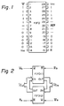
- First, the prior art bidirectional semiconductor device will be explained with reference to Figs. 1 and 2.
- In Fig. 1, which illustrates a prior art one-directional device, i.e., a FIFO memory, a write control signal
W is fixed to a first pin, input data IN (I0 to I8) is fixed to second to sixth pins and 24-th to 27-th pins, a read control signalR is fixed to a 15-th pin, and output data OUT (O0 to O8) is fixed to 9-th to 13-th pins and 16-th to 19-th pins. Note that VCC and VSS designate power supplies, and other terminals are designated "Full", "Empty" and the like. - If one-directional FIFO's having the fixed input/ output pins are used for bidirectional data transmission, two FIFO's are connected as illustrated in Fig. 2. As a result, an FIFO (1) is used for data transmission from A-side to B-side, and an FIFO (2) is used for data transmission from B-side to A-side.
- However, when a bidirectional device is constructed as illustrated in Fig. 2, the number of chips on a printed circuit board is increased to increase the board occupied area, and in addition, the input/output (I/O) connections on the printed board become complex. The complexity of the I/O connections also increases the mounting density of the printed board, because of the area occupied thereby, and deteriorates the electrical characteristics due to the stray capacity of the connections.
- In Fig. 3, which illustrates a first embodiment of the present invention, a one-directional internal circuit has an internal input port IN and an internal output port OUT. The internal input port IN is connectable to either an A-side external input/output terminal I/O (A) or a B-side external input/output terminal I/O (B). The same holds true for the internal output port OUT. The switching of such connections is carried out by a switching means, so that the internal input port IN is connected to one of the external ports I/O (A) and I/O (B), and the internal output port OUT is connected to the other external port.
- Also, referring to Fig. 4, which is a detailed circuit diagram of Fig. 3, a frame indicated by a dotted-solid line designates one chip. In this chip, only one FIFO memory is provided as the one-directional internal circuit. At the FIFO memory, internal ports such as a write control port
W , a read control portR , an input port IN, an output port OUT, and a reset portRSTi are provided. Also provided in the periphery of the chip, are A-side external ports such as a write/read control portW/R (A) and an input/output port I/O (A), and B-side external ports such as a write/read control portW/R (B), an input/output port I/O (B), and a reset port RST for the connections to the exterior. The external reset port RST is fixed to the internal reset portRSTi . Further, a first switch SW₁ is provided between the external portsW/R (A), W/R (B) and the internal portW ; a second switch SW₂ is provided between the external portsW/R (A), W/R (B) and the internal portR ; a third switch SW₃ is provided between the external ports I/O (A), I/O (B) and the internal port IN; and a fourth switch SW₄ is provided between the external ports I/O (A), I/O (B) and the internal port OUT. These switches SW₁ to SW₄ are operated simultaneously by a mode signal M supplied from the exterior of the chip. - Note that the internal ports IN and OUT, and the external ports I/O (A) and I/O (B) of Fig. 4, actually have a multi-bit configuration such as a 9-bit configuration as illustrated in Fig. 1, but, for simplification, such ports have a single-bit configuration in Fig. 4.
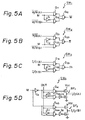
- Each of the switches SW₁ to SW₄ of Fig. 4 will be explained with reference to Figs. 5A to 5D.
- As illustrated in Fig. 5A, the switch SW₁ is comprised of NAND circuits G₁₁ , G₁₂ , and G₁₃ , and an inverter I₁. Therefore, when the mode signal M is "1", the signal at the external control port
W/R (A) is supplied to the write control portW of the FIFO memory, and when the mode signal M is "0", the signal at the external control portW/R (B) is supplied to the write control portW of the FIFO memory. - Similarly, as illustrated in Fig. 5B, the switch SW₂ is comprised of NAND circuits G₂₁ , G₂₂ , and G₂₃ , and an inverter I₂. Therefore, when the mode signal M is "1", the signal at the external control port
W/R (B) is supplied to the write control portW of the FIFO memory, and when the mode signal M is "0", the signal at the external control portW/R (A) is supplied to the write control portW of the FIFO memory. - Also, as illustrated in Fig. 5C, the switch SW₃ is comprised of NAND circuits G₃₁ , G₃₂ , and G₃₃ , and an inverter I₃. Therefore, when the mode signal M is "1", the signal at the external port I/O (A) is supplied to the input data port IN of the FIFO memory, and when the mode signal M is "0", the signal at the external port I/O (E) is supplied to the input data port IN of the FIFO memory.
- Further, as illustrated in Fig. 5D, the switch SW₄ is comprised of NAND circuits G₄₁ , G₄₂ , G₄₃ , and G₄₄ , inverters I₄ to I₈ and CMOS buffers BF₁ and BF₂. Therefore, when the mode signal M is "1", the lower-side circuit of Fig. 5D is operated so that data at the output data port OUT is transmitted to the B-side port I/O (B), and when the mode signal M is "0", the upper-side circuit of Fig. 5D is operated so that data at the output data port OUT is transmitted to the A-side port I/O (A).
- Thus, in summary, the following table is obtained.
M = "1" M = "0" W W/R (A)W/R (B)R W/R (B)W/R (A)IN I/O (A) I/O (B) OUT I/O (B) I/O (A) - In Fig. 6, which is a detailed circuit diagram of the FIFO memory of Fig. 4, a static memory cell MCij is provided between a write word line WLi (W), and a read word line WLi (R), and in write bit lines BLj (W),
BLj (W) and read bit lines BLj (R),BLj (R). In a write mode (W = "0"), write data IN is written by a write amplifier WA into the memory cell MCij between a word line such as WLi (W) selected by a write pointer WP (1) and write bit lines such as BLj (W),BLj (W) selected by a write pointer WP (2). On the other hand, in a read mode (R = "0"), data of a memory cell between a read word line such as WLi (R) selected by a read pointer RP (1) and read bit lines such as BLj (R),BLj (R) selected by a read pointer RP (2) is read and is transmitted as output data OUT via a read amplifier RA. - In a write operation of the FIFO memory, as illustrated in Figs. 7A to 7D, the write pointers WP (1) and WP (2) are counted up one by one in accordance with a write control signal
W , thereby sequentially accessing the memory cells and writing data thereinto. Note that, in this case, the two write pointers serve as one write pointer WP and are reset by a reset signalRST . That is, every time one of the write pointers WP (1) and WP (2) is cycled, the other pointer is counted up by +1. - On the other hand, in a read operation of the FIFO memory, as illustrated in Figs. 7A, and 7E to 7G, the read pointers RP (1) and RP (2) are counted up one by one in accordance with a read control signal
R , thereby sequentially accessing the memory cells and reading data therefrom. Note that, also in this case, the two read pointers serve as one read pointer RP and are reset by a reset signalRST . That is, every time one of the read pointers RP (1) and RP (2) is cycled, the other pointer is counted up by +1. - In Fig. 8, which illustrates a second embodiment of the present invention, a mode setting circuit SC for generating the mode signal M is added to the elements of the first embodiment of Fig. 4. The mode setting circuit SC detects the presence or absence of an overlap at a predetermined level such as "0" level of the signals of at least two originally existing external ports such as RST and
W/R (B) without additional special ports, thereby generating the mode signal M within the chip. - The mode setting circuit SC of Fig. 8 will be explained with reference to Fig. 9. The mode setting circuit SC is comprised of an overlap detector (NOR circuit) DET1 for detecting an overlap of a low level ("0") of the external reset signal
RST and a low level of an external write/read control signal R/W (B), a fall detector DET2 comprised of a delay circuit DL, an inverter I¹ , and a NOR circuit G₂ , and an RS flip-flop FF serving as a memory. This RS flip-flop FF is constructed as shown in Fig. 10. In the RS flip-flop FF, a power supply VCC is applied to a set terminal S, a ground potential is applied to a reset terminal R, the output of the overlap detector DET1 is applied to a clock terminal CK, and the output of the fall detector DET2 is applied to a clear terminal CL. - Therefore, as illustrated in Figs. 11A through 11E, after the FIFO memory is reset by the signal
RST and the flip-flop FF is reset by the output of the fall detector DET2 (RST = "0"), even when the signal of the external control portW/R (B) is changed after the sufficient recovery of the reset signalRST , the output of the overlap detector DET1 remains at "0". As a result, the flip-flop FF remains in a reset state, and therefore, the mode signal M remains at "1". On the other hand, as illustrated in Figs. 12A through 12E, after the FIFO memory is reset by the reset signal RST and the flip-flop FF is reset by the output of the fall detector DET2 (RST = "0"), when the signal of the external control portW/R (B) is changed before the recovery of the reset signalRST , the overlap detector DET1 detects an overlap of a low level betweenRST andW/R (B) to change the output thereof from "0" to "1". As a result, the flip-flop FF is set so that the mode signal M becomes "0". Thus, a desired mode signal M is generated within the chip by the inputs of the originally existing external ports without adding special external ports. - Note that, in Fig. 9, the flip-flop FF is reset (cleared) by the reset signal
RST , but such a reset operation can be carried out by applying the power supply if the circuit constants of the flip-flop FF are suitably set. Also, as occasion demands, the detector DET1 may detect an overlap of a high level between the two external ports, and a rise detector may be used instead of the fall detector DET2. Further, the mode signal M is set by an overlap of the signals of the two external input signalsRST ,W/R (B), but other external input signals can be used. - In Fig. 13, which illustrates a third embodiment of the present invention, a mode setting circuit SC' for generating the mode signal M is added to the elements of the first embodiment of Fig. 4. The mode setting circuit SC' detects the sequence of the signals of at least two originally existing external ports such as W/R (A) and W/R (B) without additional special ports, thereby generating the mode signal M within the chip.
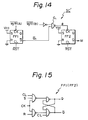
- The mode setting circuit SC' of Fig. 13 will be explained with reference to Fig. 14. The mode setting circuit SC' is comprised of two RS flip-flops FF1 and FF2 each of which is constructed as shown in Fig. 15. In the RS flip-flop FF1, a power supply VCC is applied to a set terminal S, a ground potential is applied to a reset terminal R, the reset signal RST is applied to a clear terminal CL, and the signal at the A-side external input/output control port
W/R (A) is applied to a clock terminal CK. In addition, the output

RST is applied to a clear terminal CL, and the signal φ is applied to a clock terminal CK. Then, the outputQ of the flip-flop FF2 serves as the mode signal M. - Therefore, as illustrated in Figs. 16A through 16F, after the FIFO memory is reset by the reset signal
RST (RST = "0"), when the pulse of the A-side input/output control portW/R (A) precedes the pulse of the B-side input/output control portW/R (B), the mode signal M remains at "1". On the other hand, as illustrated in Figs. 17A through 17F, after the FIFO memory is reset by the reset signalRST (RST = "0"), when the pulse of the B-side input/output control portW/R (B) precedes the pulse of the A-side input/output control portW/R (A), the mode signal M becomes a low level ("0"). Thus, a desired mode signal M is generated within the chip by the inputs of the originally existing external ports without adding special external ports. - Note that, in Fig. 14, the flip-flops FF1 and FF2 are reset (cleared) by the reset signal
RST , but such a reset operation can be carried out by applying the power supply if the circuit constants of the flip-flops FF1 and FF2 are suitably set. Also, in this case, the mode signal M is determined by which of the A-side input/ output control portW/R (A) and the B-side input/output control portW/R (B) receives a preceding pulse. Further, in the circuit of Fig. 14, it is particularly useful in the FIFO memory to determine which of the portsW/R (A) andW/R (B) is a write-side to which a preceding pulse is applied. That is, in the FIFO memory, after resetting, there is no purpose to a read if there is no written data, and accordingly, a write instruction commonly precedes a read instruction. - Note that, in the above-mentioned embodiments, an FIFO memory is used as a one-directional circuit, however, the present invention can be applied to other circuits such as LIFO and a shift register.
- As explained above, according to the present invention, since the bidirectional semiconductor device is constructed by only one one-directional circuit, the board occupied area on a printed circuit board can be reduced, and in addition, the connections thereof can be simplified.
Claims (5)
- A bidirectional semiconductor device comprising:
only one one-directional internal circuit having an internal input port (IN) and an internal output port (OUT);
first and second external input/output ports (I/O(A), I/O (B)); and,
switching means (SW) for connecting the internal input port to one of the first or second external input/output ports and connecting the internal output port to the other of the first and second external input/output ports in accordance with a mode signal (M) generated by a mode signal generating means, characterised in that the onedirectional internal circuit further has a plurality of internal control ports (W, R, RSTi), in that the device further comprises a plurality of external control ports (W/R (A),W/R (B),RST ) connectable to the internal control ports, in that the mode signal generating means (SC) is connected to one of the external control ports, in that the switching means also connects the internal control ports to the external control ports in accordance with the mode signal, and in that the mode signal generating means (SC) controls the switching means in accordance with a sequence between at least two of said external control ports after an application of a power supply or after an initial set. - A device as set forth in claim 1, wherein the mode signal generating means (SC') comprises:
a first flip-flop (FF1), connected to first and second ports (RST ,W/R (A)) of the external control ports, for detecting a change at the signal of the second port after a signal at the first port is changed;
a gate (G₁), connected to a third port (W/R (B)) of the external control ports and to the output of the first flip-flop, for passing a signal at the third port through it in accordance with an output of the first flip-flop and,
a second flip-flop (FF2), connected to the first external control port and to an output of the gate, the second flip-flop being reset by a signal at the first port and set by an output of the gate, thereby generating the mode signal. - A device as set forth in any one of the preceding claims, wherein the one-directional internal circuit comprises a first-in first-out memory (FIFO).
- A device as set forth in any of the preceding claims, wherein the one-directional internal circuit comprises a last-in first-out memory (LIFO).
- A device as set forth in any of the preceding claims, wherein the one-directional internal circuit comprises a shift register.
Applications Claiming Priority (6)
| Application Number | Priority Date | Filing Date | Title |
|---|---|---|---|
| JP61298887A JPS63152083A (en) | 1986-12-17 | 1986-12-17 | Bidirectional semiconductor device |
| JP298895/86 | 1986-12-17 | ||
| JP298887/86 | 1986-12-17 | ||
| JP61298895A JPS63152084A (en) | 1986-12-17 | 1986-12-17 | Two-way directional semiconductor device |
| JP61300112A JPS63153787A (en) | 1986-12-18 | 1986-12-18 | Two-way semiconductor device |
| JP300112/86 | 1986-12-18 |
Publications (3)
| Publication Number | Publication Date |
|---|---|
| EP0272847A2 EP0272847A2 (en) | 1988-06-29 |
| EP0272847A3 EP0272847A3 (en) | 1990-03-28 |
| EP0272847B1 true EP0272847B1 (en) | 1994-06-22 |
Family
ID=27338257
Family Applications (1)
| Application Number | Title | Priority Date | Filing Date |
|---|---|---|---|
| EP87310861A Expired - Lifetime EP0272847B1 (en) | 1986-12-17 | 1987-12-10 | Bidirectional semiconductor device having only one one-directional device |
Country Status (4)
| Country | Link |
|---|---|
| US (1) | US4825098A (en) |
| EP (1) | EP0272847B1 (en) |
| KR (1) | KR910000153B1 (en) |
| DE (1) | DE3750124D1 (en) |
Families Citing this family (11)
| Publication number | Priority date | Publication date | Assignee | Title |
|---|---|---|---|---|
| US4894558A (en) * | 1988-10-11 | 1990-01-16 | Nec Electronics Inc. | Power saving input buffer for use with a gate array |
| US4906870A (en) * | 1988-10-31 | 1990-03-06 | Atmel Corporation | Low power logic array device |
| US5235543A (en) * | 1989-12-29 | 1993-08-10 | Intel Corporation | Dual port static memory with one cycle read-modify-write |
| US5384730A (en) * | 1991-05-31 | 1995-01-24 | Thunderbird Technologies, Inc. | Coincident activation of pass transistors in a random access memory |
| JPH05151778A (en) * | 1991-06-05 | 1993-06-18 | Mitsubishi Electric Corp | Static randum access memory and its control method |
| US5216295A (en) * | 1991-08-30 | 1993-06-01 | General Instrument Corp. | Current mode logic circuits employing IGFETS |
| US5381528A (en) * | 1992-10-15 | 1995-01-10 | Maxtor Corporation | Demand allocation of read/write buffer partitions favoring sequential read cache |
| KR0140179B1 (en) * | 1994-12-19 | 1998-07-15 | 김광호 | Nonvolatile semiconductor memory |
| JPH1073643A (en) * | 1996-09-02 | 1998-03-17 | Mitsubishi Electric Corp | Semiconductor device testing jig |
| US6029253A (en) * | 1997-10-30 | 2000-02-22 | Micron Electronics, Inc. | Method for synchronizing data with a bi-directional buffer |
| US6055597A (en) * | 1997-10-30 | 2000-04-25 | Micron Electronics, Inc. | Bi-directional synchronizing buffer system |
Family Cites Families (7)
| Publication number | Priority date | Publication date | Assignee | Title |
|---|---|---|---|---|
| JPS5247636A (en) * | 1975-10-15 | 1977-04-15 | Toshiba Corp | Control method for transmitting information |
| US4344132A (en) * | 1979-12-14 | 1982-08-10 | International Business Machines Corporation | Serial storage interface apparatus for coupling a serial storage mechanism to a data processor input/output bus |
| US4481623A (en) * | 1982-11-23 | 1984-11-06 | Burroughs Corporation | Speed independent arbiter switch employing M-out-of-N codes |
| US4621201A (en) * | 1984-03-30 | 1986-11-04 | Trilogy Systems Corporation | Integrated circuit redundancy and method for achieving high-yield production |
| JPS6188538A (en) * | 1984-10-05 | 1986-05-06 | Fujitsu Ltd | Semiconductor device |
| JPS61263313A (en) * | 1985-05-17 | 1986-11-21 | Matsushita Electric Ind Co Ltd | Latch circuit with selector |
| US4774422A (en) * | 1987-05-01 | 1988-09-27 | Digital Equipment Corporation | High speed low pin count bus interface |
-
1987
- 1987-12-08 US US07/130,630 patent/US4825098A/en not_active Expired - Lifetime
- 1987-12-10 EP EP87310861A patent/EP0272847B1/en not_active Expired - Lifetime
- 1987-12-10 DE DE3750124T patent/DE3750124D1/en not_active Expired - Lifetime
- 1987-12-17 KR KR8714385A patent/KR910000153B1/en not_active IP Right Cessation
Also Published As
| Publication number | Publication date |
|---|---|
| KR880008338A (en) | 1988-08-30 |
| KR910000153B1 (en) | 1991-01-21 |
| EP0272847A3 (en) | 1990-03-28 |
| EP0272847A2 (en) | 1988-06-29 |
| US4825098A (en) | 1989-04-25 |
| DE3750124D1 (en) | 1994-07-28 |
Similar Documents
| Publication | Publication Date | Title |
|---|---|---|
| US5818350A (en) | High performance method of and system for selecting one of a plurality of IC chip while requiring minimal select lines | |
| US6519674B1 (en) | Configuration bits layout | |
| US4535427A (en) | Control of serial memory | |
| EP0272847B1 (en) | Bidirectional semiconductor device having only one one-directional device | |
| US4884192A (en) | Information processor capable of data transfer among plural digital data processing units by using an active transmission line having locally controlled storage of data | |
| KR100902765B1 (en) | First-in, first-out memory system and method thereof | |
| US4969126A (en) | Semiconductor memory device having serial addressing and operating method thereof | |
| KR900000048B1 (en) | The lsi memory circuit | |
| EP0398816B1 (en) | Testing method, testing circuit and semiconductor integrated circuit having testing circuit | |
| EP0401521A2 (en) | Semiconductor memory device | |
| EP0444825A2 (en) | Register circuit for scan pass | |
| EP0145497A2 (en) | Semiconductor integrated circuit device | |
| EP0496391B1 (en) | Semiconductor memory device | |
| EP0012017A2 (en) | Programmable computer comprising means for checking the error-correcting circuits | |
| GB2276744A (en) | Memory module with parity bit emulation. | |
| EP0204130B1 (en) | Apparatus for reducing test data storage requirements for high speed vlsi circuit testing | |
| US5285415A (en) | Data counting memory card and reader | |
| US4922457A (en) | Serial access memory system provided with improved cascade buffer circuit | |
| EP1074991B1 (en) | Semiconductor memory device | |
| US4205301A (en) | Error detecting system for integrated circuit | |
| US5117395A (en) | Expansible FIFO memory for accommodating added memory stages in a multistage memory with common control signals | |
| US5426432A (en) | IC card | |
| US20020133664A1 (en) | Cache memory | |
| US6998873B2 (en) | Data input/output buffer and semiconductor memory device using the same | |
| US6222793B1 (en) | Memory devices having a restore start address counter |
Legal Events
| Date | Code | Title | Description |
|---|---|---|---|
| PUAI | Public reference made under article 153(3) epc to a published international application that has entered the european phase |
Free format text: ORIGINAL CODE: 0009012 |
|
| AK | Designated contracting states |
Kind code of ref document: A2 Designated state(s): DE FR GB |
|
| PUAL | Search report despatched |
Free format text: ORIGINAL CODE: 0009013 |
|
| AK | Designated contracting states |
Kind code of ref document: A3 Designated state(s): DE FR GB |
|
| 17P | Request for examination filed |
Effective date: 19900921 |
|
| 17Q | First examination report despatched |
Effective date: 19921125 |
|
| GRAA | (expected) grant |
Free format text: ORIGINAL CODE: 0009210 |
|
| AK | Designated contracting states |
Kind code of ref document: B1 Designated state(s): DE FR GB |
|
| REF | Corresponds to: |
Ref document number: 3750124 Country of ref document: DE Date of ref document: 19940728 |
|
| PG25 | Lapsed in a contracting state [announced via postgrant information from national office to epo] |
Ref country code: DE Effective date: 19940923 |
|
| ET | Fr: translation filed | ||
| PGFP | Annual fee paid to national office [announced via postgrant information from national office to epo] |
Ref country code: GB Payment date: 19941130 Year of fee payment: 8 |
|
| PLBE | No opposition filed within time limit |
Free format text: ORIGINAL CODE: 0009261 |
|
| STAA | Information on the status of an ep patent application or granted ep patent |
Free format text: STATUS: NO OPPOSITION FILED WITHIN TIME LIMIT |
|
| 26N | No opposition filed | ||
| PG25 | Lapsed in a contracting state [announced via postgrant information from national office to epo] |
Ref country code: GB Effective date: 19951210 |
|
| GBPC | Gb: european patent ceased through non-payment of renewal fee |
Effective date: 19951210 |
|
| PGFP | Annual fee paid to national office [announced via postgrant information from national office to epo] |
Ref country code: FR Payment date: 20031210 Year of fee payment: 17 |
|
| PG25 | Lapsed in a contracting state [announced via postgrant information from national office to epo] |
Ref country code: FR Free format text: LAPSE BECAUSE OF NON-PAYMENT OF DUE FEES Effective date: 20050831 |
|
| REG | Reference to a national code |
Ref country code: FR Ref legal event code: ST |