EP0306021A2 - Chip mounting apparatus - Google Patents
Chip mounting apparatus Download PDFInfo
- Publication number
- EP0306021A2 EP0306021A2 EP88114280A EP88114280A EP0306021A2 EP 0306021 A2 EP0306021 A2 EP 0306021A2 EP 88114280 A EP88114280 A EP 88114280A EP 88114280 A EP88114280 A EP 88114280A EP 0306021 A2 EP0306021 A2 EP 0306021A2
- Authority
- EP
- European Patent Office
- Prior art keywords
- tray
- chips
- concaves
- mounting apparatus
- chip
- Prior art date
- Legal status (The legal status is an assumption and is not a legal conclusion. Google has not performed a legal analysis and makes no representation as to the accuracy of the status listed.)
- Granted
Links
Images


Classifications
-
- H—ELECTRICITY
- H05—ELECTRIC TECHNIQUES NOT OTHERWISE PROVIDED FOR
- H05K—PRINTED CIRCUITS; CASINGS OR CONSTRUCTIONAL DETAILS OF ELECTRIC APPARATUS; MANUFACTURE OF ASSEMBLAGES OF ELECTRICAL COMPONENTS
- H05K13/00—Apparatus or processes specially adapted for manufacturing or adjusting assemblages of electric components
- H05K13/04—Mounting of components, e.g. of leadless components
- H05K13/0404—Pick-and-place heads or apparatus, e.g. with jaws
- H05K13/0413—Pick-and-place heads or apparatus, e.g. with jaws with orientation of the component while holding it; Drive mechanisms for gripping tools, e.g. lifting, lowering or turning of gripping tools
-
- H—ELECTRICITY
- H05—ELECTRIC TECHNIQUES NOT OTHERWISE PROVIDED FOR
- H05K—PRINTED CIRCUITS; CASINGS OR CONSTRUCTIONAL DETAILS OF ELECTRIC APPARATUS; MANUFACTURE OF ASSEMBLAGES OF ELECTRICAL COMPONENTS
- H05K13/00—Apparatus or processes specially adapted for manufacturing or adjusting assemblages of electric components
- H05K13/02—Feeding of components
-
- H—ELECTRICITY
- H05—ELECTRIC TECHNIQUES NOT OTHERWISE PROVIDED FOR
- H05K—PRINTED CIRCUITS; CASINGS OR CONSTRUCTIONAL DETAILS OF ELECTRIC APPARATUS; MANUFACTURE OF ASSEMBLAGES OF ELECTRICAL COMPONENTS
- H05K13/00—Apparatus or processes specially adapted for manufacturing or adjusting assemblages of electric components
- H05K13/08—Monitoring manufacture of assemblages
- H05K13/081—Integration of optical monitoring devices in assembly lines; Processes using optical monitoring devices specially adapted for controlling devices or machines in assembly lines
- H05K13/0815—Controlling of component placement on the substrate during or after manufacturing
-
- H—ELECTRICITY
- H01—ELECTRIC ELEMENTS
- H01L—SEMICONDUCTOR DEVICES NOT COVERED BY CLASS H10
- H01L2221/00—Processes or apparatus adapted for the manufacture or treatment of semiconductor or solid state devices or of parts thereof covered by H01L21/00
- H01L2221/67—Apparatus for handling semiconductor or electric solid state devices during manufacture or treatment thereof; Apparatus for handling wafers during manufacture or treatment of semiconductor or electric solid state devices or components; Apparatus not specifically provided for elsewhere
- H01L2221/683—Apparatus for handling semiconductor or electric solid state devices during manufacture or treatment thereof; Apparatus for handling wafers during manufacture or treatment of semiconductor or electric solid state devices or components; Apparatus not specifically provided for elsewhere for supporting or gripping
- H01L2221/68304—Apparatus for handling semiconductor or electric solid state devices during manufacture or treatment thereof; Apparatus for handling wafers during manufacture or treatment of semiconductor or electric solid state devices or components; Apparatus not specifically provided for elsewhere for supporting or gripping using temporarily an auxiliary support
- H01L2221/68313—Auxiliary support including a cavity for storing a finished device, e.g. IC package, or a partly finished device, e.g. die, during manufacturing or mounting
-
- Y—GENERAL TAGGING OF NEW TECHNOLOGICAL DEVELOPMENTS; GENERAL TAGGING OF CROSS-SECTIONAL TECHNOLOGIES SPANNING OVER SEVERAL SECTIONS OF THE IPC; TECHNICAL SUBJECTS COVERED BY FORMER USPC CROSS-REFERENCE ART COLLECTIONS [XRACs] AND DIGESTS
- Y10—TECHNICAL SUBJECTS COVERED BY FORMER USPC
- Y10T—TECHNICAL SUBJECTS COVERED BY FORMER US CLASSIFICATION
- Y10T29/00—Metal working
- Y10T29/53—Means to assemble or disassemble
- Y10T29/5313—Means to assemble electrical device
- Y10T29/53174—Means to fasten electrical component to wiring board, base, or substrate
- Y10T29/53178—Chip component
-
- Y—GENERAL TAGGING OF NEW TECHNOLOGICAL DEVELOPMENTS; GENERAL TAGGING OF CROSS-SECTIONAL TECHNOLOGIES SPANNING OVER SEVERAL SECTIONS OF THE IPC; TECHNICAL SUBJECTS COVERED BY FORMER USPC CROSS-REFERENCE ART COLLECTIONS [XRACs] AND DIGESTS
- Y10—TECHNICAL SUBJECTS COVERED BY FORMER USPC
- Y10T—TECHNICAL SUBJECTS COVERED BY FORMER US CLASSIFICATION
- Y10T29/00—Metal working
- Y10T29/53—Means to assemble or disassemble
- Y10T29/5313—Means to assemble electrical device
- Y10T29/53261—Means to align and advance work part
Definitions
- the present invention relates to a chip mounting apparatus for sorting and subsequently readily mounting each of a large number of generally square chip components, for example, semiconductor chips, chip capacitors, chip resistors or the like onto a package base or a circuit board.
- a large number of semiconductor elements are initially formed into a certain pattern on a semiconductor wafer and are then individually separated into generally square chips.
- the separated semiconductor chips Prior to subsequent die-bonding process, the separated semiconductor chips are successively transported to a chip mounting apparatus, while being bonded on an adhesive expand tape.
- the semiconductor chips are separated from the expand tape and then picked up one by one by a vacuum pickup collet or the like so as to be mounted on a package base.
- the chips separated from the tape are occasionally placed on a tray to be rearranged in order.
- Fig.1 depicts a tray 1 to be used for this purpose, which is provided at its upper surface with a plurality of generally square concaves 4 partitioned in regular order generally in the form of a checked pattern by a plurality of partition walls 2 and 3 crossing at right angles.
- the concaves 4 have the same configuration slightly greater than any chips so that each of the concaves 4 can accommodate any one of the chips regardless of size.
- the present invention has been developed with a view to substantially eliminating the above described disadvantage inherent in the prior art chip mounting apparatus, and has for its essential object to provide an improved chip mounting apparatus in which a plurality of chips are placed in order on a tray in a fashion such that each of the chips is accommodated in any one of a plurality of concaves formed in the tray in the same positional relationship between the chips and respective concaves.
- Another important object of the present invention is to provide a chip mounting apparatus of the above described type which is capable of readily and speedily picking up the chips accommodated in respective concaves one by one with the use of a vacuum pickup collet.
- a further object of the present invention is to provide a chip mounting apparatus which is stable in functioning and can be readily manufactured at a relatively low cost.
- a chip mounting apparatus is provided with a base, a support member securely held on the base, a tray detachably mounted in the support member and provided with a plurality of substantially square concaves each for accommodating one of the chips, and an oscillating means for oscillating the tray.
- the concaves of the tray are regularly spaced from one another by a plurality of partition walls formed on the tray.
- the support member is capable of inclining the tray so that one corner of each concave may become lower than any other corners thereof.
- the chip mounting apparatus is further provided with a vacuum pickup collet having two projections located diagonally on its lower surface whereas the tray is provided with a plurality of cross-shaped notches at crossings of the partition walls. Accordingly, since there never occurs any interference between the collet and the partition walls of the tray, the collet can reliably and speedily pick up each chip.
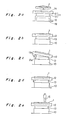
- Figs. 2a to 2e depict a chip mounting apparatus according to one preferred embodiment of the present invention, which is provided with a base 10, a stage 11 securely held on the base 10, a vacuum pickup collet 15 for picking up one by one a plurality of chips placed on a tray 1 and the like.
- the stage 11 is comprised of a tray chuck 12 for securely holding or chucking therein the tray 1 shown in Fig. 1, and a lifter 13 for supporting and inclining the tray chuck 12.
- a hollow 14 is formed at an upper surface of the tray chuck 12 to securely hold therein the tray 1 by drawing the vacuum or by any other suitable holding means, for example, a mechanical chuck by virtue of a flat spring or the like.
- the lifter 13 is so operable as to incline the tray chuck 12 and is, therefore, connected with any suitable driving means (not shown) provided inside it or inside the base 10.
- the lifter 13 consists of an external cylinder 13a and an internal cylinder 13b which is reciprocably and rotatably inserted into the external cylinder 13a. Upon rotation and upward movement of the internal cylinder 13b, the tray chuck 12 is inclined, as shown in Fig. 2c.
- Figs. 3a to 3e show a modification of the chip mounting apparatus, which is provided with a lifter 13 ⁇ comprised of at least two rods, preferably four rods, to incline the tray chuck 12 upon upward movement of any one of the rods.
- the tray 1 is inclined together with the tray chuck 12 in a fashion such that one of the corners of each concave 4 formed in the tray 1 is located lower than any other corners. Because of this, one corner of each chip is positioned in one corner of the concave 4 for proper positioning of the chip.
- the angle of inclination of the tray 1 should be a minute angle, for example, approximately 3 degrees. If the angle of inclination exceeds this value, the chips are always in danger of dropping from the tray 1.
- the chip mounting apparatus of the present invention is further provided with an oscillating means 19 for oscillating the stage 11 or at least the tray chuck 12 thereof to oscillate the tray 1 together therewith.
- the oscillating means 19 may be accommodated in the base 10 of the apparatus or may be provided outside and connected to the base 10 by means of a rod or the like.
- the oscillation having a minute amplitude which never cause the chips to drop from the tray 1 is preferably selected to smoothly slide the chips.
- Such the oscillation is caused by, for example, a supersonic wave oscillating device.
- the tray 1 provided with a plurality of concaves 4 each accommodating one chip is initially transported above and securely chucked in the hollow 14 formed in the tray chuck 12.
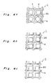
- the chips 20 are located at random at different positions in respective concaves 4, as shown in Fig. 4a.
- the tray chuck 12 is inclined upon operation of the lifter 13 or 13 ⁇ , thereby rendering the tray 1 to be inclined in a fashion such that one corner of each concave 4 is so positioned as to be lower than any other corners, as shown in Fig. 2c or Fig. 3c.
- Subsequent oscillation of the tray 1 by the oscillating means 19 slides the chips 20 accommodated at random in respective concaves 4 of the tray 1 towards the lowered corners of the concaves 4.
- the chips 20 are gradually rearranged in respective concaves 4, as shown in Fig. 4b, and are finally positioned in the lowered corners thereof in order so that one corner of each chip 20 may be in accord with the lowered corner of one concave 4, as shown in Fig. 4c. In this way, all of the chips 20 are brought into contact with the same corners of respective concaves 4 and properly positioned therein.
- the lifter 13 or 13 ⁇ is restored to its rest position shown in Fig. 2d or Fig. 3d so that the chips 20 may be picked up one by one by the collet 15, as shown in Fig. 2e or Fig. 3e.
- the collet 15 is movable in any desired direction to pick up each chip 20 by drawing the vacuum therethrough. During the pickup, since all the chips 20 are properly positioned in respective concaves 4, the collet 15 never fails to pick up each of them.
- a direction identification mark 21 may be marked on each chip 20 in advance, as shown in Figs. 5a, 5b and 6a, 6b. Such a mark is formed in the vicinity of one corner of the chip 20, for example, at a location where no circuit pattern is formed.
- the direction of the chip 20 with respect to the tray 1 can be detected through the pattern recognition of the direction identification mark 21.
- the direction identification mark 21 can be formed by applying ink onto the chip 20 through an ink jet or by forming a desired pattern thereon when the circuit pattern is formed.
- Figs. 6a and 6b depict a manufacturing process in the case where the chips 20 are semiconductor chips.
- a plurality of direction identification marks 21 are formed on the same corners of respective chips 20 bonded on a semiconductor wafer 23, as shown in Fig. 6a. Some of the chips of poor quality are also marked each with a quality poor mark 24.
- the semiconductor wafer 23 is separated into individual chips 20, which are then picked up by any known pickup means, for example, a collet to be accommodated in respective concaves 4 of the tray 1, as shown in Fig. 6b. In this event, the chips 20 with the quality poor mark 24 are sorted when picked up by the collet or the like and never be placed on the tray 1.
- the chips 20 with the direction identification mark 21 are placed and properly positioned on the tray 1 as shown in Fig. 5b, upon oscillation thereof in the above described manner.
- Fig. 7 depicts a portion of a tray 1a according to the present invention in which a plurality of cross-shaped notches 24 are formed at all crossings of partition walls 2a and 3a. The reason for this is to prevent the interference between the collet 15 and the partition walls 2a and 3a during the pickup of the chips 20.
- Fig. 7 illustrates the tray 1a provided with the notches 24 formed at all the four corners of the concaves 4, at least two notches may be formed respectively at two corners positioned diagonally with respect to one concave 4.
- a plurality of spaced rectangular parallelepipeds 2b and 3b may be bonded on the tray 1b in a fashion such that a plurality of substantially square concaves 4b are regularly spaced from one another and are each defined by four rectangular parallelepipeds 2b and 3b.
- the vacuum pickup collet 15 for picking up the chips 20 placed on the tray 1 is of a configuration as shown in Fig. 9. More specifically, the collet 15 is provided with a suction port 17 for picking up each chip 20 by drawing the vacuum therethrough and is connected with a lower end of a suction pipe 16 which is further connected with any known suction means (not shown), for example, a vacuum pump. When the collet 15 picks up each chip 20, it is brought into contact with peripheral edges of the chip 20 to attract it. To this end, two substantially L-shaped projections 18 are integrally formed with or securely connected to the lower surface of the collet 15 respectively at its diagonally positioned two corners.
- the collet 15 having the above described construction is initially rotated, prior to the downward movement thereof, so that one of the two projections 18 may be in accord with one notch 24 of a certain concave 4. Accordingly, the two projections 18 are brought into contact with the two diagonal corners of the chip 20 in a state in which one of the projections 18 is inserted into the notch 24 whereas the other projection 18 is inserted into the concave 4. In this event, since the lower surface of the collet 15 except its two corners with projections 18 is formed flat, there never occurs the interference between the collet 15 and the partition walls 2a and 3a, thereby ensuring reliable pickup of the chips 20 by the vacuum attraction.
- the chips 20 accommodated in respective concaves 4 at random slides towards the same corners of the concaves 4 and are properly positioned therein upon oscillation of the tray 1 caused by the oscillating means 19.
- the lifter 13 or 13′ is restored to its rest position as shown in Fig. 2d or Fig. 3d so that the chips 20 may be readily picked up by the collet 15 one by one.
- the collet 15 since all the chips 20 are kept in contact with the same corners of respective concaves 4, the collet 15 never fails to pick them up.
- the projections 18 of the collet 15 are reliably brought into contact with the corners of the chip 20, since there is no interference between the collet 20 and the partition walls 2a and 3a. Accordingly, the collet 15 can correctly and speedily pick up the chip 20 by drawing the vacuum therethrough.
Abstract
Description
- The present invention relates to a chip mounting apparatus for sorting and subsequently readily mounting each of a large number of generally square chip components, for example, semiconductor chips, chip capacitors, chip resistors or the like onto a package base or a circuit board.
- In general, a large number of semiconductor elements are initially formed into a certain pattern on a semiconductor wafer and are then individually separated into generally square chips. Prior to subsequent die-bonding process, the separated semiconductor chips are successively transported to a chip mounting apparatus, while being bonded on an adhesive expand tape. During the die-bonding process, the semiconductor chips are separated from the expand tape and then picked up one by one by a vacuum pickup collet or the like so as to be mounted on a package base. Alternatively, the chips separated from the tape are occasionally placed on a tray to be rearranged in order.
- Fig.1 depicts a
tray 1 to be used for this purpose, which is provided at its upper surface with a plurality of generally square concaves 4 partitioned in regular order generally in the form of a checked pattern by a plurality ofpartition walls concaves 4 have the same configuration slightly greater than any chips so that each of theconcaves 4 can accommodate any one of the chips regardless of size. - However, when the chips are placed on such a
tray 1, they are located at different positions or angles insiderespective concaves 4 as a rule, resulting in variations in positional relationship between the chips and the concaves 4 accommodating respective chips. Consequently, the vacuum pickup collet or the like occasionally fails to properly pick up the chips from the tray according to their locations, rendering some of such chips to drop from the collet or to be damaged at their corners. This problem necessitates an image processing system for identifying the position of the chips on thetray 1, which slows each pickup and causes the apparatus to become complicated or to be formed into a relatively large size. - Accordingly, the present invention has been developed with a view to substantially eliminating the above described disadvantage inherent in the prior art chip mounting apparatus, and has for its essential object to provide an improved chip mounting apparatus in which a plurality of chips are placed in order on a tray in a fashion such that each of the chips is accommodated in any one of a plurality of concaves formed in the tray in the same positional relationship between the chips and respective concaves.
- Another important object of the present invention is to provide a chip mounting apparatus of the above described type which is capable of readily and speedily picking up the chips accommodated in respective concaves one by one with the use of a vacuum pickup collet.
- A further object of the present invention is to provide a chip mounting apparatus which is stable in functioning and can be readily manufactured at a relatively low cost.
- In accomplishing these and other objects, a chip mounting apparatus according to one preferred embodiment of the present invention is provided with a base, a support member securely held on the base, a tray detachably mounted in the support member and provided with a plurality of substantially square concaves each for accommodating one of the chips, and an oscillating means for oscillating the tray. The concaves of the tray are regularly spaced from one another by a plurality of partition walls formed on the tray. The support member is capable of inclining the tray so that one corner of each concave may become lower than any other corners thereof. The chip mounting apparatus having the above described construction makes it possible to rearrange the chips in order in the same corners of respective concaves.
- Moreover, since a direction identification mark is formed on one corner of each chip, all of the chips can be directed in the same direction upon recognition of the direction identification mark when being picked up from the tray. This facilitates subsequent processing.
- The chip mounting apparatus according to the present invention is further provided with a vacuum pickup collet having two projections located diagonally on its lower surface whereas the tray is provided with a plurality of cross-shaped notches at crossings of the partition walls. Accordingly, since there never occurs any interference between the collet and the partition walls of the tray, the collet can reliably and speedily pick up each chip.
- These and other objects and features of the present invention will become more apparent from the following description taken in conjunction with the preferred embodiment thereof with reference to the accompanying drawings, throughout which like parts are designated by like reference numerals, and in which:
- Fig.1 is a perspective view of a conventional tray having therein a plurality concaves each for accommodating one chip;
- Figs. 2a to 2e are side elevational views indicative of the construction and the operation of a chip mounting apparatus according to one preferred embodiment of the present invention;
- Figs. 3a to 3e are views similar to Figs. 2a to 2e, which particularly shows a modification thereof;
- Figs. 4a to 4c are top plan views of a portion of the tray, indicative of the way how a plurality of chips accommodated in respective concaves are rearranged in order;
- Figs. 5a and 5b are top plan views of a portion of the tray, indicative of the way how a plurality of chips accommodated in respective concaves and each having thereon a direction identification mark are rearranged in order;
- Figs. 6a and 6b are top plan views of a plurality of semiconductor chips bonded on a semiconductor wafer, indicative of a manufacturing process thereof;
- Fig. 7 is a fragmentary perspective view of a portion of the tray according to the present invention;
- Fig. 8 is a view similar to Fig. 7, which particularly shows a modification thereof; and
- Fig. 9 is a perspective view of a vacuum pickup collet for picking up the chips one by one according to the present invention.
- Figs. 2a to 2e depict a chip mounting apparatus according to one preferred embodiment of the present invention, which is provided with a
base 10, astage 11 securely held on thebase 10, avacuum pickup collet 15 for picking up one by one a plurality of chips placed on atray 1 and the like. Thestage 11 is comprised of atray chuck 12 for securely holding or chucking therein thetray 1 shown in Fig. 1, and alifter 13 for supporting and inclining thetray chuck 12. A hollow 14 is formed at an upper surface of thetray chuck 12 to securely hold therein thetray 1 by drawing the vacuum or by any other suitable holding means, for example, a mechanical chuck by virtue of a flat spring or the like. - The
lifter 13 is so operable as to incline thetray chuck 12 and is, therefore, connected with any suitable driving means (not shown) provided inside it or inside thebase 10. Thelifter 13 consists of anexternal cylinder 13a and aninternal cylinder 13b which is reciprocably and rotatably inserted into theexternal cylinder 13a. Upon rotation and upward movement of theinternal cylinder 13b, thetray chuck 12 is inclined, as shown in Fig. 2c. - Figs. 3a to 3e show a modification of the chip mounting apparatus, which is provided with a
lifter 13´ comprised of at least two rods, preferably four rods, to incline thetray chuck 12 upon upward movement of any one of the rods. - The
tray 1 is inclined together with thetray chuck 12 in a fashion such that one of the corners of each concave 4 formed in thetray 1 is located lower than any other corners. Because of this, one corner of each chip is positioned in one corner of the concave 4 for proper positioning of the chip. - It is to be noted here that the angle of inclination of the
tray 1 should be a minute angle, for example, approximately 3 degrees. If the angle of inclination exceeds this value, the chips are always in danger of dropping from thetray 1. - The chip mounting apparatus of the present invention is further provided with an oscillating
means 19 for oscillating thestage 11 or at least thetray chuck 12 thereof to oscillate thetray 1 together therewith. The oscillatingmeans 19 may be accommodated in thebase 10 of the apparatus or may be provided outside and connected to thebase 10 by means of a rod or the like. The oscillation having a minute amplitude which never cause the chips to drop from thetray 1 is preferably selected to smoothly slide the chips. Such the oscillation is caused by, for example, a supersonic wave oscillating device. - The operation of the chip mounting apparatus having the above described construction will be explained hereinafter.
- As shown in Figs. 2a and 2b or Figs. 3a and 3b, the
tray 1 provided with a plurality ofconcaves 4 each accommodating one chip is initially transported above and securely chucked in thehollow 14 formed in thetray chuck 12. In this event, thechips 20 are located at random at different positions inrespective concaves 4, as shown in Fig. 4a. After the chucking of thetray 1, thetray chuck 12 is inclined upon operation of thelifter tray 1 to be inclined in a fashion such that one corner of each concave 4 is so positioned as to be lower than any other corners, as shown in Fig. 2c or Fig. 3c. - Subsequent oscillation of the
tray 1 by the oscillating means 19 slides thechips 20 accommodated at random inrespective concaves 4 of thetray 1 towards the lowered corners of theconcaves 4. Thechips 20 are gradually rearranged inrespective concaves 4, as shown in Fig. 4b, and are finally positioned in the lowered corners thereof in order so that one corner of eachchip 20 may be in accord with the lowered corner of one concave 4, as shown in Fig. 4c. In this way, all of thechips 20 are brought into contact with the same corners ofrespective concaves 4 and properly positioned therein. - After the positioning of the
chips 20, thelifter chips 20 may be picked up one by one by thecollet 15, as shown in Fig. 2e or Fig. 3e. Thecollet 15 is movable in any desired direction to pick up eachchip 20 by drawing the vacuum therethrough. During the pickup, since all thechips 20 are properly positioned inrespective concaves 4, thecollet 15 never fails to pick up each of them. - If the direction of each
chip 20 is required to be recognized, adirection identification mark 21 may be marked on eachchip 20 in advance, as shown in Figs. 5a, 5b and 6a, 6b. Such a mark is formed in the vicinity of one corner of thechip 20, for example, at a location where no circuit pattern is formed. The direction of thechip 20 with respect to thetray 1 can be detected through the pattern recognition of thedirection identification mark 21. Thedirection identification mark 21 can be formed by applying ink onto thechip 20 through an ink jet or by forming a desired pattern thereon when the circuit pattern is formed. - Figs. 6a and 6b depict a manufacturing process in the case where the
chips 20 are semiconductor chips. - Prior to the dicing, a plurality of direction identification marks 21 are formed on the same corners of
respective chips 20 bonded on asemiconductor wafer 23, as shown in Fig. 6a. Some of the chips of poor quality are also marked each with a qualitypoor mark 24. During the dicing, thesemiconductor wafer 23 is separated intoindividual chips 20, which are then picked up by any known pickup means, for example, a collet to be accommodated inrespective concaves 4 of thetray 1, as shown in Fig. 6b. In this event, thechips 20 with the qualitypoor mark 24 are sorted when picked up by the collet or the like and never be placed on thetray 1. - The
chips 20 with thedirection identification mark 21 are placed and properly positioned on thetray 1 as shown in Fig. 5b, upon oscillation thereof in the above described manner. - When each of the
chips 20 is taken out from thetray 1 by thecollet 15, the direction thereof is recognized by the pattern recognition of itsdirection identification mark 21. In this event, if any of thechips 20 is directed differently fromother chips 20, its direction can be changed by rotating thetray chuck 12 or thecollet 15 according to the position of thedirection identification mark 21. Accordingly, even if one ormore chips 20 are different in direction more than 90 degrees from anyother chips 20, all of thechips 20 can be directed in the same direction when picked up from thetray 1. - Fig. 7 depicts a portion of a tray 1a according to the present invention in which a plurality of
cross-shaped notches 24 are formed at all crossings ofpartition walls collet 15 and thepartition walls chips 20. - It is to be noted that although Fig. 7 illustrates the tray 1a provided with the
notches 24 formed at all the four corners of theconcaves 4, at least two notches may be formed respectively at two corners positioned diagonally with respect to one concave 4. - Alternatively, as shown in Fig. 8, a plurality of spaced
rectangular parallelepipeds rectangular parallelepipeds - In this embodiment, the
vacuum pickup collet 15 for picking up thechips 20 placed on thetray 1 is of a configuration as shown in Fig. 9. More specifically, thecollet 15 is provided with asuction port 17 for picking up eachchip 20 by drawing the vacuum therethrough and is connected with a lower end of asuction pipe 16 which is further connected with any known suction means (not shown), for example, a vacuum pump. When thecollet 15 picks up eachchip 20, it is brought into contact with peripheral edges of thechip 20 to attract it. To this end, two substantially L-shapedprojections 18 are integrally formed with or securely connected to the lower surface of thecollet 15 respectively at its diagonally positioned two corners. - In order to pick up the
chips 20 placed on thetray 1, thecollet 15 having the above described construction is initially rotated, prior to the downward movement thereof, so that one of the twoprojections 18 may be in accord with onenotch 24 of a certain concave 4. Accordingly, the twoprojections 18 are brought into contact with the two diagonal corners of thechip 20 in a state in which one of theprojections 18 is inserted into thenotch 24 whereas theother projection 18 is inserted into the concave 4. In this event, since the lower surface of thecollet 15 except its two corners withprojections 18 is formed flat, there never occurs the interference between thecollet 15 and thepartition walls chips 20 by the vacuum attraction. - In operation, the
chips 20 accommodated inrespective concaves 4 at random slides towards the same corners of theconcaves 4 and are properly positioned therein upon oscillation of thetray 1 caused by the oscillating means 19. - After the positioning of the
chips 20 inrespective concaves 4, thelifter chips 20 may be readily picked up by thecollet 15 one by one. In this event, since all thechips 20 are kept in contact with the same corners ofrespective concaves 4, thecollet 15 never fails to pick them up. When one of thechips 20 is picked up by thecollet 15, theprojections 18 of thecollet 15 are reliably brought into contact with the corners of thechip 20, since there is no interference between thecollet 20 and thepartition walls collet 15 can correctly and speedily pick up thechip 20 by drawing the vacuum therethrough. - Although the present invention has been fully described by way of examples with reference to the accompanying drawings, it is to be noted here that various changes and modifications will be apparent to those skilled in the art. Therefore, unless such changes and modifications otherwise depart from the spirit and scope of the present invention, they should be construed as being included therein.
Claims (3)
a base (10);
a support member (11) securely held on said base (10);
a tray (1; 1a; 1b) detachably mounted in said support member (11) and provided with a plurality of substantially square concaves (4) each for accommodating one of said chips (20), said concaves (4) being regularly spaced from one another by a plurality of partition walls (2, 3; 2a, 3a; 2b, 3b) formed on said tray (1; 1a; 1b), said support member (11) being capable of inclining said tray (1; 1a; 1b) so that one corner of each concave (4) may become lower than any other corners thereof; and
an oscillating means (19) for oscillating said tray (1; 1a; 1b),
whereby said chips (20) are rearranged in order in the same corners of respective concaves (4).
Applications Claiming Priority (6)
| Application Number | Priority Date | Filing Date | Title |
|---|---|---|---|
| JP218553/87 | 1987-09-01 | ||
| JP62218553A JPS6461033A (en) | 1987-09-01 | 1987-09-01 | Device for mounting chip |
| JP62218554A JPH088293B2 (en) | 1987-09-01 | 1987-09-01 | Chip mounting device |
| JP218554/87 | 1987-09-01 | ||
| JP218552/87 | 1987-09-01 | ||
| JP62218552A JPS6461032A (en) | 1987-09-01 | 1987-09-01 | Device for mounting chip |
Publications (3)
| Publication Number | Publication Date |
|---|---|
| EP0306021A2 true EP0306021A2 (en) | 1989-03-08 |
| EP0306021A3 EP0306021A3 (en) | 1990-08-22 |
| EP0306021B1 EP0306021B1 (en) | 1995-01-11 |
Family
ID=27330156
Family Applications (1)
| Application Number | Title | Priority Date | Filing Date |
|---|---|---|---|
| EP88114280A Expired - Lifetime EP0306021B1 (en) | 1987-09-01 | 1988-09-01 | Chip mounting apparatus |
Country Status (5)
| Country | Link |
|---|---|
| US (1) | US4868974A (en) |
| EP (1) | EP0306021B1 (en) |
| AU (1) | AU598393B2 (en) |
| CA (1) | CA1297665C (en) |
| DE (1) | DE3852736T2 (en) |
Cited By (1)
| Publication number | Priority date | Publication date | Assignee | Title |
|---|---|---|---|---|
| EP0576374A1 (en) * | 1992-06-26 | 1993-12-29 | STMicroelectronics S.A. | Tool for mounting a chip between two heat sinks |
Families Citing this family (10)
| Publication number | Priority date | Publication date | Assignee | Title |
|---|---|---|---|---|
| US5207467A (en) * | 1990-08-31 | 1993-05-04 | International Business Machines Corporation | Monitor for detecting the absence of an electronic component on a vacuum pickup |
| US5332463A (en) * | 1992-01-15 | 1994-07-26 | Cray Research, Inc. | Self-aligned sealing fixture for use in assembly of microelectronic packages |
| US6415977B1 (en) * | 2000-08-30 | 2002-07-09 | Micron Technology, Inc. | Method and apparatus for marking and identifying a defective die site |
| JP2003045903A (en) * | 2001-08-01 | 2003-02-14 | Fujitsu Ten Ltd | Die bonding apparatus |
| JP2004111601A (en) * | 2002-09-18 | 2004-04-08 | Tokyo Seimitsu Co Ltd | Die bonder |
| TW546994B (en) * | 2002-10-24 | 2003-08-11 | Htc Corp | Electronic components carrier for collecting electronic components dropping from a circuit board and related method |
| US9214276B2 (en) | 2012-01-16 | 2015-12-15 | Hamilton Sundstrand Corporation | Capacitor |
| KR101787356B1 (en) | 2012-12-25 | 2017-10-19 | 히라따기꼬오 가부시키가이샤 | Transfer system |
| JP6220566B2 (en) * | 2013-06-07 | 2017-10-25 | 株式会社 Synax | Electronic parts transfer device |
| WO2016179023A1 (en) * | 2015-05-01 | 2016-11-10 | Adarza Biosystems, Inc. | Methods and devices for the high-volume production of silicon chips with uniform anti-reflective coatings |
Citations (4)
| Publication number | Priority date | Publication date | Assignee | Title |
|---|---|---|---|---|
| GB2056956A (en) * | 1979-08-30 | 1981-03-25 | Philips Nv | Apparatus for mounting elements on printed circuit board |
| FR2468285A1 (en) * | 1979-10-25 | 1981-04-30 | Hitachi Ltd | METHOD AND APPARATUS FOR MOUNTING PIN-TYPE CIRCUIT CIRCUIT ELEMENTS ON A PRINTED CIRCUIT BOARD |
| JPS582112A (en) * | 1981-06-23 | 1983-01-07 | Hitachi Metals Ltd | Chip aligning device |
| FR2595899A1 (en) * | 1986-03-17 | 1987-09-18 | Nitto Kogyo Kk | METHOD FOR MOUNTING ELECTRONIC COMPONENTS IN SPECIFIED LOCATIONS ON A PRINTED CIRCUIT BOARD |
Family Cites Families (3)
| Publication number | Priority date | Publication date | Assignee | Title |
|---|---|---|---|---|
| FR2446582A1 (en) * | 1979-01-12 | 1980-08-08 | Rech Const Electro Et | POSITIONING OF MICRO-COMPONENTS, ESPECIALLY FOR THICK-LAYER OR THIN-LAYER CIRCUITS |
| US4722135A (en) * | 1986-02-07 | 1988-02-02 | General Electric Co. | Apparatus for placing surface mounting devices on a printer circuit board |
| US4809839A (en) * | 1986-05-16 | 1989-03-07 | Western Digital Corporation | Component handling machine |
-
1988
- 1988-08-29 US US07/237,578 patent/US4868974A/en not_active Expired - Fee Related
- 1988-08-30 CA CA000576092A patent/CA1297665C/en not_active Expired - Fee Related
- 1988-08-31 AU AU21709/88A patent/AU598393B2/en not_active Ceased
- 1988-09-01 DE DE3852736T patent/DE3852736T2/en not_active Expired - Fee Related
- 1988-09-01 EP EP88114280A patent/EP0306021B1/en not_active Expired - Lifetime
Patent Citations (4)
| Publication number | Priority date | Publication date | Assignee | Title |
|---|---|---|---|---|
| GB2056956A (en) * | 1979-08-30 | 1981-03-25 | Philips Nv | Apparatus for mounting elements on printed circuit board |
| FR2468285A1 (en) * | 1979-10-25 | 1981-04-30 | Hitachi Ltd | METHOD AND APPARATUS FOR MOUNTING PIN-TYPE CIRCUIT CIRCUIT ELEMENTS ON A PRINTED CIRCUIT BOARD |
| JPS582112A (en) * | 1981-06-23 | 1983-01-07 | Hitachi Metals Ltd | Chip aligning device |
| FR2595899A1 (en) * | 1986-03-17 | 1987-09-18 | Nitto Kogyo Kk | METHOD FOR MOUNTING ELECTRONIC COMPONENTS IN SPECIFIED LOCATIONS ON A PRINTED CIRCUIT BOARD |
Non-Patent Citations (1)
| Title |
|---|
| PATENT ABSTRACTS OF JAPAN vol. 7, no. 74 (M-203)(1219) 26 March 1983, & JP-A-58 2112 (HITACHI, LTD) 07 January 1983, * |
Cited By (2)
| Publication number | Priority date | Publication date | Assignee | Title |
|---|---|---|---|---|
| EP0576374A1 (en) * | 1992-06-26 | 1993-12-29 | STMicroelectronics S.A. | Tool for mounting a chip between two heat sinks |
| FR2693077A1 (en) * | 1992-06-26 | 1993-12-31 | Sgs Thomson Microelectronics | Chip mounting tool between two heat sinks. |
Also Published As
| Publication number | Publication date |
|---|---|
| DE3852736T2 (en) | 1995-06-14 |
| AU598393B2 (en) | 1990-06-21 |
| EP0306021A3 (en) | 1990-08-22 |
| CA1297665C (en) | 1992-03-24 |
| EP0306021B1 (en) | 1995-01-11 |
| DE3852736D1 (en) | 1995-02-23 |
| AU2170988A (en) | 1989-03-02 |
| US4868974A (en) | 1989-09-26 |
Similar Documents
| Publication | Publication Date | Title |
|---|---|---|
| US6678581B2 (en) | Method of calibrating a wafer edge gripping end effector | |
| US4381601A (en) | Apparatus for mounting electronic components | |
| US4473247A (en) | Component mounting apparatus | |
| US4868974A (en) | Chip mounting apparatus | |
| US4900214A (en) | Method and apparatus for transporting semiconductor wafers | |
| EP0154552A2 (en) | Head and method for orienting electrical components | |
| US6149047A (en) | Die-bonding machine | |
| WO2017130361A1 (en) | Die pickup device | |
| US4910864A (en) | Pick-up head for component handling machine | |
| JP2000077438A (en) | Chip chucking diecollet, chip chucking, chip bonding device and bonding of chip | |
| JP2000117592A (en) | Part mounting device and part feeding device | |
| US4878610A (en) | Die bonding apparatus | |
| JP6734403B2 (en) | Component mounting device | |
| JPH07170094A (en) | Housing tray of electronic-element chip | |
| JPH088293B2 (en) | Chip mounting device | |
| KR920000976Y1 (en) | Chip mounting apparatus | |
| JP2003092313A (en) | Chip inverting device and die-bonder | |
| JP4085730B2 (en) | Electronic component mounting apparatus and electronic component mounting method | |
| TWI732284B (en) | Transfer apparatus and transfer method for transferring light emitting diode chip | |
| JP4449124B2 (en) | Tray support method and apparatus, and tray handling apparatus thereby | |
| JP3006964B2 (en) | Automatic backup pin changer | |
| JPS6342134A (en) | Chip bonding device | |
| JP3514151B2 (en) | Apparatus and method for mounting conductive ball | |
| JPH10256349A (en) | Pickup apparatus | |
| KR100559725B1 (en) | Die bonding apparatus |
Legal Events
| Date | Code | Title | Description |
|---|---|---|---|
| PUAI | Public reference made under article 153(3) epc to a published international application that has entered the european phase |
Free format text: ORIGINAL CODE: 0009012 |
|
| AK | Designated contracting states |
Kind code of ref document: A2 Designated state(s): CH DE FR GB IT LI NL |
|
| PUAL | Search report despatched |
Free format text: ORIGINAL CODE: 0009013 |
|
| AK | Designated contracting states |
Kind code of ref document: A3 Designated state(s): CH DE FR GB IT LI NL |
|
| RHK1 | Main classification (correction) |
Ipc: H05K 13/02 |
|
| 17P | Request for examination filed |
Effective date: 19901030 |
|
| 17Q | First examination report despatched |
Effective date: 19930702 |
|
| GRAA | (expected) grant |
Free format text: ORIGINAL CODE: 0009210 |
|
| AK | Designated contracting states |
Kind code of ref document: B1 Designated state(s): CH DE FR GB IT LI NL |
|
| REF | Corresponds to: |
Ref document number: 3852736 Country of ref document: DE Date of ref document: 19950223 |
|
| ITF | It: translation for a ep patent filed |
Owner name: MODIANO & ASSOCIATI S.R.L. |
|
| ET | Fr: translation filed | ||
| PGFP | Annual fee paid to national office [announced via postgrant information from national office to epo] |
Ref country code: GB Payment date: 19950821 Year of fee payment: 8 |
|
| PGFP | Annual fee paid to national office [announced via postgrant information from national office to epo] |
Ref country code: FR Payment date: 19950911 Year of fee payment: 8 |
|
| PGFP | Annual fee paid to national office [announced via postgrant information from national office to epo] |
Ref country code: CH Payment date: 19950913 Year of fee payment: 8 |
|
| PGFP | Annual fee paid to national office [announced via postgrant information from national office to epo] |
Ref country code: DE Payment date: 19950918 Year of fee payment: 8 |
|
| PGFP | Annual fee paid to national office [announced via postgrant information from national office to epo] |
Ref country code: NL Payment date: 19950922 Year of fee payment: 8 |
|
| PLBE | No opposition filed within time limit |
Free format text: ORIGINAL CODE: 0009261 |
|
| STAA | Information on the status of an ep patent application or granted ep patent |
Free format text: STATUS: NO OPPOSITION FILED WITHIN TIME LIMIT |
|
| 26N | No opposition filed | ||
| ITPR | It: changes in ownership of a european patent |
Owner name: OFFERTA AL PUBBLICO DI LICENZA OFFERTA LICENZA |
|
| REG | Reference to a national code |
Ref country code: GB Ref legal event code: 746 Effective date: 19960319 |
|
| PG25 | Lapsed in a contracting state [announced via postgrant information from national office to epo] |
Ref country code: GB Effective date: 19960901 |
|
| PG25 | Lapsed in a contracting state [announced via postgrant information from national office to epo] |
Ref country code: LI Effective date: 19960930 Ref country code: FR Effective date: 19960930 Ref country code: CH Effective date: 19960930 |
|
| REG | Reference to a national code |
Ref country code: FR Ref legal event code: D9 Free format text: CORRECTION |
|
| PG25 | Lapsed in a contracting state [announced via postgrant information from national office to epo] |
Ref country code: NL Effective date: 19970401 |
|
| GBPC | Gb: european patent ceased through non-payment of renewal fee |
Effective date: 19960901 |
|
| REG | Reference to a national code |
Ref country code: CH Ref legal event code: PL |
|
| NLV4 | Nl: lapsed or anulled due to non-payment of the annual fee |
Effective date: 19970401 |
|
| PG25 | Lapsed in a contracting state [announced via postgrant information from national office to epo] |
Ref country code: DE Effective date: 19970603 |
|
| REG | Reference to a national code |
Ref country code: FR Ref legal event code: ST |
|
| REG | Reference to a national code |
Ref country code: FR Ref legal event code: ST |
|
| PG25 | Lapsed in a contracting state [announced via postgrant information from national office to epo] |
Ref country code: IT Free format text: LAPSE BECAUSE OF NON-PAYMENT OF DUE FEES;WARNING: LAPSES OF ITALIAN PATENTS WITH EFFECTIVE DATE BEFORE 2007 MAY HAVE OCCURRED AT ANY TIME BEFORE 2007. THE CORRECT EFFECTIVE DATE MAY BE DIFFERENT FROM THE ONE RECORDED. Effective date: 20050901 |