EP0320099A2 - Multi-cache data storage system - Google Patents
Multi-cache data storage system Download PDFInfo
- Publication number
- EP0320099A2 EP0320099A2 EP88309704A EP88309704A EP0320099A2 EP 0320099 A2 EP0320099 A2 EP 0320099A2 EP 88309704 A EP88309704 A EP 88309704A EP 88309704 A EP88309704 A EP 88309704A EP 0320099 A2 EP0320099 A2 EP 0320099A2
- Authority
- EP
- European Patent Office
- Prior art keywords
- cache
- physical address
- data
- address
- tag
- Prior art date
- Legal status (The legal status is an assumption and is not a legal conclusion. Google has not performed a legal analysis and makes no representation as to the accuracy of the status listed.)
- Granted
Links
Images

Classifications
-
- G—PHYSICS
- G06—COMPUTING; CALCULATING OR COUNTING
- G06F—ELECTRIC DIGITAL DATA PROCESSING
- G06F12/00—Accessing, addressing or allocating within memory systems or architectures
- G06F12/02—Addressing or allocation; Relocation
- G06F12/08—Addressing or allocation; Relocation in hierarchically structured memory systems, e.g. virtual memory systems
- G06F12/10—Address translation
- G06F12/1027—Address translation using associative or pseudo-associative address translation means, e.g. translation look-aside buffer [TLB]
- G06F12/1045—Address translation using associative or pseudo-associative address translation means, e.g. translation look-aside buffer [TLB] associated with a data cache
- G06F12/1063—Address translation using associative or pseudo-associative address translation means, e.g. translation look-aside buffer [TLB] associated with a data cache the data cache being concurrently virtually addressed
-
- G—PHYSICS
- G06—COMPUTING; CALCULATING OR COUNTING
- G06F—ELECTRIC DIGITAL DATA PROCESSING
- G06F12/00—Accessing, addressing or allocating within memory systems or architectures
- G06F12/02—Addressing or allocation; Relocation
- G06F12/08—Addressing or allocation; Relocation in hierarchically structured memory systems, e.g. virtual memory systems
- G06F12/0802—Addressing of a memory level in which the access to the desired data or data block requires associative addressing means, e.g. caches
- G06F12/0806—Multiuser, multiprocessor or multiprocessing cache systems
- G06F12/0815—Cache consistency protocols
- G06F12/0831—Cache consistency protocols using a bus scheme, e.g. with bus monitoring or watching means
Definitions
- This invention relates to multi-cache data storage systems. More specifically, the invention is concerned with a data storage system of the kind comprising a main store and a plurality of smaller, faster cache stores.
- the invention is particularly although not exclusively concerned with a storage system of this kind for use in a multi-processor data processing system, in which each of the cache stores is associated with a respective one of the processors, and the main store is shared among the processors.
- One way of overcoming this problem is to arrange for each cache to continuously monitor all updates to the main store from any other cache. If any of these updates relate to a data item in the cache, it is updated or invalidated.
- adata storage system using virtual addressing there are two possibilities for addressing the cache store: either with the virtual address or with the corresponding physical (real) address.
- Using the virtual address has the advantage that it does not need to be translated into the physical address before the cache can be accessed, and hence cache access is faster.
- the object of the present invention is to avoid this need to send both the virtual address and the physical address.
- a multi-cache data storage system comprising a plurality of cache units connected by a bus to a main memory, wherein each cache unit comprises:
- the multi-processor system comprises a plurality of processing units 10, and a shared main memory 11.
- Each processing unit 10 has its own cache unit 12.
- the cache units 12 are all connected to the main memory 11 by way of a high speed private memory bus 13.
- a processing unit 10 In operation, when a processing unit 10 requires to read or write a data item, it sends the virtual address VA of that item to its cache unit 12. If the required data item is present in the cache, it can be accessed immediately by the processing unit, for reading or writing. Whenever one of the processors 10 updates a data item in its cache unit 12, the cache generates an update message over the bus to the main memory 11. This ensures that the main memory is kept consistent with the cache.
- Each cache unit continuously monitors the bus 13 for any update messages from the the other cache units. Whenever a cache detects such a message, it checks whether the updated data item is present in the cache and, if so, invalidates it. This ensures cache coherency. The way in which this is done will be described below.
- the cache comprises a data random-access memory (RAM) 20, holding 128K bytes.
- the RAM is organised as 4K individually addressable lines, each line holding 32 bytes.
- the data RAM is addressed by bits VA 5-16 of a 32-bit virtual address VA 0-31, so as to access one line of data for reading or writing. Bits VA 0-4 specify one byte within the address line, but are not used within the cache.
- the cache also includes a VA tag RAM 21, which holds 4K tags, one for each line of data in the data RAM. Each tag represents bits VA 17-31 of the virtual address of the data held in this line.
- the VA tag RAM is addressed by bits VA 5-16.
- the cache further includes a status tag RAM 22, which holds 4K status tags, one for each line of the data RAM. Each of these tags includes a validity bit indicating whether or not the corresponding line of data is valid.
- the status tag RAM is also addressed by bits VA 5-16.
- the processing unit 10 Whenever the processing unit 10 requires to access a data item, it sends the virtual address VA 5-31 to the cache. Bits VA 5-16 access one line of the cache, and its corresponding VA tag and status tag. The VA tag from the RAM 21 is then compared with bits VA 17-31 of the virtual address from the processor, by means of a comparator 23. The result is then combined in an AND gate 24 with the validity bit for the RAM 22, so as to produce a HIT signal.
- HIT is true only if the VA tag of the addressed line of data matches the corresponding bits of the virtual address, and that line is valid.
- the HIT signal therefore indicates to the processing unit that the required data is present in the cache, and can be read or updated as required.
- the cache unit also includes a memory management unit (MMU) 25, which translates the virtual address bits VA 5-31 into a physical address PA 5-31.
- MMU memory management unit
- the address space is divided into pages of 8K bytes.
- Bits VA 13-31 constitute a virtual page address, and are translated by the MMU into a corresponding physical page address PA 13-31.
- Bits VA 5-12 specify a line of 32 bytes within the page, and are used directly as the corresponding bits PA 5-12 of the physical address, without any translation.
- This update message includes the physical address bits PA 5-31, and also the updated value of the data line.
- the cache unit continuously monitors the bus 13 for update messages from other cache units. Whenever it detects such a message, it captures the physical address bits PA 5-31 of the message in a register 26.
- the PA from the register 26 is applied to a PAtag logic circuit 27.
- the PA tag logic holds as tags the physical addresses of all the lines of data currently in the cache.
- the PA tag logic effectively performs a parallel search on all the PA tags held in it, and this determines whether or not the corresponding line of data is held in the cache. If a match is detected, the PA tag logic outputs the virtual address bits VA 5-12, indicating the position of the data line in the data RAM 20. These VA bits are then used to address the status tag RAM 22, and the validity bit of the addressed status tag is cleared. This invalidates the corresponding data line and hence ensures cache coherency.
- the PA tag logic 27 must effectively perform a comparison between the PA from the bus and the PA tags of all 4K lines in the cache. At first sight, this requires a large associative memory, capable of performing 4K comparisons in parallel. However, as will be shown, the present embodiment avoids the need for such a large number of simultaneous comparisons.
- All the RAMs 30 are addressed in parallel by the outputs of a multiplexer 31, which selects either bits PA 5-12 from the bus (by way of register 26), or bits VA 5-12 from the processing unit.
- Any one of the RAMs 30 can be selected by meansof bits VA 13-16 from the processing unit. These bits are decoded by a decoder 32 to produce a write enable signal for the selected one of the RAMs.
- All the tag RAMs 30 receive a common input signal from a multiplexer 33, which selects either bits pA 13-31 from the MMU 25, or bits PA 13-31 from the bus.
- the PA tag RAMs are addressed by VA 5-12 and VA 13-16, so as to select one tag in one of the RAMs.
- the physical address bits PA 13-31 from the MMU are then written into the selected tag, as a PA tag for the new line of data.
- the PA tag logic keeps tags indicating the physical addresses of all the data lines in the cache.
- the tag RAMs 30 are all addressed by PA 5-12 from the bus.
- the bits PA 13-31 from the bus are then compared, in parallel, with the addressed tag in each of the tag RAMs, i.e. sixteen comparisons are performed in parallel, one by each of the tag RAMs.
- Each of the tag RAMs has a HIT output line, which indicates a match between the input PA 13-31 and the stored tag.
- the HIT outputs are applied to a 16:4 encoder 34, which encodes the position of the true HIT signal.
- the output of the encoder 34 thus reconstructs bits VA 13-16 of the virtual address of the data line with physical address equal to bits PA 5-21 from the bus.
- the reconstructed VA 13-16 from the encoder are combined with bits PA 5-12 from the bus, to provide the required virtual address VA 5-16 for invalidating the status tag RAM, as described above.
- the encoder 34 produces a MISS signal, indicating that the data line in question is not present in the cache.
- the PA tag logic shown in Figure 3 can check whether a data line with a particular PA tag is present in the cache, by performing only sixteen comparisons in parallel, rather than having to perform 4K comparisons. This is achieved by making use of the fact that, of the bits VA 5-16 which are used to address the cache RAMs, bits VA 5-12 are identical with bits PA 5-12 of the physical address; only bits VA 13-16 are different from the physical address. Hence, when a physical address is received from the bus, there are only 16 possible lines in the cache which might hold data with this PA.
- the PA tag RAMs 30 may be implemented, for example, by meas of four Fujitsu MB 81 C50 CMOS TAG Random Access Memories. Each of these devices provides a four-way tag RAM, including comparators for performing the tag comparisons, and can therefore be used to implement a group of four of the tags RAMs 30.
- synonyms In a virtual address memory system, several different virtual addresses may map on to the same physical address, these being referred to as synonyms. In general, this means that there may be more than one line in the cache corresponding to a particular physical address. In the present system, this is avoided by a software restriction, which requires that synonyms must be aligned on some multiple of 128K byte boundaries (i.e the size of the cache). This means that synonyms will all map on to he same line of the cache, and hence, at any given time, only one of them can be present in the cache. This is the reason why only one of the tag RAMs 30 can produce a HIT at any given time.
- the corresponding data item is invalidated in the cache.
- the data item may be updated with the new value from the bus, which will also ensure cache coherency.
- the virtual address VA 0-31 may be extended in known manner by a context number to create a full virtual address.
Landscapes
- Engineering & Computer Science (AREA)
- Theoretical Computer Science (AREA)
- Physics & Mathematics (AREA)
- General Engineering & Computer Science (AREA)
- General Physics & Mathematics (AREA)
- Memory System Of A Hierarchy Structure (AREA)
Abstract
Description
- This invention relates to multi-cache data storage systems. More specifically, the invention is concerned with a data storage system of the kind comprising a main store and a plurality of smaller, faster cache stores. The invention is particularly although not exclusively concerned with a storage system of this kind for use in a multi-processor data processing system, in which each of the cache stores is associated with a respective one of the processors, and the main store is shared among the processors.
- In such a system, when one of the cache stores is updated, it is in general also necessary to update the corresponding data in the main store. If the same data is also held in any of the other cache stores, it will now be inconsistent with the data in the main store. This is referred to as the problem of cache coherency.
- One way of overcoming this problem is to arrange for each cache to continuously monitor all updates to the main store from any other cache. If any of these updates relate to a data item in the cache, it is updated or invalidated.
- In a adata storage system using virtual addressing, there are two possibilities for addressing the cache store: either with the virtual address or with the corresponding physical (real) address. Using the virtual address has the advantage that it does not need to be translated into the physical address before the cache can be accessed, and hence cache access is faster.
- In order to ensure cache coherency in a multi-cache system with virtually addressed caches, it has been proposed that, when a cache updates a data item, it broadcasts the virtual address of that data item to all the other caches, as well as sending the physical address to the main store. Each cache can therefore monitor the virtual addresses from the other caches and use them to invalidate the corresponding data items so as to ensure cache coherency. However, this solution increases the number of connections required between the caches.
- The object of the present invention is to avoid this need to send both the virtual address and the physical address.
- According to the invention, there is provided a multi-cache data storage system comprising a plurality of cache units connected by a bus to a main memory, wherein each cache unit comprises:
- (a) a data cache, addressed by a virtual address,
- (b) means for translating the virtual address into a physical address, and for transmitting the physical address over the bus to the main memory, and
- (c) means responsive to a physical address received over the bus, for determining whether a data item corresponding to that physical address is present in the data cache, and, if so, updating or invalidating that data item in the data cache.
- One multi-processor system including a multi-cache memory system in accordance with the invention will now be described by way of example with reference to the accompanying drawings.
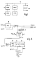
- Figure 1 is an overall block diagram of the multi-processor system, including a plurality of cache store units.
- Figure 2 shows one cache store unit in more detail.
- Figure 3 shows a physical address tag unit forming part of the cache store unit.
- Referring to Figure 1, the multi-processor system comprises a plurality of
processing units 10, and a sharedmain memory 11. Eachprocessing unit 10 has itsown cache unit 12. Thecache units 12 are all connected to themain memory 11 by way of a high speedprivate memory bus 13. - In operation, when a
processing unit 10 requires to read or write a data item, it sends the virtual address VA of that item to itscache unit 12. If the required data item is present in the cache, it can be accessed immediately by the processing unit, for reading or writing. Whenever one of theprocessors 10 updates a data item in itscache unit 12, the cache generates an update message over the bus to themain memory 11. This ensures that the main memory is kept consistent with the cache. - Each cache unit continuously monitors the
bus 13 for any update messages from the the other cache units. Whenever a cache detects such a message, it checks whether the updated data item is present in the cache and, if so, invalidates it. This ensures cache coherency. The way in which this is done will be described below. - Referring now to Figure 2, this shows one of the
cache units 12 in detail. - The cache comprises a data random-access memory (RAM) 20, holding 128K bytes. The RAM is organised as 4K individually addressable lines, each line holding 32 bytes. The data RAM is addressed by bits VA 5-16 of a 32-bit virtual address VA 0-31, so as to access one line of data for reading or writing. Bits VA 0-4 specify one byte within the address line, but are not used within the cache.
- The cache also includes a
VA tag RAM 21, which holds 4K tags, one for each line of data in the data RAM. Each tag represents bits VA 17-31 of the virtual address of the data held in this line. The VA tag RAM is addressed by bits VA 5-16. - The cache further includes a
status tag RAM 22, which holds 4K status tags, one for each line of the data RAM. Each of these tags includes a validity bit indicating whether or not the corresponding line of data is valid. The status tag RAM is also addressed by bits VA 5-16. - Whenever the
processing unit 10 requires to access a data item, it sends the virtual address VA 5-31 to the cache. Bits VA 5-16 access one line of the cache, and its corresponding VA tag and status tag. The VA tag from theRAM 21 is then compared with bits VA 17-31 of the virtual address from the processor, by means of acomparator 23. The result is then combined in anAND gate 24 with the validity bit for theRAM 22, so as to produce a HIT signal. - Thus, HIT is true only if the VA tag of the addressed line of data matches the corresponding bits of the virtual address, and that line is valid. The HIT signal therefore indicates to the processing unit that the required data is present in the cache, and can be read or updated as required.
- The cache unit also includes a memory management unit (MMU) 25, which translates the virtual address bits VA 5-31 into a physical address PA 5-31. The address space is divided into pages of 8K bytes. Bits VA 13-31 constitute a virtual page address, and are translated by the MMU into a corresponding physical page address PA 13-31. Bits VA 5-12 specify a line of 32 bytes within the page, and are used directly as the corresponding bits PA 5-12 of the physical address, without any translation.
- Whenever the processor updates a line of data in the cache, the cache sends an update message over the
bus 13 to the main memory. This update message includes the physical address bits PA 5-31, and also the updated value of the data line. - The cache unit continuously monitors the
bus 13 for update messages from other cache units. Whenever it detects such a message, it captures the physical address bits PA 5-31 of the message in aregister 26. - The PA from the
register 26 is applied to aPAtag logic circuit 27. As will be described in detail below, the PA tag logic holds as tags the physical addresses of all the lines of data currently in the cache. The PA tag logic effectively performs a parallel search on all the PA tags held in it, and this determines whether or not the corresponding line of data is held in the cache. If a match is detected, the PA tag logic outputs the virtual address bits VA 5-12, indicating the position of the data line in thedata RAM 20. These VA bits are then used to address thestatus tag RAM 22, and the validity bit of the addressed status tag is cleared. This invalidates the corresponding data line and hence ensures cache coherency. - It can be seen that the
PA tag logic 27 must effectively perform a comparison between the PA from the bus and the PA tags of all 4K lines in the cache. At first sight, this requires a large associative memory, capable of performing 4K comparisons in parallel. However, as will be shown, the present embodiment avoids the need for such a large number of simultaneous comparisons. - Referring now to Figure 3 this shows the PA tag logic in detail.
- This logic comprises sixteen PA tag RAMs 30, each of which holds 256 tags. There are thus 256 x 16 = 4K tags altogether, one for each of the data lines in the data RAM.
- All the
RAMs 30 are addressed in parallel by the outputs of amultiplexer 31, which selects either bits PA 5-12 from the bus (by way of register 26), or bits VA 5-12 from the processing unit. - Any one of the
RAMs 30 can be selected by meansof bits VA 13-16 from the processing unit. These bits are decoded by adecoder 32 to produce a write enable signal for the selected one of the RAMs. - All the tag RAMs 30 receive a common input signal from a
multiplexer 33, which selects either bits pA 13-31 from theMMU 25, or bits PA 13-31 from the bus. - Whenever a new line of data is loaded into the cache, the PA tag RAMs are addressed by VA 5-12 and VA 13-16, so as to select one tag in one of the RAMs. The physical address bits PA 13-31 from the MMU are then written into the selected tag, as a PA tag for the new line of data. In this way, the PA tag logic keeps tags indicating the physical addresses of all the data lines in the cache.
- Whenever an update message is detected in the bus, the tag RAMs 30 are all addressed by PA 5-12 from the bus. The bits PA 13-31 from the bus are then compared, in parallel, with the addressed tag in each of the tag RAMs, i.e. sixteen comparisons are performed in parallel, one by each of the tag RAMs. Each of the tag RAMs has a HIT output line, which indicates a match between the input PA 13-31 and the stored tag.
- For reasons to be explained below, only one (or none) of the HIT outputs will be true at any given time. The HIT outputs are applied to a 16:4
encoder 34, which encodes the position of the true HIT signal. The output of theencoder 34 thus reconstructs bits VA 13-16 of the virtual address of the data line with physical address equal to bits PA 5-21 from the bus. The reconstructed VA 13-16 from the encoder are combined with bits PA 5-12 from the bus, to provide the required virtual address VA 5-16 for invalidating the status tag RAM, as described above. - If, on the other hand, none of the HIT signals from the tag RAMS 30 are true, then the
encoder 34 produces a MISS signal, indicating that the data line in question is not present in the cache. - Thus, it can be seen that the PA tag logic shown in Figure 3 can check whether a data line with a particular PA tag is present in the cache, by performing only sixteen comparisons in parallel, rather than having to perform 4K comparisons. This is achieved by making use of the fact that, of the bits VA 5-16 which are used to address the cache RAMs, bits VA 5-12 are identical with bits PA 5-12 of the physical address; only bits VA 13-16 are different from the physical address. Hence, when a physical address is received from the bus, there are only 16 possible lines in the cache which might hold data with this PA.
- The PA tag RAMs 30 may be implemented, for example, by meas of four Fujitsu MB 81 C50 CMOS TAG Random Access Memories. Each of these devices provides a four-way tag RAM, including comparators for performing the tag comparisons, and can therefore be used to implement a group of four of the tags RAMs 30.
- In a virtual address memory system, several different virtual addresses may map on to the same physical address, these being referred to as synonyms. In general, this means that there may be more than one line in the cache corresponding to a particular physical address. In the present system, this is avoided by a software restriction, which requires that synonyms must be aligned on some multiple of 128K byte boundaries (i.e the size of the cache). This means that synonyms will all map on to he same line of the cache, and hence, at any given time, only one of them can be present in the cache. This is the reason why only one of the tag RAMs 30 can produce a HIT at any given time.
- In the above description, it was assumed that a "write through" strategy is adopted for updates, i.e. that the main store is updated whenever the cache is updated. However, it will be appreciated that the invention is equally applicable to storage systems using a "copy back" strategy, i.e. in which data is updated in the main store only when it is about to be overwritten in the cache and has been modified since it was loaded into the cache.
- Also in the above description, when a hit is detected by the PA tag logic, the corresponding data item is invalidated in the cache. Alternatively, the data item may be updated with the new value from the bus, which will also ensure cache coherency.
- It should be noted that the virtual address VA 0-31 may be extended in known manner by a context number to create a full virtual address.
Claims (6)
Applications Claiming Priority (2)
| Application Number | Priority Date | Filing Date | Title |
|---|---|---|---|
| GB8728494 | 1987-12-05 | ||
| GB878728494A GB8728494D0 (en) | 1987-12-05 | 1987-12-05 | Multi-cache data storage system |
Publications (3)
| Publication Number | Publication Date |
|---|---|
| EP0320099A2 true EP0320099A2 (en) | 1989-06-14 |
| EP0320099A3 EP0320099A3 (en) | 1990-08-22 |
| EP0320099B1 EP0320099B1 (en) | 1993-12-08 |
Family
ID=10628059
Family Applications (1)
| Application Number | Title | Priority Date | Filing Date |
|---|---|---|---|
| EP88309704A Expired - Lifetime EP0320099B1 (en) | 1987-12-05 | 1988-10-17 | Multi-cache data storage system |
Country Status (6)
| Country | Link |
|---|---|
| US (1) | US5008813A (en) |
| EP (1) | EP0320099B1 (en) |
| AU (1) | AU609228B2 (en) |
| DE (1) | DE3886182T2 (en) |
| GB (1) | GB8728494D0 (en) |
| ZA (1) | ZA888032B (en) |
Cited By (2)
| Publication number | Priority date | Publication date | Assignee | Title |
|---|---|---|---|---|
| EP0407219A2 (en) * | 1989-07-07 | 1991-01-09 | Fujitsu Limited | Data processing device |
| US5627992A (en) * | 1988-01-20 | 1997-05-06 | Advanced Micro Devices | Organization of an integrated cache unit for flexible usage in supporting microprocessor operations |
Families Citing this family (35)
| Publication number | Priority date | Publication date | Assignee | Title |
|---|---|---|---|---|
| GB8823077D0 (en) * | 1988-09-30 | 1988-11-09 | Int Computers Ltd | Data processing apparatus |
| US5535359A (en) * | 1988-12-02 | 1996-07-09 | Mitsubishi Denki Kabushiki Kaisha | Computer system with cache memory having address mask register |
| JPH0680499B2 (en) * | 1989-01-13 | 1994-10-12 | インターナショナル・ビジネス・マシーンズ・コーポレーション | Cache control system and method for multiprocessor system |
| US5214777A (en) * | 1989-03-27 | 1993-05-25 | Ncr Corporation | High speed read/modify/write memory system and method |
| US5072369A (en) * | 1989-04-07 | 1991-12-10 | Tektronix, Inc. | Interface between buses attached with cached modules providing address space mapped cache coherent memory access with SNOOP hit memory updates |
| FR2645986B1 (en) * | 1989-04-13 | 1994-06-17 | Bull Sa | METHOD FOR ACCELERATING MEMORY ACCESS OF A COMPUTER SYSTEM AND SYSTEM FOR IMPLEMENTING THE METHOD |
| FR2645987B1 (en) * | 1989-04-13 | 1991-06-07 | Bull Sa | MEMORY ACCESS ACCELERATION DEVICE IN A COMPUTER SYSTEM |
| US5197146A (en) * | 1989-06-21 | 1993-03-23 | Hewlett-Packard Company | Method for maintaining cache coherence in a multiprocessor computer system |
| US5155828A (en) * | 1989-07-05 | 1992-10-13 | Hewlett-Packard Company | Computing system with a cache memory and an additional look-aside cache memory |
| JPH0340046A (en) * | 1989-07-06 | 1991-02-20 | Hitachi Ltd | Cache memory control system and information processor |
| JPH0348951A (en) * | 1989-07-18 | 1991-03-01 | Fujitsu Ltd | Address monitor device |
| JPH0697449B2 (en) * | 1989-09-20 | 1994-11-30 | 株式会社日立製作所 | Multiplexed shared memory control method, multiplexed shared memory system and shared memory expansion method |
| JP2833062B2 (en) * | 1989-10-30 | 1998-12-09 | 株式会社日立製作所 | Cache memory control method, processor and information processing apparatus using the cache memory control method |
| US5297270A (en) * | 1989-11-13 | 1994-03-22 | Zenith Data Systems Corporation | Programmable cache memory which associates each section of main memory to be cached with a status bit which enables/disables the caching accessibility of the particular section, and with the capability of functioning with memory areas of varying size |
| JPH061463B2 (en) * | 1990-01-16 | 1994-01-05 | インターナショナル・ビジネス・マシーンズ・コーポレーション | Multiprocessor system and its private cache control method |
| US5263142A (en) * | 1990-04-12 | 1993-11-16 | Sun Microsystems, Inc. | Input/output cache with mapped pages allocated for caching direct (virtual) memory access input/output data based on type of I/O devices |
| US5249284A (en) * | 1990-06-04 | 1993-09-28 | Ncr Corporation | Method and system for maintaining data coherency between main and cache memories |
| US5276852A (en) * | 1990-10-01 | 1994-01-04 | Digital Equipment Corporation | Method and apparatus for controlling a processor bus used by multiple processor components during writeback cache transactions |
| US5301340A (en) * | 1990-10-31 | 1994-04-05 | International Business Machines Corporation | IC chips including ALUs and identical register files whereby a number of ALUs directly and concurrently write results to every register file per cycle |
| US5249283A (en) * | 1990-12-24 | 1993-09-28 | Ncr Corporation | Cache coherency method and apparatus for a multiple path interconnection network |
| GB2260429B (en) * | 1991-10-11 | 1995-05-24 | Intel Corp | Versatile cache memory |
| US5414827A (en) * | 1991-12-19 | 1995-05-09 | Opti, Inc. | Automatic cache flush |
| US5469555A (en) * | 1991-12-19 | 1995-11-21 | Opti, Inc. | Adaptive write-back method and apparatus wherein the cache system operates in a combination of write-back and write-through modes for a cache-based microprocessor system |
| US5555382A (en) * | 1992-04-24 | 1996-09-10 | Digital Equipment Corporation | Intelligent snoopy bus arbiter |
| US5778424A (en) * | 1993-04-30 | 1998-07-07 | Avsys Corporation | Distributed placement, variable-size cache architecture |
| US5671391A (en) * | 1994-01-10 | 1997-09-23 | Ncr Corporation | Coherent copyback protocol for multi-level cache memory systems |
| US6928521B1 (en) | 2000-08-01 | 2005-08-09 | International Business Machines Corporation | Method, system, and data structures for using metadata in updating data in a storage device |
| US7681141B2 (en) * | 2004-05-11 | 2010-03-16 | Sony Computer Entertainment America Inc. | Fast scrolling in a graphical user interface |
| JP4189402B2 (en) * | 2005-02-21 | 2008-12-03 | パナソニック株式会社 | Cache circuit |
| US7409524B2 (en) * | 2005-08-17 | 2008-08-05 | Hewlett-Packard Development Company, L.P. | System and method for responding to TLB misses |
| US8806101B2 (en) * | 2008-12-30 | 2014-08-12 | Intel Corporation | Metaphysical address space for holding lossy metadata in hardware |
| US8627017B2 (en) * | 2008-12-30 | 2014-01-07 | Intel Corporation | Read and write monitoring attributes in transactional memory (TM) systems |
| US8627014B2 (en) * | 2008-12-30 | 2014-01-07 | Intel Corporation | Memory model for hardware attributes within a transactional memory system |
| US9785462B2 (en) | 2008-12-30 | 2017-10-10 | Intel Corporation | Registering a user-handler in hardware for transactional memory event handling |
| US10592424B2 (en) * | 2017-07-14 | 2020-03-17 | Arm Limited | Range-based memory system |
Citations (1)
| Publication number | Priority date | Publication date | Assignee | Title |
|---|---|---|---|---|
| EP0232526A2 (en) * | 1985-12-19 | 1987-08-19 | Bull HN Information Systems Inc. | Paged virtual cache system |
Family Cites Families (14)
| Publication number | Priority date | Publication date | Assignee | Title |
|---|---|---|---|---|
| US3699533A (en) * | 1970-10-29 | 1972-10-17 | Rca Corp | Memory system including buffer memories |
| US3693165A (en) * | 1971-06-29 | 1972-09-19 | Ibm | Parallel addressing of a storage hierarchy in a data processing system using virtual addressing |
| US3848234A (en) * | 1973-04-04 | 1974-11-12 | Sperry Rand Corp | Multi-processor system with multiple cache memories |
| US4453230A (en) * | 1977-12-29 | 1984-06-05 | Tokyo Shibaura Electric Co., Ltd. | Address conversion system |
| US4445191A (en) * | 1979-08-13 | 1984-04-24 | Burroughs Corporation | Data word handling enhancement in a page oriented named-data hierarchical memory system |
| FR2474201B1 (en) * | 1980-01-22 | 1986-05-16 | Bull Sa | METHOD AND DEVICE FOR MANAGING CONFLICTS CAUSED BY MULTIPLE ACCESSES TO THE SAME CACH OF A DIGITAL INFORMATION PROCESSING SYSTEM COMPRISING AT LEAST TWO PROCESSES EACH HAVING A CACHE |
| US4481573A (en) * | 1980-11-17 | 1984-11-06 | Hitachi, Ltd. | Shared virtual address translation unit for a multiprocessor system |
| US4602368A (en) * | 1983-04-15 | 1986-07-22 | Honeywell Information Systems Inc. | Dual validity bit arrays |
| US4858111A (en) * | 1983-07-29 | 1989-08-15 | Hewlett-Packard Company | Write-back cache system using concurrent address transfers to setup requested address in main memory before dirty miss signal from cache |
| US4785395A (en) * | 1986-06-27 | 1988-11-15 | Honeywell Bull Inc. | Multiprocessor coherent cache system including two level shared cache with separately allocated processor storage locations and inter-level duplicate entry replacement |
| US4843542A (en) * | 1986-11-12 | 1989-06-27 | Xerox Corporation | Virtual memory cache for use in multi-processing systems |
| US4977498A (en) * | 1988-04-01 | 1990-12-11 | Digital Equipment Corporation | Data processing system having a data memory interlock coherency scheme |
| JPH03505793A (en) * | 1988-07-04 | 1991-12-12 | スウェーディッシュ インスティテュート オブ コンピューター サイエンス | Multiprocessor system including cache memory system with hierarchical structure |
| GB8823077D0 (en) * | 1988-09-30 | 1988-11-09 | Int Computers Ltd | Data processing apparatus |
-
1987
- 1987-12-05 GB GB878728494A patent/GB8728494D0/en active Pending
-
1988
- 1988-10-17 DE DE88309704T patent/DE3886182T2/en not_active Expired - Fee Related
- 1988-10-17 EP EP88309704A patent/EP0320099B1/en not_active Expired - Lifetime
- 1988-10-21 US US07/261,033 patent/US5008813A/en not_active Expired - Fee Related
- 1988-10-26 ZA ZA888032A patent/ZA888032B/en unknown
- 1988-12-02 AU AU26541/88A patent/AU609228B2/en not_active Ceased
Patent Citations (1)
| Publication number | Priority date | Publication date | Assignee | Title |
|---|---|---|---|---|
| EP0232526A2 (en) * | 1985-12-19 | 1987-08-19 | Bull HN Information Systems Inc. | Paged virtual cache system |
Non-Patent Citations (1)
| Title |
|---|
| COMPUTING SURVEYS, vol. 14, no. 3, September 1982, pages 473-530, New York, US; A.J. SMITH: ""Cache memories" * |
Cited By (4)
| Publication number | Priority date | Publication date | Assignee | Title |
|---|---|---|---|---|
| US5627992A (en) * | 1988-01-20 | 1997-05-06 | Advanced Micro Devices | Organization of an integrated cache unit for flexible usage in supporting microprocessor operations |
| EP0407219A2 (en) * | 1989-07-07 | 1991-01-09 | Fujitsu Limited | Data processing device |
| EP0407219A3 (en) * | 1989-07-07 | 1992-09-02 | Fujitsu Limited | Data processing device |
| US5440696A (en) * | 1989-07-07 | 1995-08-08 | Fujitsu Limited | Data processing device for reducing the number of internal bus lines |
Also Published As
| Publication number | Publication date |
|---|---|
| GB8728494D0 (en) | 1988-01-13 |
| ZA888032B (en) | 1989-06-28 |
| DE3886182D1 (en) | 1994-01-20 |
| AU2654188A (en) | 1989-06-08 |
| EP0320099B1 (en) | 1993-12-08 |
| DE3886182T2 (en) | 1994-05-05 |
| US5008813A (en) | 1991-04-16 |
| AU609228B2 (en) | 1991-04-26 |
| EP0320099A3 (en) | 1990-08-22 |
Similar Documents
| Publication | Publication Date | Title |
|---|---|---|
| EP0320099B1 (en) | Multi-cache data storage system | |
| US4785398A (en) | Virtual cache system using page level number generating CAM to access other memories for processing requests relating to a page | |
| US5361340A (en) | Apparatus for maintaining consistency in a multiprocessor computer system using virtual caching | |
| US5133058A (en) | Page-tagging translation look-aside buffer for a computer memory system | |
| US3761881A (en) | Translation storage scheme for virtual memory system | |
| US3723976A (en) | Memory system with logical and real addressing | |
| AU608447B2 (en) | Data memory system | |
| EP0596636B1 (en) | Cache tag memory | |
| US6804741B2 (en) | Coherent memory mapping tables for host I/O bridge | |
| US4654790A (en) | Translation of virtual and real addresses to system addresses | |
| US5140681A (en) | Multi-processing system and cache apparatus for use in the same | |
| US5479630A (en) | Hybrid cache having physical-cache and virtual-cache characteristics and method for accessing same | |
| KR100285533B1 (en) | Write-Through Virtual Cache Memory, Alias Addressing, and Cache Flush | |
| US5179675A (en) | Data processing system with cache memory addressable by virtual and physical address | |
| US5530823A (en) | Hit enhancement circuit for page-table-look-aside-buffer | |
| US4736287A (en) | Set association memory system | |
| US5463750A (en) | Method and apparatus for translating virtual addresses in a data processing system having multiple instruction pipelines and separate TLB's | |
| EP0439952A2 (en) | Dual-port cache tag memory | |
| US6021481A (en) | Effective-to-real address cache managing apparatus and method | |
| US5386530A (en) | Address translation device capable of obtaining a real address from a virtual address in a shorter time | |
| EP0474356A1 (en) | Cache memory and operating method | |
| US6931510B1 (en) | Method and system for translation lookaside buffer coherence in multiprocessor systems | |
| JPH0383150A (en) | Control system for cache device with address converting mechanism | |
| JPH05216767A (en) | Entry replacement control system | |
| JPS63259748A (en) | Hierarchical storage control system |
Legal Events
| Date | Code | Title | Description |
|---|---|---|---|
| PUAI | Public reference made under article 153(3) epc to a published international application that has entered the european phase |
Free format text: ORIGINAL CODE: 0009012 |
|
| AK | Designated contracting states |
Kind code of ref document: A2 Designated state(s): DE FR GB IT NL |
|
| PUAL | Search report despatched |
Free format text: ORIGINAL CODE: 0009013 |
|
| AK | Designated contracting states |
Kind code of ref document: A3 Designated state(s): DE FR GB IT NL |
|
| 17P | Request for examination filed |
Effective date: 19900809 |
|
| 17Q | First examination report despatched |
Effective date: 19921106 |
|
| ITF | It: translation for a ep patent filed |
Owner name: BARZANO' E ZANARDO ROMA S.P.A. |
|
| GRAA | (expected) grant |
Free format text: ORIGINAL CODE: 0009210 |
|
| AK | Designated contracting states |
Kind code of ref document: B1 Designated state(s): DE FR GB IT NL |
|
| REF | Corresponds to: |
Ref document number: 3886182 Country of ref document: DE Date of ref document: 19940120 |
|
| ET | Fr: translation filed | ||
| PLBE | No opposition filed within time limit |
Free format text: ORIGINAL CODE: 0009261 |
|
| STAA | Information on the status of an ep patent application or granted ep patent |
Free format text: STATUS: NO OPPOSITION FILED WITHIN TIME LIMIT |
|
| 26N | No opposition filed | ||
| PGFP | Annual fee paid to national office [announced via postgrant information from national office to epo] |
Ref country code: NL Payment date: 19980923 Year of fee payment: 11 |
|
| PGFP | Annual fee paid to national office [announced via postgrant information from national office to epo] |
Ref country code: FR Payment date: 19990914 Year of fee payment: 12 |
|
| PGFP | Annual fee paid to national office [announced via postgrant information from national office to epo] |
Ref country code: DE Payment date: 19990930 Year of fee payment: 12 |
|
| PG25 | Lapsed in a contracting state [announced via postgrant information from national office to epo] |
Ref country code: NL Free format text: LAPSE BECAUSE OF NON-PAYMENT OF DUE FEES Effective date: 20000501 |
|
| NLV4 | Nl: lapsed or anulled due to non-payment of the annual fee |
Effective date: 20000501 |
|
| PG25 | Lapsed in a contracting state [announced via postgrant information from national office to epo] |
Ref country code: FR Free format text: LAPSE BECAUSE OF NON-PAYMENT OF DUE FEES Effective date: 20010629 |
|
| PG25 | Lapsed in a contracting state [announced via postgrant information from national office to epo] |
Ref country code: DE Free format text: LAPSE BECAUSE OF NON-PAYMENT OF DUE FEES Effective date: 20010703 |
|
| REG | Reference to a national code |
Ref country code: FR Ref legal event code: ST |
|
| REG | Reference to a national code |
Ref country code: GB Ref legal event code: IF02 |
|
| PGFP | Annual fee paid to national office [announced via postgrant information from national office to epo] |
Ref country code: GB Payment date: 20030901 Year of fee payment: 16 |
|
| PG25 | Lapsed in a contracting state [announced via postgrant information from national office to epo] |
Ref country code: GB Free format text: LAPSE BECAUSE OF NON-PAYMENT OF DUE FEES Effective date: 20041017 |
|
| GBPC | Gb: european patent ceased through non-payment of renewal fee |
Effective date: 20041017 |
|
| PG25 | Lapsed in a contracting state [announced via postgrant information from national office to epo] |
Ref country code: IT Free format text: LAPSE BECAUSE OF NON-PAYMENT OF DUE FEES;WARNING: LAPSES OF ITALIAN PATENTS WITH EFFECTIVE DATE BEFORE 2007 MAY HAVE OCCURRED AT ANY TIME BEFORE 2007. THE CORRECT EFFECTIVE DATE MAY BE DIFFERENT FROM THE ONE RECORDED. Effective date: 20051017 |