EP0320970A2 - Vapour-phase epitaxial growth process - Google Patents
Vapour-phase epitaxial growth process Download PDFInfo
- Publication number
- EP0320970A2 EP0320970A2 EP88121113A EP88121113A EP0320970A2 EP 0320970 A2 EP0320970 A2 EP 0320970A2 EP 88121113 A EP88121113 A EP 88121113A EP 88121113 A EP88121113 A EP 88121113A EP 0320970 A2 EP0320970 A2 EP 0320970A2
- Authority
- EP
- European Patent Office
- Prior art keywords
- epitaxial growth
- vapor
- phase epitaxial
- growth process
- ing
- Prior art date
- Legal status (The legal status is an assumption and is not a legal conclusion. Google has not performed a legal analysis and makes no representation as to the accuracy of the status listed.)
- Granted
Links
Images


Classifications
-
- H—ELECTRICITY
- H01—ELECTRIC ELEMENTS
- H01L—SEMICONDUCTOR DEVICES NOT COVERED BY CLASS H10
- H01L21/00—Processes or apparatus adapted for the manufacture or treatment of semiconductor or solid state devices or of parts thereof
- H01L21/02—Manufacture or treatment of semiconductor devices or of parts thereof
- H01L21/04—Manufacture or treatment of semiconductor devices or of parts thereof the devices having at least one potential-jump barrier or surface barrier, e.g. PN junction, depletion layer or carrier concentration layer
- H01L21/18—Manufacture or treatment of semiconductor devices or of parts thereof the devices having at least one potential-jump barrier or surface barrier, e.g. PN junction, depletion layer or carrier concentration layer the devices having semiconductor bodies comprising elements of Group IV of the Periodic System or AIIIBV compounds with or without impurities, e.g. doping materials
- H01L21/20—Deposition of semiconductor materials on a substrate, e.g. epitaxial growth solid phase epitaxy
-
- H—ELECTRICITY
- H01—ELECTRIC ELEMENTS
- H01L—SEMICONDUCTOR DEVICES NOT COVERED BY CLASS H10
- H01L21/00—Processes or apparatus adapted for the manufacture or treatment of semiconductor or solid state devices or of parts thereof
- H01L21/70—Manufacture or treatment of devices consisting of a plurality of solid state components formed in or on a common substrate or of parts thereof; Manufacture of integrated circuit devices or of parts thereof
- H01L21/71—Manufacture of specific parts of devices defined in group H01L21/70
- H01L21/74—Making of localized buried regions, e.g. buried collector layers, internal connections substrate contacts
-
- H—ELECTRICITY
- H01—ELECTRIC ELEMENTS
- H01L—SEMICONDUCTOR DEVICES NOT COVERED BY CLASS H10
- H01L21/00—Processes or apparatus adapted for the manufacture or treatment of semiconductor or solid state devices or of parts thereof
- H01L21/02—Manufacture or treatment of semiconductor devices or of parts thereof
- H01L21/02104—Forming layers
- H01L21/02365—Forming inorganic semiconducting materials on a substrate
- H01L21/02367—Substrates
- H01L21/0237—Materials
- H01L21/02373—Group 14 semiconducting materials
- H01L21/02381—Silicon, silicon germanium, germanium
-
- H—ELECTRICITY
- H01—ELECTRIC ELEMENTS
- H01L—SEMICONDUCTOR DEVICES NOT COVERED BY CLASS H10
- H01L21/00—Processes or apparatus adapted for the manufacture or treatment of semiconductor or solid state devices or of parts thereof
- H01L21/02—Manufacture or treatment of semiconductor devices or of parts thereof
- H01L21/02104—Forming layers
- H01L21/02365—Forming inorganic semiconducting materials on a substrate
- H01L21/02367—Substrates
- H01L21/0237—Materials
- H01L21/0242—Crystalline insulating materials
-
- H—ELECTRICITY
- H01—ELECTRIC ELEMENTS
- H01L—SEMICONDUCTOR DEVICES NOT COVERED BY CLASS H10
- H01L21/00—Processes or apparatus adapted for the manufacture or treatment of semiconductor or solid state devices or of parts thereof
- H01L21/02—Manufacture or treatment of semiconductor devices or of parts thereof
- H01L21/02104—Forming layers
- H01L21/02365—Forming inorganic semiconducting materials on a substrate
- H01L21/02518—Deposited layers
- H01L21/02521—Materials
- H01L21/02524—Group 14 semiconducting materials
- H01L21/02532—Silicon, silicon germanium, germanium
-
- H—ELECTRICITY
- H01—ELECTRIC ELEMENTS
- H01L—SEMICONDUCTOR DEVICES NOT COVERED BY CLASS H10
- H01L21/00—Processes or apparatus adapted for the manufacture or treatment of semiconductor or solid state devices or of parts thereof
- H01L21/02—Manufacture or treatment of semiconductor devices or of parts thereof
- H01L21/02104—Forming layers
- H01L21/02365—Forming inorganic semiconducting materials on a substrate
- H01L21/02518—Deposited layers
- H01L21/0257—Doping during depositing
- H01L21/02573—Conductivity type
- H01L21/02576—N-type
-
- H—ELECTRICITY
- H01—ELECTRIC ELEMENTS
- H01L—SEMICONDUCTOR DEVICES NOT COVERED BY CLASS H10
- H01L21/00—Processes or apparatus adapted for the manufacture or treatment of semiconductor or solid state devices or of parts thereof
- H01L21/02—Manufacture or treatment of semiconductor devices or of parts thereof
- H01L21/02104—Forming layers
- H01L21/02365—Forming inorganic semiconducting materials on a substrate
- H01L21/02518—Deposited layers
- H01L21/0257—Doping during depositing
- H01L21/02573—Conductivity type
- H01L21/02579—P-type
-
- H—ELECTRICITY
- H01—ELECTRIC ELEMENTS
- H01L—SEMICONDUCTOR DEVICES NOT COVERED BY CLASS H10
- H01L21/00—Processes or apparatus adapted for the manufacture or treatment of semiconductor or solid state devices or of parts thereof
- H01L21/02—Manufacture or treatment of semiconductor devices or of parts thereof
- H01L21/02104—Forming layers
- H01L21/02365—Forming inorganic semiconducting materials on a substrate
- H01L21/02612—Formation types
- H01L21/02617—Deposition types
- H01L21/0262—Reduction or decomposition of gaseous compounds, e.g. CVD
-
- H—ELECTRICITY
- H01—ELECTRIC ELEMENTS
- H01L—SEMICONDUCTOR DEVICES NOT COVERED BY CLASS H10
- H01L21/00—Processes or apparatus adapted for the manufacture or treatment of semiconductor or solid state devices or of parts thereof
- H01L21/02—Manufacture or treatment of semiconductor devices or of parts thereof
- H01L21/04—Manufacture or treatment of semiconductor devices or of parts thereof the devices having at least one potential-jump barrier or surface barrier, e.g. PN junction, depletion layer or carrier concentration layer
- H01L21/18—Manufacture or treatment of semiconductor devices or of parts thereof the devices having at least one potential-jump barrier or surface barrier, e.g. PN junction, depletion layer or carrier concentration layer the devices having semiconductor bodies comprising elements of Group IV of the Periodic System or AIIIBV compounds with or without impurities, e.g. doping materials
- H01L21/22—Diffusion of impurity materials, e.g. doping materials, electrode materials, into or out of a semiconductor body, or between semiconductor regions; Interactions between two or more impurities; Redistribution of impurities
- H01L21/2205—Diffusion of impurity materials, e.g. doping materials, electrode materials, into or out of a semiconductor body, or between semiconductor regions; Interactions between two or more impurities; Redistribution of impurities from the substrate during epitaxy, e.g. autodoping; Preventing or using autodoping
-
- Y—GENERAL TAGGING OF NEW TECHNOLOGICAL DEVELOPMENTS; GENERAL TAGGING OF CROSS-SECTIONAL TECHNOLOGIES SPANNING OVER SEVERAL SECTIONS OF THE IPC; TECHNICAL SUBJECTS COVERED BY FORMER USPC CROSS-REFERENCE ART COLLECTIONS [XRACs] AND DIGESTS
- Y10—TECHNICAL SUBJECTS COVERED BY FORMER USPC
- Y10S—TECHNICAL SUBJECTS COVERED BY FORMER USPC CROSS-REFERENCE ART COLLECTIONS [XRACs] AND DIGESTS
- Y10S148/00—Metal treatment
- Y10S148/007—Autodoping
-
- Y—GENERAL TAGGING OF NEW TECHNOLOGICAL DEVELOPMENTS; GENERAL TAGGING OF CROSS-SECTIONAL TECHNOLOGIES SPANNING OVER SEVERAL SECTIONS OF THE IPC; TECHNICAL SUBJECTS COVERED BY FORMER USPC CROSS-REFERENCE ART COLLECTIONS [XRACs] AND DIGESTS
- Y10—TECHNICAL SUBJECTS COVERED BY FORMER USPC
- Y10S—TECHNICAL SUBJECTS COVERED BY FORMER USPC CROSS-REFERENCE ART COLLECTIONS [XRACs] AND DIGESTS
- Y10S148/00—Metal treatment
- Y10S148/025—Deposition multi-step
-
- Y—GENERAL TAGGING OF NEW TECHNOLOGICAL DEVELOPMENTS; GENERAL TAGGING OF CROSS-SECTIONAL TECHNOLOGIES SPANNING OVER SEVERAL SECTIONS OF THE IPC; TECHNICAL SUBJECTS COVERED BY FORMER USPC CROSS-REFERENCE ART COLLECTIONS [XRACs] AND DIGESTS
- Y10—TECHNICAL SUBJECTS COVERED BY FORMER USPC
- Y10S—TECHNICAL SUBJECTS COVERED BY FORMER USPC CROSS-REFERENCE ART COLLECTIONS [XRACs] AND DIGESTS
- Y10S148/00—Metal treatment
- Y10S148/169—Vacuum deposition, e.g. including molecular beam epitaxy
Definitions
- the present invention relates to a vapor-phase epitaxial growth process performed on a silicon wafer having a buried layer of a high impurity concentration.
- Precise control of an impurity dopant in a semi-conductor substrate and a high concentration of the impurity dopant are essential for obtaining high-performance, high-speed bipolar integrated circuits (ICs) and Bi-CMOS ICs. Also, for reducing parasitic capacity, reduction in size of elements, for example, by trench isolation, has been proposed.
- a silicon wafer for high-speed bipolar ICs or Bi-CMOS ICs includes a high concentration impurity buried layer.
- antimony (Sb) is conventionally used as a dopant for an N+ buried layer.
- an As or B ion-implanted substrate formed by implanting As ions or B ions in a buried layer which has an atomic radius matching with a silicon wafer so that the concentration of doping can be increased.
- an epitaxial growth is performed on the As or B ion-implanted substrate, a problem of auto-doping from the buried layer occurs.
- the following methods are available, though they have problems:
- the object of the present invention is to solve the above-mentioned problems in performing a vapor-phase epitaxial growth on a silicon wafer having a buried layer of a high As or B concentration, that if the auto-doping from the buried layer is to be suppressed, the depth xj of the buried layer is increased, and the dopant is evaporated to lower the concentration of the buried layer, resulting in a low productivity rate.
- the object of this invention is to provide a vapor-phase epitaxial growth process wherein the variations in depth xj of the high-concentration buried layer and in concentration of the dopant can be remarkably suppressed, and an epitaxial growth layer can be manufactured at high productivity rate with the auto-doping being suppressed.
- the present lnvention provides a vapor-phase epitaxial growth process comprising:
- step (i) is, preferivelyably, between 600°C to 800°C.
- Step (i) may be performed while the temperature of the silicon wafer is rising, or is kept constant. However, from the viewpoint of the productivity rate, it is desirable that step (i) be performed while the temperature of the silicon wafer is rising.
- the pressure employed in step (i) be, preferably, not higher than 100 torr. If step (i) is performed under pressure of 100 torr or below, the growth can easily be performed at low temperature. When an epitaxial growth is to be performed on a wafer of large-diameter, the low-temperature processing is advantageous to prevent the slip in crystal structure.
- the silicon wafer may be of a twin tub structure consisting of a high boron concentration buried layer and a high concentration arsenic concentration buried layer.
- the thickness of the first epitaxial layer may be 0.3 ⁇ m or less. From the viewpoint of productivity rate, the thickness of the first epitaxial layer should preferably be 0.05 ⁇ m or less.
- the mixing ratio of the silane fluoride to the silane of the reaction gas used in step (i) is optimally 5-30 : 1, in order to grow a high quality singlecrystal.
- the temperature should be kept, at a relatively high temperature for example, 850°C, so that the epitaxial growth proceeds at a growth rate of 0.05 ⁇ m/min or more, preferably, 0.1 ⁇ m/min or more.
- the reaction gas employed therein is highly effective in allowing the epitaxial layer to grow at a low temperature.
- the impurity concentration distribution in the depth direction, and the concentration of the dopant can be precisely controlled.
- the epitaxial layer can be formed at high productivity rate. Therefore, variations in depth xj of the high impurity concentration buried layer and in concentration of the dopant can be remarkably suppressed, and the epitaxial layer wherein auto-doping is prevented can be manufactured at high productivity rate.
- Fig. 1 schematically shows a vertical-type reaction apparatus as an example of a vapor-phase epitaxial growth apparatus used in a process of the present invention.
- Bell-jar 1 is made of quartz.
- Rotatable susceptor 2 is arranged within bell-jar 1.
- Silicon wafer 3 is placed on susceptor 2.
- Heating coil 4 heats wafer 3.
- a reaction gas is supplied from external gas control device 5 to gas pipe 6. The gas is discharged through a nozzle of gas pipe 6 to the upper inner region of bell-jar 1.
- Gas outlet 7 is provided at the bottom of bell-jar 1.
- Heating coil 4 heats wafer 3 by high-frequency heating method.
- wafer 3 can be heated by any other heating method, as long as the temperature of wafer 3 can be desirably controlled.
- the reaction apparatus is not limited to the above-mentioned vertical-type furnace.
- a raw feed gas containing a mixture of SiH2F2 (silane difluoride) gas and Si2H6 (disilane) gas, the ratio thereof being, e.g., 10 : 1, and a carrier gas (e.g., H2 gas) are supplied to bell-jar 1.
- the raw feed gas is heated at a temperature ranging 600°C to 900°C under a pressure of 100 torr or below, thus forming a first epitaxial layer having a thickness of up to 0.3 ⁇ m.
- Si2H6 is employed as a raw feed gas.
- the gas is heated to a fixed temperature of, e.g., 850°C and the epitaxial growth process is performed at a suitable growth rate (e.g., 0.1 ⁇ m/min or above). This growth rate may be suitably selected by taking into consideration a productivity rate.
- Doping can be performed in either of the first epitaxial growth step or the second epitaxial growth step.
- the process of the present invention can be used in the case where a slight amount of halogenated silane such as chloride coexists with silane fluoride.
- the first epitaxial step employs the specific reaction gas which allows the first epitaxial layer to grow at a relatively low temperature.
- the impurity concentration distribution in the depth direction of the buried layer can be precisely controlled, and the variations in depth xj of the buried layer and in As concentration can be suppressed.
- the second epitaxial growth step the growth of the second epitaxial layer is performed at a growth rate higher than that of the first epitaxial growth step.
- the productivity rate can be increased, and all steps of the process can be completed within an hour.
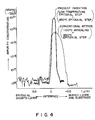
- Fig. 3 shows data indicating the relationship between the epitaxial growth temperature, on one hand, and the depth xj of the buried layer and the width of the transition region of the impurity concentration, on the other hand. It is understood that, when growth temperature T is low, the depth xj is small and the width of the transition region is also small.
- a thick line indicates the data of the impurity concentration distribution in the depth direction of the substrate formed of the silicon wafer according to the process of the present invention.
- a thin line indicates the data of an impurity concentration distribution in the case of a conventional process (in which a silicon wafer is subjected to an annealing step at 1100°C and, thereafter, an epitaxial growth is performed at 850°C). It is understood that, according to the example of the present invention, the depth xj of the high-concentration As-buried layer does not considerably increase, and the impurity concentration distribution in the depth direction is exactly controlled.
- a dose of As ions amounting to 5 x 1015cm ⁇ 2 is injected at an acceleration voltage of 50 keV, and an epitaxial process is performed without subjecting it to a drive-in process through annealing.
- a heating process is performed at a temperature of 900°C or below, as in the example of the present invention, the peak value of the As concentration is 1021/cm3.
- the heating step is performed at a temperature of 1100°C or above, as in the conventional method, the peak value of the As concentration is 6 ⁇ 1019cm3.
- the peak value of the As concentration in the example according to the present invention is higher than that in the conventional method. Consequently, according to the present invention, a drive-in step after ion implantation is not necessary.
- the reaction gas used in the first epitaxial growth step was the mixture gas containing silane difluoride and disilane.
- a mixture gas which is different from that of above example, i.e., a mixture of other silane fluoride and/or disilane fluoride with silane and/or disilane.
- disilane gas was used in the second epitaxial growth step.
- the same advantages as were obtained in the above example can be obtained with the use of monosilane or a mixture of monosilane and disilane, or a mixture gas of these silanes and at least one of compounds selected from silane fluoride and disilane fluoride.
Abstract
Description
- The present invention relates to a vapor-phase epitaxial growth process performed on a silicon wafer having a buried layer of a high impurity concentration.
- Precise control of an impurity dopant in a semi-conductor substrate and a high concentration of the impurity dopant are essential for obtaining high-performance, high-speed bipolar integrated circuits (ICs) and Bi-CMOS ICs. Also, for reducing parasitic capacity, reduction in size of elements, for example, by trench isolation, has been proposed.
- A silicon wafer for high-speed bipolar ICs or Bi-CMOS ICs includes a high concentration impurity buried layer. For example, antimony (Sb) is conventionally used as a dopant for an N⁺ buried layer.
- When Sb is used as a dopant, however, the following problems occur:
- a) The solid solubility of Sb in silicon is - 5 × 10¹⁹/cm³ at 1200°C, which is lower than 10²¹/cm³ of arsenic (As). Thus, the obtaining of a buried layer of high impurity concentration is restricted.
- b) The atomic radius of Si is 1.17 Å, that of Sb is 1.36 Å, and that of As is 1.17 Å. When Sb is doped in a silicon wafer at high concentration, mismatch of atomic radius occurs, resulting in distortion of an epitaxial growth film.
- Under the circumstance, it is proposed to use an As or B ion-implanted substrate formed by implanting As ions or B ions in a buried layer which has an atomic radius matching with a silicon wafer so that the concentration of doping can be increased. However, when an epitaxial growth is performed on the As or B ion-implanted substrate, a problem of auto-doping from the buried layer occurs. In order to suppress the auto-doping, the following methods are available, though they have problems:
- (a) Reduced pressure epitaxy growth method: An epitaxial growth is performed in reduced pressure at a temperature of 1050°C or above. Since a high-temperature step is performed, the depth xj of the embedded layer is undesirably increased, and the As dopant is evaporated and the concentration of impurity in the buried layer is lowered.
- (b) A photo-epitaxial growth method: With this method, all steps are performed at low temperature. This method is still in an experimental stage, and has not yet been put into practice. This method has a problem of productivity rate.
- (c) A two-stage epitaxial growth method. In a first epitaxial growth process, a non-doped epitaxial film is made to grow, and in a second epitaxial growth process, a doped epitaxial film of a desired impurity concentration is made to grow. However, due to a particular reaction gas to be used, a high-temperature process must be performed. Thus, the depth xj of the buried layer is increased, and the dopant (As) is evaporated, resulting in a decrease in concentration of the buried layer.
- The object of the present invention is to solve the above-mentioned problems in performing a vapor-phase epitaxial growth on a silicon wafer having a buried layer of a high As or B concentration, that if the auto-doping from the buried layer is to be suppressed, the depth xj of the buried layer is increased, and the dopant is evaporated to lower the concentration of the buried layer, resulting in a low productivity rate.
- Namely, the object of this invention is to provide a vapor-phase epitaxial growth process wherein the variations in depth xj of the high-concentration buried layer and in concentration of the dopant can be remarkably suppressed, and an epitaxial growth layer can be manufactured at high productivity rate with the auto-doping being suppressed.
- In order to achieve the object of the invention, the present lnvention provides a vapor-phase epitaxial growth process comprising:
- (i) a step of performing a gas-phase epitaxial growth at a temperature of 600°C to 900°C by using a reaction gas containing at least one kind selected from a group consisting of SiHxF4-x (x = 0 to 3) and Si₂HxF6-x (x = 0-5), and at least one kind selected from a group consisting of SiH₄ and Si₂H₆, thereby to form a first epitaxial layer on a silicon wafer having a high impurity concentration buried layer containing arsenic (As) or boron (B) as a dopant; and
- (ii) a step of performing a gas-phase epitaxial growth at a growth rate higher than that performed in step (i) by using a reaction gas containing at least one kine of silane selected from a group consisting of SiH₄ and Si₂H₆, or a reaction gas containing at least one kind of the silane and at least one kind of silane fluoride selected from a group consisting of SiHxF4-x (x = 0 to 3) and Si₂HxF6-x (x = 0-5), thereby forming a second epitaxlal layer on said first epitaxial layer.
- The temperature employed in step (i) is, preferably, between 600°C to 800°C. Step (i) may be performed while the temperature of the silicon wafer is rising, or is kept constant. However, from the viewpoint of the productivity rate, it is desirable that step (i) be performed while the temperature of the silicon wafer is rising. The pressure employed in step (i) be, preferably, not higher than 100 torr. If step (i) is performed under pressure of 100 torr or below, the growth can easily be performed at low temperature. When an epitaxial growth is to be performed on a wafer of large-diameter, the low-temperature processing is advantageous to prevent the slip in crystal structure. The silicon wafer may be of a twin tub structure consisting of a high boron concentration buried layer and a high concentration arsenic concentration buried layer. The thickness of the first epitaxial layer may be 0.3 µm or less. From the viewpoint of productivity rate, the thickness of the first epitaxial layer should preferably be 0.05 µm or less. The mixing ratio of the silane fluoride to the silane of the reaction gas used in step (i) is optimally 5-30 : 1, in order to grow a high quality singlecrystal. In step (ii) however, in view of productivity, the temperature should be kept, at a relatively high temperature for example, 850°C, so that the epitaxial growth proceeds at a growth rate of 0.05 µm/min or more, preferably, 0.1 µm/min or more.
- According to the present invention, as stated above, in the first epitaxial step, the reaction gas employed therein is highly effective in allowing the epitaxial layer to grow at a low temperature. Thus, the impurity concentration distribution in the depth direction, and the concentration of the dopant can be precisely controlled. In the second epitaxial growth process, the epitaxial layer can be formed at high productivity rate. Therefore, variations in depth xj of the high impurity concentration buried layer and in concentration of the dopant can be remarkably suppressed, and the epitaxial layer wherein auto-doping is prevented can be manufactured at high productivity rate.
- This invention can be more fully understood from the following detailed description when taken in conjunction with the accompanying drawings, in which:
- Fig. 1 shows an example of an epitaxial growth apparatus used in a gas-phase epitaxial growth method of the present invention;
- Fig. 2 is a flowchart showing the steps of a process according to an example of the present invention;
- Fig. 3 is a graph showing the depth of the buried layer and the width of a transition region in relation to growth temperature, in the vapor-phase epitaxial growth process; and
- Fig. 4 is a graph showing the impurity concentration distribution in the depth direction of a silicon wafer formed by the example of the process of the present invention, as compared to that obtainable with a conventional process.
- An example of the present invention will now be described with reference to the accompanying drawings.
- Fig. 1 schematically shows a vertical-type reaction apparatus as an example of a vapor-phase epitaxial growth apparatus used in a process of the present invention. Bell-jar 1 is made of quartz.
Rotatable susceptor 2 is arranged within bell-jar 1.Silicon wafer 3 is placed onsusceptor 2.Heating coil 4 heats wafer 3. A reaction gas is supplied from externalgas control device 5 togas pipe 6. The gas is discharged through a nozzle ofgas pipe 6 to the upper inner region of bell-jar 1.Gas outlet 7 is provided at the bottom of bell-jar 1. Heatingcoil 4 heats wafer 3 by high-frequency heating method. However,wafer 3 can be heated by any other heating method, as long as the temperature ofwafer 3 can be desirably controlled. Also, the reaction apparatus is not limited to the above-mentioned vertical-type furnace. - An example of a vapor-phase epitaxial growth process for performing a vapor-phase epitaxial growth on
wafer 3 having a highly doped As layer will now be described with reference to Fig. 2. In a first epitaxial growth step, for example, a raw feed gas containing a mixture of SiH₂F₂ (silane difluoride) gas and Si₂H₆ (disilane) gas, the ratio thereof being, e.g., 10 : 1, and a carrier gas (e.g., H₂ gas) are supplied to bell-jar 1. The raw feed gas is heated at a temperature ranging 600°C to 900°C under a pressure of 100 torr or below, thus forming a first epitaxial layer having a thickness of up to 0.3 µm. In a second epitaxial growth step to form a second epitaxial layer, Si₂H₆ is employed as a raw feed gas. The gas is heated to a fixed temperature of, e.g., 850°C and the epitaxial growth process is performed at a suitable growth rate (e.g., 0.1 µm/min or above). This growth rate may be suitably selected by taking into consideration a productivity rate. - Doping can be performed in either of the first epitaxial growth step or the second epitaxial growth step. In addition, the process of the present invention can be used in the case where a slight amount of halogenated silane such as chloride coexists with silane fluoride.
- In the above process, the first epitaxial step employs the specific reaction gas which allows the first epitaxial layer to grow at a relatively low temperature. Thus, as compared to a conventional method employing a high-temperature step, the impurity concentration distribution in the depth direction of the buried layer can be precisely controlled, and the variations in depth xj of the buried layer and in As concentration can be suppressed. Furthermore, in the second epitaxial growth step, the growth of the second epitaxial layer is performed at a growth rate higher than that of the first epitaxial growth step. Thus, the productivity rate can be increased, and all steps of the process can be completed within an hour.
- Fig. 3 shows data indicating the relationship between the epitaxial growth temperature, on one hand, and the depth xj of the buried layer and the width of the transition region of the impurity concentration, on the other hand. It is understood that, when growth temperature T is low, the depth xj is small and the width of the transition region is also small.
- In Fig. 4, a thick line indicates the data of the impurity concentration distribution in the depth direction of the substrate formed of the silicon wafer according to the process of the present invention. For the purpose of comparison, a thin line indicates the data of an impurity concentration distribution in the case of a conventional process (in which a silicon wafer is subjected to an annealing step at 1100°C and, thereafter, an epitaxial growth is performed at 850°C). It is understood that, according to the example of the present invention, the depth xj of the high-concentration As-buried layer does not considerably increase, and the impurity concentration distribution in the depth direction is exactly controlled.
- Suppose that, in order to form a high impurity concentration buried layer, a dose of As ions amounting to 5 x 10¹⁵cm⁻² is injected at an acceleration voltage of 50 keV, and an epitaxial process is performed without subjecting it to a drive-in process through annealing. In this case, if a heating process is performed at a temperature of 900°C or below, as in the example of the present invention, the peak value of the As concentration is 10²¹/cm³. On the other hand, if the heating step is performed at a temperature of 1100°C or above, as in the conventional method, the peak value of the As concentration is 6 × 10¹⁹cm³. Thus, the peak value of the As concentration in the example according to the present invention is higher than that in the conventional method. Consequently, according to the present invention, a drive-in step after ion implantation is not necessary.
- In the above example, the reaction gas used in the first epitaxial growth step was the mixture gas containing silane difluoride and disilane. However, the same advantages as were obtained in the above example can be brought about with the use of a mixture gas which is different from that of above example, i.e., a mixture of other silane fluoride and/or disilane fluoride with silane and/or disilane. In the second epitaxial growth step, disilane gas was used. However, the same advantages as were obtained in the above example can be obtained with the use of monosilane or a mixture of monosilane and disilane, or a mixture gas of these silanes and at least one of compounds selected from silane fluoride and disilane fluoride.
Claims (10)
Applications Claiming Priority (2)
| Application Number | Priority Date | Filing Date | Title |
|---|---|---|---|
| JP62320431A JPH01161826A (en) | 1987-12-18 | 1987-12-18 | Vapor phase epitaxial growth method |
| JP320431/87 | 1987-12-18 |
Publications (3)
| Publication Number | Publication Date |
|---|---|
| EP0320970A2 true EP0320970A2 (en) | 1989-06-21 |
| EP0320970A3 EP0320970A3 (en) | 1990-09-12 |
| EP0320970B1 EP0320970B1 (en) | 1994-09-07 |
Family
ID=18121371
Family Applications (1)
| Application Number | Title | Priority Date | Filing Date |
|---|---|---|---|
| EP88121113A Expired - Lifetime EP0320970B1 (en) | 1987-12-18 | 1988-12-16 | Vapour-phase epitaxial growth process |
Country Status (5)
| Country | Link |
|---|---|
| US (1) | US4894349A (en) |
| EP (1) | EP0320970B1 (en) |
| JP (1) | JPH01161826A (en) |
| KR (1) | KR930000609B1 (en) |
| DE (1) | DE3851417T2 (en) |
Cited By (7)
| Publication number | Priority date | Publication date | Assignee | Title |
|---|---|---|---|---|
| EP0371901A2 (en) * | 1988-10-18 | 1990-06-06 | International Business Machines Corporation | Thick epitaxial films with abrupt junctions |
| EP0440393A2 (en) * | 1990-01-29 | 1991-08-07 | Motorola Inc. | Improved deposition of a conductive layer for contacts |
| EP0529951A2 (en) * | 1991-08-26 | 1993-03-03 | AT&T Corp. | Improved dielectrics formed on a deposited semiconductor |
| EP0540443A2 (en) * | 1991-10-31 | 1993-05-05 | International Business Machines Corporation | Complementary subcollectors with silicon epitaxial layers |
| GB2326648A (en) * | 1997-06-24 | 1998-12-30 | Nec Corp | Growth of polycrystalline silicon film by raising temperature during deposition |
| WO2001009942A1 (en) * | 1999-08-02 | 2001-02-08 | Shine S.P.A. | Process for forming structure with different doped regions, showing a hyperfine transition region, for forming porous silicon |
| EP1684335A1 (en) * | 2003-11-14 | 2006-07-26 | Shin-Etsu Handotai Co., Ltd | Process for producing silicon epitaxial wafer |
Families Citing this family (16)
| Publication number | Priority date | Publication date | Assignee | Title |
|---|---|---|---|---|
| US5385850A (en) * | 1991-02-07 | 1995-01-31 | International Business Machines Corporation | Method of forming a doped region in a semiconductor substrate utilizing a sacrificial epitaxial silicon layer |
| EP0592227A3 (en) * | 1992-10-07 | 1995-01-11 | Sharp Kk | Fabrication of a thin film transistor and production of a liquid crystal display apparatus. |
| US5674766A (en) * | 1994-12-30 | 1997-10-07 | Siliconix Incorporated | Method of making a trench MOSFET with multi-resistivity drain to provide low on-resistance by varying dopant concentration in epitaxial layer |
| DE69632175T2 (en) * | 1995-08-31 | 2004-09-02 | Texas Instruments Inc., Dallas | Manufacturing process of an epitaxial layer with minimal self-doping |
| US6010937A (en) * | 1995-09-05 | 2000-01-04 | Spire Corporation | Reduction of dislocations in a heteroepitaxial semiconductor structure |
| KR100249163B1 (en) * | 1996-12-20 | 2000-03-15 | 김영환 | Forming method of epitaxial layer |
| US6033950A (en) * | 1998-04-10 | 2000-03-07 | Taiwan Semiconductor Manufacturing Company, Ltd. | Dual layer poly deposition to prevent auto-doping in mixed-mode product fabrication |
| US6232172B1 (en) | 1999-07-16 | 2001-05-15 | Taiwan Semiconductor Manufacturing Company | Method to prevent auto-doping induced threshold voltage shift |
| KR20030007758A (en) * | 2001-03-30 | 2003-01-23 | 코닌클리즈케 필립스 일렉트로닉스 엔.브이. | Suppression of n-type autodoping in low-temperature si and sige epitaxy |
| US6635556B1 (en) * | 2001-05-17 | 2003-10-21 | Matrix Semiconductor, Inc. | Method of preventing autodoping |
| JP2009135230A (en) * | 2007-11-29 | 2009-06-18 | Nuflare Technology Inc | Vapor-phase-grown-film forming device and vapor-phase-grown-film forming method |
| JP5227670B2 (en) * | 2008-06-12 | 2013-07-03 | Sumco Techxiv株式会社 | Epitaxial wafer manufacturing method |
| JP2010003735A (en) * | 2008-06-18 | 2010-01-07 | Sumco Techxiv株式会社 | Epitaxial wafer and method of manufacturing the same |
| CN101783289B (en) * | 2010-03-05 | 2011-11-30 | 河北普兴电子科技股份有限公司 | Preparation method of inverse epitaxial wafer |
| JP6142496B2 (en) * | 2012-10-12 | 2017-06-07 | 富士電機株式会社 | Manufacturing method of semiconductor device |
| KR20200137259A (en) | 2019-05-29 | 2020-12-09 | 삼성전자주식회사 | Integrated circuit devices |
Citations (2)
| Publication number | Priority date | Publication date | Assignee | Title |
|---|---|---|---|---|
| GB1328170A (en) * | 1970-09-29 | 1973-08-30 | Ibm | Epitaxial deposition |
| US3847686A (en) * | 1970-05-27 | 1974-11-12 | Gen Electric | Method of forming silicon epitaxial layers |
Family Cites Families (13)
| Publication number | Priority date | Publication date | Assignee | Title |
|---|---|---|---|---|
| US3189494A (en) * | 1963-08-22 | 1965-06-15 | Texas Instruments Inc | Epitaxial crystal growth onto a stabilizing layer which prevents diffusion from the substrate |
| US3660180A (en) * | 1969-02-27 | 1972-05-02 | Ibm | Constrainment of autodoping in epitaxial deposition |
| US3716422A (en) * | 1970-03-30 | 1973-02-13 | Ibm | Method of growing an epitaxial layer by controlling autodoping |
| US3853974A (en) * | 1970-04-06 | 1974-12-10 | Siemens Ag | Method of producing a hollow body of semiconductor material |
| US3765960A (en) * | 1970-11-02 | 1973-10-16 | Ibm | Method for minimizing autodoping in epitaxial deposition |
| US3941647A (en) * | 1973-03-08 | 1976-03-02 | Siemens Aktiengesellschaft | Method of producing epitaxially semiconductor layers |
| US3885061A (en) * | 1973-08-17 | 1975-05-20 | Rca Corp | Dual growth rate method of depositing epitaxial crystalline layers |
| JPS5322029B2 (en) * | 1973-12-26 | 1978-07-06 | ||
| JPS5361273A (en) * | 1976-11-12 | 1978-06-01 | Nec Home Electronics Ltd | Production of semiconductor device |
| JPS53135571A (en) * | 1977-05-02 | 1978-11-27 | Hitachi Ltd | Vapor phase growth method for semiconductor |
| US4497683A (en) * | 1982-05-03 | 1985-02-05 | At&T Bell Laboratories | Process for producing dielectrically isolated silicon devices |
| US4504330A (en) * | 1983-10-19 | 1985-03-12 | International Business Machines Corporation | Optimum reduced pressure epitaxial growth process to prevent autodoping |
| US4579609A (en) * | 1984-06-08 | 1986-04-01 | Massachusetts Institute Of Technology | Growth of epitaxial films by chemical vapor deposition utilizing a surface cleaning step immediately before deposition |
-
1987
- 1987-12-18 JP JP62320431A patent/JPH01161826A/en active Pending
-
1988
- 1988-12-15 US US07/284,512 patent/US4894349A/en not_active Expired - Lifetime
- 1988-12-16 DE DE3851417T patent/DE3851417T2/en not_active Expired - Fee Related
- 1988-12-16 EP EP88121113A patent/EP0320970B1/en not_active Expired - Lifetime
- 1988-12-17 KR KR1019880016873A patent/KR930000609B1/en not_active IP Right Cessation
Patent Citations (2)
| Publication number | Priority date | Publication date | Assignee | Title |
|---|---|---|---|---|
| US3847686A (en) * | 1970-05-27 | 1974-11-12 | Gen Electric | Method of forming silicon epitaxial layers |
| GB1328170A (en) * | 1970-09-29 | 1973-08-30 | Ibm | Epitaxial deposition |
Non-Patent Citations (3)
| Title |
|---|
| IBM TECHNICAL DISCLOSURE BULLETIN. vol. 21, no. 10, March 1979, page 4017, New York, US; C.M. MC KENNA et al.: "Subcollector Capping". * |
| JAPANESE JOUNAL OF APPLIED PHYSICS Supplement of 18 International Confereence on Solid State Devices and Materials, Tokyo 1986, 20-22 August 1986, Tokyo, Japan; A. Yamada et al.: "Photochemical Vapor Deposition of Single-Crystal Silicon at a very lew temperatureof 200 degrees C" * |
| JAPANESE JOUNAL OF APPLIED PHYSICS. Supplement of 18 International Conference on Solid State Devices and Materials, Tokyo, pages 217-220, Tokyo, JP; A. YAMADA et al.: "Photochemical Vapor Deposition of Single-Crystal Silicon at a Very Low Temperature of 200 °C". * |
Cited By (13)
| Publication number | Priority date | Publication date | Assignee | Title |
|---|---|---|---|---|
| EP0371901A2 (en) * | 1988-10-18 | 1990-06-06 | International Business Machines Corporation | Thick epitaxial films with abrupt junctions |
| EP0371901A3 (en) * | 1988-10-18 | 1990-06-13 | International Business Machines Corporation | Thick epitaxial films with abrupt junctions |
| EP0440393A2 (en) * | 1990-01-29 | 1991-08-07 | Motorola Inc. | Improved deposition of a conductive layer for contacts |
| EP0440393A3 (en) * | 1990-01-29 | 1992-03-18 | Motorola Inc. | Improved deposition of a conductive layer for contacts |
| EP0529951A3 (en) * | 1991-08-26 | 1993-10-13 | American Telephone And Telegraph Company | Improved dielectrics formed on a deposited semiconductor |
| EP0529951A2 (en) * | 1991-08-26 | 1993-03-03 | AT&T Corp. | Improved dielectrics formed on a deposited semiconductor |
| EP0540443A2 (en) * | 1991-10-31 | 1993-05-05 | International Business Machines Corporation | Complementary subcollectors with silicon epitaxial layers |
| EP0540443A3 (en) * | 1991-10-31 | 1996-09-25 | Ibm | Complementary subcollectors with silicon epitaxial layers |
| GB2326648A (en) * | 1997-06-24 | 1998-12-30 | Nec Corp | Growth of polycrystalline silicon film by raising temperature during deposition |
| GB2326648B (en) * | 1997-06-24 | 1999-09-22 | Nec Corp | Growth method of polycrystal silicon film |
| WO2001009942A1 (en) * | 1999-08-02 | 2001-02-08 | Shine S.P.A. | Process for forming structure with different doped regions, showing a hyperfine transition region, for forming porous silicon |
| EP1684335A1 (en) * | 2003-11-14 | 2006-07-26 | Shin-Etsu Handotai Co., Ltd | Process for producing silicon epitaxial wafer |
| EP1684335A4 (en) * | 2003-11-14 | 2009-05-06 | Shinetsu Handotai Kk | Process for producing silicon epitaxial wafer |
Also Published As
| Publication number | Publication date |
|---|---|
| JPH01161826A (en) | 1989-06-26 |
| EP0320970A3 (en) | 1990-09-12 |
| KR930000609B1 (en) | 1993-01-25 |
| EP0320970B1 (en) | 1994-09-07 |
| DE3851417D1 (en) | 1994-10-13 |
| KR890011029A (en) | 1989-08-12 |
| US4894349A (en) | 1990-01-16 |
| DE3851417T2 (en) | 1995-01-19 |
Similar Documents
| Publication | Publication Date | Title |
|---|---|---|
| EP0320970A2 (en) | Vapour-phase epitaxial growth process | |
| US5273930A (en) | Method of forming a non-selective silicon-germanium epitaxial film | |
| JPH0744189B2 (en) | In-situ doped n-type silicon layer deposition method and NPN transistor | |
| US6043139A (en) | Process for controlling dopant diffusion in a semiconductor layer | |
| US4962051A (en) | Method of forming a defect-free semiconductor layer on insulator | |
| CA1068805A (en) | Low cost substrates for polycrystalline solar cells | |
| JP4417625B2 (en) | Method of forming film on mixed substrate using trisilane and method of manufacturing base structure | |
| EP0413982A1 (en) | Impurity doping method with adsorbed diffusion source | |
| EP0322161B1 (en) | Silicon carbide barrier between silicon substrate and metal layer | |
| US5110757A (en) | Formation of composite monosilicon/polysilicon layer using reduced-temperature two-step silicon deposition | |
| US7892970B2 (en) | Alternative methods for fabrication of substrates and heterostructures made of silicon compounds and alloys | |
| EP0671770B1 (en) | Multilayer epitaxy for a silicon diode | |
| US3496037A (en) | Semiconductor growth on dielectric substrates | |
| US3669769A (en) | Method for minimizing autodoping in epitaxial deposition | |
| US3328213A (en) | Method for growing silicon film | |
| JP2911694B2 (en) | Semiconductor substrate and method of manufacturing the same | |
| US3765960A (en) | Method for minimizing autodoping in epitaxial deposition | |
| CA1328796C (en) | Method and apparatus for low temperature, low pressure chemical vapor deposition of epitaxial silicon layers | |
| JP2970499B2 (en) | Method for manufacturing semiconductor device | |
| US6171389B1 (en) | Methods of producing doped semiconductors | |
| EP1458017A1 (en) | Silicon wafer and method for production of silicon wafer | |
| US20020053316A1 (en) | Method of deposition of a single-crystal silicon region | |
| Ishii et al. | Silicon Epitaxial Wafer with Abrupt Interface by Two‐Step Epitaxial Growth Technique | |
| Chang | Autodoping in silicon epitaxy | |
| JP2848404B2 (en) | Method for forming group III-V compound semiconductor layer |
Legal Events
| Date | Code | Title | Description |
|---|---|---|---|
| PUAI | Public reference made under article 153(3) epc to a published international application that has entered the european phase |
Free format text: ORIGINAL CODE: 0009012 |
|
| 17P | Request for examination filed |
Effective date: 19890113 |
|
| AK | Designated contracting states |
Kind code of ref document: A2 Designated state(s): DE FR GB |
|
| PUAL | Search report despatched |
Free format text: ORIGINAL CODE: 0009013 |
|
| AK | Designated contracting states |
Kind code of ref document: A3 Designated state(s): DE FR GB |
|
| 17Q | First examination report despatched |
Effective date: 19921008 |
|
| GRAA | (expected) grant |
Free format text: ORIGINAL CODE: 0009210 |
|
| AK | Designated contracting states |
Kind code of ref document: B1 Designated state(s): DE FR GB |
|
| REF | Corresponds to: |
Ref document number: 3851417 Country of ref document: DE Date of ref document: 19941013 |
|
| ET | Fr: translation filed | ||
| PLBE | No opposition filed within time limit |
Free format text: ORIGINAL CODE: 0009261 |
|
| STAA | Information on the status of an ep patent application or granted ep patent |
Free format text: STATUS: NO OPPOSITION FILED WITHIN TIME LIMIT |
|
| 26N | No opposition filed | ||
| PGFP | Annual fee paid to national office [announced via postgrant information from national office to epo] |
Ref country code: GB Payment date: 19971208 Year of fee payment: 10 |
|
| PGFP | Annual fee paid to national office [announced via postgrant information from national office to epo] |
Ref country code: DE Payment date: 19971222 Year of fee payment: 10 |
|
| PG25 | Lapsed in a contracting state [announced via postgrant information from national office to epo] |
Ref country code: GB Free format text: LAPSE BECAUSE OF NON-PAYMENT OF DUE FEES Effective date: 19981216 |
|
| REG | Reference to a national code |
Ref country code: FR Ref legal event code: D6 |
|
| GBPC | Gb: european patent ceased through non-payment of renewal fee |
Effective date: 19981216 |
|
| PG25 | Lapsed in a contracting state [announced via postgrant information from national office to epo] |
Ref country code: DE Free format text: LAPSE BECAUSE OF NON-PAYMENT OF DUE FEES Effective date: 19991001 |
|
| PGFP | Annual fee paid to national office [announced via postgrant information from national office to epo] |
Ref country code: FR Payment date: 20061208 Year of fee payment: 19 |
|
| REG | Reference to a national code |
Ref country code: FR Ref legal event code: ST Effective date: 20081020 |
|
| PG25 | Lapsed in a contracting state [announced via postgrant information from national office to epo] |
Ref country code: FR Free format text: LAPSE BECAUSE OF NON-PAYMENT OF DUE FEES Effective date: 20071231 |