EP0321491B1 - Print engine drive interface - Google Patents
Print engine drive interface Download PDFInfo
- Publication number
- EP0321491B1 EP0321491B1 EP87905879A EP87905879A EP0321491B1 EP 0321491 B1 EP0321491 B1 EP 0321491B1 EP 87905879 A EP87905879 A EP 87905879A EP 87905879 A EP87905879 A EP 87905879A EP 0321491 B1 EP0321491 B1 EP 0321491B1
- Authority
- EP
- European Patent Office
- Prior art keywords
- data
- print engine
- bit map
- refresh
- full page
- Prior art date
- Legal status (The legal status is an assumption and is not a legal conclusion. Google has not performed a legal analysis and makes no representation as to the accuracy of the status listed.)
- Expired - Lifetime
Links
Images

Classifications
-
- G—PHYSICS
- G06—COMPUTING; CALCULATING OR COUNTING
- G06F—ELECTRIC DIGITAL DATA PROCESSING
- G06F3/00—Input arrangements for transferring data to be processed into a form capable of being handled by the computer; Output arrangements for transferring data from processing unit to output unit, e.g. interface arrangements
- G06F3/12—Digital output to print unit, e.g. line printer, chain printer
-
- G—PHYSICS
- G06—COMPUTING; CALCULATING OR COUNTING
- G06K—GRAPHICAL DATA READING; PRESENTATION OF DATA; RECORD CARRIERS; HANDLING RECORD CARRIERS
- G06K15/00—Arrangements for producing a permanent visual presentation of the output data, e.g. computer output printers
-
- G—PHYSICS
- G06—COMPUTING; CALCULATING OR COUNTING
- G06K—GRAPHICAL DATA READING; PRESENTATION OF DATA; RECORD CARRIERS; HANDLING RECORD CARRIERS
- G06K2215/00—Arrangements for producing a permanent visual presentation of the output data
- G06K2215/0002—Handling the output data
- G06K2215/0077—Raster outputting to the print element(s)
Definitions
- This invention relates to printer engine drive units such as those adapted to transmit control signals to a print engine from a data processing system.
- printer engine drive units such as those adapted to transmit control signals to a print engine from a data processing system.
- a print engine drive interface unit for transmitting print command data from a dynamic memory to a print engine, and for refreshing the command data stored in the memory.
- a laser-type print engine can produce 90,000 or more pixels per square inch of output image. This makes it possible to produce figures and characters of extremely high quality, equal to those produced by much slower conventional printers with typewriter type impacting keys.
- Another advantage laser printers have over conventional printers is that they are not limited to printing only the figures contained on the type keys.
- the laser beam may be used to form a raster image of almost any combination of pixels desired. This is a desirable feature to have on a printer when printing either a business or technical document that includes irregularly shaped figures such as graph lines or scientific symbols.
- the data controller may have a full page bit memory system. These controllers are provided with at least one full page bit memory map that is representative of the data to be retrieved and for scanning by the print engine. Processing circuitry within the data controller analyzes the input from the main processor to determine if it is either format data, called font data, or actual image composition data. An image generator circuit analyzes the composition data by referring to the font data, and produces a pixel representation of the image to be generated. The pixel output is loaded into the full page bit map memory. The print engine is able to access the full page bit map memory and reproduce on the photoconductive surface the image stored therein. This makes it possible to generate a full page of print output with graphs and other complex figures represented thereon.
- Full page bit memory controllers can be rather slow devices because it has proved very difficult to transmit data to one position of the full page bit map and to send data from another section of the bit map at the same time. Also, some image generating systems do not transmit data to the bit map serially. With these systems the engine bit map must be fully composed before it is ready to be accessed by the print engine. If only one bit map is provided, it is necessary to follow a pattern of first loading it with pixel data, and then having the print engine access it. This slows down the operation of both the image generator and the print engine since one must remain idle while the other has access to the bit map. Therefore, it is desirable to provide the data controller with at least two full page bit maps so one may be accessed by the image processor while the other is accessed by the print engine.
- full page bit memory systems have memory elements that usually need to be refreshed. This is because the typical full page bit memory is a dynamic memory, meaning that the electrical charges in it that represents the data tends to decay over time. This is a problem because data stored early within the print engine will decay and become unuseable before it is accessed by the print engine. Also this decay makes it almost impossible for the print engine to repeatedly access a bit map thereon or so that multiple copies of the page represented thereon can be printed.
- the print engine should have access to at least two full page bit map memories so it can have access to one while the image generator has access to the other. Also, there should be a means to access the full page maps so data stored therein is frequently refreshed so as to prevent it from decaying and becoming unreadable.
- the invention is defined in the single claim.
- the invention comprises providing a print engine data interface circuit that can be selectively connected to one of a number of full page bit maps that provide the print engine with pixel data.
- the print engine data interface is designed to access one of the full page bit maps and serially transmit the pixel data contained therein to the print engine.
- the print engine of this invention is designed to frequently refresh the data stored in the full page bit map it has access to. This keeps the data within the memories in an optimal condition so the full page bit map may be repeatedly accessed by the print engine to provide multiple copies of the same output.
- the print engine drive interface is connected to the print engine, a print bus, and a printer control and status interface.
- the print bus is connected to at least two full page bit maps
- the printer control and status interface is connected to both the print engine data interface and the full page bit map memories. It controls the bit map assignments for both the reading to the bit map from the image processor and the access to a bit map by the print engine data interface.
- the printer control and status interface also directs page geometry parameters to the print engine data interface.
- the printer control and status interface transmits these control signals in response to initial page parameters supplied to it in the terms of formatting information, and in response to status signals generated by the print engine.
- the print engine drive interface includes a set of command and data registers for storing the page geometry parameters transmitted from the printer control and status interface.
- a scan offset adjustment circuit uses the parameters in the command and data registers to synchronize the retrieval of the pixel data from the full page bit map so that it is synchronous with the demand from the print engine, and to control the length of the memory scan of the memory so it is of an appropriate length to be acceptable with the print engine's requirement for print command data.
- a bit map sequencer is designed to generate either read/write or refresh control signals to the bit map memory while it is controlled by the print engine data interface. This provides command signals so the memory rows with the full page bit memory are either read or refreshed. The bit map sequencer is controlled by a refresh and read/write arbitration logic circuit.
- the print engine drive interface is also provided with a bit map address control circuit for generating a current data address so the correct data can be retrieved by the bit map sequencer.
- the retrieved data is read into a parallel to serial data conversion unit for transmission to the print engine.
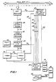
- FIG. 1 is a block diagram of a data processing printer system that incorporates the print engine data interface in accordance with this invention.
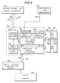
- FIG. 2 is a block diagram illustrating the principle components of the print engine data interface.
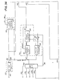
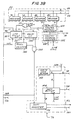
- FIGS. 3A through 3C when assembled, form a schematic diagram of the print engine data interface.
- FIG. 1 depicts in block diagram a print system 10 that is connected to a main processor (not illustrated) through a main bus 12 such as an ethernet line.
- the system is addressed through a host processor 14 that exercises control over the entire print system.
- a system bus 16 such as a Q-bus connects the system together.
- the host processor initially determines if the print system is being polled, or accessed, by the main processor. If it is determined that the print system is being accessed the host processor then determines whether the incoming packets of data are formatting data, called font data, or actual composition data. If the incoming data is font data it is passed through a horizontal line processor 20 to a font memory unit 22. If the data is composition data it is passed to an image generator processor 18.
- a direct memory access unit 24 serves as a high speed channel to transfer command and data signals to the image generator processor.
- the image generator processor responds to a particular packet of composition data by issuing an image command to the horizontal line processor 20.
- the horizontal line processor in response to the image command, and by reference to the font data generates a full page bit map address where a pixel should be produced.
- the bit map address is directed along a composition bus 26 to one of two full page bit maps (FPBM) 28 or 30 that the horizontal line processor selectively accesses.
- FPBM full page bit maps
- the pixel image is then stored in the full page bit map at the address the horizontal line processor generated.
- the full page bit map is fully loaded with pixels it is a representation of the page to be produced. This necessitates providing the full page bit maps 28, 30 with a very large amount of memory. In one embodiment of the invention, they are each a 1.25 megabyte array, and each bit within the array represents a potential pixel location.
- the full page bit map memories are connected to a print bus 32 that is connected to a print engine data interface (PDI) 34.
- the print engine data interface is connected to a print engine distribution board 36 that serves as the input-output interface for a print engine 38.
- the print engine controls the laser and other hardware elements necessary to produce a print document 39.
- the transmission of data through the print engine data interface is controlled by a printer control and status interface (PCSI) 40.
- the printer control and status interface is connected to the host processor by the Q-bus, to the print engine through the distribution board by a set of command and status lines 42 and to the print engine data interface by scan enable address, and data lines 44, 46 48 respectively, and to the full page bit map by assignment lines 49.
- the print engine transmits a line sync across a print engine line sync line 50 wherever it is ready to start a new scan line.
- the line sync line is connected to both the print engine data interface and the printer control and status interface.
- the printer control and status interface responds to the commands of the host processor 14 by starting and stopping the printer and by selecting the bus assignments of the full page bit map memories. It performs these functions by frequently polling the status of the printer and other elements of the system 10 and communicating their status to the host processor.
- the print engine data interface addresses the full page bit memory 28 or 30 that is to be accessed for printing, serially retrieves the pixel data contained therein, and forwards it to the print engine 38 for image processing.
- the print engine data interface also cyclically refreshes all the data stored in the full page bit memory. This keeps the data fresh and useable by the print engine when it would otherwise decay if the scan line is too short. This also makes it possible to repeatedly scan each full page bit map so multiple copies of the page may be produced without having to spend time re-composing the page each time.
- the print engine data interface 34 includes a set of command and data registers 52. These registers are designed to store page geometry parameters, specific to the type of print engine and page format the print engine data interface is being used, and print engine command data. These parameters are transferred by the printer control and status interface to the registers through PCSI address and PCSI data lines 46, 48. The PCSI scan enable command is also forwarded to these registers through the scan enable line 44. These parameters are referenced by a scan offset adjustments logic circuit 54 to adjust to the proper initial address at the beginning of each line scan.
- Reading, writing and refreshing of the full bit map memories are controlled by a refresh and read/write arbitration logic circuit 60.
- This circuit assigns the proper refresh or read/write commands to a bit map sequencer. This enables the bit map sequencer circuit to generate control signals to either refresh the data in the bit map for reading or retrieve it for transmission to the print engine.
- a bit map address counter 66 under command of the refresh and read/write arbitration circuit 60 and the bit map sequencer 62, is provided to point to the appropriate address in the full page bit map 28 or 30 so the correct data will be either refreshed or retrieved.
- the address is transmitted through a set of address lines 56.
- the retrieved data is read in byte form through a set of eight data lines 68 from the full page bit map.
- the data is transferred into a parallel-to-serial converter 70 where it is converted into a serial bit stream for transmission to the print engine distribution board through a data output line 162.
- the horizontal line processor 20 is connected to the print engine data interface through a refresh line 74, connected to the refresh and read/write arbitration logic. This refresh signal passed through this line is to synchronize the refresh timing when the bit map 28 or 30 accessed by the PDI is not being used to supply print commands to the print engine.
- the command and data registers 52 consist of four 8-bit registers 76, 78, 80, and 82 respectively and one D-type flip-flop 84, as shown in Fig. 3.
- the page parameters of the scan are assigned to the individual registers as follows: REGISTER DESCRIPTION Register 76 Bits 4-7 High 4 bits of scan offset adjustment Bit 3 Print Mode Select (H-Print; L- Print/Erase) Bit 2 Test-Enable PDI self-test mode Bits 0-1 High 2 bits of byte count per scan line Register 78 Bits 0-7 Lower 8 bits of scan offset adjustment Register 80 Bits 0-7 Lower 8 bits of byte count per scan line Register 82 Bits 0-7 Stored byte pattern to be written back to bit map during print/erase mode
- the registers are loaded with geometry parameters from the PCSI through the address and data lines 46 and 48 and the flip flop is triggered by a signal enable from the PCSI through the scan enable line 44.
- Flip flop 84 is used to generate a page enable signal along the page enable line 86 and is triggered by the line sync signal.
- the page enable is asserted during the entire frame of a page, is synchronous with the line sync, and thus is used as a system reference signal to enable data transfer.
- the scan offset adjustment circuit 54 consists of an offset adjust flip-flop 90, an offset counter 92 and a pulse stretcher 94.
- the scan line registration offset adjustment is made at the beginning of each scan line by loading one's complements of offset count from registers 76 and 78 into the offset counter 92 (connection not shown) and setting the offset adjust flip-flop.
- the offset adjust flip-flop enables the offset counter which counts engine clock pulses received through an engine clock line 96 as the scan progresses. When the total number of counts equals the count stored, the offset counter generates an offset reset signal on an offset reset line 98. The reset line is branched back to the offset adjust flip-flop so the offset adjust flip-flop 90 is reset.
- the pulse stretcher 94 along with an inverter 100 is used to load the offset counter at the beginning of the line with the scan value.
- the inverter 100 is used to invert the video clock signal from the print engine so sufficient time is provied to load the offset counter.
- a comparator can be used to detect the end of the offset, eliminating the need for the pulse stretcher.
- the bit map address counter 66 includes a line address counter 101, a column address counter 102 and a column address comparator 104. Each byte, or each image data unit, in the full page bit map is located by row address and column address. As the memory scan of the bit map progresses the line address counter is incremented by the rising edge of the line sync while at the same time the column address counter is incremented by an end R/W signal generated by the bit map sequencer and transmitted over an end R/W line 108. The addresses generated by the counters are transferred to one of the bit maps across the bit map address lines 56. This enables the sequential scanning of the bit map page during the read state.
- the number of data units to be read during each scan line is programmable, located in registers 76 and 78, enabling the PDI to adjust the scan through the scan offset adjust circuit 54 to accommodate paper of varying width.
- the column address comparator 104 detects the end address of each scan line by comparing it to the stored value from register 80. When the end of the scan line is reached the comparator resets a line status flip-flop 110. Since the length of the scan line is programmable it can be used to "image-clip" the length of a page.
- the bit map sequencer 62 consists of a memory synchronizer 112 and a sequencer 114.
- the sequencer 114 is a state machine that samples the input and the present state of the machine to determine its next state and output.
- the synchronizer is a clocked latch which is used to synchronize the sequencer input signals to prevent meta stable state transitions.
- the input to the synchronizer is from a refresh request line 116, a print/erase line 118 from register 76 (connection not shown), and a read/write request line 120.
- the output of the sequencer is two sets of control signals. One set is a set of bit map control signals, outputted along four bit map control lines 122 which are used to access and refresh the bit map.
- the second set of controls is internal to the PDI and includes the end read/write signal transmitted on the end read/write line 108, an end refresh signal transmitted on an end refresh line 124, an end memory access request signal transmitted on an end memory access line 126, and a write data enable signal asserted on a write data enable line 128.
- the arbitration logic unit 60 includes the line status flip-flop 110, a delay flip-flop 130, a multiplexer 132, an AND gate 134, a refresh request flip-flop 136 and a read/write request flip-flop 138.
- the multiplexer is a 2 to 1 unit that selects one of the refresher sources between either the horizontal line processor swap request through the horizontal line processor refresh line 74 or the burst refresh through a burst refresh line 140.
- the line status flip-flop registers the effective data period of the scan line. The output is transmitted along an inhibit refresh line 142 to the AND gate 134 and is used to inhibit refresh requests during implied refreshes.
- the line status flip-flop 110 may be reset by either the column address comparator 104 or by the line sync signal since they are gated together to the flip-flop through an OR gate 111.
- the complement of the line status flip-flop is used to activate a pixel counter 144 and the delay flip-flop 130.
- the output of the delay flip-flop 130 is in turn used to control the start of the memory cycle at each scan line. The delay is inserted to guarantee that the bit map sequencer 62 will always complete the current refresh cycle before any attempted memory scan, and that the scan adjustment between scan lines is uniform.
- the refresh request flip-flop 136 is asserted whenever a refresh request is received through refresh line 146 from the AND gate 124.
- the signal from the refresh request flip-flop is asserted along the refresh request line 116 to the bit map sequencer synchronizer 112.
- the read/write status flip-flop 138 is asserted when a memory access request is made by a read/write request NAND gate 150 through a read/write request line 148.
- the flip-flop 138 is reset at the end of the memory cycle by the end memory access signal from the sequencer 114 through the end memory access line 126.
- the output of this flip-flop is transmitted to the bit map sequencer synchronizer 112 through the read/write request line 120.
- the data conversion logic circuit includes a write data buffer 151, a data buffer 154 and a shift register 156. All three units have the same data width of one data unit.
- the circuit is synchronized by the pixel counter 144 and NAND gate 150 through the branch of the read/write request line 148. The synchronization is achieved when the pixel counter generates an output signal by counting the print engine clock to a data unit (connection now shown). The signal is further conditioned by logically ANDing the pixel count with that from the delay flip-flop 130 through the NAND gate 150. The resulting signal is a shift load signal triggering the loading of the data unit into the shift register 156 to start the read/write cycle.
- the data buffer 154 is used to synchronize the timing of the data transfer between the bit map memory and the print engine unit when the individual data units are transferred to the print engine.
- the data buffer is triggered by a read signal from the read/write sequencer through the read line 158.
- the write buffer 152 is a tri-state buffer which stores the data pattern to be written back to the bit map memory along the bit map data lines 68 when required by the print erase cycle.
- the buffer 152 is enabled by the write data enable signal asserted by the sequencer 114 through the write data enable line 128. During the scan process the retrieved data from the full page bit map 28 or 30 is first loaded temporarily into the data buffer 154 through the data lines 68.
- the data is then loaded into the shift register 156 and shifted out a bit at a time synchronously with the rising edge of the print engine clock.
- the print engine clock signal is transmitted to the shift register through a print engine clock line 162 and the data bits are transferred to the print engine through a video shift out line 160.
- the PDI also includes a 4 to 2 multiplexer 164 that selects the bit map synchronous signals from either the external print engine or from an internal data source.
- the multiplexer accepts either the print engine line sync through the print engine sync line 50 and the print signal engine clock through a print engine clock line 168, or signals from the PCSI through test enable and test clock lines 170, 172 respectively.
- the print engine line sync signal is passed through to the line sync line 88, and the print engine clock signal is passed through to a clock line 96, so as to synchronize the operation of the PDI.
- the PCSI test lines 170, 172 are provided so the PDI can do a self-test by writing a pattern into one of the bit maps and checking the content through the horizontal line processor without the presence of the print engine.
- a 20 MHz clock 174 is provided to run the bit map sequencer.
- the clock is converted directly to a prescaler 176 that derives a 10 MHz clock signal that is transferred to the multiplexer 164 through a test clock line 166 for the internal test, and a 1.25 MHz through the burst refresh line 140 to the refresh and read/write arbitration circuit 160 to provide a burst refresh signal.
- the bit map refresh is achieved by one of three stages of bit map refresh control.
- the first state synchronous refresh, occurs whenever the PDI has control of a full page bit map but that bit map is not being accessed by the print engine as a source of print command instructions.
- the refresh commands come from the horizontal line processor through refresh line 74.
- the second stage refresh is burst mode refresh. This occurs when the PDI is in the print mode.
- the refresh is synchronous with the internal 1.25 MHz reference clock.
- the burst mode refresh is inhibited during the effective bit map scan, or print engine read, period but remains active throughout the entire page scan period.
- the third state refresh is the implied refresh. This refresh takes advantage of the fact that each time a dynamic random access memory cell is accessed the entire row the memory cell is in can be refreshed. By sequentially accessing adjacent row addresses a memory refresh is achieved.
- the address bus of the PDI is arranged so that the output of the columns address counter is used to linearly address the rows of the bit map memory to achieve the refreshing.
- the line address counter is used to address columns of bit map memory.
- the burst mode refresh is provided because for some paper configurations the scan line width is too short so the entire full page bit map may not be refreshed during an implied refresh.
- the burst mode refresh periodically has the data refreshed so it will be useable by the print engine.
- one of the full page bit map memories is accessed by the PDI, it is able to both linearly retrieve the pixel data stored therein for transmission to the print engine, and to frequently have the data refreshed, so it remains useable.
- An advantage of this feature is that the bit map can be repeatedly accessed for printing multiple copies without having to spend time recomposing the page.
Abstract
Description
- This invention relates to printer engine drive units such as those adapted to transmit control signals to a print engine from a data processing system. In particular, it relates to a print engine drive interface unit for transmitting print command data from a dynamic memory to a print engine, and for refreshing the command data stored in the memory.
- Much work has been done in the recent years regarding the development of high-speed, high-quality data processing printers. A considerable fraction of this work has gone into the development of laser-type print engines. These print engines have a specially adapted laser with a beam that can be rapidly turned on and off to generate a raster type scan line composed of pixels, or dots, across a photoconductive surface. The adjacent scans of the laser beam are located within close proximity to each other so that when the surface is completely scanned a full, accurate depiction of the image to be produced is projected on the surface. A paper printout of the image may then be produced by conventional xerographic techniques.
- The advantage of using a laser-type print engine is that the pixel density can be quite high. A laser-type print engine can produce 90,000 or more pixels per square inch of output image. This makes it possible to produce figures and characters of extremely high quality, equal to those produced by much slower conventional printers with typewriter type impacting keys. Another advantage laser printers have over conventional printers is that they are not limited to printing only the figures contained on the type keys. The laser beam may be used to form a raster image of almost any combination of pixels desired. This is a desirable feature to have on a printer when printing either a business or technical document that includes irregularly shaped figures such as graph lines or scientific symbols.
- One problem with laser printing technology is that large amounts of print command data must be processed by the printing system at a very high rate of speed. This is because it is necessary for the printing system to almost simultaneously receive the output data from the processor to be printed, convert the data into pixel image form readable by the print engine, and transmit the pixel print commands in the appropriate sequence to the print engine so the laser will be activated at the appropriate times as its beam scans along the photoconductive surface.
- Thus, it is necessary to provide a data controller that can properly sequence the flow of data from the main processor, convert it to print engine-readable pixel form, and transmit the pixel data to the print engine.
- Currently, there are two approaches to data controller design. One approach uses a band buffer where a block of data is received by the controller, converted into pixel form, and stored in a buffer where it can be read by the print engine. A disadvantage of this system is the storage buffer is too small to store all of the pixel data necessary for some complex graph and symbol imagery. Thus, these controllers are of limited utility.
- In US-A-4031519 there is described a printer in which a page of data relating to information to be printed may be stored, and subsequent minor modifications to the information for that page may be made for subsequent copies to be printed.
- In IBM Technical Disclosure Bulletin,
Vol 24,No 2, July 1981 "Extended Graphics Storage and Serialization for Non-Impact Printers", T L Anderson et al there is described a printer with two line buffers for storing data to be printed, one line buffer being filled, while the other line buffer is being emptied. - Alternatively, the data controller may have a full page bit memory system. These controllers are provided with at least one full page bit memory map that is representative of the data to be retrieved and for scanning by the print engine. Processing circuitry within the data controller analyzes the input from the main processor to determine if it is either format data, called font data, or actual image composition data. An image generator circuit analyzes the composition data by referring to the font data, and produces a pixel representation of the image to be generated. The pixel output is loaded into the full page bit map memory. The print engine is able to access the full page bit map memory and reproduce on the photoconductive surface the image stored therein. This makes it possible to generate a full page of print output with graphs and other complex figures represented thereon.
- Full page bit memory controllers can be rather slow devices because it has proved very difficult to transmit data to one position of the full page bit map and to send data from another section of the bit map at the same time. Also, some image generating systems do not transmit data to the bit map serially. With these systems the engine bit map must be fully composed before it is ready to be accessed by the print engine. If only one bit map is provided, it is necessary to follow a pattern of first loading it with pixel data, and then having the print engine access it. This slows down the operation of both the image generator and the print engine since one must remain idle while the other has access to the bit map. Therefore, it is desirable to provide the data controller with at least two full page bit maps so one may be accessed by the image processor while the other is accessed by the print engine.
- Another disadvantage of full page bit memory systems is that they have memory elements that usually need to be refreshed. This is because the typical full page bit memory is a dynamic memory, meaning that the electrical charges in it that represents the data tends to decay over time. This is a problem because data stored early within the print engine will decay and become unuseable before it is accessed by the print engine. Also this decay makes it almost impossible for the print engine to repeatedly access a bit map thereon or so that multiple copies of the page represented thereon can be printed.
- A need therefore exists for a means to control the print engine's access to the bit memory system. The print engine should have access to at least two full page bit map memories so it can have access to one while the image generator has access to the other. Also, there should be a means to access the full page maps so data stored therein is frequently refreshed so as to prevent it from decaying and becoming unreadable.
- The invention is defined in the single claim.
- The invention comprises providing a print engine data interface circuit that can be selectively connected to one of a number of full page bit maps that provide the print engine with pixel data. The print engine data interface is designed to access one of the full page bit maps and serially transmit the pixel data contained therein to the print engine. Thus, when two full page bit maps are provided, it is possible to dedicate one of the full page bit maps to the print engine while the other is being loaded with data from the image processor. Both the image processor and the print engine can thus be operated at maximum efficiency in order to generate hard paper copies as fast as possible.
- Also, the print engine of this invention is designed to frequently refresh the data stored in the full page bit map it has access to. This keeps the data within the memories in an optimal condition so the full page bit map may be repeatedly accessed by the print engine to provide multiple copies of the same output.
- The print engine drive interface is connected to the print engine, a print bus, and a printer control and status interface. The print bus is connected to at least two full page bit maps The printer control and status interface is connected to both the print engine data interface and the full page bit map memories. It controls the bit map assignments for both the reading to the bit map from the image processor and the access to a bit map by the print engine data interface. The printer control and status interface also directs page geometry parameters to the print engine data interface. The printer control and status interface transmits these control signals in response to initial page parameters supplied to it in the terms of formatting information, and in response to status signals generated by the print engine.
- The print engine drive interface includes a set of command and data registers for storing the page geometry parameters transmitted from the printer control and status interface. A scan offset adjustment circuit uses the parameters in the command and data registers to synchronize the retrieval of the pixel data from the full page bit map so that it is synchronous with the demand from the print engine, and to control the length of the memory scan of the memory so it is of an appropriate length to be acceptable with the print engine's requirement for print command data. A bit map sequencer is designed to generate either read/write or refresh control signals to the bit map memory while it is controlled by the print engine data interface. This provides command signals so the memory rows with the full page bit memory are either read or refreshed. The bit map sequencer is controlled by a refresh and read/write arbitration logic circuit.
- The print engine drive interface is also provided with a bit map address control circuit for generating a current data address so the correct data can be retrieved by the bit map sequencer. The retrieved data is read into a parallel to serial data conversion unit for transmission to the print engine.
- FIG. 1 is a block diagram of a data processing printer system that incorporates the print engine data interface in accordance with this invention.
- FIG. 2 is a block diagram illustrating the principle components of the print engine data interface.
- FIGS. 3A through 3C, when assembled, form a schematic diagram of the print engine data interface.
- FIG. 1 depicts in block diagram a print system 10 that is connected to a main processor (not illustrated) through a main bus 12 such as an ethernet line. The system is addressed through a
host processor 14 that exercises control over the entire print system. A system bus 16 such as a Q-bus connects the system together. The host processor initially determines if the print system is being polled, or accessed, by the main processor. If it is determined that the print system is being accessed the host processor then determines whether the incoming packets of data are formatting data, called font data, or actual composition data. If the incoming data is font data it is passed through ahorizontal line processor 20 to afont memory unit 22. If the data is composition data it is passed to animage generator processor 18. A directmemory access unit 24 serves as a high speed channel to transfer command and data signals to the image generator processor. - The image generator processor responds to a particular packet of composition data by issuing an image command to the
horizontal line processor 20. The horizontal line processor in response to the image command, and by reference to the font data generates a full page bit map address where a pixel should be produced. The bit map address is directed along acomposition bus 26 to one of two full page bit maps (FPBM) 28 or 30 that the horizontal line processor selectively accesses. The pixel image is then stored in the full page bit map at the address the horizontal line processor generated. When the full page bit map is fully loaded with pixels it is a representation of the page to be produced. This necessitates providing the full page bit maps 28, 30 with a very large amount of memory. In one embodiment of the invention, they are each a 1.25 megabyte array, and each bit within the array represents a potential pixel location. - The full page bit map memories are connected to a
print bus 32 that is connected to a print engine data interface (PDI) 34. The print engine data interface is connected to a printengine distribution board 36 that serves as the input-output interface for aprint engine 38. The print engine controls the laser and other hardware elements necessary to produce aprint document 39. - The transmission of data through the print engine data interface is controlled by a printer control and status interface (PCSI) 40. The printer control and status interface is connected to the host processor by the Q-bus, to the print engine through the distribution board by a set of command and
status lines 42 and to the print engine data interface by scan enable address, anddata lines line sync line 50 wherever it is ready to start a new scan line. The line sync line is connected to both the print engine data interface and the printer control and status interface. The printer control and status interface responds to the commands of thehost processor 14 by starting and stopping the printer and by selecting the bus assignments of the full page bit map memories. It performs these functions by frequently polling the status of the printer and other elements of the system 10 and communicating their status to the host processor. - The print engine data interface addresses the full
page bit memory print engine 38 for image processing. The print engine data interface also cyclically refreshes all the data stored in the full page bit memory. This keeps the data fresh and useable by the print engine when it would otherwise decay if the scan line is too short. This also makes it possible to repeatedly scan each full page bit map so multiple copies of the page may be produced without having to spend time re-composing the page each time. - Referring now to FIG. 2 it is seen that the print
engine data interface 34 includes a set of command and data registers 52. These registers are designed to store page geometry parameters, specific to the type of print engine and page format the print engine data interface is being used, and print engine command data. These parameters are transferred by the printer control and status interface to the registers through PCSI address and PCSI data lines 46, 48. The PCSI scan enable command is also forwarded to these registers through the scan enableline 44. These parameters are referenced by a scan offsetadjustments logic circuit 54 to adjust to the proper initial address at the beginning of each line scan. - Reading, writing and refreshing of the full bit map memories are controlled by a refresh and read/write
arbitration logic circuit 60. This circuit assigns the proper refresh or read/write commands to a bit map sequencer. This enables the bit map sequencer circuit to generate control signals to either refresh the data in the bit map for reading or retrieve it for transmission to the print engine. - A bit
map address counter 66 under command of the refresh and read/write arbitration circuit 60 and thebit map sequencer 62, is provided to point to the appropriate address in the fullpage bit map data lines 68 from the full page bit map. The data is transferred into a parallel-to-serial converter 70 where it is converted into a serial bit stream for transmission to the print engine distribution board through adata output line 162. - The
horizontal line processor 20 is connected to the print engine data interface through arefresh line 74, connected to the refresh and read/write arbitration logic. This refresh signal passed through this line is to synchronize the refresh timing when thebit map REGISTER DESCRIPTION Register 76 Bits 4-7 High 4 bits of scan offset adjustmentBit 3 Print Mode Select (H-Print; L- Print/Erase) Bit 2Test-Enable PDI self-test mode Bits 0-1 High 2 bits of byte count per scan lineRegister 78 Bits 0-7 Lower 8 bits of scan offsetadjustment Register 80 Bits 0-7 Lower 8 bits of byte count perscan line Register 82 Bits 0-7 Stored byte pattern to be written back to bit map during print/erase mode - The registers are loaded with geometry parameters from the PCSI through the address and
data lines line 44. Flip flop 84 is used to generate a page enable signal along the page enable line 86 and is triggered by the line sync signal. The page enable is asserted during the entire frame of a page, is synchronous with the line sync, and thus is used as a system reference signal to enable data transfer. - The scan offset
adjustment circuit 54 consists of an offset adjust flip-flop 90, an offsetcounter 92 and apulse stretcher 94. The scan line registration offset adjustment is made at the beginning of each scan line by loading one's complements of offset count fromregisters 76 and 78 into the offset counter 92 (connection not shown) and setting the offset adjust flip-flop. The offset adjust flip-flop enables the offset counter which counts engine clock pulses received through anengine clock line 96 as the scan progresses. When the total number of counts equals the count stored, the offset counter generates an offset reset signal on an offsetreset line 98. The reset line is branched back to the offset adjust flip-flop so the offset adjust flip-flop 90 is reset. Thepulse stretcher 94 along with aninverter 100 is used to load the offset counter at the beginning of the line with the scan value. Theinverter 100 is used to invert the video clock signal from the print engine so sufficient time is provied to load the offset counter. Alternatively, a comparator can be used to detect the end of the offset, eliminating the need for the pulse stretcher. - The bit
map address counter 66 includes a line address counter 101, acolumn address counter 102 and acolumn address comparator 104. Each byte, or each image data unit, in the full page bit map is located by row address and column address. As the memory scan of the bit map progresses the line address counter is incremented by the rising edge of the line sync while at the same time the column address counter is incremented by an end R/W signal generated by the bit map sequencer and transmitted over an end R/W line 108. The addresses generated by the counters are transferred to one of the bit maps across the bit map address lines 56. This enables the sequential scanning of the bit map page during the read state. The number of data units to be read during each scan line is programmable, located inregisters 76 and 78, enabling the PDI to adjust the scan through the scan offset adjustcircuit 54 to accommodate paper of varying width. Thecolumn address comparator 104 detects the end address of each scan line by comparing it to the stored value fromregister 80. When the end of the scan line is reached the comparator resets a line status flip-flop 110. Since the length of the scan line is programmable it can be used to "image-clip" the length of a page. - The
bit map sequencer 62 consists of a memory synchronizer 112 and asequencer 114. Thesequencer 114 is a state machine that samples the input and the present state of the machine to determine its next state and output. The synchronizer is a clocked latch which is used to synchronize the sequencer input signals to prevent meta stable state transitions. The input to the synchronizer is from arefresh request line 116, a print/eraseline 118 from register 76 (connection not shown), and a read/write request line 120. The output of the sequencer is two sets of control signals. One set is a set of bit map control signals, outputted along four bitmap control lines 122 which are used to access and refresh the bit map. The second set of controls is internal to the PDI and includes the end read/write signal transmitted on the end read/write line 108, an end refresh signal transmitted on anend refresh line 124, an end memory access request signal transmitted on an endmemory access line 126, and a write data enable signal asserted on a write data enableline 128. - The
arbitration logic unit 60 includes the line status flip-flop 110, a delay flip-flop 130, amultiplexer 132, an ANDgate 134, a refresh request flip-flop 136 and a read/write request flip-flop 138. The multiplexer is a 2 to 1 unit that selects one of the refresher sources between either the horizontal line processor swap request through the horizontal lineprocessor refresh line 74 or the burst refresh through aburst refresh line 140. The line status flip-flop registers the effective data period of the scan line. The output is transmitted along an inhibitrefresh line 142 to the ANDgate 134 and is used to inhibit refresh requests during implied refreshes. The line status flip-flop 110 may be reset by either thecolumn address comparator 104 or by the line sync signal since they are gated together to the flip-flop through an OR gate 111. The complement of the line status flip-flop is used to activate apixel counter 144 and the delay flip-flop 130. The output of the delay flip-flop 130 is in turn used to control the start of the memory cycle at each scan line. The delay is inserted to guarantee that thebit map sequencer 62 will always complete the current refresh cycle before any attempted memory scan, and that the scan adjustment between scan lines is uniform. - The refresh request flip-
flop 136 is asserted whenever a refresh request is received throughrefresh line 146 from the ANDgate 124. The signal from the refresh request flip-flop is asserted along therefresh request line 116 to the bit map sequencer synchronizer 112. The read/write status flip-flop 138 is asserted when a memory access request is made by a read/writerequest NAND gate 150 through a read/write request line 148. The flip-flop 138 is reset at the end of the memory cycle by the end memory access signal from thesequencer 114 through the endmemory access line 126. The output of this flip-flop is transmitted to the bit map sequencer synchronizer 112 through the read/write request line 120. - The data conversion logic circuit includes a write data buffer 151, a
data buffer 154 and ashift register 156. All three units have the same data width of one data unit. The circuit is synchronized by thepixel counter 144 andNAND gate 150 through the branch of the read/write request line 148. The synchronization is achieved when the pixel counter generates an output signal by counting the print engine clock to a data unit (connection now shown). The signal is further conditioned by logically ANDing the pixel count with that from the delay flip-flop 130 through theNAND gate 150. The resulting signal is a shift load signal triggering the loading of the data unit into theshift register 156 to start the read/write cycle. Thedata buffer 154 is used to synchronize the timing of the data transfer between the bit map memory and the print engine unit when the individual data units are transferred to the print engine. The data buffer is triggered by a read signal from the read/write sequencer through the readline 158. Thewrite buffer 152 is a tri-state buffer which stores the data pattern to be written back to the bit map memory along the bit map data lines 68 when required by the print erase cycle. Thebuffer 152 is enabled by the write data enable signal asserted by thesequencer 114 through the write data enableline 128. During the scan process the retrieved data from the fullpage bit map data buffer 154 through the data lines 68. The data is then loaded into theshift register 156 and shifted out a bit at a time synchronously with the rising edge of the print engine clock. The print engine clock signal is transmitted to the shift register through a printengine clock line 162 and the data bits are transferred to the print engine through a video shift outline 160. - The PDI also includes a 4 to 2
multiplexer 164 that selects the bit map synchronous signals from either the external print engine or from an internal data source. In this embodiment of the invention the multiplexer accepts either the print engine line sync through the printengine sync line 50 and the print signal engine clock through a printengine clock line 168, or signals from the PCSI through test enable andtest clock lines line sync line 88, and the print engine clock signal is passed through to aclock line 96, so as to synchronize the operation of the PDI. ThePCSI test lines - A 20
MHz clock 174 is provided to run the bit map sequencer. The clock is converted directly to aprescaler 176 that derives a 10 MHz clock signal that is transferred to themultiplexer 164 through atest clock line 166 for the internal test, and a 1.25 MHz through theburst refresh line 140 to the refresh and read/write arbitration circuit 160 to provide a burst refresh signal. - The bit map refresh is achieved by one of three stages of bit map refresh control. The first state, synchronous refresh, occurs whenever the PDI has control of a full page bit map but that bit map is not being accessed by the print engine as a source of print command instructions. In this stage, the refresh commands come from the horizontal line processor through
refresh line 74. The second stage refresh is burst mode refresh. This occurs when the PDI is in the print mode. The refresh is synchronous with the internal 1.25 MHz reference clock. The burst mode refresh is inhibited during the effective bit map scan, or print engine read, period but remains active throughout the entire page scan period. - The third state refresh is the implied refresh. This refresh takes advantage of the fact that each time a dynamic random access memory cell is accessed the entire row the memory cell is in can be refreshed. By sequentially accessing adjacent row addresses a memory refresh is achieved. The address bus of the PDI is arranged so that the output of the columns address counter is used to linearly address the rows of the bit map memory to achieve the refreshing. The line address counter is used to address columns of bit map memory.
- The burst mode refresh is provided because for some paper configurations the scan line width is too short so the entire full page bit map may not be refreshed during an implied refresh. The burst mode refresh periodically has the data refreshed so it will be useable by the print engine. Thus, when one of the full page bit map memories is accessed by the PDI, it is able to both linearly retrieve the pixel data stored therein for transmission to the print engine, and to frequently have the data refreshed, so it remains useable. An advantage of this feature is that the bit map can be repeatedly accessed for printing multiple copies without having to spend time recomposing the page.
- It is understood that this description is for the purposes of illustration. Therefore it is intended that all matter contained in the above description or shown in the accompanying drawings be interpreted as illustrative and not limiting.
Claims (1)
- A system comprising:
a print engine,
a printer control and status interface (40), and
a print engine data interface capable of reading pixel image data from a full page bit map memory and serially transferring the read data to a print engine (38) in response to signals from a horizontal line processor (20), said print engine data interface including:a) a set of command and data registers (52) for storing programmed page format and scan length data from said printer control and status interface (40), andb) a scan offset adjustment circuit (54) coupled to receive the page format and scan length data from the command and data registers (52)
characterized in that said system includes a plurality of full page bit map memories (28,30) coupled to said print engine data interface, and wherein the print engine data interface further comprises:c) means (174) for periodically generating a burst refresh signal;d) an arbitration circuit (60) coupled to detect whether each of said plurality of full page bit map memories (28,30) is to be read from, written to, or refreshed, said arbitration circuit (60) outputting refresh request signals in response to burst refresh signals to start the refresh cycle and outputting read/write request signals to start the memory cycle of each scan line;e) a bit map sequencer (62) coupled to said arbitration circuit (60) for generating read/write or refresh control signals for controlling each of said plurality of bit map memories (28,30) in dependence on the request signals output by said arbitration circuit (60);f) a bit map memory address counter (66) coupled to said bit map sequencer (62) and to said command and data registers (52) for addressing each of said plurality of full page bit map memories (28,30); andg) a data conversion circuit (70) coupled to receive data retrieved in parallel from each of said plurality of bit map memories (28,30) and converting the parallel data into a serial data stream for synchronous reception by the print engine (38) in response to an enabling signal from said arbitration circuit (60),whereby the pixel image data stored in each one of said plurality of bit map memories (28,30) is periodically refreshed in response to said burst refresh signals when said print engine data interface (34) is in the print mode.
Applications Claiming Priority (2)
| Application Number | Priority Date | Filing Date | Title |
|---|---|---|---|
| US900057 | 1986-08-25 | ||
| US06/900,057 US4809216A (en) | 1986-08-25 | 1986-08-25 | Print engine data interface |
Publications (2)
| Publication Number | Publication Date |
|---|---|
| EP0321491A1 EP0321491A1 (en) | 1989-06-28 |
| EP0321491B1 true EP0321491B1 (en) | 1993-06-16 |
Family
ID=25411916
Family Applications (1)
| Application Number | Title | Priority Date | Filing Date |
|---|---|---|---|
| EP87905879A Expired - Lifetime EP0321491B1 (en) | 1986-08-25 | 1987-08-25 | Print engine drive interface |
Country Status (8)
| Country | Link |
|---|---|
| US (1) | US4809216A (en) |
| EP (1) | EP0321491B1 (en) |
| JP (1) | JPH01502142A (en) |
| KR (1) | KR950010901B1 (en) |
| AU (1) | AU609737B2 (en) |
| CA (1) | CA1286418C (en) |
| DE (1) | DE3786269T2 (en) |
| WO (1) | WO1988001768A1 (en) |
Families Citing this family (24)
| Publication number | Priority date | Publication date | Assignee | Title |
|---|---|---|---|---|
| US4992956A (en) * | 1987-10-08 | 1991-02-12 | Advanced Micro Devices, Inc. | Apparatus for assembling data for supply to a scanning output device |
| US4894805A (en) * | 1988-04-28 | 1990-01-16 | Eastman Kodak Company | Security printer/copier |
| CA1327851C (en) * | 1988-06-22 | 1994-03-15 | Amy S. Christopher | Reconfigurable printer |
| US5167020A (en) * | 1989-05-25 | 1992-11-24 | The Boeing Company | Serial data transmitter with dual buffers operating separately and having scan and self test modes |
| US5121146A (en) * | 1989-12-27 | 1992-06-09 | Am International, Inc. | Imaging diode array and system |
| US5819014A (en) * | 1990-04-06 | 1998-10-06 | Digital Equipment Corporation | Parallel distributed printer controller architecture |
| JPH0535442A (en) * | 1991-07-31 | 1993-02-12 | Toshiba Corp | Image data converting circuit |
| JPH0779404B2 (en) * | 1991-08-16 | 1995-08-23 | ヒュンダイ エレクトロニクス インダストリーズ カムパニー リミテッド | Data transmission device for high density thermal recording head |
| US5511152A (en) * | 1993-09-20 | 1996-04-23 | Digital Equipment Corporation | Memory subsystem for bitmap printer data controller |
| JPH08174921A (en) * | 1994-12-22 | 1996-07-09 | Hitachi Koki Co Ltd | Apparatus for controlling page printer |
| US6657741B1 (en) * | 1995-08-07 | 2003-12-02 | Tr Systems, Inc. | Multiple print engine system with selectively distributed ripped pages |
| US7046391B1 (en) * | 1995-08-07 | 2006-05-16 | Electronics For Imaging, Inc. | Method and apparatus for providing a color-balanced multiple print engine |
| US6977752B1 (en) * | 1995-08-07 | 2005-12-20 | Electronics For Imaging, Inc. | Method and apparatus for determining toner level in electrophotographic print engines |
| EP0769755B1 (en) * | 1995-10-13 | 2003-04-09 | Seiko Epson Corporation | Apparatus and method for printing partially repetitive data |
| KR0155082B1 (en) * | 1996-03-29 | 1998-12-01 | 김광호 | Data conversion method of printer driver |
| US5835788A (en) * | 1996-09-18 | 1998-11-10 | Electronics For Imaging | System for transferring input/output data independently through an input/output bus interface in response to programmable instructions stored in a program memory |
| JP3498549B2 (en) * | 1997-10-03 | 2004-02-16 | ミノルタ株式会社 | Copying system and printer |
| US6625331B1 (en) * | 1998-07-03 | 2003-09-23 | Minolta Co., Ltd. | Image forming apparatus |
| US6356355B1 (en) | 1998-09-30 | 2002-03-12 | International Business Machines Corporation | Method and apparatus in a data processing system for generating metadata streams with per page data |
| US6295538B1 (en) | 1998-12-03 | 2001-09-25 | International Business Machines Corporation | Method and apparatus for creating metadata streams with embedded device information |
| US7551298B2 (en) * | 2004-06-04 | 2009-06-23 | Primax Electronics Ltd. | Print control device with embedded engine simulation module and test method thereof |
| US8947734B1 (en) * | 2006-07-27 | 2015-02-03 | Marvell International Ltd. | Pulse width modulator for a printing device |
| DE202010012884U1 (en) | 2010-11-15 | 2011-02-17 | Hüttinger Elektronik GmbH & Co.KG | Power generator arrangement |
| JP2023048386A (en) * | 2021-09-28 | 2023-04-07 | キヤノン株式会社 | Image forming device and control method of image forming device |
Family Cites Families (12)
| Publication number | Priority date | Publication date | Assignee | Title |
|---|---|---|---|---|
| AR245836A1 (en) * | 1974-11-11 | 1994-02-28 | Ibm | Printing system |
| US4074254A (en) * | 1976-07-22 | 1978-02-14 | International Business Machines Corporation | Xy addressable and updateable compressed video refresh buffer for digital tv display |
| US4300206A (en) * | 1977-06-30 | 1981-11-10 | International Business Machines Corporation | Flexible text and image generator for a raster printer |
| US4203154A (en) * | 1978-04-24 | 1980-05-13 | Xerox Corporation | Electronic image processing system |
| US4590585A (en) * | 1982-08-13 | 1986-05-20 | International Business Machines | Character generator for raster printer |
| US4649513A (en) * | 1983-11-15 | 1987-03-10 | International Business Machines Corporation | Apparatus and method for processing system printing data records on a page printer |
| JPS60107796A (en) * | 1983-11-16 | 1985-06-13 | Sony Corp | Control circuit of dynamic memory |
| JPS61131119A (en) * | 1984-11-30 | 1986-06-18 | Toshiba Corp | Page memory managing system |
| US4601018A (en) * | 1985-01-29 | 1986-07-15 | Allen Baum | Banked memory circuit |
| US4651278A (en) * | 1985-02-11 | 1987-03-17 | International Business Machines Corporation | Interface process for an all points addressable printer |
| US4648032A (en) * | 1985-02-13 | 1987-03-03 | International Business Machines Corporation | Dual purpose screen/memory refresh counter |
| NL8502641A (en) * | 1985-09-27 | 1986-04-01 | Oce Nederland Bv | GRID IMAGE MEMORY. |
-
1986
- 1986-08-25 US US06/900,057 patent/US4809216A/en not_active Expired - Lifetime
-
1987
- 1987-08-25 AU AU78774/87A patent/AU609737B2/en not_active Ceased
- 1987-08-25 WO PCT/US1987/002128 patent/WO1988001768A1/en active IP Right Grant
- 1987-08-25 CA CA000545280A patent/CA1286418C/en not_active Expired - Fee Related
- 1987-08-25 JP JP62505477A patent/JPH01502142A/en active Pending
- 1987-08-25 DE DE87905879T patent/DE3786269T2/en not_active Expired - Lifetime
- 1987-08-25 EP EP87905879A patent/EP0321491B1/en not_active Expired - Lifetime
- 1987-08-25 KR KR1019880700444A patent/KR950010901B1/en active IP Right Grant
Also Published As
| Publication number | Publication date |
|---|---|
| AU7877487A (en) | 1988-03-24 |
| JPH01502142A (en) | 1989-07-27 |
| EP0321491A1 (en) | 1989-06-28 |
| CA1286418C (en) | 1991-07-16 |
| US4809216A (en) | 1989-02-28 |
| WO1988001768A1 (en) | 1988-03-10 |
| DE3786269T2 (en) | 1994-01-20 |
| DE3786269D1 (en) | 1993-07-22 |
| AU609737B2 (en) | 1991-05-09 |
| KR880701915A (en) | 1988-11-07 |
| KR950010901B1 (en) | 1995-09-25 |
Similar Documents
| Publication | Publication Date | Title |
|---|---|---|
| EP0321491B1 (en) | Print engine drive interface | |
| US4486856A (en) | Cache memory and control circuit | |
| US4467448A (en) | Image rotate control circuitry | |
| GB1586589A (en) | Printing systems | |
| US5408539A (en) | Tessellating and quadding pels during image transfer | |
| US5163123A (en) | Synchronously transferring image data to a printer | |
| US5347617A (en) | Printer having a multiple scan line printhead controller | |
| US5043918A (en) | Multiple bus image controller structure for color page printers | |
| JPH01129291A (en) | Front end apparatus for raster output scanner | |
| US5467437A (en) | Recording apparatus | |
| US4703438A (en) | Character signal generator | |
| JPS60124764A (en) | Direct memory access controller | |
| GB2185608A (en) | Laser printer control system | |
| US5067097A (en) | Image memory controller | |
| JPS635768B2 (en) | ||
| US5341471A (en) | Controller for accessing an image data memory based on a state of a hard copy printer | |
| JPH08142409A (en) | Printer | |
| JPH0645252B2 (en) | Rastaskian printer controller | |
| KR100228788B1 (en) | Dynamic structure method and circuit of memory in color printing system | |
| JP4730474B2 (en) | Image processing device | |
| JP2922660B2 (en) | Image processing device | |
| JP2001134484A (en) | Method and device for controlling memory | |
| JPS61106262A (en) | Printer | |
| JPH047966A (en) | Printer controller | |
| JPS60245362A (en) | Printer control device |
Legal Events
| Date | Code | Title | Description |
|---|---|---|---|
| PUAI | Public reference made under article 153(3) epc to a published international application that has entered the european phase |
Free format text: ORIGINAL CODE: 0009012 |
|
| 17P | Request for examination filed |
Effective date: 19890215 |
|
| AK | Designated contracting states |
Kind code of ref document: A1 Designated state(s): DE FR GB |
|
| 17Q | First examination report despatched |
Effective date: 19910614 |
|
| GRAA | (expected) grant |
Free format text: ORIGINAL CODE: 0009210 |
|
| AK | Designated contracting states |
Kind code of ref document: B1 Designated state(s): DE FR GB |
|
| REF | Corresponds to: |
Ref document number: 3786269 Country of ref document: DE Date of ref document: 19930722 |
|
| ET | Fr: translation filed | ||
| PLBE | No opposition filed within time limit |
Free format text: ORIGINAL CODE: 0009261 |
|
| STAA | Information on the status of an ep patent application or granted ep patent |
Free format text: STATUS: NO OPPOSITION FILED WITHIN TIME LIMIT |
|
| 26N | No opposition filed | ||
| REG | Reference to a national code |
Ref country code: GB Ref legal event code: 732E |
|
| REG | Reference to a national code |
Ref country code: GB Ref legal event code: IF02 |
|
| REG | Reference to a national code |
Ref country code: GB Ref legal event code: 732E |
|
| PGFP | Annual fee paid to national office [announced via postgrant information from national office to epo] |
Ref country code: GB Payment date: 20060825 Year of fee payment: 20 |
|
| PGFP | Annual fee paid to national office [announced via postgrant information from national office to epo] |
Ref country code: FR Payment date: 20060831 Year of fee payment: 20 |
|
| PGFP | Annual fee paid to national office [announced via postgrant information from national office to epo] |
Ref country code: DE Payment date: 20061002 Year of fee payment: 20 |
|
| REG | Reference to a national code |
Ref country code: GB Ref legal event code: PE20 |
|
| PG25 | Lapsed in a contracting state [announced via postgrant information from national office to epo] |
Ref country code: GB Free format text: LAPSE BECAUSE OF EXPIRATION OF PROTECTION Effective date: 20070824 |