EP0327112A2 - Method and apparatus for displaying picture frames of color photograhic films - Google Patents
Method and apparatus for displaying picture frames of color photograhic films Download PDFInfo
- Publication number
- EP0327112A2 EP0327112A2 EP89101935A EP89101935A EP0327112A2 EP 0327112 A2 EP0327112 A2 EP 0327112A2 EP 89101935 A EP89101935 A EP 89101935A EP 89101935 A EP89101935 A EP 89101935A EP 0327112 A2 EP0327112 A2 EP 0327112A2
- Authority
- EP
- European Patent Office
- Prior art keywords
- image
- picture frame
- image data
- pixels
- size
- Prior art date
- Legal status (The legal status is an assumption and is not a legal conclusion. Google has not performed a legal analysis and makes no representation as to the accuracy of the status listed.)
- Granted
Links
Images


Classifications
-
- H—ELECTRICITY
- H04—ELECTRIC COMMUNICATION TECHNIQUE
- H04N—PICTORIAL COMMUNICATION, e.g. TELEVISION
- H04N1/00—Scanning, transmission or reproduction of documents or the like, e.g. facsimile transmission; Details thereof
- H04N1/387—Composing, repositioning or otherwise geometrically modifying originals
- H04N1/393—Enlarging or reducing
- H04N1/3935—Enlarging or reducing with modification of image resolution, i.e. determining the values of picture elements at new relative positions
Abstract
Description
- The present invention relates to a method and apparatus for displaying, on an image display unit, picture frames of color photographic films taken with a television camera. More particularly, the present invention relates to a method and apparatus for displaying picture frames of various sizes at the same dimension on an image display unit, by thinning pixels based on the size of a frame and writing the thinned image data in an image memory.
- A video type color film analyzer estimates the quality of a color image within a picture frame of a color photographic film using an image display system, prior to printing it out. Each picture frame of a color photographic film is taken with a television camera (hereinafter called TV camera), and the image data of pixels are stored in an image memory. The image data read out from the image memory are subjected to various image processings and thereafter, displayed on an image display unit such as a color CRT in the form of a color positive image. An operator checks the image displayed on the color CRT if a finished print thereof becomes fine or not. If not, the operator empirically determines exposure correction data according to which the exposure light amount is set and the picture frame is printed.
- According to known display arrangements of picture frames, a plurality of color CRTs are arranged in a line to display one color picture image per one color CRT as disclosed, e.g., in Japanese Patent Laid-open Publication No.62-141530, or a plurality of color picture images are displayed in a matrix pattern on one color CRT as disclosed, e.g., in European Unexamined Patent Publication No.0108158.
- The TV camera of the above-mentioned known color film analyzer has its optical magnification factor adjusted such that a full size of a color picture image of a 135 type photographic film (35 mm photographic film within a patrone) is displayed on the whole effective display or image pickup area. Such a fixed magnification factor has been used because most of amateurs use 135 type photographic films (hereinafter simply called "135 F"). As a result, if a 135 type half size color photographic film (hereinafter simply called "135 H") or a 110 type color photographic film (hereinafter simply called "110 type"), both having the frame size smaller than 135 F, is used, the image of a color picture frame is displayed in reduced size on the color CRT, resulting in a difficulty of inspecting a color image, inefficient use of the image memory and effective display area of the color CRT.
- Adjusting an image size (changing a magnification) is generally performed by means of an optical system such as a zoom lens. Such an optical magnification change necessiates to use a zoom lens, pulse motor, lens position detector and the like, resulting in poor cost effectiveness in spite of the fact that color photographic films are standardized in size and the number of types is small.
-
- It it therefore an object of the present invention to provide a method and apparatus for displaying picture frames of a color photographic film at the same dimension on an image display unit, by electrically performing magnification change when writing picture image data in an image memory.
- The above and other objects and advantages of the present invention can be achieved by the following manner: A picture frame of a color photographic film is taken with a TV camera. The image data of pixels of the picture frame are stored in an image memory such that all the pixels within the predetermined portion of the image pickup area of the TV camera are stored for a picture image small in size, whereas the pixels are thinned one pixel out of a predetermined number of pixels for a picture image large in size.
- Almost all of photographic films brought in laboratories are "135 F", "135 H" and "110 type". According to a preferred embodiment of this invention, all the pixel image data within a predetermined portion of the image pickup area are stored in an image data for "110 type", whereas the pixels within the image pickup area are thinned one pixel out of a predetermined number of pixels for "135 F" and the thinned image data are stored. For "135 H", the pixels are thinned one pixel out of a predetermined number of pixels in the vertical direction, and the picture frame is rotated by 90 degrees by interchanging the horizontal and vertical addresses and the resultant pixel image data are stored.
- The more the pixels are thinned, the more the resolution of a color image displayed on an image display unit deteriorates. To suppress lowering the resolution and to use the same number of pixels for both 135 type and 110 type films the latter being next popularly used, it is preferable to thin pixels by "1/2" for "135 F" and "135 H". It is also preferable that the pixel image data of a picture frame for "135 H" thinned in the vertical direction are temporarily stored in a buffer memory and thereafter, the addresses are interchanged between the horizontal and vertical directions to read the pixel image data from the buffer memory and store the read-out image data in an image memory.
- According to the present invention, the magnification change is electrically performed such that the same number of pixels are stored for each of picture frames different in size. Therefore, the magnification change can be conducted readily to display a picture frame different in size at the same dimension on an image display unit. In addition, it becomes possible to efficiently use the image memory and image display unit.
- The objects of the present invention will be seen by reference to the following detailed description, taken in connection with the accompanying drawings, in which:
- Fig.1 is a schematic diagram showing an embodiment of a color film analyzer according to the present invention;
- Fig.2 is a block diagram showing an example of the image processing unit shown in Fig.1;
- Fig.3 is a view used for explaining the relationship between the image pickup area and picture frame sizes;
- Figs.4A to 4C illustrate the pixels for "135 F", "135 H" and "110 type" picture frames written in image memories;
- Fig.5 is a timing chart used for explaining the pixel write operation;
- Fig.6 is a view used for explaining the display state of picture frames for "135 F" on a color monitor; and
- Fig.7 are views used for explaining the state of picture frames for "135 F" and "135 H" on the color monitor.
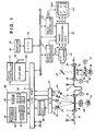
- Fig.1 schematically shows the color film analyzer of this invention. An
elongated film 10 is made of a plurality of color photographic films such as color negative films bonded together with a splice tape. Each of the color negative films has a plurality of color negative picture frames. A notch is formed for each picture frame near at the central line thereof. Theelongated film 10 is nipped with two sets offeed rollers notch sensor 13 detects the notch to supply the detected signal toCPU 15 via an I/O port 14. With a given distance between thenotch sensor 13 and a measuring station, it is possible to transform a particular picture frame correctly to the measuring station by moving theelongated film 10 for a predetermined time after detecting the notch. The predetermined time may be obtained by counting drive pulses of apulse motor 16 which drives thefeed roller pairs - A
film mask 18 is mounted at the measuring station. A picture frame positioned at the film mask is applied with light radiated from alamp 19 and converged by twoondenser lenses 20. The picture frame with light applied is measured with ascanner 21,sensors scanner 21 is constructed of alens 25 andimage area sensor 26 for photoelectric conversion of an image focussed onto the photosensitive region to output therefrom a time-sequential signal. The time sequential signal is converted into a digital signal by an A/D converter 27 to supply it to anoperation unit 28 constructed of an 8 bit microcomputer. Theoperation unit 28 logarithm-converts the measured light data of pixels to obtain density values which are written in a memory. After this write operation, the density values for pixels within a predetermined area are read to obtain an arithmetic mean value thereof. A plurality of mean density values for predetermined areas such as the central area of a picture frame, upper and lower areas and the like, are obtained. The distribution of the plurality of mean density values is used to identify a pattern classification. An operation formula prepared for each pattern classification is used to calculate a density correction value (color correction value common to three colors) which is stored inRAM 29. - The red, green and
blue sensors sensors 22 to 34 are converted into digital signals by the A/D converter to be supplied toCPU 15 via the I/O port 14 for calculation of color correction values and ND filter values for the three colors which are written inRAM 29. - A picture frame at the measuring station is then transported to an image pickup station, a buffer loop of the film being interposed therebetween. A
notch sensor 32 is mounted upstream of the image pickup station to transport a picture frame correctly to the image pickup station. Afilm mask 33 is mounted at the image pickup station. A picture frame positioned within thefilm mask 33 is applied with light radiated from alamp 35 and diffused by amixing box 34. Between themixing box 34 and thelamp 35, there are disposed twoND filters 36 which are driven by apulse motor 37 in opposite directions in a plane perpendicular to the optical path. In the ordinary case, theND filters 36 are inserted within the optical path at the normal position. They are retracted from the optical path for a picture frame of over-exposure, and further inserted within the optical path for a picture frame of under-exposure. - Two sets of
feed rollers pulse motor 40 are mounted on opposite sides of thefilm mask 33. The rotation of thepulse motor 40 is controlled by amotor controller 41 for sequentially positioning picture frames with notches at the image pickup station. Light passed through a positioned picture frame is reflected by amirror 43 and taken with aTV camera 44 which generates red, green and blue color image signals R, G and B, synchro signal SYNC, and field signal F. The red, green and blue color image signals R, G and B are processed by animage processing unit 45 and supplied to acolor monitor 46. Thecolor monitor 46, for example, a color CRT, displays a plurality of color images in a matrix arrangement on itsscreen 46a. Specifically, as shown in Fig.6, themonitor 46 displays four picture frames on each of four lines A to D in the vertical direction. The color images on line A are first inputted to the color monitor, and line D last inputted. A color image at a left hand on a line is first inputted. - A
write controller 47 under control ofCPU 15 generates an address signal and the like based on the synchro signal SYNC and field signal F to thereby control the write operation of image data to theimage processing unit 45. Aread controller 48 under control ofCPU 15 generates an address signal for reading image data, a synchro signal to be supplied to thecolor monitor 46, and the like. - A
keyboard 50 hascolor keys 51,density keys 52,operation keys 53,alphanumeric keys 54, pictureframe designating key 55, next page key 56, andsize designating keys 57. Thecolor keys 51 include cyan keys for cyan correction, magenta keys for magenta correction, and yellow keys for yellow correction, respective keys for the same color being constructed of a plurality of keys for stepwise color correction. Thedensity keys 52 for density correction are constructed of a plurality of keys arranged laterally for stepwise density correction. Theoperation keys 53 are used for indicating film inspection start, printing of correction data, and the like. Thealphanumeric keys 54 are used for setting print conditions, inputting data and the like. The pictureframe designating keys 55 for designating a picture frame to be corrected manually are constructed of 16 keys in one-to-one correspondence with 16 picture frames. The next page key 56 is used to move the display on the color monitor 46 to the next page. Thesize designating keys 57 are used for inputting the picture frame size of a color photographic film. It is to be noted that since a DX code representative of the type of a color photographic film is printed on the side thereof, a DX sensor may be mounted on the passage of theelongated film 10 to automatically input the picture frame size. Discrimination between "135 F" and "135 H" may be conducted based on the interval between picture frames. - A
puncher 60 is used after film inspection to record exposure correction data (color, density correction values) in apunch tape 61.ROM 62 stores therein fixed data such as print conditions, and programs for control of circuit operation. - Fig.2 shows the detail of the
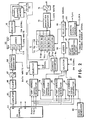
image processing unit 45, wherein only the red color image signal processing unit is shown because the other green and blue color image signal processing units have the same construction as that of the red color image signal processing unit. A red color image signal supplied from theTV camera 44 is amplified by anamplifier 65 and sent to aclamp circuit 66 to establish a reference level. The red color image signal outputted from theclamp circuit 66 is converted into a digital signal by an A/D converter 67 and sent to alogarithmic converter 68 constructed of look-up table memories which logarithm-convert an inputted signal to obtain image data proportional to the density value.CPU 15 writes table data stored inROM 62 to thelogarithmic converter 68 prior to image pickup by theTV camera 44. - A
chroma correction circuit 69 is used for correcting a difference between spectral sensitivities of the color paper used by a color printer and the image pickup area of theTV camera 44. Thechroma correction circuit 69 is constructed of three look-up table memories 69a for weighting three color image data and anadder 69b for adding together the outputs from the three look-up table memories 69a and outputting the result as red color image data. Prior to start film inspection,CPU 15 read three sets of coefficients stored inROM 62 to change stepwise the read-out coefficients and generate three types of table data for red color chroma correction, the table data being written in an associated one of the three look-up table memories 69a. - A
selector 70 operates in response to a switching signal SW fromCPU 15 to send image data for "135 F" and "110 type"film 10 to theimage memory 71, and for "135 H" via abuffer memory 72 to theimage memory 71. Thebuffer memory 72 is used to rotate an image of a picture frame by 90 degrees. One picture frame is composed of 256 x 256 pixels (64 K pixels in total), and the gradation of each pixel of each of the three primary colors is represented by 8 bits. Therefore, thebuffer memory 72 is constructed of eight RAMs 721 to 728 each having a memory capacity of 64 K x 1 bits. - An
image memory 71 is constructed of a plurality of memory boards corresponding in number to that of gradation levels, each memory card being constructed of four RAMs corresponding to four lines A to D on which color images are displayed in a matrix arrangement. In this embodiment, eightmemory boards 711 to 718 are used, each memory board being constructed of four RAMs (256 K x 1 bits).RAM 711a has four memory areas A1 to A4 in each of which image data of a single picture frame are stored. Theother RAMs 711b to 711d are similarly constructed, with memory areas given like reference characters and figures to those shown in Fig.6. Each RAM may be constructed of four RAMs of 64 K x 1 bits instead of 256 K x 1 bits. An image memory having a capacity of two or more pages may be used for allowing both read and write operations simultaneously, without intercepting film inspection while writing image data. - Image data read out from the
image memory 71 are sent to agradation converter circuit 73 whereat the image data are subjected to negative-to-positive conversion and gradation conversion. Thegradation converter circuit 73 is constructed of sixteen look-up table memories corresponding to sixteen picture frames. Table data stored in each look-up table memory are used for image processing. Table data are generated by changing reference table data in accordance with the light measured results or by manually inputting correction values. The image data of a picture frame undergone the gradation conversion are sent to a D/A converter 74 and converted into a red color analog signal which is then sent to thecolor monitor 46. - For the purpose of writing image data in the
buffer memory 72 and theimage memory 71, four addresssignal generating circuits 78 to 81 are provided. The addresssignal generating circuits TV camera 44, using the synchro signals (H sync and V sync), field signal outputted from the TV camera and clock signals from aclock generator 82. In order to temporarily store image data for "135 H" in thebuffer memory 72, an address signal from theaddress signal generator 78 is sent to thebuffer memory 72 via aselector 83. In transferring image data from thebuffer memory 72 to theimage memory 71, an address signal from the addresssignal generating circuit 79 is sent to anaddress converter circuit 84 which interchanges the horizontal address with the vertical address to rotate the picture frame by 90 degrees. Theselector 83 selects address signals in accordance with the switching signal SW from thewrite controller 47. - A
selector 85 under control of thewrite controller 47 selects one of three address signals outputted from the addresssignal generating circuits 79 to 81. The selected address signal is sent to anadder 86 and added to a start address outputted from a startaddress designating circuit 87, the addition result being sent to theimage memory 71 via aselector 88. The startaddress designating circuit 87 is used for designating a memory area among the sixteen memory areas in which image data are to be written. Theselector 88 selects either one of a write address signal outputted from theadder 86 and a read address signal outputted from an addresssignal generating circuit 89. - Next, the operation of film inspection will be described. First, the
elongated film 10 already developed is set at the analyzer. Then, in order to make the inspection conditions of the color film analyzer match the exposure conditions of the color printer, thealphanumeric keys 54 on thekeyboard 50 are operated to designate a print channel corresponding to the color printer now in use. Next, thesize designating key 57 is operated to designate the film size, e.g., "135 F". - Upon instruction of the start of film inspection, the
elongated film 10 is transported in the direction indicated by the arrow. During transportation, a notch is detected with thenotch sensor 13. The amount of film transportation is controlled based on the time when the notch is detected, to thereby position the picture frame with the first notch at the measuring station. The picture frame at the measuring station is then applied with light from thelamp 19. Each point on the negative image within the picture frame is sequentially measured with thescanner 21. The LATD values for red, green and blue are measured by theLATD sensors 22 to 24. After the measurement, thepulse motor 16 is again driven to transport the picture frame with the second notch to the measuring station to conduct such measurement. The picture frames with the third notch and following notches are similarly measured at the measuring station. - The first picture frame after subjected to the measurement is further transported to the image pickup station during which the
notch sensor 32 detects the notch of the first picture frame. The amount of film transportation is controlled based on the time when the notch is detected, to thus position the first picture frame correctly at the image pickup station. Until such time when the first picture frame is set at the image pickup station, it has been judged if the picture frame is over-exposure or under-exposure based on the measurement results by theLATD sensors 22 to 24. For an over-exposed picture frame, the ND filters 36 are retracted from the optical path by driving thepulse motor 37 under control ofCPU 15 to thus apply strong light from thelamp 35 to the picture frame. On the other hand, for an under-exposed picture frame, the ND filters 36 are further inserted into the optical path to reduce the light intensity. - Since the position of the ND filters 36 have been adjusted until such time when the first picture frame is positioned at the image pickup station, the image of the first picture frame is ready for being taken with the TV camera immediately after the first picture frame reaches the image pickup station. Time-sequential red, green and blue image signals outputted from the
TV camera 44 are sent to theimage processing unit 45 whereat the signals undergo A/D conversion, chroma correction, storage and gradation conversion. Specifically, as shown in Fig.2, a red image signal is subjected to amplification and reference level clamping and thereafter, the signal is converted into red digital image data by the A/D converter. The red image data are made proportional to the density value by thelogarithmic converter 68 and sent to thechroma correction circuit 69. The chroma corrected red image data are then stored in theimage memory 71 via theselector 70. - In synchro with processing the red image, the
address generating circuits 78 to 81 start operating. Since the color negative film now used by way of example is "135 F", an address signal from the addresssignal generating circuit 79 is selected by theselector 85 and sent to theadder 86. During the image pickup of the first picture frame, the startaddress designating circuit 87 outputs an address representative of the origins of the first memory areas A1 of thememory boards 711 to 718. The address signal from theselector 85 and the origin address signal are added and sent to theimage memory 71 via theselector 88. Image data for one pixel for each color has 8 bits. Therefore, 8 bit red image data are sequentially written in the eightmemory boards 711 to 718 at the designated addresses. The following red image data are written into theimage memory 70 via theselector 70. Green and blue image data are also written into theimage memory 71 in the similar manner. - Upon completion of writing the image data of the first picture frame, the
pulse motor 40 again starts rotating to position the second picture frame at the image pickup station. Thewrite controller 47 sends an image picked-up frames number signal to the startaddress designating circuit 87 which outputs the origin address signal representative of the second memory areas A2 of thememory boards 711 to 718. - Image data for 16 picture frames are thus sequentially taken with the
TV camera 44 and written into theimage memory 71. After this, theread controller 48 sets theimage memory 71 in a read mode. An address signal outputted from theaddress generating circuit 89 is selected by theselector 88 and sent to theimage memory 71. The image data written in theimage memory 71 at the address are read and sent to thegradation converter circuit 73 which selects the look-up table corresponding to the picture frame now concerned and converts the image data in accordance with the table data stored therein. The table data stored in each look-up table differ for each picture frame, and are generated by shifting reference table data in accordance with the density correction value measured with thescanner 21 and the color correction values measured with theLATD sensors 22 to 24. - The image data after subjected to gradation conversion are converted into an analog signal by the D/
A converter 73. The obtained red image analog signal is sent to thecolor monitor 46. The green and blue image data are similarly read so that 16color images 92 are displayed on the color monitor 45 as shown in Fig.6. In reality, 16color images 92 are separated from adjacent images with a white marginal frame interposed therebetween. An operator observes 16frame color images 92 to judge if the images can be printed properly or not. For a color image which is considered not proper, the pictureframe designating key 55 of thekeyboard 50 is operated to designate such a picture frame. Upon this designation, aframe designating cursor 93 is displayed on the designated color image at a suitable position thereof. Next, thecolor key 51 ordensity key 52 is operated to input a correction value. Upon input of the correction value, the table data of the look-up table for gradation conversion of the designated picture frame are renewed. The image data are converted in accordance with the renewed table data so that the color image of the designated picture frame is corrected and displayed. If such correction is still insufficient, thecolor key 51 ordensity key 52 is again operated to further correct the color image. - If it is judged that all the picture frames will result in proper prints, then the next page key 56 is operated to conduct image pickup with the TV camera, simulation of printed images, and display of color images, to thus perform film inspection for 16 picture frames.
- Upon completion of film inspection for all picture frames on the
elongated film 10, theoperation key 53 is operated so that the exposure correction data for respective picture frames stored inRAM 29 are recorded in thepunch tape 61 using thepuncher 88. The correction data includes correction data automatically calculated using thescanner 21 and correction data manually inputted by the operator. In printing frame pictures, thepunch tape 61 is set at the printer to read therefrom the correction data which are added to the LATD value for each color measured with LATD sensor built in the printer, to thus determine the exposure amount for each color. - In the case where film inspection for "135 H" is performed, the
size designating key 57 is first operated to input the film size. In this case, the image data read from a picture frame of "135 H" are written in thebuffer memory 72 at the area designated by the address signal from the addresssignal generating circuit 78. After writing the image data into thebuffer memory 72, the address signal from the addresssignal generating circuit 79 is sent to theaddress converter circuit 84 whereat the vertical address and horizontal address are interchanged. Using the interchanged addresses, the image data are read from the buffer memory and written in theimage memory 71 at the area designated by the address signal from theaddress designating circuit 79. - As above, in the case of "135 H", the image data of each picture frame are written from the
buffer memory 72 into theimage memory 71. After completion of writing image data for 16 picture frames, the image data are read from theimage memory 71 and sent to the color monitor 46 which displays 16 color images in a matrix arrangement at the same dimension as that of "135 F". However, the vertical and horizontal addresses are interchanged for "135 H" so that the color images are rotated by 90 degrees and turned sideways. - In the case where inspection for "110 type" color negative film is performed, the address
signal generating circuit 81 is activated to designate the address of theimage memory 71 in accordance with an address signal outputted from the addresssignal generating circuit 81. The image data read with the TV camera are then written into theimage memory 71. Color images for "110 type" color negative film are displayed on the color monitor 46 at the same dimension and posture as those for "135 F" as shown in Fig.6. - The
elongated film 10 may sometimes include, although less in amount, "135 H" and "110 type" color negative films. Fig.7 partially shows an example of theelongated film 10 which has both a "135 F" color negative film and a 135 H" color negative film bonded to the former using a splice tape. For clearly showing the joint portion between two color negative films, the splice tape portion is displayed as asplice frame 94 on the color monitor. In Fig.7, thecolor images 95a and 95b for the first two picture frames are displayed turned sideways, whereas the color image 96n for the last picture frame of "135 F" is displayed at the right of thesplice frame 94. - Next, the relationship between the effective image pickup area of a TV camera and the image memory will be described with reference to Figs.3 to 5. The effective image pickup area 100 (hereinafter simply called image pickup area) of the
TV camera 44 has 512 scan lines in the vertical direction. The even number represent scan lines for 0 field, and the odd number represents scan lines for 1 field (interlaced field). Sampling image data is performed 512 times for each scan line. Therefore, image data for a picture frame have 512 pixels both in the vertical and horizontal directions. Image data for a picture frame is accordingly constructed of 256 K pixels. - The
image memory 71 is composed of the image areas each constructed of 64 K bits for storage of 64 K pixels. For "135 H", image data thinned in both the vertical and horizontal directions every second pixel among 256 K pixels included in the image pickup area are written in theimage memory 71. Specifically, the image data of 0 field only as thinned every second pixel in the horizontal direction are used. This pixel thinning is performed using the addresssignal generating circuit 80. Therefore, image data of 64 K pixels thinned in both the vertical and horizontal directions are stored in theimage memory 71 as shown in Fig.4A wherein "X" represents the address in the horizontal direction, and "Y" represents the address in the vertical direction, and the "H" and "Y" in the parenthesis represent the directions on theimage pickup area 100 shown in Fig.3. - Since the optical magnification factor is fixed such that the
image pickup area 100 of theTV camera 44 coincides with the picture frame of "135 F", the size of a picture frame of "135 H" becomes an area indicated by hatching lines of Fig.3. This hatching area starts from the N-th pixel to (N + 255)-th pixel in the horizontal direction. The addresssignal generating circuit 78 functions to read all the pixels including N-th to (N + 255)-th pixel without thinning for both 0 and 1 fields, and write them in thebuffer memory 72. Since an image for "135 H" is a vertically elongated shape, the pixels are thinned in the vertical direction by 1/2. Thus, 256 pixels in both the vertical and horizontal directions, 64 K pixels in total, are read and written in thebuffer memory 72. - The image data written in the
buffer memory 72 are read in accordance with the interchanged vertical and horizontal addresses, and written in theimage memory 71. The image data of 64 K pixels are written in theimage memory 71 while being rotated by 90 degrees as shown in Fig.4B. It is noted that the ratio of vertical and horizontal lengths of thecolor monitor 46 is 3:4 so that the image is displayed in a compressed state in the vertical direction. In view of this, it is preferable to thin pixels every fifth pixel in the horizontal direction in writing the image data in thebuffer memory 72. - The size of a picture frame for a "110 type" color negative film becomes as indicated by cross-hatching lines shown in Fig.3. This cross-hatching area starts from N-th to (N + 255)-th pixels in the horizontal direction and from M-th to (M + 255)-th pixels in the vertical direction. Since both the vertical and horizontal directions have each 256 pixels, the image data are written in the
image memory 71 without performing pixel thinning. - As described above, pixels for "135 F" are thinned in both the directions by "1/2" to make the total number of pixels equal to that for "110 type". Pixels for "135 H" are thinned in the vertical direction only to make the total pixel number equal to that for "110 type". Accordingly, color images of picture frames for "135 F", "135 H" and "110 type" are all displayed at the same dimension on the
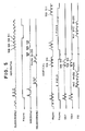
color monitor 46. - Fig.5 shows timing charts used for explaining the write operation of pixels. As seen from Fig.5, there are shown the timings for writing pixels for "135 F" and "110 type" into the
image memory 71 and pixels for "135 H" into thebuffer memory 72. - In the above embodiment, a plurality of color images for picture frames are displayed in a matrix arrangement on the color monitor. However, the present invention is also applicable to the case where a color image for a single picture frame is displayed on the color monitor at a magnified dimension. Further, reference images giving proper prints may be displayed at D line for convenience of film inspection. Furthermore, instead of a color CRT, a liquid crystal display and the like may be used as the color monitor.
- While a preferred embodiment of the invention has been described using specific terms, such description is for illustrative purposes only, and it is to be understood that changes and variations may be made without departing from the spirit or scope of the following claims.
Claims (15)
picking up the image data for a large-size picture frame by thinning the pixels within an image pickup area of said image pickup means one pixel out of a predetermined number of pixels, and picking up the image data for a small-size picture frame by picking up all the pixels within a specific area of said image pickup area determined in accordance with the size of said picture frame;
writing said picked-up image data into an image memory; and
reading said image data from said image memory and supplying said read-out image data to said image display means for display of the image of said picture frame.
means for picking up the image data for a large-size picture frame by thinning the pixels within an image pickup area of said image pickup means one pixel out of a predetermined number of pixels, and picking up the image data for a small-size picture frame by picking up all the pixels within a specific area of said image pickup area determined in accordance with the size of said picture frame; and
writing said picked-up image data into an image memory.
Applications Claiming Priority (4)
| Application Number | Priority Date | Filing Date | Title |
|---|---|---|---|
| JP25115/88 | 1988-02-05 | ||
| JP25114/88 | 1988-02-05 | ||
| JP63025115A JPH082096B2 (en) | 1988-02-05 | 1988-02-05 | Image data import method |
| JP63025114A JPH01200879A (en) | 1988-02-05 | 1988-02-05 | Picture data fetch method |
Publications (3)
| Publication Number | Publication Date |
|---|---|
| EP0327112A2 true EP0327112A2 (en) | 1989-08-09 |
| EP0327112A3 EP0327112A3 (en) | 1989-08-30 |
| EP0327112B1 EP0327112B1 (en) | 1994-06-15 |
Family
ID=26362709
Family Applications (1)
| Application Number | Title | Priority Date | Filing Date |
|---|---|---|---|
| EP89101935A Expired - Lifetime EP0327112B1 (en) | 1988-02-05 | 1989-02-03 | Method and apparatus for displaying picture frames of color photograhic films |
Country Status (3)
| Country | Link |
|---|---|
| US (1) | US4991004A (en) |
| EP (1) | EP0327112B1 (en) |
| DE (1) | DE68916049T2 (en) |
Cited By (2)
| Publication number | Priority date | Publication date | Assignee | Title |
|---|---|---|---|---|
| EP0361739A2 (en) * | 1988-09-29 | 1990-04-04 | Sony Corporation | Scanning apparatus for reading an image |
| WO1992005470A1 (en) * | 1990-09-17 | 1992-04-02 | Eastman Kodak Company | User-interactive reduction of scene balance failures |
Families Citing this family (21)
| Publication number | Priority date | Publication date | Assignee | Title |
|---|---|---|---|---|
| JP2921879B2 (en) * | 1989-09-29 | 1999-07-19 | 株式会社東芝 | Image data processing device |
| US5161035A (en) * | 1989-10-31 | 1992-11-03 | Brother Kogyo Kabushiki Kaisha | Digital image processing device for enlarging original image with high fidelity |
| US6191810B1 (en) * | 1990-09-13 | 2001-02-20 | Fuji Photo Film Co., Ltd. | Film image input system for outputting an image signal to a video monitor |
| US6166762A (en) | 1990-09-13 | 2000-12-26 | Fuji Photo Film Co., Ltd. | Film image input system |
| US5440401A (en) * | 1990-09-14 | 1995-08-08 | Eastman Kodak Company | Image database incorporating low resolution index image data |
| US5138459A (en) * | 1990-11-20 | 1992-08-11 | Personal Computer Cameras, Inc. | Electronic still video camera with direct personal computer (pc) compatible digital format output |
| JPH05130544A (en) * | 1991-10-31 | 1993-05-25 | Sony Corp | Video signal processing device |
| US5184227A (en) * | 1991-11-21 | 1993-02-02 | Eastman Kodak Company | Photographic printer with index print generation |
| DE69231942T2 (en) * | 1991-11-22 | 2002-04-04 | Eastman Kodak Co | Method and device for controlling the rapid display of multiple images from a digital image database |
| US6646679B2 (en) * | 1991-11-22 | 2003-11-11 | Minolta Co., Ltd. | Still image reproducing apparatus saving time for still image reproduction |
| JP2597802B2 (en) * | 1992-08-04 | 1997-04-09 | インターナショナル・ビジネス・マシーンズ・コーポレイション | Method for controlling an image capture device, image capture device and user interface |
| JP2914471B2 (en) * | 1993-06-15 | 1999-06-28 | ノーリツ鋼機株式会社 | Monitor image calibration system for image printer |
| US5685002A (en) * | 1993-09-29 | 1997-11-04 | Minolta Co., Ltd. | Image processing system capable of generating a multi-picture image |
| JP3367062B2 (en) * | 1994-01-10 | 2003-01-14 | 富士写真フイルム株式会社 | Print ordering equipment |
| JP3377278B2 (en) * | 1994-02-21 | 2003-02-17 | 富士写真フイルム株式会社 | Index print making device |
| EP0698993B1 (en) | 1994-08-22 | 2002-01-23 | Nikon Corporation | Image reading device and method |
| US5546196A (en) * | 1995-02-17 | 1996-08-13 | Eastman Kodak Company | Supplemental photofinishing data system |
| JPH09181903A (en) * | 1995-12-22 | 1997-07-11 | Fuji Photo Film Co Ltd | Image reproduction method and device therefor |
| JP2001169160A (en) * | 1999-12-14 | 2001-06-22 | Minolta Co Ltd | Digital camera and image display method for digital camera |
| JP3991543B2 (en) | 2000-01-11 | 2007-10-17 | 株式会社日立製作所 | Imaging device |
| JP2006174334A (en) * | 2004-12-20 | 2006-06-29 | Seiko Epson Corp | Display controller, electronic apparatus and image data supply method |
Citations (5)
| Publication number | Priority date | Publication date | Assignee | Title |
|---|---|---|---|---|
| US4279505A (en) * | 1978-10-20 | 1981-07-21 | Gretag Aktiengesellschaft | Method for print exposure control |
| EP0085351A2 (en) * | 1982-01-29 | 1983-08-10 | Kabushiki Kaisha Toshiba | Picture information display device |
| EP0108158A1 (en) * | 1982-11-04 | 1984-05-16 | Konica Corporation | Image display system |
| GB2177567A (en) * | 1985-06-27 | 1987-01-21 | Ibm | Image conversion apparatus |
| US4692797A (en) * | 1984-12-07 | 1987-09-08 | Fuji Photo Film Co., Ltd. | Photographic printing system |
Family Cites Families (6)
| Publication number | Priority date | Publication date | Assignee | Title |
|---|---|---|---|---|
| JPS60218974A (en) * | 1984-04-16 | 1985-11-01 | Canon Inc | Facsimile equipment |
| JPS61252762A (en) * | 1985-04-30 | 1986-11-10 | Toshiba Corp | Image forming device |
| JPS6229239A (en) * | 1985-07-30 | 1987-02-07 | Toshiba Corp | Frame synchronizing system in cyclic information transmitter |
| JPS62141530A (en) * | 1985-12-16 | 1987-06-25 | Fuji Photo Film Co Ltd | Color negative testing device |
| JPS62154853A (en) * | 1985-12-26 | 1987-07-09 | Canon Inc | Image reader |
| US4807156A (en) * | 1987-03-23 | 1989-02-21 | Xerox Corporation | Adjustable print size control for raster output scanners |
-
1989
- 1989-02-03 DE DE68916049T patent/DE68916049T2/en not_active Expired - Lifetime
- 1989-02-03 EP EP89101935A patent/EP0327112B1/en not_active Expired - Lifetime
- 1989-02-03 US US07/305,599 patent/US4991004A/en not_active Expired - Lifetime
Patent Citations (5)
| Publication number | Priority date | Publication date | Assignee | Title |
|---|---|---|---|---|
| US4279505A (en) * | 1978-10-20 | 1981-07-21 | Gretag Aktiengesellschaft | Method for print exposure control |
| EP0085351A2 (en) * | 1982-01-29 | 1983-08-10 | Kabushiki Kaisha Toshiba | Picture information display device |
| EP0108158A1 (en) * | 1982-11-04 | 1984-05-16 | Konica Corporation | Image display system |
| US4692797A (en) * | 1984-12-07 | 1987-09-08 | Fuji Photo Film Co., Ltd. | Photographic printing system |
| GB2177567A (en) * | 1985-06-27 | 1987-01-21 | Ibm | Image conversion apparatus |
Cited By (4)
| Publication number | Priority date | Publication date | Assignee | Title |
|---|---|---|---|---|
| EP0361739A2 (en) * | 1988-09-29 | 1990-04-04 | Sony Corporation | Scanning apparatus for reading an image |
| EP0361739A3 (en) * | 1988-09-29 | 1991-01-09 | Sony Corporation | Scanning apparatus for reading an image |
| US5133025A (en) * | 1988-09-29 | 1992-07-21 | Sony Corporation | Scanning apparatus for reading an image |
| WO1992005470A1 (en) * | 1990-09-17 | 1992-04-02 | Eastman Kodak Company | User-interactive reduction of scene balance failures |
Also Published As
| Publication number | Publication date |
|---|---|
| US4991004A (en) | 1991-02-05 |
| DE68916049T2 (en) | 1994-09-22 |
| EP0327112A3 (en) | 1989-08-30 |
| EP0327112B1 (en) | 1994-06-15 |
| DE68916049D1 (en) | 1994-07-21 |
Similar Documents
| Publication | Publication Date | Title |
|---|---|---|
| EP0327112B1 (en) | Method and apparatus for displaying picture frames of color photograhic films | |
| US4364084A (en) | Color correction monitoring system | |
| US4935809A (en) | Color film analyzing method and apparatus | |
| US5184227A (en) | Photographic printer with index print generation | |
| US4782390A (en) | Color negative inspection apparatus for displaying and sequentially shifting N color positive images corresponding to N color negative frames | |
| CN100399789C (en) | Image forming device | |
| US5018023A (en) | Image input method | |
| JPS63305335A (en) | Method and device for correcting shading of video printer | |
| JP2518883B2 (en) | How to display frame specified cursor | |
| JPH01179139A (en) | Video system color film analizer | |
| JPH0196634A (en) | Index photograph printing method | |
| JPH082096B2 (en) | Image data import method | |
| JP2501854B2 (en) | Video type color film analyzer | |
| JPH03153228A (en) | Trimming photographic printer | |
| JP3605812B2 (en) | Exposure control method for film scanner | |
| JP2501853B2 (en) | Video type color film analyzer | |
| JPH01200879A (en) | Picture data fetch method | |
| JPH01200349A (en) | Video color film analyzer | |
| JP2637260B2 (en) | Trimming correction system | |
| JPS61138945A (en) | Inspection device for color film | |
| JPH01198735A (en) | Video type color film analyzer | |
| JPH01224745A (en) | Video type color film analyzer | |
| JPH06326840A (en) | Picture printing system | |
| JPH06236004A (en) | Deteriorated image recoverying system | |
| JPH0279173A (en) | Picture inputting method |
Legal Events
| Date | Code | Title | Description |
|---|---|---|---|
| PUAI | Public reference made under article 153(3) epc to a published international application that has entered the european phase |
Free format text: ORIGINAL CODE: 0009012 |
|
| PUAL | Search report despatched |
Free format text: ORIGINAL CODE: 0009013 |
|
| AK | Designated contracting states |
Kind code of ref document: A2 Designated state(s): DE FR GB |
|
| RHK1 | Main classification (correction) |
Ipc: H04N 1/393 |
|
| AK | Designated contracting states |
Kind code of ref document: A3 Designated state(s): DE FR GB |
|
| 17P | Request for examination filed |
Effective date: 19891114 |
|
| 17Q | First examination report despatched |
Effective date: 19920730 |
|
| GRAA | (expected) grant |
Free format text: ORIGINAL CODE: 0009210 |
|
| AK | Designated contracting states |
Kind code of ref document: B1 Designated state(s): DE FR GB |
|
| REF | Corresponds to: |
Ref document number: 68916049 Country of ref document: DE Date of ref document: 19940721 |
|
| ET | Fr: translation filed | ||
| PLBE | No opposition filed within time limit |
Free format text: ORIGINAL CODE: 0009261 |
|
| STAA | Information on the status of an ep patent application or granted ep patent |
Free format text: STATUS: NO OPPOSITION FILED WITHIN TIME LIMIT |
|
| 26N | No opposition filed | ||
| REG | Reference to a national code |
Ref country code: GB Ref legal event code: IF02 |
|
| REG | Reference to a national code |
Ref country code: GB Ref legal event code: 732E |
|
| REG | Reference to a national code |
Ref country code: FR Ref legal event code: CD Ref country code: FR Ref legal event code: TP |
|
| PGFP | Annual fee paid to national office [announced via postgrant information from national office to epo] |
Ref country code: GB Payment date: 20080130 Year of fee payment: 20 Ref country code: DE Payment date: 20080131 Year of fee payment: 20 |
|
| PGFP | Annual fee paid to national office [announced via postgrant information from national office to epo] |
Ref country code: FR Payment date: 20080208 Year of fee payment: 20 |
|
| REG | Reference to a national code |
Ref country code: GB Ref legal event code: PE20 Expiry date: 20090202 |
|
| PG25 | Lapsed in a contracting state [announced via postgrant information from national office to epo] |
Ref country code: GB Free format text: LAPSE BECAUSE OF EXPIRATION OF PROTECTION Effective date: 20090202 |