EP0327340A2 - Decoder circuit - Google Patents
Decoder circuit Download PDFInfo
- Publication number
- EP0327340A2 EP0327340A2 EP89300971A EP89300971A EP0327340A2 EP 0327340 A2 EP0327340 A2 EP 0327340A2 EP 89300971 A EP89300971 A EP 89300971A EP 89300971 A EP89300971 A EP 89300971A EP 0327340 A2 EP0327340 A2 EP 0327340A2
- Authority
- EP
- European Patent Office
- Prior art keywords
- potential
- transistor
- decoder circuit
- signal
- transistors
- Prior art date
- Legal status (The legal status is an assumption and is not a legal conclusion. Google has not performed a legal analysis and makes no representation as to the accuracy of the status listed.)
- Granted
Links
Images


Classifications
-
- H—ELECTRICITY
- H03—ELECTRONIC CIRCUITRY
- H03M—CODING; DECODING; CODE CONVERSION IN GENERAL
- H03M7/00—Conversion of a code where information is represented by a given sequence or number of digits to a code where the same, similar or subset of information is represented by a different sequence or number of digits
-
- G—PHYSICS
- G11—INFORMATION STORAGE
- G11C—STATIC STORES
- G11C8/00—Arrangements for selecting an address in a digital store
- G11C8/10—Decoders
Definitions
- the present invention relates to a decoder circuit, more particularly, to an output portion or a buffer portion of a dynamic type decoder circuit used for selecting a memory cell of a memory device.
- a decoder circuit is used for decoding an input signal, and selecting and outputting a signal on one of a plurality of signal conductors.
- a decoder circuit is used for various purposes, but in the example given below, the decoder circuit is used for selecting a memory cell of a memory such as a ROM (Read Only Memory) or PLA (Programmable Logic Array), and the like.
- one type of decoder circuit comprises a decoder portion, a buffer portion, and a control portion.
- the decoder portion includes input signal conductors and output signal conductors, the input signal conductors being complemental signal conductors and the output signal conductors being provided so as to cross the input signal conductors.
- a cell transistor is provided for each crossed portion of the input signal conductors and the output signal conductors, and one of the output signal conductors is selected in accordance with a decoded logic of the contents of the input signals.
- Output portions of the output signal conductors are provided, for example, with NAND circuits, and the input terminal of each of the NAND circuits is connected to one of the output signal conductors and the other input terminal thereof is supplied with a timing signal.
- This timing signal is input to the other input terminals thereof after changing a potential of the output signal conductors, except one selected output signal conductor, to a low level. Namely, the timing signal is used to avoid a selection error, and this timing signal is output from a control portion in the decoder circuit.
- the control portion comprises, for example, an inverter having an input supplied with a potential of a dummy signal conductor wired in the same manner as the output signal conductors, a NAND circuit, and an inverter.
- the above type of decoder circuit has problems in that the timing signal should be applied to the NAND circuit, and the word lines should be driven by the timing signal through the NAND circuit in the output portions of the output signal conductors. Namely, the timing signal should be generated after all unselected output signal conductors have been fully discharged. Therefore, an output timing of the timing signal must include a time margin, taking into consideration a discharge time for fully discharging an electrical charge in each of the output signal conductors, whereby a drive timing of the word line corresponding to the selected output signal conductor is delayed and thus hinders a high speed operation of the decoder circuit. Further, the NAND circuits in the output portions of the output signal conductors and the control portions must be provided, and thus the construction of the decoder circuit becomes complicated.
- a decoder circuit including a plurality of signal conductors, a first potential setting means connected to said signal conductors and operable to set a potential of said signal conductors at a first potential, and a second potential setting means connected to said signal conductors and operable to maintain a potential of one of said signal conductors at said first potential and to reduce a potential of remaining said signal conductors to a second potential
- said decoder circuit comprises: a respective transfer transistor provided for each signal conductor, a gate electrode of each transfer transistor being connected to the corresponding signal conductor, a source electrode thereof being connected to another signal conductor, whereby in use, one of said transfer transistors is switched ON and a decoded output signal output when a gate potential of that transfer transistor is maintained at said first potential and a source potential thereof is brought to said second potential.
- An embodiment of the present invention may provide a decoder circuit having a simple configuration, a high speed operation and stable operation, and suitable for application to a large scale integration circuit.
- a decoder circuit is used for decoding input signals, and selecting and outputting one of a plurality of signal conductors.
- the decoder circuit is used for various purposes, but in the given below example, the decoder circuit is used for selecting a memory cell of a memory such as a ROM (Read Only Memory), and the like.
- Figure 1 is a block diagram showing one example of an existing decoder circuit applied to a read only memory.
- the decoder circuit 101 comprises a decoder portion 111, i.e., an AND-term portion, a buffer portion 112, and a control portion 113.
- the decoder circuit 101 is connected to a bit block 102, i.e., an OR-term portion, and selects one word line of the OR-term portion in accordance with an address signal of an input signal A0 - A2 , so that a bit data of an output signal is output from the bit block 102.
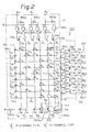
- FIG. 2 is a circuit diagram showing one example of the decoder circuit as shown in Fig. 1.
- This decoder circuit 101 is a dynamic type circuit wherein input signal conductors Y0 - Y2 are constructed by complemental signal conductors such as a pair of Y0 and Y0 , a pair of Y1 and Y1 , and a pair of Y2 and Y2 .
- Output signal conductors X0 - X7 are provided so as to cross the input signal conductors Y0 - Y2 .
- a cell transistor Cs is provided for each crossed portion of the input signal conductors Y0 - Y2 and the output signal conductors X0 - X7 , and one of the output signal conductors is selected in accordance with a decoded logic of the contents of the input signals A0 - A2.
- each cell transistor Cs is formed by an N-channel MIS transistor.
- input portions of the input signal conductors Y0 - Y2 are provided with NAND circuits NY0 - NY2′ to which input signals A0 - A2 , inverted signals A0 - A2 , of the input signals A0 - A2 , and a clock signal ⁇ are applied.
- one input terminal of the NAND circuits NY0 , NY1 , and NY2 is supplied with the input signals A0 , A1 , and A2 , respectively
- one input terminal of the NAND circuits NY0′, NY1′ and NY2′ is supplied with the inverted input signals A0 , A1 , and A2 inverted by inverter circuits INV0 , INV1 , and INV2 respectively
- the other input terminals of the all of the NAND circuits NY0 - NY2′ are supplied with the clock signal ⁇ .
- An output terminal of each of the NAND circuits NY0 - NY2′ is connected to the corresponding input signal conductors Y0 - Y2 through each of drive transistors D IN which are P-channel type MIS transistors, respectively.
- output portions of the output signal conductors X0 - X7 are provided with NAND circuits NX0- NX7 , and one input terminal of each of the NAND circuits NX0 - NX7 is connected to one of the output signal conductors X0 - X7.
- the other input terminal of each of the NAND circuits NX0 - NX7 is supplied with a timing signal Tc after changing a potential of the output signal conductors, except one selected output signal conductor, to a low level. Namely, the timing signal Tc is used to avoid a selection error, and this timing signal is output from a control circuit 113 in the decoder circuit 101.
- the control circuit 113 comprises an inverter INV3 having an input supplied with a potential of a dummy signal conductor DL wired in the same manner as the output signal conductance X0 - X7 , a NAND circuit N, and an inverter INV4.
- the other sides of the input signal conductors Y0 - Y2 are provided with discharge transistors T DC which are switched ON while the clock signal ⁇ is at a low level.
- These transistors are N-channel type MIS transistors, and gate electrodes thereof are supplied with an inverted clock signal ⁇ by an inverter IV5.
- the other sides of the output signal conductors X0 - X7 are provided with precharge transistors Tpc which are driven by the clock signal ⁇ .
- the precharge transistors Tpc which are P-channel type MIS transistors, are switched ON when the clock signal ⁇ is at a high level, and the output signal conductors X0 - X7 and the dummy signal conductor DL are precharged to a power source potential V DD .
- the output terminals of the NAND circuits NX0 - NX7 are connected to gate electrodes of the output transistors TR0 - TR7 (P-channel type MIS transistors), respectively.
- the drain electrodes of the output transistors TR0 - TR7 serve as output terminals O0 - O7 in this decoder circuit 101, and are connected, for example, to a cell array of the ROM 102 through word lines WD0 - WD7.
- the above described decoder circuit is formed by a C-MIS circuit, as shown in Fig. 2, wherein transistors shown by a thick line are P-channel type MIS (P-MIS) transistors and a transistor shown by a normal line is an N-channel type MIS (N-MIS) transistor, Note, an N-MIS transistor is switched ON when an input signal thereof is at a high level, and a P-MIS transistor is switched ON when an input signal thereof is at a low level.
- P-MIS P-channel type MIS
- N-MIS N-channel type MIS
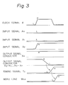
- a period during which the clock signal ⁇ is at a low level corresponds to a reset period of the decoder circuit 101, and a period during which the clock signal ⁇ is at a high level corresponds to an active period of the decoder circuit 101.
- the precharge transistors Tpc and the discharge transistors T DC are switched ON, all of the input signal conductors Y0 - Y2 are discharged, and all of the output signal conductors X0 - X7 are precharged.
- all output signals of the NAND circuits NY0 - NY2′ are at a high level, and thus all of the input transistors D IN are switched OFF.
- a potential of the selected output signal conductor X4 is maintained at the high level, and the other output signal conductors X0 - X3 and X5 - X7 are discharged and brought to a low level by each corresponding cell transistor Cs.
- the timing signal Tc (high level) is input to the NAND circuits NX0 - NX7 , after all of the unselected output signal conductors X0 - X3 and X5 - X7 are discharged, and thus an input of only the NAND circuit NX4 corresponding to the selected output signal conductor X4 is brought to a high level and a low level signal is output to an output transistor TR4. Consequently, only the output transistor TR4 is switched ON, and a word line WL4 is driven.
- the timing for generating the timing signal Tc is determined by a discharge time of the dummy signal conductor DL.
- the 'dummy signal conductor DL has the longest discharge time (or longer than the longest discharge time) among the output signal conductors X0 - X7.
- the dummy signal conductor DL is not selected (i.e., is always discharged) regardless of the address signals A0 - A2.
- a potential of the dummy signal conductor DL is always changed to a low level in a decoding operation, when an output signal conductor is selected.
- this signal of the dummy signal conductor DL is applied to an input of the inverter IV3 , and when the other input of a NAND circuit N is supplied with a high level enable signal EN from another circuit (not shown in the drawing) a high level timing signal Tc is output from an inverter IV4.
- the timing signal Tc must be output after it is confirmed that all of the unselected output signal conductors X0 - X3 and X5 - X7 are fully discharged, since an error may be generated such that a plurality of output signal conductors are selected when the timing signal Tc is applied before the discharge operation described above is completed.
- this type of decoder circuit 101 has problems in that the timing signal Tc should be applied to the NAND circuits and the word lines must be driven by the timing signal Tc through the NAND circuits NX0 - NX7. Namely, as understood from Fig. 3, the timing signal Tc must be generated after the all of the nonselected output signal conductors X0 - X3 and X5 - X7 are fully discharged.
- an output timing of the timing signal Tc must include a time margin, taking into consideration a discharge time for fully discharging an electrical charge in each of the output signal conductors X0 - X7 , and thus the drive timing of the word line WL4 corresponding to the selected output signal conductor X4 is delayed and hinders a high speed operation of the decoder circuit.
- the NAND circuits NX0 - NX7 of the buffer portion 112 and the control portion 113 including the inverter INV3 , the NAND circuit N, and the inverter INV4 must be provided and thus the construction of the decoder circuit becomes complicated. Furthermore, when C-MIS transistors are used, a NAND circuit is formed by four transistors, and thus a problem arises in a pattern layout of the decoder circuit, when the decoder circuit is used by a large scale integration circuit.
- the present invention may provide a decoder circuit having a simple configuration, a high speed and stable operation, and suitable for application to a large scale integration circuit.
- Figure 4 is a block diagram showing one embodiment of a decoder circuit according to the present invention.
- the decoder circuit 1 comprises a decoder portion 11, i.e., an AND-term portion, and a buffer portion 12. Namely, the control portion of the existing type decoder circuit is not needed for the present embodiment.
- the decoder circuit 1 is connected to a bit block 2, i.e., an OR-term portion, and selects one word line of the OR-term portion in accordance with an address signal of an input signal A0 - A2 , whereby bit data of an output signal is output from the bit block 2.
- FIG. 5 A circuit diagram of the embodiment according to the present invention is shown in Fig. 5.
- input signal conductors Y0 - Y2 are complemental signal conductors such as a pair of Y0 and Y0 , a pair of Y1 and Y1 , and a pair of Y2 and Y2 .
- Output signal conductors X0 - X7 are provided so as to cross the input signal conductors Y0 - Y2 .
- a cell transistor Cs is provided for each crossed portion of the input signal conductors Y0 - Y2 and the output signal conductors X0 - X7 , and one of the output signal conductors is selected in accordance with a decoded logic of the contents of the input signals A0 - A2.
- each cell transistor Cs is formed by an N-channel MIS transistor.
- input portions of the input signal conductors Y0 - Y2 are provided with NAND circuits NY0 - NY2′ to which input signals A0 - A2 , inverted signals A0 - A2 of the input signals A0 - A2 , and a clock signal ⁇ are applied.
- each input terminal of the NAND circuits NY0 , NY1 and NY2 is supplied with the input signals A0 , A1 , and A2
- each input terminal of the NAND circuits NY0′, NY1′ and NY2′ is supplied with the inverted input signals A0 , A1 and A2 inverted by inverter circuits INV0 , INV1 and INV2
- the other input terminals of all of the NAND circuits NY0 - NY2′ are supplied with the clock signal ⁇ .
- An output terminal of each of the NAND circuits NY0 - NY2′ is connected to the corresponding input signal conductors Y0 - Y2 through each of drive transistors D IN which are P-channel type MIS transistors, respectively.
- the decoder portion 11 of the decoder circuit 1 of the present embodiment has the same configuration as the existing circuit, but in the present embodiment, the configuration of the buffer portion 12 is simpler than that of the existing buffer portion, the present decoder circuit has a high speed and stable operation, and the present embodiment does not need the control portion necessary in the existing decoder circuit.
- an output end of each of the output signal conductors X0 - X7 is connected to a gate electrode of a corresponding transfer transistor T0 - T7 provided for each of the output signal conductors X0 - X7 , and a source electrode of each of the transfer transistors T0 - T7 is connected to a neighboring output signal conductor thereof.
- a gate electrode of the transfer transistor T0 is connected to a corresponding output signal conductor X0
- a source electrode thereof is connected to a neighboring output signal conductor X1.
- a gate electrode of the transfer transistor T1 is connected to a corresponding output signal conductor X1 , and a source electrode thereof is connected to a neighboring output signal conductor X2.
- a dummy signal conductor DL is discharged to a low level regardless of the address signals A0 - A2 , during a decoder operation, and thus the dummy signal conductor DL can be connected to a source electrode of a transfer transistor T7.
- a drain electrode of each of the transfer transistors T0 - T7 is connected to a gate electrode of each corresponding output transistor TR0 - TR7 and a drain electrode of each corresponding preset transistor PRT0 - PRT7 , respectively.
- a drain electrode of the transfer transistor T0 is connected to a gate electrode of a output transistor TR0 and a drain electrode of a preset transistor PRT0
- a drain electrode of the transfer transistor T1 is connected to a gate electrode of a output transistor TR1 and a drain electrode of a preset transistor PRT1.
- a source electrode of each preset transistor PRT0 - PRT7 and a source electrode of each output transistor TR0 - TR7 are supplied with a power supply potential V DD .
- each output transistor TR0 - TR7 is connected to each corresponding output terminal O0 - O7.
- a transfer transistor T0 - T7 a transfer transistor T0 - T7 , a preset transistor PRT0 - PRT7 and an output transistor TR0 - TR7 , are needed, and thus these three transistors can be provided in a small space between two adjacent signal conductors. Namely, a space between two adjacent signal conductors or each pitch of neighboring word lines is made smaller.
- the transfer transistors T0 - T7 are N-channel type MIS transistors
- the preset transistors PRT0 - PRT7 and the output transistors TR0 - TR7 are P-channel type MIS transistors.
- the output terminals O0 - O7 are connected to word lines WL0 - WL7 of the bit block 2.
- the bit block 2 is, for example, a read only memory having a plurality of word lines (WL1 - WL7), a plurality of bit lines and a plurality of memory cells.
- the other sides of the input signal conductors Y0 - Y2 are provided with discharge transistors T DC which are switched ON while the clock signal ⁇ is at a low level.
- These transistors are N-channel type MIS transistors, and the gate electrodes thereof are supplied with an inverted clock signal ⁇ by an inverter IV5.
- the other sides of the output signal conductors X0 - X7 are provided with precharge transistors Tpc driven by the clock signal ⁇ .
- the precharge transistors Tpc which are P-channel type MIS transistors, are switched ON when the clock signal ⁇ is at a low level, and the output signal conductors X0 - X7 and the dummy signal conductor DL are precharged at a high level.
- Figures 6 and 7 are circuit diagrams showing modifications of the embodiment of the decoder circuit shown in Fig. 5.
- the dummy signal conductor DL can be omitted.
- output signal conductors X0 - X7 are divided into pairs of two adjacent output signal conductors, a gate electrode of one transfer transistor of each pair is connected to one output signal conductor and a gate electrode of the other transfer transistor is connected to the other output signal conductor, and a source electrode of one transfer transistor is connected to the other output signal conductor and a source electrode of the other transfer transistor is connected to one output signal conductor, respectively.
- a gate electrode of a transfer transistor T0 is connected to the output signal conductors X0 and a source electrode of the transfer transistor T0 is connected to the output signal conductors X1
- a gate electrode of a transfer transistor T1 is connected to the output signal conductors X1 and a source electrode of the transfer transistor T1 is connected to the output signal conductors X0.
- a gate electrode of a transfer transistor T2 is connected to the output signal conductors X2 and a source electrode of the transfer transistor T2 is connected to the output signal conductors X3
- a gate electrode of a transfer transistor T3 is connected to the output signal conductors X3 and a source electrode of the transfer transistor T3 is connected to the output signal conductors X2.
- each of the output signal conductors X0 - X7 is connected to a gate electrode of each corresponding transfer transistor T0 - T7 , a source electrode of each transfer transistor T0 - T6 , except a last transfer transistor T7 , is connected to an adjacent output signal conductor X1 - X7 , except a first signal conductor X0.
- a source electrode of the last transfer transistor T7 is connected to the first output signal conductor X0.
- the dummy signal conductor DL can be omitted. Furthermore, a source electrode of each of the transfer transistors T0 - T7 is not only connected to an adjacent output signal conductor X1 - X7 and DL, which are connected to the gate electrode of the each of the transfer transistors T0 - T7 , but also the source electrode of each of the transfer transistors T0 - T7 can be connected to any one of the other signal conductors X0 - X7 and DL without connecting to a gate electrode thereof.
- a gate electrode of the transfer transistor T0 is connected to a corresponding output signal conductor X0 , and a source electrode thereof can be connected to another signal conductor X1, X2 , X3 , X4 , X5 , X6 , X7 or DL.
- a gate electrode of the transfer transistor T1 is connected to a corresponding output signal conductor X1 , and a source electrode thereof can be connected to another signal conductor X0 , X2 , X3 , X4 , X5 , X6 , X7 or DL.
- the above described decoder circuits are formed by a C-MIS circuit, and as shown in Figs. 5, 6, and 7, transistors drawn by a thick line are P-channel type MIS (P-MIS) transistors and a transistor shown by a normal line is an N-channel type MIS (N-MIS) transistor.
- P-MIS P-channel type MIS
- N-MIS N-channel type MIS
- only one transfer transistor (one of the select transistors T0 - T7) having a gate electrode connected to the selected output signal conductor, which is at a high level, is switched ON.
- the other transfer transistors having gate electrodes connected to the other non selected signal conductors are not switched ON, since both the gate electrodes and source electrodes thereof are at a low level.
- each node thereof is set to a specific potential in synchronization with a clock signal ⁇ , when the clock signal ⁇ is at a low level.
- a gate electrode of each of the present transistors PRT0 - PRT7 which are P-channel type MIS transistors, is at a low level, and then all of the preset transistors PRT0 - PRT7 are switched ON, whereby a gate potential of each of the output transistors TR0 -PR7 is precharged to a high level state.
- each input signal conductor Y0 - Y2 is discharged to a low level
- each output signal conductor X0 - X7 is precharged to a high level.
- a potential of the output signal conductor X4 is maintained at a high level, since all of the cell transistors connected to the output signal conductor X4 are kept OFF.
- the potential levels of the other non selected output signal conductors X0 - X3 and X5 - X7 are made low level.
- a potential level of the dummy signal conductor is also made low level.
- a gate potential of the transfer transistor T4 is kept at a high level, a source potential thereof is made low level, and the only one transfer transistor T4 is switched ON, since a voltage between the gate electrode and the source electrode is higher than a threshold voltage thereof.
- a transfer transistor T3 is kept OFF, since a source potential thereof is at a high level, a gate potential thereof is made low level, and a reverse bias is applied between the gate electrode and the source electrode thereof.
- the other transfer transistors T0 , T1, T2 , T5 , T6 and T7 are kept OFF, since both a gate potential and a source potential thereof are made low level. Note, in the other transfer transistors T0 , T1 , T2 , T5 , T6 and T7 , the gate potential thereof is made the same as the source potential thereof.
- the transfer transistor T4 when the transfer transistor T4 is switched ON and the other transfer transistors T0 - T3 and T5 - T7 are switched OFF, the relationship between a gate potential and a source potential of each of the other transfer transistors T0 - T3 and T5 - T7 is such that the gate potential is gradually made low level, and at the same time, the source potential is made low level.
- the gate potential and the source potential of each transfer transistor T0 , T1 , T2 , T5 , T6 and T7 are made equivalent to each other, and thus each transfer transistors T0 , T1 , T2 , T5 , T6 and T7 is made OFF, respectively. Consequently, the gate potential is not higher than the source potential, and thus an OFF state is maintained and a selection error can not be made.
- the transistors of the decoder circuit can have a reverse polarity to those of the above embodiment.
- a P-channel MIS transistor is replaced by an N-channel MIS transistor
- an N-channel MIS transistor is replaced by a P-channel MIS transistor
- a logical value is reversed
- an operation of each preset transistor PRT0 - PRT is used for discharging
- an operation of each transfer transistor T0 - T7 is used for charging.
Abstract
Description
- The present invention relates to a decoder circuit, more particularly, to an output portion or a buffer portion of a dynamic type decoder circuit used for selecting a memory cell of a memory device.
- In the prior art, a decoder circuit is used for decoding an input signal, and selecting and outputting a signal on one of a plurality of signal conductors. A decoder circuit is used for various purposes, but in the example given below, the decoder circuit is used for selecting a memory cell of a memory such as a ROM (Read Only Memory) or PLA (Programmable Logic Array), and the like.
- For example, one type of decoder circuit comprises a decoder portion, a buffer portion, and a control portion. The decoder portion includes input signal conductors and output signal conductors, the input signal conductors being complemental signal conductors and the output signal conductors being provided so as to cross the input signal conductors. A cell transistor is provided for each crossed portion of the input signal conductors and the output signal conductors, and one of the output signal conductors is selected in accordance with a decoded logic of the contents of the input signals. Output portions of the output signal conductors are provided, for example, with NAND circuits, and the input terminal of each of the NAND circuits is connected to one of the output signal conductors and the other input terminal thereof is supplied with a timing signal. This timing signal is input to the other input terminals thereof after changing a potential of the output signal conductors, except one selected output signal conductor, to a low level. Namely, the timing signal is used to avoid a selection error, and this timing signal is output from a control portion in the decoder circuit. The control portion comprises, for example, an inverter having an input supplied with a potential of a dummy signal conductor wired in the same manner as the output signal conductors, a NAND circuit, and an inverter.
- The above type of decoder circuit has problems in that the timing signal should be applied to the NAND circuit, and the word lines should be driven by the timing signal through the NAND circuit in the output portions of the output signal conductors. Namely, the timing signal should be generated after all unselected output signal conductors have been fully discharged. Therefore, an output timing of the timing signal must include a time margin, taking into consideration a discharge time for fully discharging an electrical charge in each of the output signal conductors, whereby a drive timing of the word line corresponding to the selected output signal conductor is delayed and thus hinders a high speed operation of the decoder circuit. Further, the NAND circuits in the output portions of the output signal conductors and the control portions must be provided, and thus the construction of the decoder circuit becomes complicated.
- According to the present invention, there is provided a decoder circuit including a plurality of signal conductors, a first potential setting means connected to said signal conductors and operable to set a potential of said signal conductors at a first potential, and a second potential setting means connected to said signal conductors and operable to maintain a potential of one of said signal conductors at said first potential and to reduce a potential of remaining said signal conductors to a second potential, characterized in that said decoder circuit comprises:
a respective transfer transistor provided for each signal conductor, a gate electrode of each transfer transistor being connected to the corresponding signal conductor, a source electrode thereof being connected to another signal conductor, whereby in use, one of said transfer transistors is switched ON and a decoded output signal output when a gate potential of that transfer transistor is maintained at said first potential and a source potential thereof is brought to said second potential. - An embodiment of the present invention may provide a decoder circuit having a simple configuration, a high speed operation and stable operation, and suitable for application to a large scale integration circuit.
- Reference will now be made, by way of example, to the accompanying drawings in which:
- Figure 1 is a block diagram showing one example of a decoder circuit applied to a read only memory;
- Fig. 2 is a circuit diagram showing one example of the decoder circuit shown in Fig. 1;
- Fig. 3 is a timing chart explaining an operation of the decoder circuit shown in Fig. 2;
- Fig. 4 is a block diagram showing one embodiment of a decoder circuit according to the present invention;
- Fig. 5 is a circuit diagram showing one embodiment of the decoder circuit as shown in Fig. 4;
- Fig. 6 is a circuit diagram showing a modification of the embodiment of the decoder circuit as shown in Fig. 5;
- Fig. 7 is a circuit diagram showing another modification of the embodiment of the decoder circuit as shown in Fig. 5; and,
- Fig. 8 is a timing chart explaining an operation of the circuit shown in Fig. 5.
- A decoder circuit is used for decoding input signals, and selecting and outputting one of a plurality of signal conductors. The decoder circuit is used for various purposes, but in the given below example, the decoder circuit is used for selecting a memory cell of a memory such as a ROM (Read Only Memory), and the like.
- First, an existing decoder circuit applied to a read only memory is explained with reference to Figs. 1, 2, and 3.
- Figure 1 is a block diagram showing one example of an existing decoder circuit applied to a read only memory. As shown in Fig. 1, the
decoder circuit 101 comprises adecoder portion 111, i.e., an AND-term portion, abuffer portion 112, and acontrol portion 113. Thedecoder circuit 101 is connected to abit block 102, i.e., an OR-term portion, and selects one word line of the OR-term portion in accordance with an address signal of an input signal A₀ - A₂ , so that a bit data of an output signal is output from thebit block 102. - Figure 2 is a circuit diagram showing one example of the decoder circuit as shown in Fig. 1. This
decoder circuit 101 is a dynamic type circuit wherein input signal conductors Y₀ -Y₂ are constructed by complemental signal conductors such as a pair of Y₀ andY₀ , a pair of Y₁ and Y₁ , and a pair of Y₂ andY₂ . Output signal conductors X₀ - X₇ are provided so as to cross the input signal conductors Y₀ -Y₂ . A cell transistor Cs is provided for each crossed portion of the input signal conductors Y₀ - Y₂ and the output signal conductors X₀ - X₇ , and one of the output signal conductors is selected in accordance with a decoded logic of the contents of the input signals A₀ - A₂. Note, each cell transistor Cs is formed by an N-channel MIS transistor. - In the
decoder portion 111, input portions of the input signal conductors Y₀ -Y₂ are provided with NAND circuits NY₀ - NY₂′ to which input signals A₀ - A₂ , inverted signalsA₀ -A₂ , of the input signals A₀ - A₂ , and a clock signal φ are applied. Namely, one input terminal of the NAND circuits NY₀ , NY₁ , and NY₂ is supplied with the input signals A₀ , A₁ , and A₂ , respectively, one input terminal of the NAND circuits NY₀′, NY₁′ and NY₂′ is supplied with the inverted input signalsA₀ ,A₁ , andA₂ inverted by inverter circuits INV₀ , INV₁ , and INV₂ respectively, and the other input terminals of the all of the NAND circuits NY₀ - NY₂′ are supplied with the clock signal φ. An output terminal of each of the NAND circuits NY₀ - NY₂′ is connected to the corresponding input signal conductors Y₀ -Y₂ through each of drive transistors DIN which are P-channel type MIS transistors, respectively. - In the
buffer portion 112, output portions of the output signal conductors X₀ - X₇ are provided with NAND circuits NX₀- NX₇ , and one input terminal of each of the NAND circuits NX₀ - NX₇ is connected to one of the output signal conductors X₀ - X₇. The other input terminal of each of the NAND circuits NX₀ - NX₇ is supplied with a timing signal Tc after changing a potential of the output signal conductors, except one selected output signal conductor, to a low level. Namely, the timing signal Tc is used to avoid a selection error, and this timing signal is output from acontrol circuit 113 in thedecoder circuit 101. - The
control circuit 113 comprises an inverter INV₃ having an input supplied with a potential of a dummy signal conductor DL wired in the same manner as the output signal conductance X₀ - X₇ , a NAND circuit N, and an inverter INV₄. - The other sides of the input signal conductors Y₀ -
Y₂ are provided with discharge transistors TDC which are switched ON while the clock signal φ is at a low level. These transistors are N-channel type MIS transistors, and gate electrodes thereof are supplied with an inverted clock signal φ by an inverter IV₅. - The other sides of the output signal conductors X₀ - X₇ are provided with precharge transistors Tpc which are driven by the clock signal φ. The precharge transistors Tpc, which are P-channel type MIS transistors, are switched ON when the clock signal φ is at a high level, and the output signal conductors X₀ - X₇ and the dummy signal conductor DL are precharged to a power source potential VDD.
- The output terminals of the NAND circuits NX₀ - NX₇ are connected to gate electrodes of the output transistors TR₀ - TR₇ (P-channel type MIS transistors), respectively. Note, the drain electrodes of the output transistors TR₀ - TR₇ serve as output terminals O₀ - O₇ in this
decoder circuit 101, and are connected, for example, to a cell array of theROM 102 through word lines WD₀ - WD₇. - The above described decoder circuit is formed by a C-MIS circuit, as shown in Fig. 2, wherein transistors shown by a thick line are P-channel type MIS (P-MIS) transistors and a transistor shown by a normal line is an N-channel type MIS (N-MIS) transistor, Note, an N-MIS transistor is switched ON when an input signal thereof is at a high level, and a P-MIS transistor is switched ON when an input signal thereof is at a low level.
- Next, the operation of the above circuit is explained with reference to Fig. 3.
- A period during which the clock signal φ is at a low level corresponds to a reset period of the
decoder circuit 101, and a period during which the clock signal φ is at a high level corresponds to an active period of thedecoder circuit 101. - First, in the period during which the clock signal φ is at a low level, the precharge transistors Tpc and the discharge transistors TDC are switched ON, all of the input signal conductors Y₀ -
Y₂ are discharged, and all of the output signal conductors X₀ - X₇ are precharged. In this case, all output signals of the NAND circuits NY₀ - NY₂′ are at a high level, and thus all of the input transistors DIN are switched OFF. When the clock signal φ goes from the low level to a high level, all of the precharge transistors Tpc and all of the discharge transistors TDC are switched OFF, and the input signal conductors Y₀ -Y₂ are at a high level or a low level in accordance with address signals (input signals) A₀ , A₁ , and A₂. As a result, one of the output signal conductors X₀ - X₇ is maintained at the precharged level, and the other output signal conductors are discharged through the cell transistors Cs. - For example, when the input signal A₀ is at a low level, A₁ is at a low level and A₂ is at a high level, the input signal conductors Y₀ , Y₁ , and
Y₂ are brought to a low level, and the other signal conductors are brought to a high level. Consequently, only one output signal conductor X₄ is selected by the above potential relationship of the input signals A₀ , A₁ and A₂ and a connection relationship of the cell transistors Cs. In this case, a potential of the selected output signal conductor X₄ is maintained at the high level, and the other output signal conductors X₀ - X₃ and X₅ - X₇ are discharged and brought to a low level by each corresponding cell transistor Cs. Next, the timing signal Tc (high level) is input to the NAND circuits NX₀ - NX₇ , after all of the unselected output signal conductors X₀ - X₃ and X₅ - X₇ are discharged, and thus an input of only the NAND circuit NX₄ corresponding to the selected output signal conductor X₄ is brought to a high level and a low level signal is output to an output transistor TR₄. Consequently, only the output transistor TR₄ is switched ON, and a word line WL₄ is driven. - The timing for generating the timing signal Tc is determined by a discharge time of the dummy signal conductor DL. Namely, the 'dummy signal conductor DL has the longest discharge time (or longer than the longest discharge time) among the output signal conductors X₀ - X₇. Note, the dummy signal conductor DL is not selected (i.e., is always discharged) regardless of the address signals A₀ - A₂. As a result a potential of the dummy signal conductor DL is always changed to a low level in a decoding operation, when an output signal conductor is selected. In the
control portion 113, this signal of the dummy signal conductor DL is applied to an input of the inverter IV₃ , and when the other input of a NAND circuit N is supplied with a high level enable signal EN from another circuit (not shown in the drawing) a high level timing signal Tc is output from an inverter IV₄. As described above, the timing signal Tc must be output after it is confirmed that all of the unselected output signal conductors X₀ - X₃ and X₅ - X₇ are fully discharged, since an error may be generated such that a plurality of output signal conductors are selected when the timing signal Tc is applied before the discharge operation described above is completed. - As described above, this type of
decoder circuit 101 has problems in that the timing signal Tc should be applied to the NAND circuits and the word lines must be driven by the timing signal Tc through the NAND circuits NX₀ - NX₇. Namely, as understood from Fig. 3, the timing signal Tc must be generated after the all of the nonselected output signal conductors X₀ - X₃ and X₅ - X₇ are fully discharged. Therefore, an output timing of the timing signal Tc must include a time margin, taking into consideration a discharge time for fully discharging an electrical charge in each of the output signal conductors X₀ - X₇ , and thus the drive timing of the word line WL₄ corresponding to the selected output signal conductor X₄ is delayed and hinders a high speed operation of the decoder circuit. - Further, in the
decoder circuit 101, the NAND circuits NX₀ - NX₇ of thebuffer portion 112 and thecontrol portion 113 including the inverter INV₃ , the NAND circuit N, and the inverter INV₄ must be provided and thus the construction of the decoder circuit becomes complicated. Furthermore, when C-MIS transistors are used, a NAND circuit is formed by four transistors, and thus a problem arises in a pattern layout of the decoder circuit, when the decoder circuit is used by a large scale integration circuit. Namely, when the four transistors of the NAND circuit are provided in parallel with the input signal conductors, a large space is occupied by these four transistors, but if the four transistors of the NAND circuit are provided in series, the wiring process for connecting these four transistors must be carried out. Therefore, a problem arises whenever a large a number of transistors is used for the NAND circuit. For example, when used as an address decoder of a ROM, the scale of the decoder circuit as a peripheral circuit is too large to realize the purpose of making a memory cell small, and thus it is difficult to insert the buffer portion in a small space between two adjacent signal conductors or between each pitch of neighboring word lines. - The present invention may provide a decoder circuit having a simple configuration, a high speed and stable operation, and suitable for application to a large scale integration circuit.
- Below, an embodiment of the present invention will be explained with reference to the drawings.
- Figure 4 is a block diagram showing one embodiment of a decoder circuit according to the present invention. As shown in Fig. 4, the
decoder circuit 1 comprises adecoder portion 11, i.e., an AND-term portion, and abuffer portion 12. Namely, the control portion of the existing type decoder circuit is not needed for the present embodiment. Thedecoder circuit 1 is connected to abit block 2, i.e., an OR-term portion, and selects one word line of the OR-term portion in accordance with an address signal of an input signal A₀ - A₂ , whereby bit data of an output signal is output from thebit block 2. - A circuit diagram of the embodiment according to the present invention is shown in Fig. 5. In this embodiment, the same portions as shown in the existing type decoder circuit of Fig. 2 are indicated by the same references. In this
decoder circuit 1, input signal conductors Y₀ -Y₂ are complemental signal conductors such as a pair of Y₀ andY₀ , a pair of Y₁ andY₁ , and a pair of Y₂ andY₂ . Output signal conductors X₀ - X₇ are provided so as to cross the input signal conductors Y₀ -Y₂ . A cell transistor Cs is provided for each crossed portion of the input signal conductors Y₀ -Y₂ and the output signal conductors X₀ - X₇ , and one of the output signal conductors is selected in accordance with a decoded logic of the contents of the input signals A₀ - A₂. Note, each cell transistor Cs is formed by an N-channel MIS transistor. - In the
decoder portion 11, input portions of the input signal conductors Y₀ -Y₂ are provided with NAND circuits NY₀ - NY₂′ to which input signals A₀ - A₂ , inverted signalsA₀ -A₂ of the input signals A₀ - A₂ , and a clock signal φ are applied. Namely, each input terminal of the NAND circuits NY₀ , NY₁ and NY₂ is supplied with the input signals A₀ , A₁ , and A₂ , each input terminal of the NAND circuits NY₀′, NY₁′ and NY₂′ is supplied with the inverted input signalsA₀ ,A₁ andA₂ inverted by inverter circuits INV₀ , INV₁ and INV₂ , and the other input terminals of all of the NAND circuits NY₀ - NY₂′ are supplied with the clock signal φ. An output terminal of each of the NAND circuits NY₀ - NY₂′ is connected to the corresponding input signal conductors Y₀ -Y₂ through each of drive transistors DIN which are P-channel type MIS transistors, respectively. - In the above description, the
decoder portion 11 of thedecoder circuit 1 of the present embodiment has the same configuration as the existing circuit, but in the present embodiment, the configuration of thebuffer portion 12 is simpler than that of the existing buffer portion, the present decoder circuit has a high speed and stable operation, and the present embodiment does not need the control portion necessary in the existing decoder circuit. - As shown in Fig. 5, in the
buffer portion 12, an output end of each of the output signal conductors X₀ - X₇ is connected to a gate electrode of a corresponding transfer transistor T₀ - T₇ provided for each of the output signal conductors X₀ - X₇ , and a source electrode of each of the transfer transistors T₀ - T₇ is connected to a neighboring output signal conductor thereof. For example, in a transfer transistor T₀ , a gate electrode of the transfer transistor T₀ is connected to a corresponding output signal conductor X₀ , and a source electrode thereof is connected to a neighboring output signal conductor X₁. Similarly, in a transfer transistor T₁ , a gate electrode of the transfer transistor T₁ is connected to a corresponding output signal conductor X₁ , and a source electrode thereof is connected to a neighboring output signal conductor X₂. Note, a dummy signal conductor DL is discharged to a low level regardless of the address signals A₀ - A₂ , during a decoder operation, and thus the dummy signal conductor DL can be connected to a source electrode of a transfer transistor T₇. - A drain electrode of each of the transfer transistors T₀ - T₇ is connected to a gate electrode of each corresponding output transistor TR₀ - TR₇ and a drain electrode of each corresponding preset transistor PRT₀ - PRT₇ , respectively. Namely, a drain electrode of the transfer transistor T₀ is connected to a gate electrode of a output transistor TR₀ and a drain electrode of a preset transistor PRT₀ , and a drain electrode of the transfer transistor T₁ is connected to a gate electrode of a output transistor TR₁ and a drain electrode of a preset transistor PRT₁. A source electrode of each preset transistor PRT₀ - PRT₇ and a source electrode of each output transistor TR₀ - TR₇ are supplied with a power supply potential VDD. A drain electrode of each output transistor TR₀ - TR₇ is connected to each corresponding output terminal O₀ - O₇. Note, in the
buffer portion 12 of thedecoder circuit 1, only three transistors, i.e., a transfer transistor T₀ - T₇ , a preset transistor PRT₀ - PRT₇ and an output transistor TR₀ - TR₇ , are needed, and thus these three transistors can be provided in a small space between two adjacent signal conductors. Namely, a space between two adjacent signal conductors or each pitch of neighboring word lines is made smaller. Note, the transfer transistors T₀ - T₇ are N-channel type MIS transistors, and the preset transistors PRT₀ - PRT₇ and the output transistors TR₀ - TR₇ are P-channel type MIS transistors. Further, the output terminals O₀ - O₇ are connected to word lines WL₀ - WL₇ of thebit block 2. Thebit block 2 is, for example, a read only memory having a plurality of word lines (WL₁ - WL₇), a plurality of bit lines and a plurality of memory cells. - The other sides of the input signal conductors Y₀ -
Y₂ are provided with discharge transistors TDC which are switched ON while the clock signal φ is at a low level. These transistors are N-channel type MIS transistors, and the gate electrodes thereof are supplied with an inverted clock signal φ by an inverter IV₅. - The other sides of the output signal conductors X₀ - X₇ are provided with precharge transistors Tpc driven by the clock signal φ. The precharge transistors Tpc, which are P-channel type MIS transistors, are switched ON when the clock signal φ is at a low level, and the output signal conductors X₀ - X₇ and the dummy signal conductor DL are precharged at a high level.
- Figures 6 and 7 are circuit diagrams showing modifications of the embodiment of the decoder circuit shown in Fig. 5. In these decoder circuits, the dummy signal conductor DL can be omitted.
- As shown in Fig. 6, in one modification of the decoder circuit, output signal conductors X₀ - X₇ are divided into pairs of two adjacent output signal conductors, a gate electrode of one transfer transistor of each pair is connected to one output signal conductor and a gate electrode of the other transfer transistor is connected to the other output signal conductor, and a source electrode of one transfer transistor is connected to the other output signal conductor and a source electrode of the other transfer transistor is connected to one output signal conductor, respectively. For example, in a pair of two adjacent output signal conductors X₀ and X₁ , a gate electrode of a transfer transistor T₀ is connected to the output signal conductors X₀ and a source electrode of the transfer transistor T₀ is connected to the output signal conductors X₁, and a gate electrode of a transfer transistor T₁ is connected to the output signal conductors X₁ and a source electrode of the transfer transistor T₁ is connected to the output signal conductors X₀. Similarly, for example, in a pair of two adjacent output signal conductors X₂ and X₃ , a gate electrode of a transfer transistor T₂ is connected to the output signal conductors X₂ and a source electrode of the transfer transistor T₂ is connected to the output signal conductors X₃ , and a gate electrode of a transfer transistor T₃ is connected to the output signal conductors X₃ and a source electrode of the transfer transistor T₃ is connected to the output signal conductors X₂.
- In another modification of the decoder circuit shown in Fig. 7, each of the output signal conductors X₀ - X₇ is connected to a gate electrode of each corresponding transfer transistor T₀ - T₇ , a source electrode of each transfer transistor T₀ - T₆ , except a last transfer transistor T₇ , is connected to an adjacent output signal conductor X₁ - X₇ , except a first signal conductor X₀. A source electrode of the last transfer transistor T₇ is connected to the first output signal conductor X₀.
- As described above, in these modifications of the decoder circuit, the dummy signal conductor DL can be omitted. Furthermore, a source electrode of each of the transfer transistors T₀ - T₇ is not only connected to an adjacent output signal conductor X₁ - X₇ and DL, which are connected to the gate electrode of the each of the transfer transistors T₀ - T₇ , but also the source electrode of each of the transfer transistors T₀ - T₇ can be connected to any one of the other signal conductors X₀ - X₇ and DL without connecting to a gate electrode thereof. Namely, for example, in a transfer transistor T₀ , a gate electrode of the transfer transistor T₀ is connected to a corresponding output signal conductor X₀ , and a source electrode thereof can be connected to another signal conductor X₁, X₂ , X₃ , X₄ , X₅ , X₆ , X₇ or DL. Similarly, in a transfer transistor T₁ , a gate electrode of the transfer transistor T₁ is connected to a corresponding output signal conductor X₁ , and a source electrode thereof can be connected to another signal conductor X₀ , X₂ , X₃ , X₄ , X₅ , X₆ , X₇ or DL.
- The above described decoder circuits are formed by a C-MIS circuit, and as shown in Figs. 5, 6, and 7, transistors drawn by a thick line are P-channel type MIS (P-MIS) transistors and a transistor shown by a normal line is an N-channel type MIS (N-MIS) transistor.
- Next, an operation of the embodiment of the decoder circuit as shown in Fig. 5 is explained with reference to Fig. 8.
- In this embodiment, only one transfer transistor (one of the select transistors T₀ - T₇) having a gate electrode connected to the selected output signal conductor, which is at a high level, is switched ON. The other transfer transistors having gate electrodes connected to the other non selected signal conductors are not switched ON, since both the gate electrodes and source electrodes thereof are at a low level. The above operations are a principle of the present embodiment, and detailed explanation of these operations is given below.
- First, in a decoder circuit, each node thereof is set to a specific potential in synchronization with a clock signal φ, when the clock signal φ is at a low level. Namely, when the clock signal φ is at a low level, a gate electrode of each of the present transistors PRT₀ - PRT₇ , which are P-channel type MIS transistors, is at a low level, and then all of the preset transistors PRT₀ - PRT₇ are switched ON, whereby a gate potential of each of the output transistors TR₀ -PR₇ is precharged to a high level state.
- Further, at the same time, all of the precharge transistors Tpc and the discharge transistors TDC are switched ON, each input signal conductor Y₀ -
Y₂ is discharged to a low level, and each output signal conductor X₀ - X₇ is precharged to a high level. - When the clock signal φ is made high level and address signals A₀ - A₃ are supplied will be explained. To simplify the explanation, the logical states of the address signals A₀ , A₁ and A₃ are assumed to be the same as in Fig. 3, i.e., the address signals A₀ is at a low level, A₁ is at a low level, and A₃ is at a high level. In this state of the address signals A₀ - A₃ , similar to the example in Fig. 2, an output signal conductor X₄ is selected by NAND circuits NY₀ - NY₂ , inverter circuits INV₀ - INV₂ , drive transistors DIN , and a cell transistor Cs. In this case, a potential of the output signal conductor X₄ is maintained at a high level, since all of the cell transistors connected to the output signal conductor X₄ are kept OFF. The potential levels of the other non selected output signal conductors X₀ - X₃ and X₅ - X₇ are made low level. Note, a potential level of the dummy signal conductor is also made low level.
- As a result, a gate potential of the transfer transistor T₄ is kept at a high level, a source potential thereof is made low level, and the only one transfer transistor T₄ is switched ON, since a voltage between the gate electrode and the source electrode is higher than a threshold voltage thereof.
- On the other hand, a transfer transistor T₃ is kept OFF, since a source potential thereof is at a high level, a gate potential thereof is made low level, and a reverse bias is applied between the gate electrode and the source electrode thereof. The other transfer transistors T₀ , T₁, T₂ , T₅ , T₆ and T₇ are kept OFF, since both a gate potential and a source potential thereof are made low level. Note, in the other transfer transistors T₀ , T₁ , T₂ , T₅ , T₆ and T₇ , the gate potential thereof is made the same as the source potential thereof. Namely, when the transfer transistor T₄ is switched ON and the other transfer transistors T₀ - T₃ and T₅ - T₇ are switched OFF, the relationship between a gate potential and a source potential of each of the other transfer transistors T₀ - T₃ and T₅ - T₇ is such that the gate potential is gradually made low level, and at the same time, the source potential is made low level. Even if an environmental condition of the decoder circuit such as an ambient temperature is changed, the gate potential and the source potential of each transfer transistor T₀ , T₁ , T₂ , T₅ , T₆ and T₇ are made equivalent to each other, and thus each transfer transistors T₀ , T₁ , T₂ , T₅ , T₆ and T₇ is made OFF, respectively. Consequently, the gate potential is not higher than the source potential, and thus an OFF state is maintained and a selection error can not be made.
- When the transfer transistor T₄ is switched ON, a gate electric charge of the output transistor TR₄ is discharged by a source electrode of the transfer transistor T₄ connected to an adjacent output signal conductor X₅ , whereby a gate potential of the output transistor TR₄ is made low level. Therefore, the output transistor TR₄ is switched ON, and the word line WL₄ is made high level.
- Note, in the present invention, the transistors of the decoder circuit can have a reverse polarity to those of the above embodiment. In this case, a P-channel MIS transistor is replaced by an N-channel MIS transistor, an N-channel MIS transistor is replaced by a P-channel MIS transistor, a logical value is reversed, an operation of each preset transistor PRT₀ - PRT is used for discharging, and an operation of each transfer transistor T₀ - T₇ is used for charging.
- As described above, in accordance with the present invention, only one output signal conductor is selected during a period of decode operation in which a timing signal is not used a control circuit for outputting the timing signal is not required. Therefore, unnecessary delay is avoided and operation errors do not occur. Furthermore, since NAND circuits are not needed for the buffer portion of the present invention, the circuit is simpler and thus suitable for a large scale integration circuit.
- Many widely different embodiments of the present invention may be constructed without departing from the spirit and scope of the present invention, and it should be understood that the present invention is not limited to the specific embodiments described in this specification, except as defined in the appended claims.
Claims (16)
a respective transfer transistor (T₀ -T₇) provided for each signal conductor (X₁ - X₇), a gate electrode of each transfer transistor (T₀ - T₇) being connected to the corresponding signal is conductor (X₀ - X₇), a source electrode thereof being connected to another signal conductor (X1 - X₇ , DL), whereby in use, one of said transfer transistors (T₀ - T₇) is switched ON and a decoded output signal is output when a gate potential of that transfer transistor (T₀ - T₇) is maintained at said first potential and a source potential thereof is brought to said second potential.
Applications Claiming Priority (2)
| Application Number | Priority Date | Filing Date | Title |
|---|---|---|---|
| JP63022285A JPH01198120A (en) | 1988-02-02 | 1988-02-02 | Decoder circuit |
| JP22285/88 | 1988-02-02 |
Publications (3)
| Publication Number | Publication Date |
|---|---|
| EP0327340A2 true EP0327340A2 (en) | 1989-08-09 |
| EP0327340A3 EP0327340A3 (en) | 1991-03-20 |
| EP0327340B1 EP0327340B1 (en) | 1993-10-06 |
Family
ID=12078477
Family Applications (1)
| Application Number | Title | Priority Date | Filing Date |
|---|---|---|---|
| EP89300971A Expired - Lifetime EP0327340B1 (en) | 1988-02-02 | 1989-02-01 | Decoder circuit |
Country Status (5)
| Country | Link |
|---|---|
| US (1) | US4962327A (en) |
| EP (1) | EP0327340B1 (en) |
| JP (1) | JPH01198120A (en) |
| KR (1) | KR910009091B1 (en) |
| DE (1) | DE68909626T2 (en) |
Families Citing this family (15)
| Publication number | Priority date | Publication date | Assignee | Title |
|---|---|---|---|---|
| US5175446A (en) * | 1991-02-14 | 1992-12-29 | Thomson, S.A. | Demultiplexer including a three-state gate |
| US5311481A (en) * | 1992-12-17 | 1994-05-10 | Micron Technology, Inc. | Wordline driver circuit having a directly gated pull-down device |
| US5293342A (en) * | 1992-12-17 | 1994-03-08 | Casper Stephen L | Wordline driver circuit having an automatic precharge circuit |
| US5712578A (en) * | 1995-12-27 | 1998-01-27 | Intel Corporation | PLA architecture having improved clock signal to output timing using a type-I domino and plane |
| JPH1116365A (en) * | 1997-06-20 | 1999-01-22 | Oki Micro Design Miyazaki:Kk | Address decoder, semiconductor memory device and semiconductor device |
| US6137318A (en) * | 1997-12-09 | 2000-10-24 | Oki Electric Industry Co., Ltd. | Logic circuit having dummy MOS transistor |
| US5991225A (en) * | 1998-02-27 | 1999-11-23 | Micron Technology, Inc. | Programmable memory address decode array with vertical transistors |
| US6209055B1 (en) * | 1998-10-29 | 2001-03-27 | International Business Machines Corporation | Method and apparatus for reducing noise induced among conductive lines |
| US6744082B1 (en) | 2000-05-30 | 2004-06-01 | Micron Technology, Inc. | Static pass transistor logic with transistors with multiple vertical gates |
| US6222788B1 (en) * | 2000-05-30 | 2001-04-24 | Micron Technology, Inc. | Vertical gate transistors in pass transistor logic decode circuits |
| US6219299B1 (en) * | 2000-05-31 | 2001-04-17 | Micron Technology, Inc. | Programmable memory decode circuits with transistors with vertical gates |
| US6838726B1 (en) | 2000-05-31 | 2005-01-04 | Micron Technology, Inc. | Horizontal memory devices with vertical gates |
| US6420902B1 (en) | 2000-05-31 | 2002-07-16 | Micron Technology, Inc. | Field programmable logic arrays with transistors with vertical gates |
| TW479405B (en) * | 2001-04-20 | 2002-03-11 | Nat Univ Chung Cheng | Method for assembling low power programmable logic array circuit |
| US7359216B2 (en) * | 2006-04-07 | 2008-04-15 | Sean Phillip Hall | Small-frame computer with overlapping add-in cards |
Citations (2)
| Publication number | Priority date | Publication date | Assignee | Title |
|---|---|---|---|---|
| JPS586589A (en) * | 1981-07-01 | 1983-01-14 | Hitachi Ltd | Logical circuit |
| JPS61101124A (en) * | 1984-10-24 | 1986-05-20 | Hitachi Micro Comput Eng Ltd | Semiconductor integrated circuit device |
Family Cites Families (7)
| Publication number | Priority date | Publication date | Assignee | Title |
|---|---|---|---|---|
| US4143390A (en) * | 1976-12-14 | 1979-03-06 | Tokyo Shibaura Electric Co., Ltd. | Semiconductor device and a logical circuit formed of the same |
| JPS5597734A (en) * | 1979-01-19 | 1980-07-25 | Toshiba Corp | Logic circuit |
| JPS583185A (en) * | 1981-06-30 | 1983-01-08 | Fujitsu Ltd | Decoder circuit |
| US4661724A (en) * | 1985-05-06 | 1987-04-28 | Motorola, Inc. | Row decoder |
| US4642798A (en) * | 1985-10-01 | 1987-02-10 | Intel Corporation | CMOS E2 PROM decoding circuit |
| JPS62143525A (en) * | 1985-12-18 | 1987-06-26 | Mitsubishi Electric Corp | Decoder circuit |
| JPS62165788A (en) * | 1986-01-16 | 1987-07-22 | Sharp Corp | Semiconductor integrated circuit device |
-
1988
- 1988-02-02 JP JP63022285A patent/JPH01198120A/en active Pending
-
1989
- 1989-01-31 US US07/304,259 patent/US4962327A/en not_active Expired - Fee Related
- 1989-02-01 DE DE89300971T patent/DE68909626T2/en not_active Expired - Fee Related
- 1989-02-01 EP EP89300971A patent/EP0327340B1/en not_active Expired - Lifetime
- 1989-02-02 KR KR8901176A patent/KR910009091B1/en not_active IP Right Cessation
Patent Citations (2)
| Publication number | Priority date | Publication date | Assignee | Title |
|---|---|---|---|---|
| JPS586589A (en) * | 1981-07-01 | 1983-01-14 | Hitachi Ltd | Logical circuit |
| JPS61101124A (en) * | 1984-10-24 | 1986-05-20 | Hitachi Micro Comput Eng Ltd | Semiconductor integrated circuit device |
Non-Patent Citations (2)
| Title |
|---|
| PATENT ABSTRACTS OF JAPAN, Vol. 10, No. 283 (E-440)[2339], 26th September 1986; & JP-A-61 101 124 (HITACHI) 20-05-1986 * |
| PATENT ABSTRACTS OF JAPAN, Vol. 7, No. 78 (P-188)[1223], 31st March 1983; & JP-A-58 006 589 (HITACHI) 14-01-1983 * |
Also Published As
| Publication number | Publication date |
|---|---|
| EP0327340B1 (en) | 1993-10-06 |
| KR910009091B1 (en) | 1991-10-28 |
| KR890013902A (en) | 1989-09-26 |
| EP0327340A3 (en) | 1991-03-20 |
| DE68909626D1 (en) | 1993-11-11 |
| DE68909626T2 (en) | 1994-02-10 |
| US4962327A (en) | 1990-10-09 |
| JPH01198120A (en) | 1989-08-09 |
Similar Documents
| Publication | Publication Date | Title |
|---|---|---|
| US5625590A (en) | Nonvolatile semiconductor memory | |
| EP0072845B1 (en) | Memory system having memory cells capable of storing more than two states | |
| US5206831A (en) | Serial access semiconductor memory device having a redundancy system | |
| EP0327340B1 (en) | Decoder circuit | |
| EP0323648A2 (en) | Semiconductor memory device | |
| US5307322A (en) | Memory cell for use in a multi-port RAM | |
| JP3754593B2 (en) | Integrated circuit having memory cells for storing data bits and method for writing write data bits to memory cells in integrated circuits | |
| JPS61175994A (en) | Decoding drive circuit for memory | |
| EP0172112B1 (en) | Semiconductor memory device | |
| EP0050037B1 (en) | Semiconductor memory device | |
| KR0155986B1 (en) | Semiconductor memory device | |
| US5014244A (en) | Integrated memory circuit with parallel and serial input and output | |
| KR970000880B1 (en) | Semiconductor memory device | |
| KR100263843B1 (en) | Semiconductor memory device | |
| US4485461A (en) | Memory circuit | |
| EP0191699B1 (en) | Sens amplifier bit line isolation scheme | |
| US20030235093A1 (en) | Semiconductor memory device | |
| US4802126A (en) | Semiconductor memory device | |
| EP0120485A2 (en) | Memory system | |
| US5986946A (en) | Method and apparatus for reducing row shut-off time in an interleaved-row memory device | |
| EP0317963A2 (en) | Semiconductor memory device having dRAM cells | |
| JP2590701B2 (en) | Semiconductor storage device | |
| KR20050048115A (en) | Data output buffer and semiconductor memory apparatus using the same | |
| KR100221024B1 (en) | Nonvolatile semiconductor memory device | |
| JP3557774B2 (en) | Semiconductor storage device |
Legal Events
| Date | Code | Title | Description |
|---|---|---|---|
| PUAI | Public reference made under article 153(3) epc to a published international application that has entered the european phase |
Free format text: ORIGINAL CODE: 0009012 |
|
| AK | Designated contracting states |
Kind code of ref document: A2 Designated state(s): DE FR GB |
|
| PUAL | Search report despatched |
Free format text: ORIGINAL CODE: 0009013 |
|
| AK | Designated contracting states |
Kind code of ref document: A3 Designated state(s): DE FR GB |
|
| 17P | Request for examination filed |
Effective date: 19910516 |
|
| 17Q | First examination report despatched |
Effective date: 19930126 |
|
| GRAA | (expected) grant |
Free format text: ORIGINAL CODE: 0009210 |
|
| AK | Designated contracting states |
Kind code of ref document: B1 Designated state(s): DE FR GB |
|
| REF | Corresponds to: |
Ref document number: 68909626 Country of ref document: DE Date of ref document: 19931111 |
|
| ET | Fr: translation filed | ||
| PLBE | No opposition filed within time limit |
Free format text: ORIGINAL CODE: 0009261 |
|
| STAA | Information on the status of an ep patent application or granted ep patent |
Free format text: STATUS: NO OPPOSITION FILED WITHIN TIME LIMIT |
|
| 26N | No opposition filed | ||
| PGFP | Annual fee paid to national office [announced via postgrant information from national office to epo] |
Ref country code: GB Payment date: 19990204 Year of fee payment: 11 |
|
| PGFP | Annual fee paid to national office [announced via postgrant information from national office to epo] |
Ref country code: DE Payment date: 19990205 Year of fee payment: 11 |
|
| PGFP | Annual fee paid to national office [announced via postgrant information from national office to epo] |
Ref country code: FR Payment date: 19990209 Year of fee payment: 11 |
|
| PG25 | Lapsed in a contracting state [announced via postgrant information from national office to epo] |
Ref country code: GB Free format text: LAPSE BECAUSE OF NON-PAYMENT OF DUE FEES Effective date: 20000201 |
|
| GBPC | Gb: european patent ceased through non-payment of renewal fee |
Effective date: 20000201 |
|
| PG25 | Lapsed in a contracting state [announced via postgrant information from national office to epo] |
Ref country code: FR Free format text: LAPSE BECAUSE OF NON-PAYMENT OF DUE FEES Effective date: 20001031 |
|
| PG25 | Lapsed in a contracting state [announced via postgrant information from national office to epo] |
Ref country code: DE Free format text: LAPSE BECAUSE OF NON-PAYMENT OF DUE FEES Effective date: 20001201 |
|
| REG | Reference to a national code |
Ref country code: FR Ref legal event code: ST |