EP0336351B1 - Controlled color filter for use in information display applications - Google Patents
Controlled color filter for use in information display applications Download PDFInfo
- Publication number
- EP0336351B1 EP0336351B1 EP89105846A EP89105846A EP0336351B1 EP 0336351 B1 EP0336351 B1 EP 0336351B1 EP 89105846 A EP89105846 A EP 89105846A EP 89105846 A EP89105846 A EP 89105846A EP 0336351 B1 EP0336351 B1 EP 0336351B1
- Authority
- EP
- European Patent Office
- Prior art keywords
- color
- color filter
- cell
- display
- dye material
- Prior art date
- Legal status (The legal status is an assumption and is not a legal conclusion. Google has not performed a legal analysis and makes no representation as to the accuracy of the status listed.)
- Expired - Lifetime
Links
Images


Classifications
-
- G—PHYSICS
- G02—OPTICS
- G02F—OPTICAL DEVICES OR ARRANGEMENTS FOR THE CONTROL OF LIGHT BY MODIFICATION OF THE OPTICAL PROPERTIES OF THE MEDIA OF THE ELEMENTS INVOLVED THEREIN; NON-LINEAR OPTICS; FREQUENCY-CHANGING OF LIGHT; OPTICAL LOGIC ELEMENTS; OPTICAL ANALOGUE/DIGITAL CONVERTERS
- G02F1/00—Devices or arrangements for the control of the intensity, colour, phase, polarisation or direction of light arriving from an independent light source, e.g. switching, gating or modulating; Non-linear optics
- G02F1/01—Devices or arrangements for the control of the intensity, colour, phase, polarisation or direction of light arriving from an independent light source, e.g. switching, gating or modulating; Non-linear optics for the control of the intensity, phase, polarisation or colour
- G02F1/13—Devices or arrangements for the control of the intensity, colour, phase, polarisation or direction of light arriving from an independent light source, e.g. switching, gating or modulating; Non-linear optics for the control of the intensity, phase, polarisation or colour based on liquid crystals, e.g. single liquid crystal display cells
- G02F1/133—Constructional arrangements; Operation of liquid crystal cells; Circuit arrangements
- G02F1/1333—Constructional arrangements; Manufacturing methods
- G02F1/1347—Arrangement of liquid crystal layers or cells in which the final condition of one light beam is achieved by the addition of the effects of two or more layers or cells
- G02F1/13475—Arrangement of liquid crystal layers or cells in which the final condition of one light beam is achieved by the addition of the effects of two or more layers or cells in which at least one liquid crystal cell or layer is doped with a pleochroic dye, e.g. GH-LC cell
-
- G—PHYSICS
- G02—OPTICS
- G02F—OPTICAL DEVICES OR ARRANGEMENTS FOR THE CONTROL OF LIGHT BY MODIFICATION OF THE OPTICAL PROPERTIES OF THE MEDIA OF THE ELEMENTS INVOLVED THEREIN; NON-LINEAR OPTICS; FREQUENCY-CHANGING OF LIGHT; OPTICAL LOGIC ELEMENTS; OPTICAL ANALOGUE/DIGITAL CONVERTERS
- G02F1/00—Devices or arrangements for the control of the intensity, colour, phase, polarisation or direction of light arriving from an independent light source, e.g. switching, gating or modulating; Non-linear optics
- G02F1/01—Devices or arrangements for the control of the intensity, colour, phase, polarisation or direction of light arriving from an independent light source, e.g. switching, gating or modulating; Non-linear optics for the control of the intensity, phase, polarisation or colour
- G02F1/13—Devices or arrangements for the control of the intensity, colour, phase, polarisation or direction of light arriving from an independent light source, e.g. switching, gating or modulating; Non-linear optics for the control of the intensity, phase, polarisation or colour based on liquid crystals, e.g. single liquid crystal display cells
- G02F1/133—Constructional arrangements; Operation of liquid crystal cells; Circuit arrangements
- G02F1/1333—Constructional arrangements; Manufacturing methods
- G02F1/1335—Structural association of cells with optical devices, e.g. polarisers or reflectors
- G02F1/133524—Light-guides, e.g. fibre-optic bundles, louvered or jalousie light-guides
Definitions
- the present invention relates generally to devices for the display of color information and, more particularly, to multi-color segmented or matrix-type displays in which a finite number of discretely addressable picture elements (pixels) are activated in appropriate combination to form a full-color image.
- pixels discretely addressable picture elements
- Tatsuo Uchida describes various types of color LCD's including the subtractive mixing and the additive mixing of color components.
- One of the displays uses twisted nematic cells with birefringent films between the cells together with polarizers in front of the first TN-cell and between the subsequent birefringent film and the second TN-cell. Subsequent polarizers show orthogonal polarization in relation to each other.
- this article describes a multilayer guest-host cell with a single polarizer in front of the first cell.
- the article describes a matrix LCD with microcolor layers inside the cell, where spatially distributed microcolor components are mixed visually similar to the mixing of the colors in a shadow mask color CRT.
- JP-A 60/169827 published as an abstract in Patent Abstracts of Japan, Vol. 10, No. 15 (P-422)(2072) on January 21, 1986, describes a liquid crystal projection device using a plurality of guest-host liquid crystal panels.
- the guest-host liquid crystal panels are inserted between an active matrix substrate on which thin-film transistors are integrated and an opposite substrate which has a transparent conductive film to form a panel.
- the three guest-host LC panels use pigments of three primary colors, i.e. yellow, cyan, and magenta, to form an optional color image.
- the panels are driven with the red, green and blue color video signals from a T.V. receiving unit.
- US-A 3 703 329 describes a color display system using a color filter according to the preamble of claim 1.
- Each cell includes a solution consisting of a pleochroic dye in a nematic liquid crystal composition.
- the system illuminates the stack of cells with polarized white light.
- the solution of a pleochroic dye which is disolved in a nematic liquid crystal composition is contained between transparent support plates having transparent conductive coatings, respectively, on the inner surfaces thereof.
- each of the conductive coatings is connected to a voltage source so as to separately control and vary the electric field applied across the liquid crystal solution of each liquid crystal cell.
- the specific composition in each of the three solutions is different from that of the others.
- the present invention is characterized in claim 1.
- the provision of polarizers between adjacent cells minimizes the facts of molecular birefringence in each cell and resulting chromatic shifts when viewing the filter off-axis.
- Preferred embodiments and details of the invention are described in the dependent claims.
- the invention also extends to electronically controlled color displays using such filters.
- the basic elements of the subtractive color filter are three guest-host liquid crystal cells each containing a different dichroic guest dye ⁇ typically magenta (-G), cyan (-R), and yellow (-B) dyes ⁇ and stacked in registration along with associated structural components and optical components (e.g. polarizers and/or fiber-optic plates).
- the cells can include patterned electrodes ⁇ and for some applications integral sample-and-hold features such as thin film transistors (TFTs) at individual pixels ⁇ when the device is configured as either a low- or high-resolution full-color display, or a uniform electrode layer when the device is configured as a simple electronic color filter.
- TFTs thin film transistors
- the device is used in conjunction with a broad-band image forming source, such as a cathode ray tube with white-emitting phosphor or a back-lit patterned illuminator with broad-band lamp, and serves as a spectrally selective light valve which modifies the color of the transmitted image.
- a broad-band image forming source such as a cathode ray tube with white-emitting phosphor or a back-lit patterned illuminator with broad-band lamp, and serves as a spectrally selective light valve which modifies the color of the transmitted image.
- Figures 1A and 1B show two existing approaches for producing full-color images using the spatial-additive method of color synthesis: the shadow-mask color cathode ray tube (1A) and the active-matrix addressed liquid crystal display panel with R-G-B color filter array (1B).
- Figure 2 is a diagram of an electronic color filter using subtractive color mixture via three stacked guest/host cells with yellow, cyan, and magenta dichroic guest dyes.
- Figures 3A and 3B illustrate the control of color generation by an electronic subtractive color filter according to the invention for the colors red, green, blue, and yellow, respectively.
- Figure 4A is a diagram of an electronic subtractive color filter coupled to a symbol or character mask to create a static information display with full-color capability.
- Figure 4B is a diagram of an electronic subtractive color filter coupled to a broad-band, light-emitting image source to create a dynamic information display with full-color capability.
- Figure 5 shows a full-color alphanumeric display constructed with an integral electronic subtractive color filter.
- Figure 6 is a diagram of a 3-cell electronic subtractive color filter using a thin-film transistor active-matrix substrate in each cell to produce a full-color, high-resolution information display.
- Figure 7 is a diagram of an active-matrix addressed electronic subtractive color filter coupled to a projection optical system to produce a full-color, high-resolution projection display in both a front-projection and rear-projection configuration.
- Figures 1A and 1B illustrate two commonplace embodiments of spatial-additive color information displays.
- the typical shadow-mask cathode ray tube 100 such as is used in commercial color television receivers and is the predominant device for color information display, is shown.
- Full color is achieved with the shadow-mask color cathode ray tube by the spatial integration of luminous emissions from closely-spaced R, G, and B phosphor dots 106, each of which is excited by an associated electron beam 102.
- the phosphor dots are positioned on the cathode ray tube face 104.
- the electron beams 102 are generated by a plurality of electron guns.
- the R, G and B phosphor dots 106 are arranged in pixel groups 105.
- the electron beams 102 exciting each phosphor dot of a pixel group 105 pass through an aperture associated with each pixel group 105 in the shadow mask 103. Note that the spatial integration of chromatic information is performed by the observer's eye and not the display device, thus requiring the display device to possess sufficient resolution such that the individual primary color elements are not individually resolvable by the eye of the observer.
- FIG. 1B another full-color display device which relies on spatial-additive color synthesis, is shown.
- This display is generally referred to as a active-matrix addressed liquid crystal color matrix display. While the basic principles of image formation and color mixture are the same as those used in the shadow-mask color cathode ray tube, the liquid crystal color matrix display 120 employs a liquid crystal material which serves as an electronically-controlled light valve at each picture element to individually gate incident light through a micro-layer of color filters (typically R, G, and B). Back light 130 is transmitted through polarizing material 127. The back light is then transmitted through the glass substrate 126 upon which are positioned thin film transistors 128.
- polarizing material 127 typically R, G, and B
- Liquid crystal material 125 is contained between glass substrate 126 and common (transparent) electrode 123. Associated with each thin film transistor 128 is a filter 124. The thin film transistor 128 controls the intensity of light transmitted through the associated filter 124. Three filters (R, G and B) 128 form an image pixel. The filtered light is then transmitted through glass substrate 122 and polarizing unit 121.
- Figure 2 shows an electronically-controlled subtractive color filter 20 as known from Figure 2 of US-A-3703329 and Figure 3 of the T.Uchida article published in Optical Engineering.
- the elements include three guest/host liquid crystal cells each containing a different dichroic guest dye ⁇ typically a magenta dye (-G) cell 23, a cyan dye (-R) cell 22 and a yellow dye (-B) cell 21 ⁇ and aligned in serial registration along with associated structural and optical components.
- the dichroic dye guest materials are attached to the liquid crystal host molecules in such a manner that, as the host molecular orientation aligns with respect to the applied electric field, so does the dye guest.
- the guest/host medium is contained between glass or plastic polymer plates and sealed by epoxy or thermoplastics.
- the resulting guest/host medium can be one of several types: a) the single polarizer type (shown in Figure 2); b) the White-Taylor mode type; c) the phase change guest/host type; or d) the positive contrast negative anisotropic dielectric type.
- Guest/host medium types b, c, and d do not require a polarizer between the guest/host cell(s) and incident light, whereas type (a) requires a polarizing unit 21 oriented along the same direction as the liquid crystal host direction.
- the guest/host liquid crystal cells can be constructed with positive anisotropic liquid crystal materials such that the liquid crystal guest/host cells are selectively spectrally absorbing in the off state and become optically clear as a voltage is applied to the cell.
- the host liquid crystal material may be of the nematic, cholesteric, or smectic types. For positive anisotropic nematic and smectic hosts, a homogeneous molecular alignment to the cell surfaces is preferred.
- the guest/host liquid crystal cells can also be constructed with negative nematic anisotropic hosts and homeotropic molecular alignment. The guest host liquid crystal cells would then be optically clear in the off state and selectively spectrally absorbing in the on state. These host materials generally have higher voltage requirements and are not as readily available as "positive" nematic materials.
- Figure 2 also illustrates the basic principles of operation of an electronically controlled subtractive color filter.
- broad-band incident light 29 from a broad-band source is first passed through a polarization layer and then sequentially through the three sequentially aligned guest/host liquid crystal cells 20.
- the chromaticity (color) and luminance of the light emerging from the sequentially-aligned guest/host cells 20 can be completely controlled.
- FIG. 3A and Figure 3B wherein anisotropic guest host dye cells with homogeneous molecular alignment are stacked, the operation of an electronically controlled subtractive color filter according to the invention is illustrated producing the colors red, green, blue, and yellow, respectively.
- Incident (white and unpolarized) light 38 impinges on polarizing plate 31 and is transmitted therethrough to impinge on cell 1 32 having yellow dye material incorporated therein.
- Cell 1 32 includes a first glass substrate 32A and a second glass substrate 32C enclosing guest/host medium 32B.
- the light transmitted through cell 1 32 is transmitted through polarizing plate 33 having an axis of polarization parallel to the axis of polarization of polarizing plate 31.
- Cell 2 34 After transmission through polarizing plate 33, the light is transmitted through cell 2 34.
- Cell 2 34 has cyan dye material incorporated therein.
- Cell 2 34 is comprised of glass substrate 34A and glass substrate 34C enclosing guest/host medium 34B.
- the light transmitted through cell 2 34 is transmitted through polarizing plate 35, polarizing plate 35 having an axis of polarization parallel to the axis of polarization of polarizing plate 31.
- the light transmitted through polarizing plate 35 is applied to cell 3 36.
- Cell 3 36 has a magenta dye incorporated therein and has glass substrate 36A and glass substrate 36C enclosing guest/host medium 36B.
- the light transmitted though cell 3 36 is the emerging light 39 which will be polarized.
- cell 1 32, cell 2 34 and cell 3 36 each can have a multiplicity of independently addressable pixel points, the pixel points for each cell aligned with related points for the other two cells.
- Figure 3B the configuration of the filter 30 to provide selected colors is shown.
- cell 1 32 with yellow dye
- cell 2 34 with cyan dye
- cell 3 36 with magenta dye
- Figure 3B illustrates the liquid crystal cell states that provide green, blue and yellow emerging light. It will be clear that the configurations and colors illustrated in Figure 3B constitute only a limited set of the colors and luminance gradations achievable with the present invention.
- the subtractive color filter construction shown in Figure 3A contains a polarizer behind each component guest/host liquid crystal cell.
- This particular type of filter construction has been found to operate effectively for direct-view display applications in which a wide viewing angle is desired.
- the polarization of light prior to passage through each cell minimizes the effects of molecular birefringence in each cell and resulting chromatic shifts when viewed off-axis.
- the off-axis chromatic shifts resulting from molecular birefringence can alternately be minimized or eliminated by the use of liquid crystal host and dye guest materials possessing very low molecular birefringence, thereby providing good off-axis color performance and higher luminance throughput than is possible by the use of a maximum of one polarization layer.
- the effects of molecular birefringence and viewing parallax are of no consequence in projection applications of the electronic subtractive color filter.
- the preferred embodiment and principles of operation of the basic subtractive color filter of the present invention having been described above, the embodiment(s) of several forms of full-color information display devices (as well as a unique application for electronic spectral shaping of light sources), which employ the electronic subtractive color filter, can now be considered.
- Six embodiments of the present invention will be described.
- the first three embodiments utilize the electronic subtractive color filter as an integral component which is coupled to a monochromatic image forming source, thereby imparting full color capability to an otherwise monochromatic display device.
- the last three embodiments incorporate the function of image formation within the color filter stack itself, enabling the creation of both direct-view and projection-mode full-color information displays of either high or low resolution with the simple addition of a broad-band source of illumination.
- the first embodiment of the present invention is depicted in Figure 4A, wherein the electronic subtractive color filter 30 receives light from a broad-band source passing through a static alphanumeric character or symbol mask 41 before being transmitted through the filter 30.
- the present invention serves to impart full color control to an otherwise monochromatic display of information.
- This embodiment is particularly useful for illuminated annunciators and control actuators (e.g., push-buttons) with illuminated legends, where the addition of color coding can provide supplementary information to the static image.
- a second and related embodiment of the electronic subtractive color filter receives light from the source of illumination and controls the color temperature or otherwise shapes the spectrum of the source of illumination.
- This embodiment is particularly applicable to aircraft cockpit panels and ship-board control panels, where it is highly desirable to maintain a constant color appearance of light sources and illuminated annunciators under all ambient lighting and panel dimming conditions. In this manner, the inherent decrease in color temperature associated with the voltage-controlled dimming of tungsten light sources can be offset or compensated for by the present invention.
- the electronically-controlled subtractive color filter can provide automatic spectral shaping of cockpit light sources so as to render them night-vision-goggle compatible. The present invention thus permits the spectral output characteristics of sources of illumination to be automatically switched or optimized for both daytime and night/night-vision-goggle compatible operations.
- the third embodiment of the present invention is illustrated in Figure 4B, in which the electronic subtractive color filter is placed between a broad-band, light-emitting image source (e.g., a monochrome cathode ray tube) 42 and an observer.
- image source 42 provides dynamic, monochromatic image generation and the subtractive color filter imparts color to the image as it passes through the stack of guest/host liquid crystal cells 30.
- the most basic implementation of this third embodiment would provide only for switching the color of the entire image. Multiple colors within the same image would not be possible, and therefore the device would not be suitable for color video applications.
- the electronic subtractive color filter can be operated in a frame-sequential mode such that red, green, and blue image components are produced sequentially in time and integrated by the observer's eyes. This mode of operation would allow a complete multi-color image to be generated and is potentially suitable for color video imaging.
- a fourth embodiment of the present invention comprising a direct-view, low-resolution color display, in which the image forming source is integral to the electronic subtractive color filter, is shown.
- the basic color filter unit is similar to that described in Figure 3 wherein three aligned polarizing plates 31, 33 and 35 and three cells 32, 34 and 36, the cells each including glass substrates enclosing a guest/host medium, control the transmission of light therethrough.
- an image is formed via patterned transparent electrodes 51 deposited on one of the glass (or plastic) plates of each guest/host liquid crystal cell.
- Conducting leads 52 are used to couple the electrodes 51 to a voltage source (not shown).
- the other plate of each cell contains a simple backplane electrode 53.
- the liquid crystal material and guest dichroic dye switch only in the area under the patterned electrode.
- the three cells must be carefully aligned such that filtered light transmitted through the patterned areas of one cell sequentially passes through the corresponding patterned areas of the next sequential cell.
- a potential problem for this implementation occurs with respect to off-axis viewing or parallax. Image mis-registration due to parallax between layers of the three-cell stack can be minimized or functionally eliminated by the use of very thin glass or plastic plates for guest/host liquid crystal cell 32, 34 and 36 construction.
- the preferred embodiment of the electronic subtractive color filter for direct-view, low-resolution color display applications is particularly suitable for full-color alphanumeric and low-resolution graphics applications.
- a major advantage of this technical approach is elimination of the need for high pixel density (which is required to accommodate spatial color synthesis) resulting in a relatively simple, low-cost, full-color information display for those applications requiring only low to moderate image resolution.
- the low pixel density required for this display implementation allows the use of simple multiplexed pixel addressing and voltage drive techniques.
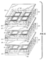
- FIG. 6 a fifth embodiment of the present invention suitable for direct-view, high-resolution, full-color display applications is shown.
- the polarizers between cells 32 and 34 and between cells 34 and 36, respectively, are not shown in order to avoid that cells 32 and 34 are hidden by those polarizers.
- Figure 5 illustrates this embodiment, in which each cell 32, 34 and 36 of the electronic subtractive color filter 30 contains a high-density matrix of picture elements and control the transmission of impinging broad band light therethrough.
- each picture element contains an integral sample-and-hold device (e.g., a thin-film transistor) 61 along with the address conducting leads (not shown).
- This active-matrix addressed subtractive color display has many construction features in common with the active-matrix addressed liquid crystal color matrix display depicted in Figure 1B.
- the major advantage of this embodiment of the present invention is the much higher full-color image resolution achievable with the electronic subtractive color filter as compared to a spatial additive approach in which at least three primary colors (R,G,B) must be represented in the image plane for each image point.
- R,G,B primary colors
- parallax is a potential problem in high-resolution, direct-view applications.
- the approaches for eliminating or minimizing parallax described for the previous embodiment are also applicable to the present high-resolution configuration.
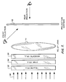
- the final embodiment of the present invention described herein utilizes the electronic subtractive color filter 30 as an image-forming, full-color, projection light valve.
- Image generation by the color filter 30 in response to incident radiation 38 can be for a low resolution image, in which case a direct multiplexed addressing technique is preferred, or for a high resolution image, in which case an active-matrix addressed configuration for pixel addressing in each guest/host liquid crystal cell 30 is typically preferred.
- Figure 7 illustrates a high-resolution implementation of the projection-mode embodiment of the present invention.
- the electronic subtractive color filter 30 functions as a full-color image-forming source which, when coupled to a broad band source of illumination 38 and relay lens 71 arrangement, is capable of projecting a full-color image on either a front- or rear-projection screen surface 72.
- the projection mode embodiment is particularly suitable for very high-resolution, full-color, large area display systems as well as for head-up display (HUD) and helmet-mounted display (HMD) applications.
- HUD head-up display
- HMD helmet-mounted display
- the full color image is collimated and then projected onto a transparent optical combiner which, via reflection of the projected image, superimposes the projected image with other visual images passing through the optical combiner.
- the HMD implementation is very similar to the HUD configuration, with the exception that the image source and optical combiner are now incorporated within a helmet worn by the display observer.
- the present invention is uniquely suited to provide the requisite resolution combined with full color capability for such devices.
- the capability for extremely high-resolution, full-color image generation in the projection mode of the present invention is primarily a function of the electronic subtractive color filter which yields full-color control at each individual picture element.
- the present invention employs a subtractive approach to color generation which enables full color control to be achieved at each individual image pixel or segment.
- an electronic color filter such that an image is formed by some other associated image forming device ⁇ e.g., a cathode-ray tube (CRT) or patterned image transilluminated by a light source ⁇
- the present invention can control the spectral emissions from the image forming source or impart color to an otherwise achromatic or monochromatic formed image.
- the subtractive liquid crystal displays of the present invention rely on the properties of the filter materials.
- the filter materials have controllable absorption characteristics, each of the three filter elements influencing (i.e., absorbing) radiation in a preselected portion of the spectrum and having a negligible influence on the remaining portion of the transmitted spectrum.
- the color components in a color chart combination determined by the filter characteristics, can be achieved at each pixel point when the impinging radiation (transmitted by the pixel filter) has the required spectral components.
- the directional nature of the transmitted radiation can be reduced, when a wider viewing angle is desirable, by placing a diffusion plate in front of the transmitted radiation.
- a full-color information display is created by using a single broad-band light or image source which passes emitted light through a stack composed of three thin liquid crystal cells.
- Each cell contains a different dichroic dye in a guest/host arrangement with the liquid crystal medium.
- magenta (M), cyan (C), and yellow (Y) dichroic dyes are used, which are the respective color complements of the R, G, and B primaries of additive color systems, however other dye combinations can be employed.
- the dichroic guest/host liquid cells each constitute an electronic color filter, which is switchable by the application of an appropriate voltage(s) across the two plates of the cell.
- the cell In one extreme state, the cell simply passes all spectral components of light, while in the other extreme state the spectral composition of light passing through the cell is altered by the particular dichroic dye such that the complementary color of the dye is blocked or subtracted from passage through the cell. Applied voltage levels in between those required to produce the extreme states result in gradations of the spectral shaping produced by the cell. Since spectral components of a broad-band source of light are subtracted (-R, -G, -B) rather than added (+R, +G, +B), a full-color electronic filter can be constructed by stacking three cells with an appropriately selected dye for each cell.
- a full-color information display is created with complete color control at each individual pixel.
- a broad-band image forming source i.e., a monochromatic display emitting white light
- a three-cell stack mounted in front of the imaging device a full-color information display is created in which the monochromatic image forming source controls image construction or detail and the three-cell liquid crystal stack serves as an electronically controlled color rendering filter.
- the present invention offers several advantages over existing approaches to the development of full-color information displays.
- First, the creation of a color display which uses subtractive color mixture enables full color control at every display pixel, eliminating degradations of potential resolution inherent to spatial additive approaches which require separate R, G, and B pixels to form each full-color image element.
- Second, a full-color low resolution display can be created without the high cost associated with spatial additive color display technologies which require a relatively high density (i.e., resolution) of primary color pixels just to accomplish the color mixture or synthesis function.
- Third, a color display using an electronically controlled color filter as described herein does not require frame-sequential operation and is thus not prone to the visual flicker and color image smear resulting from temporal color synthesis.
- the invention offers great flexibility for the design of color display systems used in a wide variety of applications, and can be configured as a simple electronic color filter for modifying the color of a monochromatic light or image source or as either a low- or high-resolution full-color information display.
- liquid crystal/dye components used in the liquid crystal cells suitable materials are commercially available, e.g., from EM Industries Inc., Advanced Chemical Division, 5 Skyline Drive, Hawthorne, N.Y. 10532.
Description
- The present invention relates generally to devices for the display of color information and, more particularly, to multi-color segmented or matrix-type displays in which a finite number of discretely addressable picture elements (pixels) are activated in appropriate combination to form a full-color image.
- In an article "Multicolored liquid crystal displays", published in Optical Engineering, Volume 23 (1984), May/June No. 3, pages 247 to 252, Tatsuo Uchida describes various types of color LCD's including the subtractive mixing and the additive mixing of color components. One of the displays uses twisted nematic cells with birefringent films between the cells together with polarizers in front of the first TN-cell and between the subsequent birefringent film and the second TN-cell. Subsequent polarizers show orthogonal polarization in relation to each other. In another embodiment this article describes a multilayer guest-host cell with a single polarizer in front of the first cell. As a preferred color LCD, the article describes a matrix LCD with microcolor layers inside the cell, where spatially distributed microcolor components are mixed visually similar to the mixing of the colors in a shadow mask color CRT.
- JP-A 60/169827 published as an abstract in Patent Abstracts of Japan, Vol. 10, No. 15 (P-422)(2072) on January 21, 1986, describes a liquid crystal projection device using a plurality of guest-host liquid crystal panels. The guest-host liquid crystal panels are inserted between an active matrix substrate on which thin-film transistors are integrated and an opposite substrate which has a transparent conductive film to form a panel.
- The three guest-host LC panels use pigments of three primary colors, i.e. yellow, cyan, and magenta, to form an optional color image. The panels are driven with the red, green and blue color video signals from a T.V. receiving unit.
- US-A 3 703 329 describes a color display system using a color filter according to the preamble of
claim 1. Each cell includes a solution consisting of a pleochroic dye in a nematic liquid crystal composition. The system illuminates the stack of cells with polarized white light. The solution of a pleochroic dye which is disolved in a nematic liquid crystal composition is contained between transparent support plates having transparent conductive coatings, respectively, on the inner surfaces thereof. In operation each of the conductive coatings is connected to a voltage source so as to separately control and vary the electric field applied across the liquid crystal solution of each liquid crystal cell. The specific composition in each of the three solutions is different from that of the others. - The present invention is characterized in
claim 1. The provision of polarizers between adjacent cells minimizes the facts of molecular birefringence in each cell and resulting chromatic shifts when viewing the filter off-axis. Preferred embodiments and details of the invention are described in the dependent claims. The invention also extends to electronically controlled color displays using such filters. - The basic elements of the subtractive color filter are three guest-host liquid crystal cells each containing a different dichroic guest dye {typically magenta (-G), cyan (-R), and yellow (-B) dyes} and stacked in registration along with associated structural components and optical components (e.g. polarizers and/or fiber-optic plates). The cells can include patterned electrodes {and for some applications integral sample-and-hold features such as thin film transistors (TFTs) at individual pixels} when the device is configured as either a low- or high-resolution full-color display, or a uniform electrode layer when the device is configured as a simple electronic color filter. When the device is configured as a color display, only a broad-band source of illumination is required for full-color image presentation. In the simple electronic color filter configuration, the device is used in conjunction with a broad-band image forming source, such as a cathode ray tube with white-emitting phosphor or a back-lit patterned illuminator with broad-band lamp, and serves as a spectrally selective light valve which modifies the color of the transmitted image.
- These and other features of the present invention will be understood upon reading of the following description along with the drawings.
- The rationale and preferred embodiment(s) of the present invention are illustrated in the attached drawings wherein:
- Figures 1A and 1B show two existing approaches for producing full-color images using the spatial-additive method of color synthesis: the shadow-mask color cathode ray tube (1A) and the active-matrix addressed liquid crystal display panel with R-G-B color filter array (1B).
- Figure 2 is a diagram of an electronic color filter using subtractive color mixture via three stacked guest/host cells with yellow, cyan, and magenta dichroic guest dyes.
- Figures 3A and 3B illustrate the control of color generation by an electronic subtractive color filter according to the invention for the colors red, green, blue, and yellow, respectively.
- Figure 4A is a diagram of an electronic subtractive color filter coupled to a symbol or character mask to create a static information display with full-color capability.
- Figure 4B is a diagram of an electronic subtractive color filter coupled to a broad-band, light-emitting image source to create a dynamic information display with full-color capability.
- Figure 5 shows a full-color alphanumeric display constructed with an integral electronic subtractive color filter.
- Figure 6 is a diagram of a 3-cell electronic subtractive color filter using a thin-film transistor active-matrix substrate in each cell to produce a full-color, high-resolution information display.
- Figure 7 is a diagram of an active-matrix addressed electronic subtractive color filter coupled to a projection optical system to produce a full-color, high-resolution projection display in both a front-projection and rear-projection configuration.
- Figures 1A and 1B illustrate two commonplace embodiments of spatial-additive color information displays. Referring first to Figure 1A, the typical shadow-mask
cathode ray tube 100 such as is used in commercial color television receivers and is the predominant device for color information display, is shown. Full color is achieved with the shadow-mask color cathode ray tube by the spatial integration of luminous emissions from closely-spaced R, G, andB phosphor dots 106, each of which is excited by an associatedelectron beam 102. The phosphor dots are positioned on the cathoderay tube face 104. Theelectron beams 102 are generated by a plurality of electron guns. The R, G andB phosphor dots 106 are arranged inpixel groups 105. Theelectron beams 102 exciting each phosphor dot of apixel group 105 pass through an aperture associated with eachpixel group 105 in theshadow mask 103. Note that the spatial integration of chromatic information is performed by the observer's eye and not the display device, thus requiring the display device to possess sufficient resolution such that the individual primary color elements are not individually resolvable by the eye of the observer. - Referring next to Figure 1B, another full-color display device which relies on spatial-additive color synthesis, is shown. This display is generally referred to as a active-matrix addressed liquid crystal color matrix display. While the basic principles of image formation and color mixture are the same as those used in the shadow-mask color cathode ray tube, the liquid crystal
color matrix display 120 employs a liquid crystal material which serves as an electronically-controlled light valve at each picture element to individually gate incident light through a micro-layer of color filters (typically R, G, and B).Back light 130 is transmitted through polarizingmaterial 127. The back light is then transmitted through theglass substrate 126 upon which are positionedthin film transistors 128.Liquid crystal material 125 is contained betweenglass substrate 126 and common (transparent)electrode 123. Associated with eachthin film transistor 128 is afilter 124. Thethin film transistor 128 controls the intensity of light transmitted through the associatedfilter 124. Three filters (R, G and B) 128 form an image pixel. The filtered light is then transmitted throughglass substrate 122 and polarizingunit 121. - Figure 2 shows an electronically-controlled
subtractive color filter 20 as known from Figure 2 of US-A-3703329 and Figure 3 of the T.Uchida article published in Optical Engineering. The elements include three guest/host liquid crystal cells each containing a different dichroic guest dye {typically a magenta dye (-G) cell 23, a cyan dye (-R)cell 22 and a yellow dye (-B) cell 21} and aligned in serial registration along with associated structural and optical components. The dichroic dye guest materials are attached to the liquid crystal host molecules in such a manner that, as the host molecular orientation aligns with respect to the applied electric field, so does the dye guest. The guest/host medium is contained between glass or plastic polymer plates and sealed by epoxy or thermoplastics. Depending upon the cell surface alignment and the liquid crystal materials used, the resulting guest/host medium can be one of several types: a) the single polarizer type (shown in Figure 2); b) the White-Taylor mode type; c) the phase change guest/host type; or d) the positive contrast negative anisotropic dielectric type. Guest/host medium types b, c, and d do not require a polarizer between the guest/host cell(s) and incident light, whereas type (a) requires a polarizingunit 21 oriented along the same direction as the liquid crystal host direction. The guest/host liquid crystal cells can be constructed with positive anisotropic liquid crystal materials such that the liquid crystal guest/host cells are selectively spectrally absorbing in the off state and become optically clear as a voltage is applied to the cell. The host liquid crystal material may be of the nematic, cholesteric, or smectic types. For positive anisotropic nematic and smectic hosts, a homogeneous molecular alignment to the cell surfaces is preferred. The guest/host liquid crystal cells can also be constructed with negative nematic anisotropic hosts and homeotropic molecular alignment. The guest host liquid crystal cells would then be optically clear in the off state and selectively spectrally absorbing in the on state. These host materials generally have higher voltage requirements and are not as readily available as "positive" nematic materials. - Figure 2 also illustrates the basic principles of operation of an electronically controlled subtractive color filter. As can be seen, broad-band incident light 29 from a broad-band source is first passed through a polarization layer and then sequentially through the three sequentially aligned guest/host
liquid crystal cells 20. Depending upon the guest dyes utilized and the voltage applied to each cell, the chromaticity (color) and luminance of the light emerging from the sequentially-aligned guest/host cells 20 can be completely controlled. - Referring next to Figure 3A and Figure 3B wherein anisotropic guest host dye cells with homogeneous molecular alignment are stacked, the operation of an electronically controlled subtractive color filter according to the invention is illustrated producing the colors red, green, blue, and yellow, respectively. Incident (white and unpolarized) light 38 impinges on polarizing
plate 31 and is transmitted therethrough to impinge oncell 1 32 having yellow dye material incorporated therein.Cell 1 32 includes afirst glass substrate 32A and asecond glass substrate 32C enclosing guest/host medium 32B. The light transmitted throughcell 1 32 is transmitted throughpolarizing plate 33 having an axis of polarization parallel to the axis of polarization of polarizingplate 31. After transmission throughpolarizing plate 33, the light is transmitted throughcell 2 34.Cell 2 34 has cyan dye material incorporated therein.Cell 2 34 is comprised ofglass substrate 34A andglass substrate 34C enclosing guest/host medium 34B. The light transmitted throughcell 2 34 is transmitted throughpolarizing plate 35, polarizingplate 35 having an axis of polarization parallel to the axis of polarization of polarizingplate 31. The light transmitted throughpolarizing plate 35 is applied tocell 3 36.Cell 3 36 has a magenta dye incorporated therein and hasglass substrate 36A andglass substrate 36C enclosing guest/host medium 36B. The light transmitted thoughcell 3 36 is the emerginglight 39 which will be polarized. (It will be clear thatcell 1 32,cell 2 34 andcell 3 36 each can have a multiplicity of independently addressable pixel points, the pixel points for each cell aligned with related points for the other two cells.) Referring next to Figure 3B, the configuration of thefilter 30 to provide selected colors is shown. Whencell 1 32 (with yellow dye) is off or absorbing,cell 2 34 (with cyan dye) is on or transmitting andcell 3 36 (with magenta dye) is off or absorbing, then the transmitted light will be red. Figure 3B illustrates the liquid crystal cell states that provide green, blue and yellow emerging light. It will be clear that the configurations and colors illustrated in Figure 3B constitute only a limited set of the colors and luminance gradations achievable with the present invention. Also note that the subtractive color filter construction shown in Figure 3A (as well as Figures 4 and 5) contains a polarizer behind each component guest/host liquid crystal cell. This particular type of filter construction has been found to operate effectively for direct-view display applications in which a wide viewing angle is desired. The polarization of light prior to passage through each cell minimizes the effects of molecular birefringence in each cell and resulting chromatic shifts when viewed off-axis. The off-axis chromatic shifts resulting from molecular birefringence can alternately be minimized or eliminated by the use of liquid crystal host and dye guest materials possessing very low molecular birefringence, thereby providing good off-axis color performance and higher luminance throughput than is possible by the use of a maximum of one polarization layer. The effects of molecular birefringence and viewing parallax are of no consequence in projection applications of the electronic subtractive color filter. - The preferred embodiment and principles of operation of the basic subtractive color filter of the present invention having been described above, the embodiment(s) of several forms of full-color information display devices (as well as a unique application for electronic spectral shaping of light sources), which employ the electronic subtractive color filter, can now be considered. Six embodiments of the present invention will be described. The first three embodiments utilize the electronic subtractive color filter as an integral component which is coupled to a monochromatic image forming source, thereby imparting full color capability to an otherwise monochromatic display device. The last three embodiments incorporate the function of image formation within the color filter stack itself, enabling the creation of both direct-view and projection-mode full-color information displays of either high or low resolution with the simple addition of a broad-band source of illumination. Another prior reference to the use of subtractive color mixture, at least in theory or concept, has been mentioned within the context of potential application to direct-view, full-color information displays (T. Uchida, "Color LCDs: Technological Developments", Japan Display, 1983, pp. 202-205). In this reference it is stated that subtractive color technology is potentially suitable only for low-resolution, direct-view display applications, and that only the active-matrix addressed liquid crystal color matrix display (as described in Figure 1b) is promising for practical use.
- The first embodiment of the present invention is depicted in Figure 4A, wherein the electronic
subtractive color filter 30 receives light from a broad-band source passing through a static alphanumeric character orsymbol mask 41 before being transmitted through thefilter 30. In this configuration, the present invention serves to impart full color control to an otherwise monochromatic display of information. This embodiment is particularly useful for illuminated annunciators and control actuators (e.g., push-buttons) with illuminated legends, where the addition of color coding can provide supplementary information to the static image. - A second and related embodiment of the electronic subtractive color filter receives light from the source of illumination and controls the color temperature or otherwise shapes the spectrum of the source of illumination. This embodiment is particularly applicable to aircraft cockpit panels and ship-board control panels, where it is highly desirable to maintain a constant color appearance of light sources and illuminated annunciators under all ambient lighting and panel dimming conditions. In this manner, the inherent decrease in color temperature associated with the voltage-controlled dimming of tungsten light sources can be offset or compensated for by the present invention. Within this context, the electronically-controlled subtractive color filter can provide automatic spectral shaping of cockpit light sources so as to render them night-vision-goggle compatible. The present invention thus permits the spectral output characteristics of sources of illumination to be automatically switched or optimized for both daytime and night/night-vision-goggle compatible operations.
- The third embodiment of the present invention is illustrated in Figure 4B, in which the electronic subtractive color filter is placed between a broad-band, light-emitting image source (e.g., a monochrome cathode ray tube) 42 and an observer. In this implementation, the
image source 42 provides dynamic, monochromatic image generation and the subtractive color filter imparts color to the image as it passes through the stack of guest/hostliquid crystal cells 30. The most basic implementation of this third embodiment would provide only for switching the color of the entire image. Multiple colors within the same image would not be possible, and therefore the device would not be suitable for color video applications. However, the electronic subtractive color filter can be operated in a frame-sequential mode such that red, green, and blue image components are produced sequentially in time and integrated by the observer's eyes. This mode of operation would allow a complete multi-color image to be generated and is potentially suitable for color video imaging. - Referring next to Figure 5, a fourth embodiment of the present invention comprising a direct-view, low-resolution color display, in which the image forming source is integral to the electronic subtractive color filter, is shown. The basic color filter unit is similar to that described in Figure 3 wherein three aligned
polarizing plates cells transparent electrodes 51 deposited on one of the glass (or plastic) plates of each guest/host liquid crystal cell. Conducting leads 52 are used to couple theelectrodes 51 to a voltage source (not shown). The other plate of each cell contains asimple backplane electrode 53. When a voltage is imposed across each cell, the liquid crystal material and guest dichroic dye switch only in the area under the patterned electrode. In order to achieve full-color, the three cells must be carefully aligned such that filtered light transmitted through the patterned areas of one cell sequentially passes through the corresponding patterned areas of the next sequential cell. A potential problem for this implementation occurs with respect to off-axis viewing or parallax. Image mis-registration due to parallax between layers of the three-cell stack can be minimized or functionally eliminated by the use of very thin glass or plastic plates for guest/hostliquid crystal cell - The preferred embodiment of the electronic subtractive color filter for direct-view, low-resolution color display applications, as described in the preceding paragraph, is particularly suitable for full-color alphanumeric and low-resolution graphics applications. A major advantage of this technical approach is elimination of the need for high pixel density (which is required to accommodate spatial color synthesis) resulting in a relatively simple, low-cost, full-color information display for those applications requiring only low to moderate image resolution. The low pixel density required for this display implementation allows the use of simple multiplexed pixel addressing and voltage drive techniques.
- Referring next to Figure 6, a fifth embodiment of the present invention suitable for direct-view, high-resolution, full-color display applications is shown. In the Figure the polarizers between
cells cells cells cell subtractive color filter 30 contains a high-density matrix of picture elements and control the transmission of impinging broad band light therethrough. In turn, each picture element contains an integral sample-and-hold device (e.g., a thin-film transistor) 61 along with the address conducting leads (not shown). This active-matrix addressed subtractive color display has many construction features in common with the active-matrix addressed liquid crystal color matrix display depicted in Figure 1B. However, the major advantage of this embodiment of the present invention is the much higher full-color image resolution achievable with the electronic subtractive color filter as compared to a spatial additive approach in which at least three primary colors (R,G,B) must be represented in the image plane for each image point. As with the low-resolution, direct view configuration described with reference to Figure 5, parallax is a potential problem in high-resolution, direct-view applications. The approaches for eliminating or minimizing parallax described for the previous embodiment are also applicable to the present high-resolution configuration. - Referring next to Figure 7, the final embodiment of the present invention described herein utilizes the electronic
subtractive color filter 30 as an image-forming, full-color, projection light valve. Image generation by thecolor filter 30 in response toincident radiation 38 can be for a low resolution image, in which case a direct multiplexed addressing technique is preferred, or for a high resolution image, in which case an active-matrix addressed configuration for pixel addressing in each guest/hostliquid crystal cell 30 is typically preferred. Figure 7 illustrates a high-resolution implementation of the projection-mode embodiment of the present invention. In this embodiment, the electronicsubtractive color filter 30 functions as a full-color image-forming source which, when coupled to a broad band source ofillumination 38 andrelay lens 71 arrangement, is capable of projecting a full-color image on either a front- or rear-projection screen surface 72. The projection mode embodiment is particularly suitable for very high-resolution, full-color, large area display systems as well as for head-up display (HUD) and helmet-mounted display (HMD) applications. For a HUD system, the full color image is collimated and then projected onto a transparent optical combiner which, via reflection of the projected image, superimposes the projected image with other visual images passing through the optical combiner. The HMD implementation is very similar to the HUD configuration, with the exception that the image source and optical combiner are now incorporated within a helmet worn by the display observer. In that both HUD and HMD systems require extremely high image resolution, the present invention is uniquely suited to provide the requisite resolution combined with full color capability for such devices. The capability for extremely high-resolution, full-color image generation in the projection mode of the present invention is primarily a function of the electronic subtractive color filter which yields full-color control at each individual picture element. - The present invention employs a subtractive approach to color generation which enables full color control to be achieved at each individual image pixel or segment. When used as an electronic color filter, such that an image is formed by some other associated image forming device {e.g., a cathode-ray tube (CRT) or patterned image transilluminated by a light source}, the present invention can control the spectral emissions from the image forming source or impart color to an otherwise achromatic or monochromatic formed image.
- The subtractive liquid crystal displays of the present invention rely on the properties of the filter materials. The filter materials have controllable absorption characteristics, each of the three filter elements influencing (i.e., absorbing) radiation in a preselected portion of the spectrum and having a negligible influence on the remaining portion of the transmitted spectrum. By appropriate selection of the filter materials, the color components in a color chart combination, determined by the filter characteristics, can be achieved at each pixel point when the impinging radiation (transmitted by the pixel filter) has the required spectral components. The directional nature of the transmitted radiation can be reduced, when a wider viewing angle is desirable, by placing a diffusion plate in front of the transmitted radiation.
- Using subtractive color mixture, a full-color information display is created by using a single broad-band light or image source which passes emitted light through a stack composed of three thin liquid crystal cells. Each cell contains a different dichroic dye in a guest/host arrangement with the liquid crystal medium. Typically, magenta (M), cyan (C), and yellow (Y) dichroic dyes are used, which are the respective color complements of the R, G, and B primaries of additive color systems, however other dye combinations can be employed. The dichroic guest/host liquid cells each constitute an electronic color filter, which is switchable by the application of an appropriate voltage(s) across the two plates of the cell. In one extreme state, the cell simply passes all spectral components of light, while in the other extreme state the spectral composition of light passing through the cell is altered by the particular dichroic dye such that the complementary color of the dye is blocked or subtracted from passage through the cell. Applied voltage levels in between those required to produce the extreme states result in gradations of the spectral shaping produced by the cell. Since spectral components of a broad-band source of light are subtracted (-R, -G, -B) rather than added (+R, +G, +B), a full-color electronic filter can be constructed by stacking three cells with an appropriately selected dye for each cell. Given a broad-band light source and a three-cell stack incorporating a pixel addressing mechanism in each of the cells, a full-color information display is created with complete color control at each individual pixel. Alternatively, given a broad-band image forming source (i.e., a monochromatic display emitting white light) and a three-cell stack mounted in front of the imaging device, a full-color information display is created in which the monochromatic image forming source controls image construction or detail and the three-cell liquid crystal stack serves as an electronically controlled color rendering filter.
- The present invention offers several advantages over existing approaches to the development of full-color information displays. First, the creation of a color display which uses subtractive color mixture enables full color control at every display pixel, eliminating degradations of potential resolution inherent to spatial additive approaches which require separate R, G, and B pixels to form each full-color image element. Second, a full-color low resolution display can be created without the high cost associated with spatial additive color display technologies which require a relatively high density (i.e., resolution) of primary color pixels just to accomplish the color mixture or synthesis function. Third, a color display using an electronically controlled color filter as described herein does not require frame-sequential operation and is thus not prone to the visual flicker and color image smear resulting from temporal color synthesis. Finally, the invention offers great flexibility for the design of color display systems used in a wide variety of applications, and can be configured as a simple electronic color filter for modifying the color of a monochromatic light or image source or as either a low- or high-resolution full-color information display.
- With respect to the liquid crystal/dye components used in the liquid crystal cells, suitable materials are commercially available, e.g., from EM Industries Inc., Advanced Chemical Division, 5 Skyline Drive, Hawthorne, N.Y. 10532.
Claims (10)
- A color filter for controlling transmission of applied light to provide a selected output color image, comprising:a) a first filter (32) including a first dye material cell (32B) having an electric field dependent absorption coefficient in a first preselected spectral range, and first electrodes positioned to apply an electric field to said first dye material;b) a second filter (34) including a second dye material cell (34B) having an electric field dependent absorption coefficient in a second preselected spectral range, and second electrodes positioned to apply an electric field to said second dye material;c) a first polarizer (31) provided at the light input side of said first dye material cell (32B), characterized byd) a second polarizer (33) provided between said first and second dye material cells (32B, 34B).
- The color filter of claim 1, characterized by a third filter (36) includinga) a third dye material cell (36B) having an electric field dependent absorption coefficient in a third preselected spectral range, and third electrodes positioned to apply an electric field to said third dye material; andb) a third polarizer (35) provided between said second and third dye material cells (34B, 36B).
- The color filter of claim 1 or 2, characterized in that said first, second and third dye materials (32B, 34B, 36B) include a dichroic guest dye coupled to a liquid crystal.
- The color filter of one of the preceding claims, characterized in that said color filter (30) includes a plurality of aligned sets of first, second and third dye material cells (32, 34, 36), with each set of cells controlling transmission of light in a preselected region of said filter.
- The color filter according to one of the preceding claims, characterized in that all cell polarizers (31, 33, 35) have the same direction of polarisation.
- An electronically controlled color display comprising a color filter according to one of the preceding claims, characterized by a broad band source (41, 42) of radiation arranged to illuminate said first polarizer (31).
- The display of claim 6, characterized in that each of said dye material cells (32B, 34B, 36B) is a segment of a segmented color display.
- The display of claim 6, characterized in that each of said dye material cells (32B, 34B, 36B) is a pixel (61) of a matrix color display.
- The display of claim 8, characterized in that each pixel includes an integral thin film transistor (61).
- The color filter or display according to one of the preceding claims, characterized in that said first, second and third dye materials include a positive anisotropic nematic or smectic material.
Applications Claiming Priority (2)
| Application Number | Priority Date | Filing Date | Title |
|---|---|---|---|
| US178949 | 1988-04-07 | ||
| US07/178,949 US5032007A (en) | 1988-04-07 | 1988-04-07 | Apparatus and method for an electronically controlled color filter for use in information display applications |
Publications (3)
| Publication Number | Publication Date |
|---|---|
| EP0336351A2 EP0336351A2 (en) | 1989-10-11 |
| EP0336351A3 EP0336351A3 (en) | 1990-08-01 |
| EP0336351B1 true EP0336351B1 (en) | 1994-08-24 |
Family
ID=22654572
Family Applications (1)
| Application Number | Title | Priority Date | Filing Date |
|---|---|---|---|
| EP89105846A Expired - Lifetime EP0336351B1 (en) | 1988-04-07 | 1989-04-04 | Controlled color filter for use in information display applications |
Country Status (5)
| Country | Link |
|---|---|
| US (1) | US5032007A (en) |
| EP (1) | EP0336351B1 (en) |
| JP (1) | JP2791952B2 (en) |
| CA (1) | CA1331060C (en) |
| DE (1) | DE68917628T2 (en) |
Cited By (9)
| Publication number | Priority date | Publication date | Assignee | Title |
|---|---|---|---|---|
| US6046716A (en) | 1996-12-19 | 2000-04-04 | Colorado Microdisplay, Inc. | Display system having electrode modulation to alter a state of an electro-optic layer |
| US6078303A (en) | 1996-12-19 | 2000-06-20 | Colorado Microdisplay, Inc. | Display system having electrode modulation to alter a state of an electro-optic layer |
| US7742124B2 (en) | 2001-04-20 | 2010-06-22 | Puredepth Limited | Optical retarder |
| US7742239B2 (en) | 2002-03-17 | 2010-06-22 | Puredepth Limited | Method to control point spread function of an image |
| US8146277B2 (en) | 2002-09-20 | 2012-04-03 | Puredepth Limited | Multi-view display |
| US8149353B2 (en) | 2001-10-11 | 2012-04-03 | Puredepth Limited | Visual display unit illumination |
| US8154691B2 (en) | 2000-11-17 | 2012-04-10 | Pure Depth Limited | Altering surfaces of display screens |
| US8416150B2 (en) | 2007-08-22 | 2013-04-09 | Igt | Method and system for determining a position for an interstital diffuser for use in a multi-layer display |
| US9137525B2 (en) | 2002-07-15 | 2015-09-15 | Pure Depth Limited | Multilayer video screen |
Families Citing this family (257)
| Publication number | Priority date | Publication date | Assignee | Title |
|---|---|---|---|---|
| DE388976T1 (en) * | 1989-03-28 | 1991-04-11 | In Focus Systems, Inc., Tualatin, Oreg., Us | COLOR DISPLAY. |
| US5050965A (en) * | 1989-09-01 | 1991-09-24 | In Focus Systems, Inc. | Color display using supertwisted nematic liquid crystal material |
| US5113272A (en) * | 1990-02-12 | 1992-05-12 | Raychem Corporation | Three dimensional semiconductor display using liquid crystal |
| US5206749A (en) * | 1990-12-31 | 1993-04-27 | Kopin Corporation | Liquid crystal display having essentially single crystal transistors pixels and driving circuits |
| US5751261A (en) * | 1990-12-31 | 1998-05-12 | Kopin Corporation | Control system for display panels |
| US5743614A (en) * | 1990-12-31 | 1998-04-28 | Kopin Corporation | Housing assembly for a matrix display |
| US6320568B1 (en) | 1990-12-31 | 2001-11-20 | Kopin Corporation | Control system for display panels |
| US5861929A (en) * | 1990-12-31 | 1999-01-19 | Kopin Corporation | Active matrix color display with multiple cells and connection through substrate |
| US5376979A (en) * | 1990-12-31 | 1994-12-27 | Kopin Corporation | Slide projector mountable light valve display |
| US5444557A (en) * | 1990-12-31 | 1995-08-22 | Kopin Corporation | Single crystal silicon arrayed devices for projection displays |
| US5661371A (en) * | 1990-12-31 | 1997-08-26 | Kopin Corporation | Color filter system for light emitting display panels |
| US5122887A (en) * | 1991-03-05 | 1992-06-16 | Sayett Group, Inc. | Color display utilizing twisted nematic LCDs and selective polarizers |
| JP2829149B2 (en) * | 1991-04-10 | 1998-11-25 | シャープ株式会社 | Liquid crystal display |
| US5565933A (en) * | 1992-06-08 | 1996-10-15 | Hughes-Jvc Technology Corporation | Color switching apparatus for liquid crystal light valve projector |
| JP3329887B2 (en) * | 1992-06-17 | 2002-09-30 | ゼロックス・コーポレーション | Two-path liquid crystal light valve color display |
| US5693421A (en) * | 1992-12-22 | 1997-12-02 | Dai Nippon Printing Co., Ltd. | Information recording medium and information recording and reproducing method |
| US5835074A (en) * | 1992-12-30 | 1998-11-10 | Advanced Displays Corporation | Method to change the viewing angle in a fixed liquid crystal display by changing the pre-tilt angle in the liquid crystal layer with a bias voltage |
| US5309169A (en) * | 1993-02-01 | 1994-05-03 | Honeywell Inc. | Visor display with fiber optic faceplate correction |
| US5548422A (en) * | 1993-06-28 | 1996-08-20 | In Focus Systems, Inc. | Notch filters with cholesteric polarizers with birefringent film and linear polarizer |
| US5661578A (en) * | 1993-07-27 | 1997-08-26 | Honeywell Inc. | Color liquid crystal display backlight system for night vision imaging system compatibility |
| JPH0772446A (en) * | 1993-09-01 | 1995-03-17 | Sharp Corp | Display system |
| US5594563A (en) * | 1994-05-31 | 1997-01-14 | Honeywell Inc. | High resolution subtractive color projection system |
| US5751385A (en) * | 1994-06-07 | 1998-05-12 | Honeywell, Inc. | Subtractive color LCD utilizing circular notch polarizers and including a triband or broadband filter tuned light source or dichroic sheet color polarizers |
| JPH0843760A (en) * | 1994-07-29 | 1996-02-16 | Olympus Optical Co Ltd | Eyeball projection type video display device |
| US5615032A (en) * | 1994-08-12 | 1997-03-25 | Kaiser Aerospace And Electronics Corporation | Nightvision compatible display with electrically activated infrared filter |
| SG47360A1 (en) * | 1994-11-14 | 1998-04-17 | Hoffmann La Roche | Colour display with serially-connected lc filters |
| US5999240A (en) | 1995-05-23 | 1999-12-07 | Colorlink, Inc. | Optical retarder stack pair for transforming input light into polarization states having saturated color spectra |
| US6183091B1 (en) * | 1995-04-07 | 2001-02-06 | Colorlink, Inc. | Color imaging systems and methods |
| US5751384A (en) * | 1995-05-23 | 1998-05-12 | The Board Of Regents Of The University Of Colorado | Color polarizers for polarizing an additive color spectrum along a first axis and it's compliment along a second axis |
| US6252638B1 (en) | 1995-05-23 | 2001-06-26 | Colorlink, Inc. | Color controllable illumination device, indicator lights, transmissive windows and color filters employing retarder stacks |
| US5822021A (en) * | 1996-05-14 | 1998-10-13 | Colorlink, Inc. | Color shutter liquid crystal display system |
| US6707516B1 (en) | 1995-05-23 | 2004-03-16 | Colorlink, Inc. | Single-panel field-sequential color display systems |
| US6882384B1 (en) | 1995-05-23 | 2005-04-19 | Colorlink, Inc. | Color filters and sequencers using color selective light modulators |
| US5539552A (en) * | 1995-04-20 | 1996-07-23 | Aerospace Display Systems | Protective member for display system having 99% UV light blocking ability and improved thermal coefficient of expansion |
| US6417892B1 (en) | 1995-05-23 | 2002-07-09 | Colorlink, Inc. | Color filters, sequencers and displays using color selective light modulators |
| US6049367A (en) * | 1995-05-23 | 2000-04-11 | Colorlink, Inc. | Polarization manipulating device modulator with retarder stack which preconditions light for modulation and isotropic states |
| US6273571B1 (en) | 1995-05-23 | 2001-08-14 | Colorlink, Inc. | Display architectures using an electronically controlled optical retarder stack |
| US5929946A (en) * | 1995-05-23 | 1999-07-27 | Colorlink, Inc. | Retarder stack for preconditioning light for a modulator having modulation and isotropic states of polarization |
| JPH08328031A (en) * | 1995-06-02 | 1996-12-13 | Sharp Corp | Full-color liquid crystal display device and its production |
| JPH095745A (en) * | 1995-06-07 | 1997-01-10 | Xerox Corp | Optical-fiber face plate of color liquid crystal display device |
| WO1997001792A1 (en) * | 1995-06-26 | 1997-01-16 | Honeywell Inc. | Full color display of subtractive color type |
| JPH0926596A (en) * | 1995-07-13 | 1997-01-28 | Sharp Corp | Liquid crystal display device and its production |
| JP3728679B2 (en) * | 1996-10-16 | 2005-12-21 | フジノン株式会社 | Color separation optical system |
| US5920298A (en) * | 1996-12-19 | 1999-07-06 | Colorado Microdisplay, Inc. | Display system having common electrode modulation |
| JP3974217B2 (en) | 1997-04-02 | 2007-09-12 | シャープ株式会社 | Liquid crystal display panel and liquid crystal display device |
| JP3335998B2 (en) | 1998-02-20 | 2002-10-21 | ディープ ヴィデオ イメージング リミテッド | Multi-layer display device |
| KR20010015442A (en) * | 1999-07-27 | 2001-02-26 | 카나야 오사무 | Liquid crystal display and method of producing a liquid crystal display |
| US6830831B2 (en) * | 2001-06-29 | 2004-12-14 | University Of Hull | Light emitter for a display |
| US7250930B2 (en) * | 2003-02-07 | 2007-07-31 | Hewlett-Packard Development Company, L.P. | Transparent active-matrix display |
| JP4654573B2 (en) * | 2003-10-09 | 2011-03-23 | セイコーエプソン株式会社 | Screen, projector system, and image display method for projector system |
| DE102005008594B4 (en) * | 2004-02-23 | 2012-08-23 | Optrex Europe Gmbh | Display with a self-luminous display |
| CN1993608A (en) * | 2004-07-30 | 2007-07-04 | 夏普株式会社 | Method and apparatus for inspecting color filter |
| CN101116133B (en) | 2004-12-23 | 2014-02-05 | 杜比实验室特许公司 | Wide color gamut displays |
| US7403180B1 (en) * | 2007-01-29 | 2008-07-22 | Qualcomm Mems Technologies, Inc. | Hybrid color synthesis for multistate reflective modulator displays |
| JP2011529581A (en) * | 2008-07-29 | 2011-12-08 | トムソン ライセンシング | Display characterization by filtering |
| US9577642B2 (en) | 2009-04-14 | 2017-02-21 | Monolithic 3D Inc. | Method to form a 3D semiconductor device |
| US8258810B2 (en) | 2010-09-30 | 2012-09-04 | Monolithic 3D Inc. | 3D semiconductor device |
| US9509313B2 (en) | 2009-04-14 | 2016-11-29 | Monolithic 3D Inc. | 3D semiconductor device |
| US8754533B2 (en) | 2009-04-14 | 2014-06-17 | Monolithic 3D Inc. | Monolithic three-dimensional semiconductor device and structure |
| US8378715B2 (en) | 2009-04-14 | 2013-02-19 | Monolithic 3D Inc. | Method to construct systems |
| US8373439B2 (en) | 2009-04-14 | 2013-02-12 | Monolithic 3D Inc. | 3D semiconductor device |
| US8362800B2 (en) | 2010-10-13 | 2013-01-29 | Monolithic 3D Inc. | 3D semiconductor device including field repairable logics |
| US8362482B2 (en) | 2009-04-14 | 2013-01-29 | Monolithic 3D Inc. | Semiconductor device and structure |
| US7986042B2 (en) | 2009-04-14 | 2011-07-26 | Monolithic 3D Inc. | Method for fabrication of a semiconductor device and structure |
| US8427200B2 (en) | 2009-04-14 | 2013-04-23 | Monolithic 3D Inc. | 3D semiconductor device |
| US8395191B2 (en) | 2009-10-12 | 2013-03-12 | Monolithic 3D Inc. | Semiconductor device and structure |
| US8058137B1 (en) | 2009-04-14 | 2011-11-15 | Monolithic 3D Inc. | Method for fabrication of a semiconductor device and structure |
| US8384426B2 (en) | 2009-04-14 | 2013-02-26 | Monolithic 3D Inc. | Semiconductor device and structure |
| US9711407B2 (en) | 2009-04-14 | 2017-07-18 | Monolithic 3D Inc. | Method of manufacturing a three dimensional integrated circuit by transfer of a mono-crystalline layer |
| US8405420B2 (en) | 2009-04-14 | 2013-03-26 | Monolithic 3D Inc. | System comprising a semiconductor device and structure |
| US8669778B1 (en) | 2009-04-14 | 2014-03-11 | Monolithic 3D Inc. | Method for design and manufacturing of a 3D semiconductor device |
| US8456586B2 (en) | 2009-06-11 | 2013-06-04 | Apple Inc. | Portable computer display structures |
| US11374118B2 (en) | 2009-10-12 | 2022-06-28 | Monolithic 3D Inc. | Method to form a 3D integrated circuit |
| US8742476B1 (en) | 2012-11-27 | 2014-06-03 | Monolithic 3D Inc. | Semiconductor device and structure |
| US8450804B2 (en) | 2011-03-06 | 2013-05-28 | Monolithic 3D Inc. | Semiconductor device and structure for heat removal |
| US9099424B1 (en) | 2012-08-10 | 2015-08-04 | Monolithic 3D Inc. | Semiconductor system, device and structure with heat removal |
| US10043781B2 (en) | 2009-10-12 | 2018-08-07 | Monolithic 3D Inc. | 3D semiconductor device and structure |
| US11018133B2 (en) | 2009-10-12 | 2021-05-25 | Monolithic 3D Inc. | 3D integrated circuit |
| US10157909B2 (en) | 2009-10-12 | 2018-12-18 | Monolithic 3D Inc. | 3D semiconductor device and structure |
| US8536023B2 (en) | 2010-11-22 | 2013-09-17 | Monolithic 3D Inc. | Method of manufacturing a semiconductor device and structure |
| US10366970B2 (en) | 2009-10-12 | 2019-07-30 | Monolithic 3D Inc. | 3D semiconductor device and structure |
| US10388863B2 (en) | 2009-10-12 | 2019-08-20 | Monolithic 3D Inc. | 3D memory device and structure |
| US8148728B2 (en) | 2009-10-12 | 2012-04-03 | Monolithic 3D, Inc. | Method for fabrication of a semiconductor device and structure |
| US8476145B2 (en) | 2010-10-13 | 2013-07-02 | Monolithic 3D Inc. | Method of fabricating a semiconductor device and structure |
| US10910364B2 (en) | 2009-10-12 | 2021-02-02 | Monolitaic 3D Inc. | 3D semiconductor device |
| US8581349B1 (en) | 2011-05-02 | 2013-11-12 | Monolithic 3D Inc. | 3D memory semiconductor device and structure |
| US10354995B2 (en) | 2009-10-12 | 2019-07-16 | Monolithic 3D Inc. | Semiconductor memory device and structure |
| US8408780B2 (en) * | 2009-11-03 | 2013-04-02 | Apple Inc. | Portable computer housing with integral display |
| US8743309B2 (en) | 2009-11-10 | 2014-06-03 | Apple Inc. | Methods for fabricating display structures |
| US8541819B1 (en) | 2010-12-09 | 2013-09-24 | Monolithic 3D Inc. | Semiconductor device and structure |
| US9099526B2 (en) | 2010-02-16 | 2015-08-04 | Monolithic 3D Inc. | Integrated circuit device and structure |
| US8492886B2 (en) | 2010-02-16 | 2013-07-23 | Monolithic 3D Inc | 3D integrated circuit with logic |
| US8461035B1 (en) | 2010-09-30 | 2013-06-11 | Monolithic 3D Inc. | Method for fabrication of a semiconductor device and structure |
| US8026521B1 (en) | 2010-10-11 | 2011-09-27 | Monolithic 3D Inc. | Semiconductor device and structure |
| US8298875B1 (en) | 2011-03-06 | 2012-10-30 | Monolithic 3D Inc. | Method for fabrication of a semiconductor device and structure |
| US8373230B1 (en) | 2010-10-13 | 2013-02-12 | Monolithic 3D Inc. | Method for fabrication of a semiconductor device and structure |
| US9219005B2 (en) | 2011-06-28 | 2015-12-22 | Monolithic 3D Inc. | Semiconductor system and device |
| US8901613B2 (en) | 2011-03-06 | 2014-12-02 | Monolithic 3D Inc. | Semiconductor device and structure for heat removal |
| US8642416B2 (en) | 2010-07-30 | 2014-02-04 | Monolithic 3D Inc. | Method of forming three dimensional integrated circuit devices using layer transfer technique |
| US10217667B2 (en) | 2011-06-28 | 2019-02-26 | Monolithic 3D Inc. | 3D semiconductor device, fabrication method and system |
| US9953925B2 (en) | 2011-06-28 | 2018-04-24 | Monolithic 3D Inc. | Semiconductor system and device |
| US8163581B1 (en) | 2010-10-13 | 2012-04-24 | Monolith IC 3D | Semiconductor and optoelectronic devices |
| US8273610B2 (en) | 2010-11-18 | 2012-09-25 | Monolithic 3D Inc. | Method of constructing a semiconductor device and structure |
| US11482440B2 (en) | 2010-12-16 | 2022-10-25 | Monolithic 3D Inc. | 3D semiconductor device and structure with a built-in test circuit for repairing faulty circuits |
| US10497713B2 (en) | 2010-11-18 | 2019-12-03 | Monolithic 3D Inc. | 3D semiconductor memory device and structure |
| US11315980B1 (en) | 2010-10-11 | 2022-04-26 | Monolithic 3D Inc. | 3D semiconductor device and structure with transistors |
| US11227897B2 (en) | 2010-10-11 | 2022-01-18 | Monolithic 3D Inc. | Method for producing a 3D semiconductor memory device and structure |
| US10290682B2 (en) | 2010-10-11 | 2019-05-14 | Monolithic 3D Inc. | 3D IC semiconductor device and structure with stacked memory |
| US11600667B1 (en) | 2010-10-11 | 2023-03-07 | Monolithic 3D Inc. | Method to produce 3D semiconductor devices and structures with memory |
| US11024673B1 (en) | 2010-10-11 | 2021-06-01 | Monolithic 3D Inc. | 3D semiconductor device and structure |
| US11257867B1 (en) | 2010-10-11 | 2022-02-22 | Monolithic 3D Inc. | 3D semiconductor device and structure with oxide bonds |
| US10896931B1 (en) | 2010-10-11 | 2021-01-19 | Monolithic 3D Inc. | 3D semiconductor device and structure |
| US11158674B2 (en) | 2010-10-11 | 2021-10-26 | Monolithic 3D Inc. | Method to produce a 3D semiconductor device and structure |
| US11018191B1 (en) | 2010-10-11 | 2021-05-25 | Monolithic 3D Inc. | 3D semiconductor device and structure |
| US8114757B1 (en) | 2010-10-11 | 2012-02-14 | Monolithic 3D Inc. | Semiconductor device and structure |
| US11469271B2 (en) | 2010-10-11 | 2022-10-11 | Monolithic 3D Inc. | Method to produce 3D semiconductor devices and structures with memory |
| US11605663B2 (en) | 2010-10-13 | 2023-03-14 | Monolithic 3D Inc. | Multilevel semiconductor device and structure with image sensors and wafer bonding |
| US11063071B1 (en) | 2010-10-13 | 2021-07-13 | Monolithic 3D Inc. | Multilevel semiconductor device and structure with waveguides |
| US11929372B2 (en) | 2010-10-13 | 2024-03-12 | Monolithic 3D Inc. | Multilevel semiconductor device and structure with image sensors and wafer bonding |
| US8283215B2 (en) | 2010-10-13 | 2012-10-09 | Monolithic 3D Inc. | Semiconductor and optoelectronic devices |
| US11043523B1 (en) | 2010-10-13 | 2021-06-22 | Monolithic 3D Inc. | Multilevel semiconductor device and structure with image sensors |
| US10679977B2 (en) | 2010-10-13 | 2020-06-09 | Monolithic 3D Inc. | 3D microdisplay device and structure |
| US11133344B2 (en) | 2010-10-13 | 2021-09-28 | Monolithic 3D Inc. | Multilevel semiconductor device and structure with image sensors |
| US11164898B2 (en) | 2010-10-13 | 2021-11-02 | Monolithic 3D Inc. | Multilevel semiconductor device and structure |
| US11437368B2 (en) | 2010-10-13 | 2022-09-06 | Monolithic 3D Inc. | Multilevel semiconductor device and structure with oxide bonding |
| US10833108B2 (en) | 2010-10-13 | 2020-11-10 | Monolithic 3D Inc. | 3D microdisplay device and structure |
| US11694922B2 (en) | 2010-10-13 | 2023-07-04 | Monolithic 3D Inc. | Multilevel semiconductor device and structure with oxide bonding |
| US9197804B1 (en) | 2011-10-14 | 2015-11-24 | Monolithic 3D Inc. | Semiconductor and optoelectronic devices |
| US11855100B2 (en) | 2010-10-13 | 2023-12-26 | Monolithic 3D Inc. | Multilevel semiconductor device and structure with oxide bonding |
| US11163112B2 (en) | 2010-10-13 | 2021-11-02 | Monolithic 3D Inc. | Multilevel semiconductor device and structure with electromagnetic modulators |
| US10998374B1 (en) | 2010-10-13 | 2021-05-04 | Monolithic 3D Inc. | Multilevel semiconductor device and structure |
| US10978501B1 (en) | 2010-10-13 | 2021-04-13 | Monolithic 3D Inc. | Multilevel semiconductor device and structure with waveguides |
| US11404466B2 (en) | 2010-10-13 | 2022-08-02 | Monolithic 3D Inc. | Multilevel semiconductor device and structure with image sensors |
| US11327227B2 (en) | 2010-10-13 | 2022-05-10 | Monolithic 3D Inc. | Multilevel semiconductor device and structure with electromagnetic modulators |
| US10943934B2 (en) | 2010-10-13 | 2021-03-09 | Monolithic 3D Inc. | Multilevel semiconductor device and structure |
| US11855114B2 (en) | 2010-10-13 | 2023-12-26 | Monolithic 3D Inc. | Multilevel semiconductor device and structure with image sensors and wafer bonding |
| US11869915B2 (en) | 2010-10-13 | 2024-01-09 | Monolithic 3D Inc. | Multilevel semiconductor device and structure with image sensors and wafer bonding |
| US8379458B1 (en) | 2010-10-13 | 2013-02-19 | Monolithic 3D Inc. | Semiconductor device and structure |
| US9143668B2 (en) | 2010-10-29 | 2015-09-22 | Apple Inc. | Camera lens structures and display structures for electronic devices |
| US8467177B2 (en) | 2010-10-29 | 2013-06-18 | Apple Inc. | Displays with polarizer windows and opaque masking layers for electronic devices |
| US11355380B2 (en) | 2010-11-18 | 2022-06-07 | Monolithic 3D Inc. | Methods for producing 3D semiconductor memory device and structure utilizing alignment marks |
| US11521888B2 (en) | 2010-11-18 | 2022-12-06 | Monolithic 3D Inc. | 3D semiconductor device and structure with high-k metal gate transistors |
| US11482439B2 (en) | 2010-11-18 | 2022-10-25 | Monolithic 3D Inc. | Methods for producing a 3D semiconductor memory device comprising charge trap junction-less transistors |
| US11804396B2 (en) | 2010-11-18 | 2023-10-31 | Monolithic 3D Inc. | Methods for producing a 3D semiconductor device and structure with memory cells and multiple metal layers |
| US11923230B1 (en) | 2010-11-18 | 2024-03-05 | Monolithic 3D Inc. | 3D semiconductor device and structure with bonding |
| US11121021B2 (en) | 2010-11-18 | 2021-09-14 | Monolithic 3D Inc. | 3D semiconductor device and structure |
| US11164770B1 (en) | 2010-11-18 | 2021-11-02 | Monolithic 3D Inc. | Method for producing a 3D semiconductor memory device and structure |
| US11901210B2 (en) | 2010-11-18 | 2024-02-13 | Monolithic 3D Inc. | 3D semiconductor device and structure with memory |
| US11495484B2 (en) | 2010-11-18 | 2022-11-08 | Monolithic 3D Inc. | 3D semiconductor devices and structures with at least two single-crystal layers |
| US11862503B2 (en) | 2010-11-18 | 2024-01-02 | Monolithic 3D Inc. | Method for producing a 3D semiconductor device and structure with memory cells and multiple metal layers |
| US11508605B2 (en) | 2010-11-18 | 2022-11-22 | Monolithic 3D Inc. | 3D semiconductor memory device and structure |
| US11784082B2 (en) | 2010-11-18 | 2023-10-10 | Monolithic 3D Inc. | 3D semiconductor device and structure with bonding |
| US11443971B2 (en) | 2010-11-18 | 2022-09-13 | Monolithic 3D Inc. | 3D semiconductor device and structure with memory |
| US11031275B2 (en) | 2010-11-18 | 2021-06-08 | Monolithic 3D Inc. | 3D semiconductor device and structure with memory |
| US11569117B2 (en) | 2010-11-18 | 2023-01-31 | Monolithic 3D Inc. | 3D semiconductor device and structure with single-crystal layers |
| US11004719B1 (en) | 2010-11-18 | 2021-05-11 | Monolithic 3D Inc. | Methods for producing a 3D semiconductor memory device and structure |
| US11615977B2 (en) | 2010-11-18 | 2023-03-28 | Monolithic 3D Inc. | 3D semiconductor memory device and structure |
| US11355381B2 (en) | 2010-11-18 | 2022-06-07 | Monolithic 3D Inc. | 3D semiconductor memory device and structure |
| US11735462B2 (en) | 2010-11-18 | 2023-08-22 | Monolithic 3D Inc. | 3D semiconductor device and structure with single-crystal layers |
| US11094576B1 (en) | 2010-11-18 | 2021-08-17 | Monolithic 3D Inc. | Methods for producing a 3D semiconductor memory device and structure |
| US11482438B2 (en) | 2010-11-18 | 2022-10-25 | Monolithic 3D Inc. | Methods for producing a 3D semiconductor memory device and structure |
| US11854857B1 (en) | 2010-11-18 | 2023-12-26 | Monolithic 3D Inc. | Methods for producing a 3D semiconductor device and structure with memory cells and multiple metal layers |
| US11107721B2 (en) | 2010-11-18 | 2021-08-31 | Monolithic 3D Inc. | 3D semiconductor device and structure with NAND logic |
| US11211279B2 (en) | 2010-11-18 | 2021-12-28 | Monolithic 3D Inc. | Method for processing a 3D integrated circuit and structure |
| US11610802B2 (en) | 2010-11-18 | 2023-03-21 | Monolithic 3D Inc. | Method for producing a 3D semiconductor device and structure with single crystal transistors and metal gate electrodes |
| US11018042B1 (en) | 2010-11-18 | 2021-05-25 | Monolithic 3D Inc. | 3D semiconductor memory device and structure |
| US8975670B2 (en) | 2011-03-06 | 2015-03-10 | Monolithic 3D Inc. | Semiconductor device and structure for heat removal |
| US10388568B2 (en) | 2011-06-28 | 2019-08-20 | Monolithic 3D Inc. | 3D semiconductor device and system |
| US8687399B2 (en) | 2011-10-02 | 2014-04-01 | Monolithic 3D Inc. | Semiconductor device and structure |
| US9029173B2 (en) | 2011-10-18 | 2015-05-12 | Monolithic 3D Inc. | Method for fabrication of a semiconductor device and structure |
| US9000557B2 (en) | 2012-03-17 | 2015-04-07 | Zvi Or-Bach | Semiconductor device and structure |
| US11088050B2 (en) | 2012-04-09 | 2021-08-10 | Monolithic 3D Inc. | 3D semiconductor device with isolation layers |
| US10600888B2 (en) | 2012-04-09 | 2020-03-24 | Monolithic 3D Inc. | 3D semiconductor device |
| US11694944B1 (en) | 2012-04-09 | 2023-07-04 | Monolithic 3D Inc. | 3D semiconductor device and structure with metal layers and a connective path |
| US11594473B2 (en) | 2012-04-09 | 2023-02-28 | Monolithic 3D Inc. | 3D semiconductor device and structure with metal layers and a connective path |
| US11410912B2 (en) | 2012-04-09 | 2022-08-09 | Monolithic 3D Inc. | 3D semiconductor device with vias and isolation layers |
| US11735501B1 (en) | 2012-04-09 | 2023-08-22 | Monolithic 3D Inc. | 3D semiconductor device and structure with metal layers and a connective path |
| US11616004B1 (en) | 2012-04-09 | 2023-03-28 | Monolithic 3D Inc. | 3D semiconductor device and structure with metal layers and a connective path |
| US11164811B2 (en) | 2012-04-09 | 2021-11-02 | Monolithic 3D Inc. | 3D semiconductor device with isolation layers and oxide-to-oxide bonding |
| US11881443B2 (en) | 2012-04-09 | 2024-01-23 | Monolithic 3D Inc. | 3D semiconductor device and structure with metal layers and a connective path |
| US8557632B1 (en) | 2012-04-09 | 2013-10-15 | Monolithic 3D Inc. | Method for fabrication of a semiconductor device and structure |
| US11476181B1 (en) | 2012-04-09 | 2022-10-18 | Monolithic 3D Inc. | 3D semiconductor device and structure with metal layers |
| US20130328942A1 (en) * | 2012-06-12 | 2013-12-12 | Stephen Chen | Head up display for a vehicle |
| US8574929B1 (en) | 2012-11-16 | 2013-11-05 | Monolithic 3D Inc. | Method to form a 3D semiconductor device and structure |
| US8686428B1 (en) | 2012-11-16 | 2014-04-01 | Monolithic 3D Inc. | Semiconductor device and structure |
| US11018116B2 (en) | 2012-12-22 | 2021-05-25 | Monolithic 3D Inc. | Method to form a 3D semiconductor device and structure |
| US11063024B1 (en) | 2012-12-22 | 2021-07-13 | Monlithic 3D Inc. | Method to form a 3D semiconductor device and structure |
| US11217565B2 (en) | 2012-12-22 | 2022-01-04 | Monolithic 3D Inc. | Method to form a 3D semiconductor device and structure |
| US11309292B2 (en) | 2012-12-22 | 2022-04-19 | Monolithic 3D Inc. | 3D semiconductor device and structure with metal layers |
| US11784169B2 (en) | 2012-12-22 | 2023-10-10 | Monolithic 3D Inc. | 3D semiconductor device and structure with metal layers |
| US8674470B1 (en) | 2012-12-22 | 2014-03-18 | Monolithic 3D Inc. | Semiconductor device and structure |
| US11916045B2 (en) | 2012-12-22 | 2024-02-27 | Monolithic 3D Inc. | 3D semiconductor device and structure with metal layers |
| US10600657B2 (en) | 2012-12-29 | 2020-03-24 | Monolithic 3D Inc | 3D semiconductor device and structure |
| US10892169B2 (en) | 2012-12-29 | 2021-01-12 | Monolithic 3D Inc. | 3D semiconductor device and structure |
| US11430668B2 (en) | 2012-12-29 | 2022-08-30 | Monolithic 3D Inc. | 3D semiconductor device and structure with bonding |
| US11087995B1 (en) | 2012-12-29 | 2021-08-10 | Monolithic 3D Inc. | 3D semiconductor device and structure |
| US10651054B2 (en) | 2012-12-29 | 2020-05-12 | Monolithic 3D Inc. | 3D semiconductor device and structure |
| US11177140B2 (en) | 2012-12-29 | 2021-11-16 | Monolithic 3D Inc. | 3D semiconductor device and structure |
| US11004694B1 (en) | 2012-12-29 | 2021-05-11 | Monolithic 3D Inc. | 3D semiconductor device and structure |
| US9871034B1 (en) | 2012-12-29 | 2018-01-16 | Monolithic 3D Inc. | Semiconductor device and structure |
| US11430667B2 (en) | 2012-12-29 | 2022-08-30 | Monolithic 3D Inc. | 3D semiconductor device and structure with bonding |
| US10903089B1 (en) | 2012-12-29 | 2021-01-26 | Monolithic 3D Inc. | 3D semiconductor device and structure |
| US9385058B1 (en) | 2012-12-29 | 2016-07-05 | Monolithic 3D Inc. | Semiconductor device and structure |
| US10115663B2 (en) | 2012-12-29 | 2018-10-30 | Monolithic 3D Inc. | 3D semiconductor device and structure |
| CN104937481A (en) * | 2013-01-29 | 2015-09-23 | 皇家飞利浦有限公司 | Control unit for controlling the color of a window |
| US8902663B1 (en) | 2013-03-11 | 2014-12-02 | Monolithic 3D Inc. | Method of maintaining a memory state |
| US11935949B1 (en) | 2013-03-11 | 2024-03-19 | Monolithic 3D Inc. | 3D semiconductor device and structure with metal layers and memory cells |
| US10325651B2 (en) | 2013-03-11 | 2019-06-18 | Monolithic 3D Inc. | 3D semiconductor device with stacked memory |
| US11869965B2 (en) | 2013-03-11 | 2024-01-09 | Monolithic 3D Inc. | 3D semiconductor device and structure with metal layers and memory cells |
| US8994404B1 (en) | 2013-03-12 | 2015-03-31 | Monolithic 3D Inc. | Semiconductor device and structure |
| US10840239B2 (en) | 2014-08-26 | 2020-11-17 | Monolithic 3D Inc. | 3D semiconductor device and structure |
| US11398569B2 (en) | 2013-03-12 | 2022-07-26 | Monolithic 3D Inc. | 3D semiconductor device and structure |
| US11923374B2 (en) | 2013-03-12 | 2024-03-05 | Monolithic 3D Inc. | 3D semiconductor device and structure with metal layers |
| US11088130B2 (en) | 2014-01-28 | 2021-08-10 | Monolithic 3D Inc. | 3D semiconductor device and structure |
| US9117749B1 (en) | 2013-03-15 | 2015-08-25 | Monolithic 3D Inc. | Semiconductor device and structure |
| US10224279B2 (en) | 2013-03-15 | 2019-03-05 | Monolithic 3D Inc. | Semiconductor device and structure |
| US11720736B2 (en) | 2013-04-15 | 2023-08-08 | Monolithic 3D Inc. | Automation methods for 3D integrated circuits and devices |
| US9021414B1 (en) | 2013-04-15 | 2015-04-28 | Monolithic 3D Inc. | Automation for monolithic 3D devices |
| US11270055B1 (en) | 2013-04-15 | 2022-03-08 | Monolithic 3D Inc. | Automation for monolithic 3D devices |
| US11487928B2 (en) | 2013-04-15 | 2022-11-01 | Monolithic 3D Inc. | Automation for monolithic 3D devices |
| US11030371B2 (en) | 2013-04-15 | 2021-06-08 | Monolithic 3D Inc. | Automation for monolithic 3D devices |
| US11574109B1 (en) | 2013-04-15 | 2023-02-07 | Monolithic 3D Inc | Automation methods for 3D integrated circuits and devices |
| US11341309B1 (en) | 2013-04-15 | 2022-05-24 | Monolithic 3D Inc. | Automation for monolithic 3D devices |
| FR3006069B1 (en) * | 2013-05-22 | 2015-06-19 | Inst Mines Telecom | DEVICE WITH VARIABLE LIGHT TRANSMISSION BASED ON DICHROIC LIQUID CRYSTAL |
| US11031394B1 (en) | 2014-01-28 | 2021-06-08 | Monolithic 3D Inc. | 3D semiconductor device and structure |
| US11107808B1 (en) | 2014-01-28 | 2021-08-31 | Monolithic 3D Inc. | 3D semiconductor device and structure |
| US10297586B2 (en) | 2015-03-09 | 2019-05-21 | Monolithic 3D Inc. | Methods for processing a 3D semiconductor device |
| US11056468B1 (en) | 2015-04-19 | 2021-07-06 | Monolithic 3D Inc. | 3D semiconductor device and structure |
| US11011507B1 (en) | 2015-04-19 | 2021-05-18 | Monolithic 3D Inc. | 3D semiconductor device and structure |
| US10381328B2 (en) | 2015-04-19 | 2019-08-13 | Monolithic 3D Inc. | Semiconductor device and structure |
| US10825779B2 (en) | 2015-04-19 | 2020-11-03 | Monolithic 3D Inc. | 3D semiconductor device and structure |
| US11956952B2 (en) | 2015-08-23 | 2024-04-09 | Monolithic 3D Inc. | Semiconductor memory device and structure |
| CN115942752A (en) | 2015-09-21 | 2023-04-07 | 莫诺利特斯3D有限公司 | 3D semiconductor device and structure |
| US10522225B1 (en) | 2015-10-02 | 2019-12-31 | Monolithic 3D Inc. | Semiconductor device with non-volatile memory |
| US11114464B2 (en) | 2015-10-24 | 2021-09-07 | Monolithic 3D Inc. | 3D semiconductor device and structure |
| US10847540B2 (en) | 2015-10-24 | 2020-11-24 | Monolithic 3D Inc. | 3D semiconductor memory device and structure |
| US11296115B1 (en) | 2015-10-24 | 2022-04-05 | Monolithic 3D Inc. | 3D semiconductor device and structure |
| US10418369B2 (en) | 2015-10-24 | 2019-09-17 | Monolithic 3D Inc. | Multi-level semiconductor memory device and structure |
| US11937422B2 (en) | 2015-11-07 | 2024-03-19 | Monolithic 3D Inc. | Semiconductor memory device and structure |
| US11114427B2 (en) | 2015-11-07 | 2021-09-07 | Monolithic 3D Inc. | 3D semiconductor processor and memory device and structure |
| US11711928B2 (en) | 2016-10-10 | 2023-07-25 | Monolithic 3D Inc. | 3D memory devices and structures with control circuits |
| US11869591B2 (en) | 2016-10-10 | 2024-01-09 | Monolithic 3D Inc. | 3D memory devices and structures with control circuits |
| US11930648B1 (en) | 2016-10-10 | 2024-03-12 | Monolithic 3D Inc. | 3D memory devices and structures with metal layers |
| US11251149B2 (en) | 2016-10-10 | 2022-02-15 | Monolithic 3D Inc. | 3D memory device and structure |
| US11812620B2 (en) | 2016-10-10 | 2023-11-07 | Monolithic 3D Inc. | 3D DRAM memory devices and structures with control circuits |
| US11329059B1 (en) | 2016-10-10 | 2022-05-10 | Monolithic 3D Inc. | 3D memory devices and structures with thinned single crystal substrates |
| CA3056900A1 (en) | 2017-03-21 | 2018-09-27 | Magic Leap, Inc. | Methods, devices, and systems for illuminating spatial light modulators |
| US11500255B2 (en) | 2018-11-07 | 2022-11-15 | Alphamicron Incorporated | Variable transmission optical assembly having a pixelated switchable birefringent layer |
| US11763864B2 (en) | 2019-04-08 | 2023-09-19 | Monolithic 3D Inc. | 3D memory semiconductor devices and structures with bit-line pillars |
| US11296106B2 (en) | 2019-04-08 | 2022-04-05 | Monolithic 3D Inc. | 3D memory semiconductor devices and structures |
| US11158652B1 (en) | 2019-04-08 | 2021-10-26 | Monolithic 3D Inc. | 3D memory semiconductor devices and structures |
| US11018156B2 (en) | 2019-04-08 | 2021-05-25 | Monolithic 3D Inc. | 3D memory semiconductor devices and structures |
| US10892016B1 (en) | 2019-04-08 | 2021-01-12 | Monolithic 3D Inc. | 3D memory semiconductor devices and structures |
| US11637919B2 (en) | 2019-12-03 | 2023-04-25 | Apple Inc. | Handheld electronic device |
| US11503143B2 (en) | 2019-12-03 | 2022-11-15 | Apple Inc. | Handheld electronic device |
| CN112130358A (en) * | 2020-03-06 | 2020-12-25 | 珠海市绮光科技有限公司 | Liquid crystal light adjusting film capable of changing multiple colors |
| WO2023086426A1 (en) * | 2021-11-11 | 2023-05-19 | Alphamicron Incorporated | Light protection system and method |
Family Cites Families (13)
| Publication number | Priority date | Publication date | Assignee | Title |
|---|---|---|---|---|
| US3703329A (en) * | 1969-12-29 | 1972-11-21 | Rca Corp | Liquid crystal color display |
| US4097130A (en) * | 1977-03-11 | 1978-06-27 | General Electric Company | Multi-colored liquid crystal displays |
| JPS53131799A (en) * | 1977-04-22 | 1978-11-16 | Seiko Instr & Electronics Ltd | Color liquid crystal display device |
| DE2902177A1 (en) * | 1978-12-21 | 1980-07-17 | Bbc Brown Boveri & Cie | LIQUID CRYSTAL MIXTURE |
| JPS55166619A (en) * | 1979-06-15 | 1980-12-25 | Stanley Electric Co Ltd | Multilayer liquid crystal display device |
| JPS5651717A (en) * | 1979-10-03 | 1981-05-09 | Sanyo Electric Co Ltd | Color liquid crystal display device |
| US4758818A (en) * | 1983-09-26 | 1988-07-19 | Tektronix, Inc. | Switchable color filter and field sequential full color display system incorporating same |
| JPS60169827A (en) * | 1984-02-13 | 1985-09-03 | Sharp Corp | Liquid crystal projection device |
| JPS6145227A (en) * | 1984-08-08 | 1986-03-05 | Nippon Denso Co Ltd | Liquid-crystal nonglaring reflecting mirror |
| DE3665732D1 (en) * | 1985-03-22 | 1989-10-26 | Matsushita Electric Ind Co Ltd | Liquid crystal compositions |
| JPH0666018B2 (en) * | 1987-01-09 | 1994-08-24 | 株式会社日立製作所 | LCD projection device |
| US4886343A (en) * | 1988-06-20 | 1989-12-12 | Honeywell Inc. | Apparatus and method for additive/subtractive pixel arrangement in color mosaic displays |
| US4917465A (en) * | 1989-03-28 | 1990-04-17 | In Focus Systems, Inc. | Color display system |
-
1988
- 1988-04-07 US US07/178,949 patent/US5032007A/en not_active Expired - Lifetime
-
1989
- 1989-04-04 CA CA000595620A patent/CA1331060C/en not_active Expired - Fee Related
- 1989-04-04 EP EP89105846A patent/EP0336351B1/en not_active Expired - Lifetime
- 1989-04-04 DE DE68917628T patent/DE68917628T2/en not_active Expired - Fee Related
- 1989-04-07 JP JP1087134A patent/JP2791952B2/en not_active Expired - Lifetime
Non-Patent Citations (1)
| Title |
|---|
| CONCISE DICTIONARY OF PHYSICS, J. Thewlis, 1979, page 93. * |
Cited By (13)
| Publication number | Priority date | Publication date | Assignee | Title |
|---|---|---|---|---|
| US6046716A (en) | 1996-12-19 | 2000-04-04 | Colorado Microdisplay, Inc. | Display system having electrode modulation to alter a state of an electro-optic layer |
| US6078303A (en) | 1996-12-19 | 2000-06-20 | Colorado Microdisplay, Inc. | Display system having electrode modulation to alter a state of an electro-optic layer |
| US6144353A (en) | 1996-12-19 | 2000-11-07 | Colorado Microdisplay, Inc. | Display system having electrode modulation to alter a state of an electro-optic layer |
| US6304239B1 (en) | 1996-12-19 | 2001-10-16 | Zight Corporation | Display system having electrode modulation to alter a state of an electro-optic layer |
| US6329971B2 (en) | 1996-12-19 | 2001-12-11 | Zight Corporation | Display system having electrode modulation to alter a state of an electro-optic layer |
| US8154691B2 (en) | 2000-11-17 | 2012-04-10 | Pure Depth Limited | Altering surfaces of display screens |
| US7742124B2 (en) | 2001-04-20 | 2010-06-22 | Puredepth Limited | Optical retarder |
| US8149353B2 (en) | 2001-10-11 | 2012-04-03 | Puredepth Limited | Visual display unit illumination |
| US8687149B2 (en) | 2001-10-11 | 2014-04-01 | Pure Depth Limited | Visual display unit illumination |
| US7742239B2 (en) | 2002-03-17 | 2010-06-22 | Puredepth Limited | Method to control point spread function of an image |
| US9137525B2 (en) | 2002-07-15 | 2015-09-15 | Pure Depth Limited | Multilayer video screen |
| US8146277B2 (en) | 2002-09-20 | 2012-04-03 | Puredepth Limited | Multi-view display |
| US8416150B2 (en) | 2007-08-22 | 2013-04-09 | Igt | Method and system for determining a position for an interstital diffuser for use in a multi-layer display |
Also Published As
| Publication number | Publication date |
|---|---|
| JPH0228623A (en) | 1990-01-30 |
| US5032007A (en) | 1991-07-16 |
| EP0336351A3 (en) | 1990-08-01 |
| EP0336351A2 (en) | 1989-10-11 |
| DE68917628D1 (en) | 1994-09-29 |
| DE68917628T2 (en) | 1995-01-19 |
| JP2791952B2 (en) | 1998-08-27 |
| CA1331060C (en) | 1994-07-26 |
Similar Documents
| Publication | Publication Date | Title |
|---|---|---|
| EP0336351B1 (en) | Controlled color filter for use in information display applications | |
| US5751385A (en) | Subtractive color LCD utilizing circular notch polarizers and including a triband or broadband filter tuned light source or dichroic sheet color polarizers | |
| US5371618A (en) | Color liquid crystal display employing dual cells driven with an EXCLUSIVE OR relationship | |
| US5337068A (en) | Field-sequential display system utilizing a backlit LCD pixel array and method for forming an image | |
| US5504597A (en) | Full color display with gradient index lens array disposed between phosphor emitters and liquid crystal display | |
| US5822021A (en) | Color shutter liquid crystal display system | |
| US5315418A (en) | Two path liquid crystal light valve color display with light coupling lens array disposed along the red-green light path | |
| US6707516B1 (en) | Single-panel field-sequential color display systems | |
| JP3300642B2 (en) | Image display device | |
| KR960013313B1 (en) | Electric optical display apparatus | |
| US5642125A (en) | Two path liquid crystal light valve color display | |
| WO1995034022A9 (en) | A subtractive color liquid crystal display utilizing circular notch polarizers | |
| US6184951B1 (en) | Liquid crystal display wherein each pixels of first layer is optically aligned with respective group of pixels of second layer | |
| KR20030042426A (en) | Optical shifter and optical display system | |
| GB2191057A (en) | Colour video display arrangement | |
| US5278681A (en) | Combined color and monochrome display | |
| JP2000028984A (en) | Display control method for liquid crystal display device and liquid crystal display device | |
| US6972809B2 (en) | Path shifting optical device having polarization correcting section and optical display system including same | |
| JP2001100153A (en) | Color shutter and method for displaying color picture | |
| Uchida | Multicolored liquid crystal displays | |
| GB2226174A (en) | Liquid crystal display devices | |
| EP0129867A1 (en) | Multi-color flat display panel | |
| CN212781586U (en) | Dual display module and dual display device | |
| JP2795618B2 (en) | Projection display device | |
| WO2003036603A2 (en) | Emissive display device with increased resolution |
Legal Events
| Date | Code | Title | Description |
|---|---|---|---|
| PUAI | Public reference made under article 153(3) epc to a published international application that has entered the european phase |
Free format text: ORIGINAL CODE: 0009012 |
|
| AK | Designated contracting states |
Kind code of ref document: A2 Designated state(s): DE FR GB IT NL |
|
| PUAL | Search report despatched |
Free format text: ORIGINAL CODE: 0009013 |
|
| AK | Designated contracting states |
Kind code of ref document: A3 Designated state(s): DE FR GB IT NL |
|
| 17P | Request for examination filed |
Effective date: 19910131 |
|
| 17Q | First examination report despatched |
Effective date: 19930319 |
|
| GRAA | (expected) grant |
Free format text: ORIGINAL CODE: 0009210 |
|
| AK | Designated contracting states |
Kind code of ref document: B1 Designated state(s): DE FR GB IT NL |
|
| REF | Corresponds to: |
Ref document number: 68917628 Country of ref document: DE Date of ref document: 19940929 |
|
| ET | Fr: translation filed | ||
| ITF | It: translation for a ep patent filed |
Owner name: BARZANO' E ZANARDO ROMA S.P.A. |
|
| PLBE | No opposition filed within time limit |
Free format text: ORIGINAL CODE: 0009261 |
|
| STAA | Information on the status of an ep patent application or granted ep patent |
Free format text: STATUS: NO OPPOSITION FILED WITHIN TIME LIMIT |
|
| 26N | No opposition filed | ||
| PGFP | Annual fee paid to national office [announced via postgrant information from national office to epo] |
Ref country code: GB Payment date: 20010313 Year of fee payment: 13 |
|
| PGFP | Annual fee paid to national office [announced via postgrant information from national office to epo] |
Ref country code: NL Payment date: 20010319 Year of fee payment: 13 |
|
| PGFP | Annual fee paid to national office [announced via postgrant information from national office to epo] |
Ref country code: FR Payment date: 20010405 Year of fee payment: 13 |
|
| PGFP | Annual fee paid to national office [announced via postgrant information from national office to epo] |
Ref country code: DE Payment date: 20010430 Year of fee payment: 13 |
|
| REG | Reference to a national code |
Ref country code: GB Ref legal event code: IF02 |
|
| PG25 | Lapsed in a contracting state [announced via postgrant information from national office to epo] |
Ref country code: GB Free format text: LAPSE BECAUSE OF NON-PAYMENT OF DUE FEES Effective date: 20020404 |
|
| PG25 | Lapsed in a contracting state [announced via postgrant information from national office to epo] |
Ref country code: NL Free format text: LAPSE BECAUSE OF NON-PAYMENT OF DUE FEES Effective date: 20021101 Ref country code: DE Free format text: LAPSE BECAUSE OF NON-PAYMENT OF DUE FEES Effective date: 20021101 |
|
| GBPC | Gb: european patent ceased through non-payment of renewal fee |
Effective date: 20020404 |
|
| PG25 | Lapsed in a contracting state [announced via postgrant information from national office to epo] |
Ref country code: FR Free format text: LAPSE BECAUSE OF NON-PAYMENT OF DUE FEES Effective date: 20021231 |
|
| NLV4 | Nl: lapsed or anulled due to non-payment of the annual fee |
Effective date: 20021101 |
|
| REG | Reference to a national code |
Ref country code: FR Ref legal event code: ST |
|
| PG25 | Lapsed in a contracting state [announced via postgrant information from national office to epo] |
Ref country code: IT Free format text: LAPSE BECAUSE OF NON-PAYMENT OF DUE FEES;WARNING: LAPSES OF ITALIAN PATENTS WITH EFFECTIVE DATE BEFORE 2007 MAY HAVE OCCURRED AT ANY TIME BEFORE 2007. THE CORRECT EFFECTIVE DATE MAY BE DIFFERENT FROM THE ONE RECORDED. Effective date: 20050404 |
|
| P01 | Opt-out of the competence of the unified patent court (upc) registered |
Effective date: 20230525 |