EP0336435A2 - Memory diagnostic apparatus and method - Google Patents
Memory diagnostic apparatus and method Download PDFInfo
- Publication number
- EP0336435A2 EP0336435A2 EP89106176A EP89106176A EP0336435A2 EP 0336435 A2 EP0336435 A2 EP 0336435A2 EP 89106176 A EP89106176 A EP 89106176A EP 89106176 A EP89106176 A EP 89106176A EP 0336435 A2 EP0336435 A2 EP 0336435A2
- Authority
- EP
- European Patent Office
- Prior art keywords
- memory
- memory unit
- unit
- data
- address
- Prior art date
- Legal status (The legal status is an assumption and is not a legal conclusion. Google has not performed a legal analysis and makes no representation as to the accuracy of the status listed.)
- Granted
Links
Images


Classifications
-
- G—PHYSICS
- G11—INFORMATION STORAGE
- G11C—STATIC STORES
- G11C29/00—Checking stores for correct operation ; Subsequent repair; Testing stores during standby or offline operation
- G11C29/70—Masking faults in memories by using spares or by reconfiguring
- G11C29/88—Masking faults in memories by using spares or by reconfiguring with partially good memories
-
- G—PHYSICS
- G06—COMPUTING; CALCULATING OR COUNTING
- G06F—ELECTRIC DIGITAL DATA PROCESSING
- G06F12/00—Accessing, addressing or allocating within memory systems or architectures
- G06F12/02—Addressing or allocation; Relocation
- G06F12/06—Addressing a physical block of locations, e.g. base addressing, module addressing, memory dedication
- G06F12/0646—Configuration or reconfiguration
- G06F12/0669—Configuration or reconfiguration with decentralised address assignment
- G06F12/0676—Configuration or reconfiguration with decentralised address assignment the address being position dependent
-
- G—PHYSICS
- G11—INFORMATION STORAGE
- G11C—STATIC STORES
- G11C29/00—Checking stores for correct operation ; Subsequent repair; Testing stores during standby or offline operation
- G11C29/04—Detection or location of defective memory elements, e.g. cell constructio details, timing of test signals
- G11C29/08—Functional testing, e.g. testing during refresh, power-on self testing [POST] or distributed testing
- G11C29/12—Built-in arrangements for testing, e.g. built-in self testing [BIST] or interconnection details
- G11C29/18—Address generation devices; Devices for accessing memories, e.g. details of addressing circuits
- G11C29/30—Accessing single arrays
- G11C29/32—Serial access; Scan testing
Definitions
- This invention relates generally to digital data processor memories and, in particular, to a distributed memory diagnostic system comprised of substantially identical memory logic arrays each of which is disposed upon a corresponding memory board and to a memory logic array disposed upon a memory control unit, the memory logic arrays being coupled together by a serial data bus.
- Modern computer systems are typically comprised of one or more memory boards and other system units, such as a central processing unit (CPU), which are coupled together by a system bus.
- the CPU is operable for storing data within and retrieving data from memory devices located on the memory boards.
- Each memory board is typically comprised of a number of dynamic read/write memory devices and may have a total memory storage capacity of many megabytes of digital data. For example, each memory board may have a total storage capacity of 16, 32, 64 or 128 megabytes of data.
- the range of storage location addresses which each board corresponds to are typically contiguously arranged within the address space of the system such that, for example, a first memory board may have a range of storage addresses of between zero and 16 megabytes while a second board may have a range of addresses between 16 and 32 megabytes.
- a memory fault which results in a data storage error within a portion of the memory address space must be accurately identified as to the location within the address space.
- identifying the portion of the address space having a faulty memory device is a problem related to the disabling of that portion of the memory to prevent the further occurrence of data storage errors.
- a still further problem is introduced inasmuch as the disabling of a portion of the memory, which is preferably "mapped out" of the memory space, typically requires that a reallocation of memory addresses among the memory boards be accomplished to reflect the amount of memory which has been effectively removed from the address space of the system. Obviously, it is desirable that a minimum amount of operator or system intervention be required to reallocate the memory addresses in order to minimize or prevent system downtime and to avoid the possibility of erroneously reallocating the memory addresses.
- each of the memory units there is disclosed means for defining a total number of data storage memory addresses represented by a memory unit, the total number defining means having a first output; means for defining a portion or portions of the total number of memory unit memory addresses which are disabled from the storage of data therein, the portion defining means having a second output; means for defining a memory address base address for the memory unit, the base address defining means having a third output; means for combining the first, the second and the third outputs to produce a fourth output, the fourth output being substantially equal to the sum of the first and the third outputs minus the second output; and means for outputting the fourth output to another memory unit for defining a memory address base address for the other memory unit.
- each of the memory units defining a predefined range of memory addresses, each of the range of memory addresses also being contiguous one with the other.
- the method comprises the steps of, for each of the memory units, defining a first value expressive of a total number of data storage memory addresses represented by a memory unit; defining a second value expressive of a portion or portions of the total number of memory unit memory addresses which are disabled from the storage of data therein; defining a third value expressive of a memory address base address for the memory unit; combining the first, the second and the third values to generate a fourth value, the fourth value being substantially equal to the sum of the first and the third values minus the second value; and outputting the fourth value to another memory unit for defining a memory address base address for the other memory unit.
- System 10 can be seen to be comprised of a plurality of discrete memory units, such as memory boards 12 and 14, each of which comprises first and second memory banks, or arrays, (MA) 16, 18 and 20,22, respectively.
- Each of the memory arrays 16-22 is comprised of some desired number of memory storage locations.
- each memory array may comprise sixteen megabytes of read/write memory, such as well known dynamic random access memory (DRAM).
- DRAM dynamic random access memory
- Each memory array 16-20 may be organized as double memory words each of which comprise eight bytes of data.
- each memory word within a memory array may comprise eight bytes of data for a total word width of 64 bits of data.
- the system 10 may comprise more than two memory boards.
- Memory control unit 26 is coupled to a system address, control and data bus (SYSBUS) 28 and in general operates to interpret address and control information appearing on SYSBUS 28 which relates to data read/write operations to be performed upon one of the memory boards 12 or 14. Also coupled to the SYSBUS 28 are other system components such as a central processing unit CPU (not shown) and also typically one or more input/output (I/O) circuit boards (not shown).
- CPU central processing unit
- I/O input/output
- the system 10 also comprises a system console 30 which may be a data processing system such as a personal computer or some other data processing system which is operable for monitoring the operation and status of the system 10.
- System console 30 typically comprises an operator output device such as a well known display monitor 32 and an operator input device such as a keyboard 34. By means of the display monitor 32 and keyboard 34 an operator is enabled to determine the status of the system 10 and to control various aspects of the operation thereof.
- system console 30 is coupled to the system 10 via a serial diagnostic bus (SDB) 36 which comprises a two-bit wide serial bus.
- SDB serial diagnostic bus
- the SDB 36 is preferably coupled to each of the major system units, such as the memory control unit 26, such that the system console is effectively coupled to substantially all of the major system units.
- the interface between the SDB and each of the system units is accomplished by a system control interface unit (SCIU) 38.
- SCIU system control interface unit
- the system console 30 is enabled to read status information from the memory boards 12 and 14 and to set registers within the memory boards which control the disabling of one or more of the MAs 16-22.
- the status information read from the memory boards is indicative at least of which of the MAs has malfunctioned.
- This valuable function is performed by a memory logic array (MLA) 40, one of which is disposed upon each of the memory boards 12 and 14 and also upon the MCU 26.
- the MLAs 40 are comprised of a highly integrated gate array semiconductor device, each of which is identical.
- each of the MLAs 40 determines whether the MLAs 40 function upon one of the memory boards or upon the MCU 26. For example, if the MCU input is at a logic high the MLA 40 is configured to function upon the MCU 26. Conversely, if the MCU input is a logic low the MLA 40 is configured to function upon one of the memory boards 12 or 14.
- Fig. 2 illustrates one of the MLAs 40 and shows the input and output terminals thereof. It should be pointed out that certain of the input/output terminals are coupled to MEMBUS 24 and that internal circuitry performs memory timing, memory array selection, memory access, refresh and other functions related to the general operation of the memory devices upon the associated memory board. For the MLA 40 upon MCU 26 these memory device control related pins are generally unused.
- a scan bus (SCANBUS) 42 which comprises a SCANMODE signal line and bit serial SCANIN and SCANOUT signal lines.
- Synchronization of the internal operation of the MLAs 40 and the communication over the bit serial SCANBUS 42 is accomplished by a memory clock (MEMCLK) signal line which is coupled to each of the MLAs.
- MEMCLK memory clock
- the MEMCLK signal has a period of approximately 38 nanoseconds.
- the MEMCLK signal is divided by four within each of the MLAs to provide the basic MLA operating clock frequency.
- the direction of data flow upon the SCANBUS 41 is controlled by the logic state of the SCANMODE signal line.
- the logic state of SCANMODE specifies whether data is being sourced from the MLA 40 upon the MCU 26 or whether the data is being sourced by an MLA 40 upon one of the memory boards 12 or 14.
- the SCANOUT signal line from the MLA 40 upon the MCU 26 is connected in common to a SCANIN input pin of the MLAs 40 upon the memory boards.
- the SCANOUT signal of each of the MLAs 40 upon the memory boards are coupled together in common and are further coupled to the SCANIN pin of the MLA 40 of MCU 26.
- Communication between MLAs is initiated by the MLA 40 upon the MCU 26 which in turn is controlled, via SCIU 38, by the system console 30.
- the MLA on each memory board has five registers which contain information relating to the memory board.
- Board ID is a register which is serially loaded from the SCANIN pin with a memory board ID and which is compared with data which is provided, typically, but input signals lines which are hardwired to predetermined signal levels.
- BDID is three bits in width such that up to eight unique board IDs may be utilized. The three bits are hardwired to logic levels on a backplane to which the memory boards are coupled.
- BDSTAT Board status
- SCANIN pin Serially loaded fromthe SCANIN pin and is used to indicate how much of the memory upon the memory board is to be disabled.
- BDSTAT is a two bit register which conveys information for enabling both MAs, disabling one or the other of the MAs, or provides for disabling both of the MAs.
- the contents of BDSTAT are transferred to a pair of status flip/flops only within an MLA which detects a match between BDID and its externally provided ID. This aspect of the invention will be discussed in detail below.
- Board base address is a register which holds the base address which a MLA provides to another MLA via base address output signal lines 46.
- each MLA outputs six signal lines which correspond to the MSBs of the memory address bus and in general have a value which is one greater than the maximum address which the MLA responds to.
- This base address thereby provides to the subsequent memory board the memory address at the beginning of the memory address range to which the subsequent board will respond. It can be appreciated that since memory boards preferably represent logically contiguous, partioned sections of the physical address space of the system that if a portion of the memory upon one of the memory boards is disabled that the base address output signal lines must change state to indicate the reduction in memory capacity of the memory board.
- this change of state causes other "downstream" memory boards to automatically remap their corresponding range of memory addresses such that the contiguous partioning of the memory space is preserved.
- the base address input signal lines of the first memory board in the system may be hardwired to desired logic signal levels. In the preferred embodiment of the invention these input signal lines are coupled to signal ground and thus the first memory board 12 responds to addresses within an address range of zero to the value determined by the setting of a plurality of board size jumpers 48, which will be discussed below.
- BDMATCH board match
- Another register is board match (BDMATCH) which is a one bit register which indicates whether a memory address on MEMBUS 24 is a memory address which is within the range of addresses which a particular memory board responds to. That is, any particular memory access which occurs upon MEMBUS 24 will result in only one of the MLAs setting the BDMATCH register, that MLA being installed upon the memory board which responds to the particular memory address.
- BDMATCH is set by logic which compares the six MSBs of the address bus, which are input to each MLA on pins A[2:7], to logic signals which are related to the six base address inputs and the six base address outputs, in conjunction with logic signals related to the amount of memory which is enabled upon the memory board and also to the board size.
- BDSIZE board size
- the board size register is two bits in width and assumes values which correspond to a board size, or memory capacity, of 16, 32, 64 or 128 megabytes.
- the value of the BDSIZE register is used in conjunction with circuitry, which will be described below, in order to determine the value of the base address outut signal 46.
- a scan register holds data received by the MLA 40 upon the MCU 26 from the MLAs 40 on the memory boards 12 and 14, the data being received over SCANBUS 42.
- the MCU data ready register (MCUDR) is located within the MLA 40 of MCU 26 and is used to indicate that SCANREG has been fully loaded from a previously specified MLA 40 upon a memory board.
- the value of MCUDR is determined by the SCIU 38, in a manner which ill be described hereinafter, in order to facilitate the transfer of data from the MLAs to the system console 30.
- the aforementioned MCU input pin of each of the MLAs is utilized to determine the function of certain of the input lines of the MLA.
- the SCIU 38 provides control and data inputs to the MLA 40 upon the MCU 26 via the same input pins which are used for the base address and the board size in an MLA 40 upon one of the memory boards.
- SCIU CMD SCIU Command
- SCIU CMD SCIU Command
- SCIU ID is a three bit signal connected to three of the base address input lines and specifies the board ID of one of the memory boards whose MLA 40 is to be scanned.
- SCIU CMD SCIU ID specifies pairs of bits previously stored in SCANREG which are to be read out to the SCIU 38. The selected pairs of bits are read out to the SCIU 38 upon two SCIU READ signal lines.
- SCIU STAT is provided to the MLA upon the BDSIZE input lines for inputting the two bit status code of the memory board to be scanned.
- the codes have the following meaning: 00, both MAs enabled; 01, the lower MA is disabled; 10, the upper MA is disabled; and 11, both MAs are disabled.
- System console 30 maintains a record of the current status of each of the memory boards 12 and 14. This status information includes, for each memory board, whether both, one or neither of the memory arrays is enabled.
- system console 30 determines that a hardware memory error in a specific range of addresses has occurred, such as by the occurrence of a noncorrectable double bit memory error
- system console 30 scans the MLA 40 upon the memory boards to locate a memory board which includes the failing address or range of failing addresses. To accomplish this function, the system console 30 provides a memory board ID and a two bit code indicating the present status of that memory board via SDB 36 to SCIU 38.
- SCIU 38 thereafter sets SCIU CMD to indicate that a scan operation is to occur and subsequently places the desired board ID and that boards present status code onto the signal lines SCIU ID and SCIU STAT, respectively.
- the MLA 40 upon the MCU 26 performs a scan operation.
- MLA 40 sets the SCANMODE signal to indicate that data is to flow to the MLAs 40 on the memory boards and thereafter serially outputs the contents of BDID and BDSTAT via the SCANOUT signal lines to all the MLAs 40 on the memory boards.
- the MLAs serially input the ID data into their BDID registers and the status information into their BDSTAT registers.
- each MLA 40 on memory boards 12 and 14 When these five bits of data have been inputted SCANMODE makes a transition from low to high, causing each MLA 40 on memory boards 12 and 14 to compare the received board ID value with the ID value indicated by signal lines. If a match occurs the MLA 40 on the specified memory board sets the two board status flip/flops from the value of BDSTAT and also sets a flip/flop which enables the MLA 40 to drive the SCANOUT signal line. Those MLAs not detecting a match between BDID and their ID inputs reset their SCANOUT enabling flip/flop, thereby ensuring that only one MLA is enabled to drive SCANOUT during any given scan. Of course, these nonselected MLAs do not change the state of their status flip/flops.
- the system console 30 preferably provides the current value of BDSTAT so that no change of state occurs in the selected MLA's status flip/flops.
- the aforementioned change of state from low to high of SCANMODE indicates that data is to flow from the selected MLA 40 on the memory board to the MLA 40 on the MCU 26.
- the selected MLA 40 upon the memory board responds to the change of state of SCANMODE by serially outputting on SCANOUT the contents of BDBA (ADRREG[0:5]), BDMATCH, BDSIZE and BDID via the SCANIN signal line to the MLA 40 on MCU 26.
- the selected MLA first outputs an active low signal BRDINSLOT which is indicative, when asserted, that a memory board is physically installed within the addressed slot. If BRDINSLOT is later determined to be high the other data fields can be ignored.
- the MLA 40 on MCU 26 sets the MCUDR signal line to reflect the completion of the loading.
- SCIU 38 typically polls the value of MCUDR to determine when these values have been loaded and thereafter serially scans out of the MLA 40 on MCU 26, two bits at a time, the values of these registers. The data is subsequently transferred via SDB 36 to the system console 30.
- SCIU CMD The following table illustrates the logical states of the SCIU ID signal lines and the corresponding data appearing on the SCIU READ data lines.
- SCIU CMD is assumed to be low.
- the system console 30 identifies, at least from BDBA and BDSIZE, which memory board and which memory array thereon includes the address or range of addresses at which the failure occurred.
- system console 30 thereafter again initiates a scan of the MLA 40s as previously described. However, during this subsequent scan the BDSTAT of the MLA 40 on the defective memory board is changed to disable the malfunctioning memory array(s).
- the MLA 40 on the defective memory board scans in the revised status information the MLA 40 determines a new value for BDBA, thereby decreasing the value of BDBA by an amount equal to the amount of the memory which has been disabled. That is, the system console 30 scans the MLA 40 and sets BDSTAT as required by that memory board.
- the MLAs 40 on subsequent memory boards automatically determine the address ranges for their associated memory boards in the newly reconfigured memory address space.
- each MLA 40 changing the state of the base address output signal lines such that an adjacent MLA in the sequential chain of MLAs determines a new value for its base address output signal. After scanning the last memory board a system address having a value greater than the highest address corresponding to installed memory will be indicated by the base address output signal lines of MLA 40 on MCU 26. This value is preferrably utilized as an illegal address threshold value against which incoming addresses associated with a memory request are compared.
- Fig. 3 there is shown a block diagram of a portion of the circuitry within one of the MLAs; specifically that circuitry which is utilized on an MLA 40 upon one of the memory boards 12.
- the MEMCLK input is divided by four to provide a MEMCLK/4 signal which is utilized for internal timing within the MLA.
- the SCANIN pin is coupled to the input of a serial data reception means, such as a shift register 50, the register being clocked with MEMCLK/4.
- Data sourced fromthe MLA 40 upon MCU 26 is clocked into shift register 50 until four bits of data have been so clocked in.
- the state of the SCANMODE pin is changed by the MLA 40 from a logic zero to a logic one which enables a comparison of the board ID inputs with the board ID clocked in.
- This comparison is accomplished by a comparison means, such as a comparator 52, which has an output a signal SCANOUT ENABLE.
- the two BDSTAT signals are clocked into storage means, such as status flip/flops 54a and 54b.
- the status outputs of flip/flops 54a and 54b are combined with the BDSIZE inputs in an ADDER logic block 56 which has outputs which are provided to an adding means, such as an ADDER circuit 58.
- ADDER circuit 58 also has as inputs the base address input signal lines.
- these input signal lines for the MLA 40 on memory board 12 may be a logic zero and for other MLAs are a function of the base address output signals of a previous MLA.
- ADDER 58 effectively adds output signals from the ADDER logic block 56 to the base address input signal lines to provide the six base address output signal lines.
- the base address output signal lines are thus greater than the base address input signal lines by an amount equal to board size less the amount of memory which is disabled, as indicated by the status flip/flops.
- the MLA 40 also comprises an address comparison means, such as a comparator 60, which compares the address inputs A2-A7 from MEMBUS 24 to determine if the A2-A7 address signal lines correspond to a range of addresses upon the memory board.
- A2-A7 are typically the MSBs of the memory address bus.
- Address comparator 60 has a MATCH output which is true if the A2-A7 address inputs indicate that the addressed memory location is upon the corresponding memory board.
- BDMATCH is the registered version of the MATCH output and is stored within a flip/flop 62.
- the MATCH output is utilized, in conjunction with memory enable logic 63, to initiate an access to memory devices within a given memory array as defined by the address and control signal lines which comprise MEMBUS 24. If one or both of the outputs of status flip/flops 54a or 54b are set access to the corresponding memory array is disabled.
- the SCANOUT ENABLE signal being true indicates that the MLA has been addressed by the MLA upon the MCU 26.
- the addressed MLA thereafter drives onto its SCANOUT signal line the values of the various internal signals as previously described. This is accomplished in part by a parallel to serial conversion means 64, which may comprise a sequential chain if flip/flops and multiplexers.
- the SCANOUT signal line is connected, as previously described, to the SCANIN pin of the MLA 40 upon the MCU 26.
- FIG. 4 there is shown circuitry operable for implementing the transmission of data from the MLA 40 on MCU 26 to the SCIU 38.
- a pair of multiplexers 70 and 72 each have selection inputs coupled in common to the SCIU ID signal inputs and a plurality of data inputs coupled to register outputs of MLA 40; the register outputs reflecting the data previously scanned in from a selected MLA 40 on one of the memory boards.
- Multiplexers 70 and 72 each have an output which is gated with SCIU CMD to provide signals a counter.
- Flip/flop 74 is reset by the aforedescribed SCIU ID code 111 asserted in conjunction with SCIU CMD being low.
- the MLA 40 of the presently preferred embodiment is comprised of a highly integrated gate array semiconductor device the invention may be equally well realized by a number of circuit means, including discrete integrated circuit devices such as multiplexers, flip/flops and gates.
- the invention has been described in the context of a system console coupled by a serial diagnostic bus to a SCIU device for interfacing to the MLA 40 on MCU 26 it can be appreciated that any suitable means may be employed for interfacing to the MLA 40.
- the MLA 40 upon MCU 26 may be directly coupled to I/O pins of a microprocessor device or to logic devices configured for inputting and receiving data from the MLA 40 in accordance with the protocol described above.
Abstract
Description
- This invention relates generally to digital data processor memories and, in particular, to a distributed memory diagnostic system comprised of substantially identical memory logic arrays each of which is disposed upon a corresponding memory board and to a memory logic array disposed upon a memory control unit, the memory logic arrays being coupled together by a serial data bus.
- Modern computer systems are typically comprised of one or more memory boards and other system units, such as a central processing unit (CPU), which are coupled together by a system bus. The CPU is operable for storing data within and retrieving data from memory devices located on the memory boards. Each memory board is typically comprised of a number of dynamic read/write memory devices and may have a total memory storage capacity of many megabytes of digital data. For example, each memory board may have a total storage capacity of 16, 32, 64 or 128 megabytes of data. The range of storage location addresses which each board corresponds to are typically contiguously arranged within the address space of the system such that, for example, a first memory board may have a range of storage addresses of between zero and 16 megabytes while a second board may have a range of addresses between 16 and 32 megabytes.
- As can be appreciated, a memory fault which results in a data storage error within a portion of the memory address space must be accurately identified as to the location within the address space. Related to this issue of identifying the portion of the address space having a faulty memory device is a problem related to the disabling of that portion of the memory to prevent the further occurrence of data storage errors. A still further problem is introduced inasmuch as the disabling of a portion of the memory, which is preferably "mapped out" of the memory space, typically requires that a reallocation of memory addresses among the memory boards be accomplished to reflect the amount of memory which has been effectively removed from the address space of the system. Obviously, it is desirable that a minimum amount of operator or system intervention be required to reallocate the memory addresses in order to minimize or prevent system downtime and to avoid the possibility of erroneously reallocating the memory addresses.
- The foregoing problems are overcome and other advantages are realized in a digital data processing system having, in accordance with invention, apparatus or allocating memory address base addresses among a plurality of memory units, each of the memory units defining a predefined range of memory addresses, each of the range of memory addresses also being contiguous one with the other. For each of the memory units there is disclosed means for defining a total number of data storage memory addresses represented by a memory unit, the total number defining means having a first output; means for defining a portion or portions of the total number of memory unit memory addresses which are disabled from the storage of data therein, the portion defining means having a second output; means for defining a memory address base address for the memory unit, the base address defining means having a third output; means for combining the first, the second and the third outputs to produce a fourth output, the fourth output being substantially equal to the sum of the first and the third outputs minus the second output; and means for outputting the fourth output to another memory unit for defining a memory address base address for the other memory unit.
- In accordance with the invention there is disclosed a way of allocating memory address base addresses among a plurality of memory units, each of the memory units defining a predefined range of memory addresses, each of the range of memory addresses also being contiguous one with the other. The method comprises the steps of, for each of the memory units, defining a first value expressive of a total number of data storage memory addresses represented by a memory unit; defining a second value expressive of a portion or portions of the total number of memory unit memory addresses which are disabled from the storage of data therein; defining a third value expressive of a memory address base address for the memory unit; combining the first, the second and the third values to generate a fourth value, the fourth value being substantially equal to the sum of the first and the third values minus the second value; and outputting the fourth value to another memory unit for defining a memory address base address for the other memory unit.
- These and other aspects of the invention will be made more apparent hereinafter in a description of a preferred embodiment of the invention read in conjunction with the accompanying drawing wherein:
- Fig. 1 is a block diagram of a portion of a computer system having a preferred embodiment of a memory logic array of the invention;
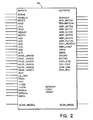
- Fig. 2 is a block diagram of a memory logic array showing the input and output signals of the array;
- Fig. 3 is a block diagram of circuitry which comprises a portion of the memory logic array of Fig. 2, the circuitry functioning in a memory array board application; and
- Fig. 4 is a block diagram of circuitry which comprises a portion of the memory logic array of Fig. 2, the circuitry functioning in a memory controller application.
- Referring now to Fig. 1 there is shown in block diagram form a portion of a digital
data processing system 10 having a preferred embodiment of the invention.System 10 can be seen to be comprised of a plurality of discrete memory units, such asmemory boards system 10 may comprise more than two memory boards. - Address and data information are provided to the memory boards via a memory bus (MEMBUS) 24 which is sourced from a memory control unit (MCU) 26.
Memory control unit 26 is coupled to a system address, control and data bus (SYSBUS) 28 and in general operates to interpret address and control information appearing on SYSBUS 28 which relates to data read/write operations to be performed upon one of thememory boards - The
system 10 also comprises asystem console 30 which may be a data processing system such as a personal computer or some other data processing system which is operable for monitoring the operation and status of thesystem 10.System console 30 typically comprises an operator output device such as a well knowndisplay monitor 32 and an operator input device such as akeyboard 34. By means of thedisplay monitor 32 andkeyboard 34 an operator is enabled to determine the status of thesystem 10 and to control various aspects of the operation thereof. - In the preferred embodiment of the invention the
system console 30 is coupled to thesystem 10 via a serial diagnostic bus (SDB) 36 which comprises a two-bit wide serial bus. The SDB 36 is preferably coupled to each of the major system units, such as thememory control unit 26, such that the system console is effectively coupled to substantially all of the major system units. - The interface between the SDB and each of the system units is accomplished by a system control interface unit (SCIU) 38. A description of the SCIU 38 will be provided hereinafter. In accordance with the invention the
system console 30 is enabled to read status information from thememory boards memory boards MCU 26. In the preferred embodiment of the invention theMLAs 40 are comprised of a highly integrated gate array semiconductor device, each of which is identical. The specific function of each of theMLAs 40, that is whether theMLAs 40 function upon one of the memory boards or upon theMCU 26, is determined by the logical state of an MCU input. For example, if the MCU input is at a logic high theMLA 40 is configured to function upon theMCU 26. Conversely, if the MCU input is a logic low theMLA 40 is configured to function upon one of thememory boards - Fig. 2 illustrates one of the
MLAs 40 and shows the input and output terminals thereof. It should be pointed out that certain of the input/output terminals are coupled toMEMBUS 24 and that internal circuitry performs memory timing, memory array selection, memory access, refresh and other functions related to the general operation of the memory devices upon the associated memory board. For theMLA 40 uponMCU 26 these memory device control related pins are generally unused. - Communication between the
MLAs 40 is accomplished by a scan bus (SCANBUS) 42 which comprises a SCANMODE signal line and bit serial SCANIN and SCANOUT signal lines. Synchronization of the internal operation of theMLAs 40 and the communication over the bit serial SCANBUS 42 is accomplished by a memory clock (MEMCLK) signal line which is coupled to each of the MLAs. In the preferred embodiment of the invention the MEMCLK signal has a period of approximately 38 nanoseconds. The MEMCLK signal is divided by four within each of the MLAs to provide the basic MLA operating clock frequency. - The direction of data flow upon the SCANBUS 41 is controlled by the logic state of the SCANMODE signal line. The logic state of SCANMODE specifies whether data is being sourced from the
MLA 40 upon theMCU 26 or whether the data is being sourced by anMLA 40 upon one of thememory boards MLA 40 upon theMCU 26 is connected in common to a SCANIN input pin of theMLAs 40 upon the memory boards. Conversely, the SCANOUT signal of each of theMLAs 40 upon the memory boards are coupled together in common and are further coupled to the SCANIN pin of theMLA 40 ofMCU 26. - Communication between MLAs is initiated by the
MLA 40 upon the MCU 26 which in turn is controlled, via SCIU 38, by thesystem console 30. - The MLA on each memory board has five registers which contain information relating to the memory board. Board ID (BDID) is a register which is serially loaded from the SCANIN pin with a memory board ID and which is compared with data which is provided, typically, but input signals lines which are hardwired to predetermined signal levels. In the preferred embodiment of the invention BDID is three bits in width such that up to eight unique board IDs may be utilized. The three bits are hardwired to logic levels on a backplane to which the memory boards are coupled.
- Board status (BDSTAT) is a register which is also serially loaded fromthe SCANIN pin and is used to indicate how much of the memory upon the memory board is to be disabled. BDSTAT is a two bit register which conveys information for enabling both MAs, disabling one or the other of the MAs, or provides for disabling both of the MAs. The contents of BDSTAT are transferred to a pair of status flip/flops only within an MLA which detects a match between BDID and its externally provided ID. This aspect of the invention will be discussed in detail below.
- Board base address (BDBA) is a register which holds the base address which a MLA provides to another MLA via base address
output signal lines 46. In the preferred embodiment of the invention, each MLA outputs six signal lines which correspond to the MSBs of the memory address bus and in general have a value which is one greater than the maximum address which the MLA responds to. This base address thereby provides to the subsequent memory board the memory address at the beginning of the memory address range to which the subsequent board will respond. It can be appreciated that since memory boards preferably represent logically contiguous, partioned sections of the physical address space of the system that if a portion of the memory upon one of the memory boards is disabled that the base address output signal lines must change state to indicate the reduction in memory capacity of the memory board. As will be described, this change of state causes other "downstream" memory boards to automatically remap their corresponding range of memory addresses such that the contiguous partioning of the memory space is preserved. The base address input signal lines of the first memory board in the system, forexample memory board 12, may be hardwired to desired logic signal levels. In the preferred embodiment of the invention these input signal lines are coupled to signal ground and thus thefirst memory board 12 responds to addresses within an address range of zero to the value determined by the setting of a plurality ofboard size jumpers 48, which will be discussed below. - Another register is board match (BDMATCH) which is a one bit register which indicates whether a memory address on
MEMBUS 24 is a memory address which is within the range of addresses which a particular memory board responds to. That is, any particular memory access which occurs uponMEMBUS 24 will result in only one of the MLAs setting the BDMATCH register, that MLA being installed upon the memory board which responds to the particular memory address. BDMATCH is set by logic which compares the six MSBs of the address bus, which are input to each MLA on pins A[2:7], to logic signals which are related to the six base address inputs and the six base address outputs, in conjunction with logic signals related to the amount of memory which is enabled upon the memory board and also to the board size. - Another register is designated board size (BDSIZE) and is typically set by the externally provided switches 48 which indicate the amount of memory installed upon the memory board. In the preferred embodiment of the invention the board size register is two bits in width and assumes values which correspond to a board size, or memory capacity, of 16, 32, 64 or 128 megabytes. The value of the BDSIZE register is used in conjunction with circuitry, which will be described below, in order to determine the value of the base
address outut signal 46. - A scan register (SCANREG) holds data received by the
MLA 40 upon theMCU 26 from theMLAs 40 on thememory boards MLA 40 ofMCU 26 and is used to indicate that SCANREG has been fully loaded from a previously specifiedMLA 40 upon a memory board. The value of MCUDR is determined by theSCIU 38, in a manner which ill be described hereinafter, in order to facilitate the transfer of data from the MLAs to thesystem console 30. - The aforementioned MCU input pin of each of the MLAs is utilized to determine the function of certain of the input lines of the MLA. When the logic state of the MCU input pin is high, the
SCIU 38 provides control and data inputs to theMLA 40 upon theMCU 26 via the same input pins which are used for the base address and the board size in anMLA 40 upon one of the memory boards. - One of these inputs is SCIU Command (SCIU CMD) which is connected to one of the base address lines of the
MLA 40 ofMCU 26 and indicates, when high, that theMLA 40 is to scan the memory board specified by SCIU ID. SCIU ID is a three bit signal connected to three of the base address input lines and specifies the board ID of one of the memory boards whoseMLA 40 is to be scanned. Alternatively, when SCIU CMD is low SCIU ID specifies pairs of bits previously stored in SCANREG which are to be read out to theSCIU 38. The selected pairs of bits are read out to theSCIU 38 upon two SCIU READ signal lines. - When the logic state of the SCIU CMD specifies that a scan operation is to be performed a two bit signal SCIU STAT is provided to the MLA upon the BDSIZE input lines for inputting the two bit status code of the memory board to be scanned. The codes have the following meaning:
00, both MAs enabled;
01, the lower MA is disabled;
10, the upper MA is disabled; and
11, both MAs are disabled. - In general, the operation of the system is as follows.
System console 30 maintains a record of the current status of each of thememory boards system console 30 determines that a hardware memory error in a specific range of addresses has occurred, such as by the occurrence of a noncorrectable double bit memory error,system console 30 scans theMLA 40 upon the memory boards to locate a memory board which includes the failing address or range of failing addresses. To accomplish this function, thesystem console 30 provides a memory board ID and a two bit code indicating the present status of that memory board viaSDB 36 to SCIU 38.SCIU 38 thereafter sets SCIU CMD to indicate that a scan operation is to occur and subsequently places the desired board ID and that boards present status code onto the signal lines SCIU ID and SCIU STAT, respectively. In response to these signals theMLA 40 upon theMCU 26 performs a scan operation. First,MLA 40 sets the SCANMODE signal to indicate that data is to flow to theMLAs 40 on the memory boards and thereafter serially outputs the contents of BDID and BDSTAT via the SCANOUT signal lines to all theMLAs 40 on the memory boards. As the contents of BDID and BDSTAT arrive at each of theMLAs 40 the MLAs serially input the ID data into their BDID registers and the status information into their BDSTAT registers. When these five bits of data have been inputted SCANMODE makes a transition from low to high, causing eachMLA 40 onmemory boards MLA 40 on the specified memory board sets the two board status flip/flops from the value of BDSTAT and also sets a flip/flop which enables theMLA 40 to drive the SCANOUT signal line. Those MLAs not detecting a match between BDID and their ID inputs reset their SCANOUT enabling flip/flop, thereby ensuring that only one MLA is enabled to drive SCANOUT during any given scan. Of course, these nonselected MLAs do not change the state of their status flip/flops. During the initial scan of each of the MLAs thesystem console 30 preferably provides the current value of BDSTAT so that no change of state occurs in the selected MLA's status flip/flops. - Subsequent to the transmission of BDID and BDSTAT, the aforementioned change of state from low to high of SCANMODE indicates that data is to flow from the selected
MLA 40 on the memory board to theMLA 40 on theMCU 26. The selectedMLA 40 upon the memory board responds to the change of state of SCANMODE by serially outputting on SCANOUT the contents of BDBA (ADRREG[0:5]), BDMATCH, BDSIZE and BDID via the SCANIN signal line to theMLA 40 onMCU 26. In addition, the selected MLA first outputs an active low signal BRDINSLOT which is indicative, when asserted, that a memory board is physically installed within the addressed slot. If BRDINSLOT is later determined to be high the other data fields can be ignored. When the registers within theMLA 40 ofMCU 26 have been loaded with this data, theMLA 40 onMCU 26 sets the MCUDR signal line to reflect the completion of the loading. - The following table summarizes the aforedescribed data transfers on a cycle by cycle basis. An "X" indicates that the data appearing on the associated pin is not relevant during the corresponding cycle.
CYCLE SCANOUT SCANMODE SCANIN MCUDR 0 SCIUID[0] 0 X 0 1 SCIUID[1] 0 X 0 2 SCIUID[2] 0 X 0 3 SCIUSTAT[0] 0 X 0 4 SCIUSTAT[1] 1 BRDINSLOT 0 5 X 1 ADRREG[0] 0 6 X 1 ADRREG[1] 0 7 X 1 ADRREG[2] 0 8 X 1 ADRREG[3] 0 9 X 1 ADRREG[4] 0 10 X 1 ADRREG[5] 0 11 X 1 BDMATCH 0 12 X 1 BDSIZE[0] 0 13 X 1 BDSIZE[1] 0 14 X 1 BDID[0] 0 15 X 1 BDID[1] 0 16 X 1 BDID[2] 0 17 X 0 X 1 -
SCIU 38 typically polls the value of MCUDR to determine when these values have been loaded and thereafter serially scans out of theMLA 40 onMCU 26, two bits at a time, the values of these registers. The data is subsequently transferred viaSDB 36 to thesystem console 30. - In general, if a memory error occurred because a memory board did not respond to a memory access, as opposed to an access which resulted in, for example, a double bit error, this occurrence will be indicated by the value of BDMATCH. That is, if an address was provided on
MEMBUS 24 which a memory board should have responded to but did not, BDMATCH being low will indicate that this response did not occur. - The following table illustrates the logical states of the SCIU ID signal lines and the corresponding data appearing on the SCIU READ data lines. SCIU CMD is assumed to be low.
SCIU ID SCIU READ[0] SCIU READ[1] 000 MCUDR BRDINSLOT 001 ADRREG[0] ADRREG[1] 010 ADRREG[2] ADRREG[3] 011 ADRREG[4] ADRREG[5] 100 BDMATCH BDSIZE[0] 101 BDSIZE[1] BDID[0] 110 BDID[1] BDID[2] 111 X X (reset MCUDR) - By sequentially scanning the memory boards coupled to
MEMBUS 24 in the above described manner, thesystem console 30 identifies, at least from BDBA and BDSIZE, which memory board and which memory array thereon includes the address or range of addresses at which the failure occurred. - Having determined which of the memory boards and which portion thereof has malfunctioned,
system console 30 thereafter again initiates a scan of the MLA 40s as previously described. However, during this subsequent scan the BDSTAT of theMLA 40 on the defective memory board is changed to disable the malfunctioning memory array(s). When theMLA 40 on the defective memory board scans in the revised status information theMLA 40 determines a new value for BDBA, thereby decreasing the value of BDBA by an amount equal to the amount of the memory which has been disabled. That is, thesystem console 30 scans theMLA 40 and sets BDSTAT as required by that memory board. TheMLAs 40 on subsequent memory boards automatically determine the address ranges for their associated memory boards in the newly reconfigured memory address space. This is accomplished by eachMLA 40 changing the state of the base address output signal lines such that an adjacent MLA in the sequential chain of MLAs determines a new value for its base address output signal. After scanning the last memory board a system address having a value greater than the highest address corresponding to installed memory will be indicated by the base address output signal lines ofMLA 40 onMCU 26. This value is preferrably utilized as an illegal address threshold value against which incoming addresses associated with a memory request are compared. - Referring now to Fig. 3 there is shown a block diagram of a portion of the circuitry within one of the MLAs; specifically that circuitry which is utilized on an
MLA 40 upon one of thememory boards 12. In Fig. 3 it can be seen that the MEMCLK input is divided by four to provide a MEMCLK/4 signal which is utilized for internal timing within the MLA. The SCANIN pin is coupled to the input of a serial data reception means, such as ashift register 50, the register being clocked with MEMCLK/4. Data sourced fromtheMLA 40 uponMCU 26 is clocked intoshift register 50 until four bits of data have been so clocked in. After transmitting the fifth bit of data the state of the SCANMODE pin is changed by theMLA 40 from a logic zero to a logic one which enables a comparison of the board ID inputs with the board ID clocked in. This comparison is accomplished by a comparison means, such as acomparator 52, which has an output a signal SCANOUT ENABLE. In addition, the two BDSTAT signals are clocked into storage means, such as status flip/flops flops ADDER logic block 56 which has outputs which are provided to an adding means, such as anADDER circuit 58. ADDERcircuit 58 also has as inputs the base address input signal lines. As previously described, these input signal lines for theMLA 40 onmemory board 12 may be a logic zero and for other MLAs are a function of the base address output signals of a previous MLA.ADDER 58 effectively adds output signals from theADDER logic block 56 to the base address input signal lines to provide the six base address output signal lines. The base address output signal lines are thus greater than the base address input signal lines by an amount equal to board size less the amount of memory which is disabled, as indicated by the status flip/flops. - The
MLA 40 also comprises an address comparison means, such as acomparator 60, which compares the address inputs A2-A7 fromMEMBUS 24 to determine if the A2-A7 address signal lines correspond to a range of addresses upon the memory board. A2-A7 are typically the MSBs of the memory address bus.Address comparator 60 has a MATCH output which is true if the A2-A7 address inputs indicate that the addressed memory location is upon the corresponding memory board. BDMATCH is the registered version of the MATCH output and is stored within a flip/flop 62. The MATCH output is utilized, in conjunction with memory enable logic 63, to initiate an access to memory devices within a given memory array as defined by the address and control signal lines which compriseMEMBUS 24. If one or both of the outputs of status flip/flops - The SCANOUT ENABLE signal being true indicates that the MLA has been addressed by the MLA upon the
MCU 26. The addressed MLA thereafter drives onto its SCANOUT signal line the values of the various internal signals as previously described. This is accomplished in part by a parallel to serial conversion means 64, which may comprise a sequential chain if flip/flops and multiplexers. - The SCANOUT signal line is connected, as previously described, to the SCANIN pin of the
MLA 40 upon theMCU 26. - Referring now to Fig. 4 there is shown circuitry operable for implementing the transmission of data from the
MLA 40 onMCU 26 to theSCIU 38. A pair ofmultiplexers MLA 40; the register outputs reflecting the data previously scanned in from a selectedMLA 40 on one of the memory boards.Multiplexers flop 74 is reset by the aforedescribed SCIU ID code 111 asserted in conjunction with SCIU CMD being low. - It should be realized that a presently preferred embodiment of the invention has been presented and that modifications to this embodiment may occur to those having skill in this art. For example, although the
MLA 40 of the presently preferred embodiment is comprised of a highly integrated gate array semiconductor device the invention may be equally well realized by a number of circuit means, including discrete integrated circuit devices such as multiplexers, flip/flops and gates. Furthermore, although the invention has been described in the context of a system console coupled by a serial diagnostic bus to a SCIU device for interfacing to theMLA 40 onMCU 26 it can be appreciated that any suitable means may be employed for interfacing to theMLA 40. For example, theMLA 40 uponMCU 26 may be directly coupled to I/O pins of a microprocessor device or to logic devices configured for inputting and receiving data from theMLA 40 in accordance with the protocol described above.
Claims (9)
for the system console:
detecting the occurrence of a memory error at an address location within the range of address locations defined by the memory units; and
outputting to the memory unit controlling means a memory unit identification code and status data expressive of one or more banks, if any, of data storage locations which are currently disabled upon the memory unit;
for the memory unit controlling means;
outputting in a simultaneous manner to each of the memory units the identification code and status data;
for each of the memory units
comparing the identification code to a predefined identification code to determine a match therebetween;
for a memory unit detecting a match
outputting to the memory unit control means a plurality of data fields expressive at least of:
the base memory address of a logically contiguous memory unit;
the number of data storage locations which comprise the memory unit; and
the identification code of the memory unit;
for the memory unit control means:
receiving the data transmitted from the identified memory unit; and
transmitting the received data to the system console;
for the system console;
receiving the data transmitted from the memory unit control means; and
determining if the address location of the memory error is within a range of addresses upon the presently identified memory unit as determined from the base address data field and from the number of storage locations data field;
if the memory error is so determined to be within the presently identified memory unit:
identifying a memory bank having the memory error; and
outputting to the memory unit control means the identified memory unit identification code and a revised status data being expressive of one or more banks of data storage locations which are to be disabled upon the identified memory unit;
for the memory unit controlling means:
outputting in a simultaneous manner to each of the memory units the identification code and the revised status data;
for each of the memory units:
comparing the identification code to the predefined identification code to determine a match therebetween; and
for a memory unit detecting a match;
storing data expressive of the revised status data whereby a memory bank having the data error is disabled.
for the memory unit storing data expressive of the revised status data:
generating a revised base memory address for a logically contiguous memory unit, the revised base memory address being decreased by an amount substantially equal to the number of data storage locations within the disabled memory bank;
outputting the revised base memory address to the logically contiguous memory unit such that the logically contiguous memory unit is enabled to generate a revised base memory address for another memory unit.
at least one memory array (16) comprising data storage means; and
a first bus (24) coupling the memory unit to the memory control unit for transferring at least memory addresses from the memory control unit to the memory array;
the memory unit further characterized by
a second bus (42) coupling the memory unit to the memory control unit, the second bus comprising:
a first bit serial signal line for transferring, when active, information from the memory control unit to the memory unit;
a second bit serial signal line for transferring, when active, information from the memory unit to the memory control unit; and
a third signal line for conveying either a first logical state for indicating that the first bit serial signal line is active or a second logical state for indicating that the second bit serial signal is active.
first means for determining a total storage capacity of the memory unit;
second means for determining a base memory address of the memory unit; and
third means, coupled to the first and the second means, for determining a base memory address of another memory unit.
Applications Claiming Priority (2)
| Application Number | Priority Date | Filing Date | Title |
|---|---|---|---|
| US179162 | 1988-04-08 | ||
| US07/179,162 US4943966A (en) | 1988-04-08 | 1988-04-08 | Memory diagnostic apparatus and method |
Publications (3)
| Publication Number | Publication Date |
|---|---|
| EP0336435A2 true EP0336435A2 (en) | 1989-10-11 |
| EP0336435A3 EP0336435A3 (en) | 1991-02-27 |
| EP0336435B1 EP0336435B1 (en) | 1995-06-14 |
Family
ID=22655479
Family Applications (1)
| Application Number | Title | Priority Date | Filing Date |
|---|---|---|---|
| EP89106176A Expired - Lifetime EP0336435B1 (en) | 1988-04-08 | 1989-04-07 | Memory diagnostic apparatus and method |
Country Status (6)
| Country | Link |
|---|---|
| US (1) | US4943966A (en) |
| EP (1) | EP0336435B1 (en) |
| JP (1) | JP2891474B2 (en) |
| AU (1) | AU615995B2 (en) |
| CA (1) | CA1315409C (en) |
| DE (1) | DE68923026T2 (en) |
Cited By (2)
| Publication number | Priority date | Publication date | Assignee | Title |
|---|---|---|---|---|
| WO1992005492A1 (en) * | 1990-09-25 | 1992-04-02 | Digital Equipment Corporation | Apparatus and methods for distributed address decoding and memory configuration |
| WO1999038075A1 (en) * | 1998-01-26 | 1999-07-29 | Memory Corporation Plc | Defect-tolerant memory system |
Families Citing this family (24)
| Publication number | Priority date | Publication date | Assignee | Title |
|---|---|---|---|---|
| US6304987B1 (en) * | 1995-06-07 | 2001-10-16 | Texas Instruments Incorporated | Integrated test circuit |
| US5317707A (en) * | 1989-10-20 | 1994-05-31 | Texas Instruments Incorporated | Expanded memory interface for supporting expanded, conventional or extended memory for communication between an application processor and an external processor |
| US5105425A (en) * | 1989-12-29 | 1992-04-14 | Westinghouse Electric Corp. | Adaptive or fault tolerant full wafer nonvolatile memory |
| US5012408A (en) * | 1990-03-15 | 1991-04-30 | Digital Equipment Corporation | Memory array addressing system for computer systems with multiple memory arrays |
| US6675333B1 (en) * | 1990-03-30 | 2004-01-06 | Texas Instruments Incorporated | Integrated circuit with serial I/O controller |
| US5166936A (en) * | 1990-07-20 | 1992-11-24 | Compaq Computer Corporation | Automatic hard disk bad sector remapping |
| JPH0498342A (en) * | 1990-08-09 | 1992-03-31 | Mitsubishi Electric Corp | Semiconductor memory device |
| US5530934A (en) * | 1991-02-02 | 1996-06-25 | Vlsi Technology, Inc. | Dynamic memory address line decoding |
| US5448710A (en) * | 1991-02-26 | 1995-09-05 | Hewlett-Packard Company | Dynamically configurable interface cards with variable memory size |
| EP0541288B1 (en) * | 1991-11-05 | 1998-07-08 | Fu-Chieh Hsu | Circuit module redundacy architecture |
| US5831467A (en) * | 1991-11-05 | 1998-11-03 | Monolithic System Technology, Inc. | Termination circuit with power-down mode for use in circuit module architecture |
| US5576554A (en) * | 1991-11-05 | 1996-11-19 | Monolithic System Technology, Inc. | Wafer-scale integrated circuit interconnect structure architecture |
| US5498990A (en) * | 1991-11-05 | 1996-03-12 | Monolithic System Technology, Inc. | Reduced CMOS-swing clamping circuit for bus lines |
| WO1994003901A1 (en) | 1992-08-10 | 1994-02-17 | Monolithic System Technology, Inc. | Fault-tolerant, high-speed bus system and bus interface for wafer-scale integration |
| US5655113A (en) | 1994-07-05 | 1997-08-05 | Monolithic System Technology, Inc. | Resynchronization circuit for a memory system and method of operating same |
| US5969538A (en) | 1996-10-31 | 1999-10-19 | Texas Instruments Incorporated | Semiconductor wafer with interconnect between dies for testing and a process of testing |
| US6219467B1 (en) * | 1997-07-15 | 2001-04-17 | Fuji Photo Film Co. Ltd. | Image processing device |
| US6405335B1 (en) | 1998-02-25 | 2002-06-11 | Texas Instruments Incorporated | Position independent testing of circuits |
| US6728915B2 (en) | 2000-01-10 | 2004-04-27 | Texas Instruments Incorporated | IC with shared scan cells selectively connected in scan path |
| US6769080B2 (en) | 2000-03-09 | 2004-07-27 | Texas Instruments Incorporated | Scan circuit low power adapter with counter |
| US6829721B2 (en) * | 2001-02-05 | 2004-12-07 | M-Systems Flash Disk Pioneers Ltd. | Method for recording and storage of system information in multi-board solid-state storage systems |
| US20060070077A1 (en) * | 2004-09-30 | 2006-03-30 | Microsoft Corporation | Providing custom product support for a software program |
| US7818625B2 (en) * | 2005-08-17 | 2010-10-19 | Microsoft Corporation | Techniques for performing memory diagnostics |
| US9946658B2 (en) * | 2013-11-22 | 2018-04-17 | Nvidia Corporation | Memory interface design having controllable internal and external interfaces for bypassing defective memory |
Citations (5)
| Publication number | Priority date | Publication date | Assignee | Title |
|---|---|---|---|---|
| US3623011A (en) * | 1969-06-25 | 1971-11-23 | Bell Telephone Labor Inc | Time-shared access to computer registers |
| US3803560A (en) * | 1973-01-03 | 1974-04-09 | Honeywell Inf Systems | Technique for detecting memory failures and to provide for automatically for reconfiguration of the memory modules of a memory system |
| EP0111053A2 (en) * | 1982-10-29 | 1984-06-20 | International Business Machines Corporation | On-chip monitor |
| EP0226791A2 (en) * | 1985-12-19 | 1987-07-01 | International Business Machines Corporation | A memory with means for allocating address space among modules |
| EP0259859A2 (en) * | 1986-09-10 | 1988-03-16 | Nec Corporation | Information processing system capable of reducing invalid memory operations by detecting an error in a main memory |
Family Cites Families (15)
| Publication number | Priority date | Publication date | Assignee | Title |
|---|---|---|---|---|
| US31318A (en) * | 1861-02-05 | hubbard | ||
| USRE31318E (en) | 1973-09-10 | 1983-07-19 | Computer Automation, Inc. | Automatic modular memory address allocation system |
| US4099234A (en) * | 1976-11-15 | 1978-07-04 | Honeywell Information Systems Inc. | Input/output processing system utilizing locked processors |
| US4334307A (en) * | 1979-12-28 | 1982-06-08 | Honeywell Information Systems Inc. | Data processing system with self testing and configuration mapping capability |
| US4435754A (en) * | 1981-06-30 | 1984-03-06 | Ampex Corporation | Method of selecting PROM data for selective mapping system |
| US4485471A (en) * | 1982-06-01 | 1984-11-27 | International Business Machines Corporation | Method of memory reconfiguration for fault tolerant memory |
| US4479214A (en) * | 1982-06-16 | 1984-10-23 | International Business Machines Corporation | System for updating error map of fault tolerant memory |
| JPS599738A (en) * | 1982-07-09 | 1984-01-19 | Mitsubishi Electric Corp | Interface system |
| US4608690A (en) * | 1982-11-26 | 1986-08-26 | Tektronix, Inc. | Detecting improper operation of a digital data processing apparatus |
| US4527251A (en) * | 1982-12-17 | 1985-07-02 | Honeywell Information Systems Inc. | Remap method and apparatus for a memory system which uses partially good memory devices |
| US4532628A (en) * | 1983-02-28 | 1985-07-30 | The Perkin-Elmer Corporation | System for periodically reading all memory locations to detect errors |
| US4566102A (en) * | 1983-04-18 | 1986-01-21 | International Business Machines Corporation | Parallel-shift error reconfiguration |
| NZ209664A (en) * | 1983-09-29 | 1987-05-29 | Tandem Computers Inc | Memory board address assignments: automatic reconfiguration |
| JPS61177556A (en) * | 1985-02-04 | 1986-08-09 | Mitsubishi Electric Corp | Memory switching circuit |
| JPH0827758B2 (en) * | 1986-05-30 | 1996-03-21 | 富士通株式会社 | Memory system |
-
1988
- 1988-04-08 US US07/179,162 patent/US4943966A/en not_active Expired - Lifetime
-
1989
- 1989-03-22 AU AU31652/89A patent/AU615995B2/en not_active Ceased
- 1989-03-31 CA CA000595332A patent/CA1315409C/en not_active Expired - Fee Related
- 1989-04-07 DE DE68923026T patent/DE68923026T2/en not_active Expired - Fee Related
- 1989-04-07 EP EP89106176A patent/EP0336435B1/en not_active Expired - Lifetime
- 1989-04-10 JP JP1090524A patent/JP2891474B2/en not_active Expired - Fee Related
Patent Citations (5)
| Publication number | Priority date | Publication date | Assignee | Title |
|---|---|---|---|---|
| US3623011A (en) * | 1969-06-25 | 1971-11-23 | Bell Telephone Labor Inc | Time-shared access to computer registers |
| US3803560A (en) * | 1973-01-03 | 1974-04-09 | Honeywell Inf Systems | Technique for detecting memory failures and to provide for automatically for reconfiguration of the memory modules of a memory system |
| EP0111053A2 (en) * | 1982-10-29 | 1984-06-20 | International Business Machines Corporation | On-chip monitor |
| EP0226791A2 (en) * | 1985-12-19 | 1987-07-01 | International Business Machines Corporation | A memory with means for allocating address space among modules |
| EP0259859A2 (en) * | 1986-09-10 | 1988-03-16 | Nec Corporation | Information processing system capable of reducing invalid memory operations by detecting an error in a main memory |
Cited By (2)
| Publication number | Priority date | Publication date | Assignee | Title |
|---|---|---|---|---|
| WO1992005492A1 (en) * | 1990-09-25 | 1992-04-02 | Digital Equipment Corporation | Apparatus and methods for distributed address decoding and memory configuration |
| WO1999038075A1 (en) * | 1998-01-26 | 1999-07-29 | Memory Corporation Plc | Defect-tolerant memory system |
Also Published As
| Publication number | Publication date |
|---|---|
| US4943966A (en) | 1990-07-24 |
| DE68923026D1 (en) | 1995-07-20 |
| EP0336435B1 (en) | 1995-06-14 |
| EP0336435A3 (en) | 1991-02-27 |
| JPH01311347A (en) | 1989-12-15 |
| CA1315409C (en) | 1993-03-30 |
| DE68923026T2 (en) | 1996-01-25 |
| JP2891474B2 (en) | 1999-05-17 |
| AU615995B2 (en) | 1991-10-17 |
| AU3165289A (en) | 1989-10-12 |
Similar Documents
| Publication | Publication Date | Title |
|---|---|---|
| EP0336435B1 (en) | Memory diagnostic apparatus and method | |
| CA1185376A (en) | Memory system with automatic memory reconfiguration | |
| US4617624A (en) | Multiple configuration memory circuit | |
| US5499346A (en) | Bus-to-bus bridge for a multiple bus information handling system that optimizes data transfers between a system bus and a peripheral bus | |
| US4468731A (en) | Identification apparatus for use in a controller to facilitate the diagnosis of faults | |
| US6560740B1 (en) | Apparatus and method for programmable built-in self-test and self-repair of embedded memory | |
| EP0614142B1 (en) | System and method for detecting and correcting memory errors | |
| US5381538A (en) | DMA controller including a FIFO register and a residual register for data buffering and having different operating modes | |
| US6523100B2 (en) | Multiple mode memory module | |
| US5666515A (en) | Information processing system having multiple modules and a memory on a bus, where any module can lock an addressable portion of the memory by sending retry signals to other modules that try to read at the locked address | |
| US5848258A (en) | Memory bank addressing scheme | |
| AU599534B2 (en) | A diagnostic system in a data processing system | |
| NZ209664A (en) | Memory board address assignments: automatic reconfiguration | |
| JPS63221445A (en) | Memory system, related erroneous detection and corrector | |
| US4400772A (en) | Method and apparatus for direct memory access in a data processing system | |
| US4333142A (en) | Self-configurable computer and memory system | |
| EP0549218B1 (en) | A memory apparatus and method for use in a data processing system | |
| US5495422A (en) | Method for combining a plurality of independently operating circuits within a single package | |
| US5838892A (en) | Method and apparatus for calculating an error detecting code block in a disk drive controller | |
| US4707833A (en) | Fault-compensating digital information transfer apparatus | |
| EP0440445B1 (en) | System memory initialization with presence detect encoding | |
| KR100429095B1 (en) | Random Access Memory in Integrated Circuits and How to Test Them | |
| EP0619546A1 (en) | Programmable memory controller and method for configuring same | |
| EP0150523A2 (en) | Data processing system with improved memory system | |
| JPH034939B2 (en) |
Legal Events
| Date | Code | Title | Description |
|---|---|---|---|
| PUAI | Public reference made under article 153(3) epc to a published international application that has entered the european phase |
Free format text: ORIGINAL CODE: 0009012 |
|
| AK | Designated contracting states |
Kind code of ref document: A2 Designated state(s): BE DE FR GB NL |
|
| PUAL | Search report despatched |
Free format text: ORIGINAL CODE: 0009013 |
|
| AK | Designated contracting states |
Kind code of ref document: A3 Designated state(s): BE DE FR GB NL |
|
| 17P | Request for examination filed |
Effective date: 19910827 |
|
| 17Q | First examination report despatched |
Effective date: 19931104 |
|
| GRAA | (expected) grant |
Free format text: ORIGINAL CODE: 0009210 |
|
| AK | Designated contracting states |
Kind code of ref document: B1 Designated state(s): BE DE FR GB NL |
|
| REF | Corresponds to: |
Ref document number: 68923026 Country of ref document: DE Date of ref document: 19950720 |
|
| ET | Fr: translation filed | ||
| PGFP | Annual fee paid to national office [announced via postgrant information from national office to epo] |
Ref country code: NL Payment date: 19960318 Year of fee payment: 8 |
|
| PGFP | Annual fee paid to national office [announced via postgrant information from national office to epo] |
Ref country code: BE Payment date: 19960325 Year of fee payment: 8 |
|
| PLBE | No opposition filed within time limit |
Free format text: ORIGINAL CODE: 0009261 |
|
| STAA | Information on the status of an ep patent application or granted ep patent |
Free format text: STATUS: NO OPPOSITION FILED WITHIN TIME LIMIT |
|
| 26N | No opposition filed | ||
| PG25 | Lapsed in a contracting state [announced via postgrant information from national office to epo] |
Ref country code: BE Effective date: 19970430 |
|
| BERE | Be: lapsed |
Owner name: WANG LABORATORIES INC. Effective date: 19970430 |
|
| PG25 | Lapsed in a contracting state [announced via postgrant information from national office to epo] |
Ref country code: NL Effective date: 19971101 |
|
| NLV4 | Nl: lapsed or anulled due to non-payment of the annual fee |
Effective date: 19971101 |
|
| REG | Reference to a national code |
Ref country code: FR Ref legal event code: TP |
|
| REG | Reference to a national code |
Ref country code: FR Ref legal event code: TP Free format text: CORRECTION |
|
| REG | Reference to a national code |
Ref country code: GB Ref legal event code: 732E |
|
| PGFP | Annual fee paid to national office [announced via postgrant information from national office to epo] |
Ref country code: FR Payment date: 20000317 Year of fee payment: 12 |
|
| PGFP | Annual fee paid to national office [announced via postgrant information from national office to epo] |
Ref country code: DE Payment date: 20000320 Year of fee payment: 12 |
|
| PG25 | Lapsed in a contracting state [announced via postgrant information from national office to epo] |
Ref country code: FR Free format text: THE PATENT HAS BEEN ANNULLED BY A DECISION OF A NATIONAL AUTHORITY Effective date: 20010430 |
|
| REG | Reference to a national code |
Ref country code: GB Ref legal event code: IF02 |
|
| PG25 | Lapsed in a contracting state [announced via postgrant information from national office to epo] |
Ref country code: DE Free format text: LAPSE BECAUSE OF NON-PAYMENT OF DUE FEES Effective date: 20020201 |
|
| REG | Reference to a national code |
Ref country code: FR Ref legal event code: ST |
|
| PGFP | Annual fee paid to national office [announced via postgrant information from national office to epo] |
Ref country code: GB Payment date: 20080409 Year of fee payment: 20 |
|
| REG | Reference to a national code |
Ref country code: GB Ref legal event code: PE20 Expiry date: 20090406 |
|
| PG25 | Lapsed in a contracting state [announced via postgrant information from national office to epo] |
Ref country code: GB Free format text: LAPSE BECAUSE OF EXPIRATION OF PROTECTION Effective date: 20090406 |