EP0341002B1 - Thin film structure having magnetic and colour shifting properties - Google Patents
Thin film structure having magnetic and colour shifting properties Download PDFInfo
- Publication number
- EP0341002B1 EP0341002B1 EP89304351A EP89304351A EP0341002B1 EP 0341002 B1 EP0341002 B1 EP 0341002B1 EP 89304351 A EP89304351 A EP 89304351A EP 89304351 A EP89304351 A EP 89304351A EP 0341002 B1 EP0341002 B1 EP 0341002B1
- Authority
- EP
- European Patent Office
- Prior art keywords
- interference coating
- multilayer interference
- magnetic
- layer
- metallic layer
- Prior art date
- Legal status (The legal status is an assumption and is not a legal conclusion. Google has not performed a legal analysis and makes no representation as to the accuracy of the status listed.)
- Expired - Lifetime
Links
Images
Classifications
-
- G—PHYSICS
- G02—OPTICS
- G02B—OPTICAL ELEMENTS, SYSTEMS OR APPARATUS
- G02B5/00—Optical elements other than lenses
- G02B5/20—Filters
- G02B5/28—Interference filters
- G02B5/285—Interference filters comprising deposited thin solid films
-
- C—CHEMISTRY; METALLURGY
- C09—DYES; PAINTS; POLISHES; NATURAL RESINS; ADHESIVES; COMPOSITIONS NOT OTHERWISE PROVIDED FOR; APPLICATIONS OF MATERIALS NOT OTHERWISE PROVIDED FOR
- C09C—TREATMENT OF INORGANIC MATERIALS, OTHER THAN FIBROUS FILLERS, TO ENHANCE THEIR PIGMENTING OR FILLING PROPERTIES ; PREPARATION OF CARBON BLACK ; PREPARATION OF INORGANIC MATERIALS WHICH ARE NO SINGLE CHEMICAL COMPOUNDS AND WHICH ARE MAINLY USED AS PIGMENTS OR FILLERS
- C09C1/00—Treatment of specific inorganic materials other than fibrous fillers; Preparation of carbon black
- C09C1/0015—Pigments exhibiting interference colours, e.g. transparent platelets of appropriate thinness or flaky substrates, e.g. mica, bearing appropriate thin transparent coatings
-
- G—PHYSICS
- G06—COMPUTING; CALCULATING OR COUNTING
- G06K—GRAPHICAL DATA READING; PRESENTATION OF DATA; RECORD CARRIERS; HANDLING RECORD CARRIERS
- G06K19/00—Record carriers for use with machines and with at least a part designed to carry digital markings
- G06K19/06—Record carriers for use with machines and with at least a part designed to carry digital markings characterised by the kind of the digital marking, e.g. shape, nature, code
- G06K19/08—Record carriers for use with machines and with at least a part designed to carry digital markings characterised by the kind of the digital marking, e.g. shape, nature, code using markings of different kinds or more than one marking of the same kind in the same record carrier, e.g. one marking being sensed by optical and the other by magnetic means
- G06K19/10—Record carriers for use with machines and with at least a part designed to carry digital markings characterised by the kind of the digital marking, e.g. shape, nature, code using markings of different kinds or more than one marking of the same kind in the same record carrier, e.g. one marking being sensed by optical and the other by magnetic means at least one kind of marking being used for authentication, e.g. of credit or identity cards
-
- G—PHYSICS
- G11—INFORMATION STORAGE
- G11B—INFORMATION STORAGE BASED ON RELATIVE MOVEMENT BETWEEN RECORD CARRIER AND TRANSDUCER
- G11B7/00—Recording or reproducing by optical means, e.g. recording using a thermal beam of optical radiation by modifying optical properties or the physical structure, reproducing using an optical beam at lower power by sensing optical properties; Record carriers therefor
- G11B7/24—Record carriers characterised by shape, structure or physical properties, or by the selection of the material
-
- C—CHEMISTRY; METALLURGY
- C01—INORGANIC CHEMISTRY
- C01P—INDEXING SCHEME RELATING TO STRUCTURAL AND PHYSICAL ASPECTS OF SOLID INORGANIC COMPOUNDS
- C01P2006/00—Physical properties of inorganic compounds
- C01P2006/42—Magnetic properties
-
- Y—GENERAL TAGGING OF NEW TECHNOLOGICAL DEVELOPMENTS; GENERAL TAGGING OF CROSS-SECTIONAL TECHNOLOGIES SPANNING OVER SEVERAL SECTIONS OF THE IPC; TECHNICAL SUBJECTS COVERED BY FORMER USPC CROSS-REFERENCE ART COLLECTIONS [XRACs] AND DIGESTS
- Y10—TECHNICAL SUBJECTS COVERED BY FORMER USPC
- Y10S—TECHNICAL SUBJECTS COVERED BY FORMER USPC CROSS-REFERENCE ART COLLECTIONS [XRACs] AND DIGESTS
- Y10S283/00—Printed matter
- Y10S283/902—Anti-photocopy
Definitions
- This invention relates to a thin film structure having magnetic and optically variable characteristics and more particularly to a magnetic optically variable pigment and device.
- EP-A-170832 discloses a thin film structure in which a magnetic layer is embossed into a diffraction grating structure.
- Another object of the invention is to provide a pigment and device of the above character which can be readily manufactured.
- This invention provides a thin film structure having optically variable properties providing substantial colour shift with angle of incidence and viewing comprising a substrate and a multilayer thin film metal-dielectric interference coating including a reflective metallic layer carried by the substrate to produce said inherent colour shift with angle; wherein in that said metallic layer is formed of a material which has magnetic as well as reflective properties, said metallic layer forming an integral part of the multilayer thin film metal-dielectric interference coating to contribute to the optically variable properties to provide one anticounterfeiting feature, said same metallic layer also contributing to the magnetic properties to provide another anticounterfeiting feature.
- the thin film structure having magnetic and optically variable properties consists of a multilayer interference coating which produces an inherent color shift with angle.
- the interference coating has a metal-dielectric design.
- the metal utilized in the design has magnetic properties to permit recording of information magnetically in the metal.
- a subtractive colored superstrate is provided external of the multilayer interference coating on the side of the multilayer interference coating facing the incident light.
- the colored superstrate also called a subtractive colorant means
- This combination of a subtractive colorant means and the multilayer interference coating provides a discrete color shift from one distinct color to another at two different angles of incidence, and/or modifies the colors produced by the interference coating.
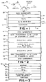
- a thin film structure is in the form of a magnetic color shifting optically variable device 11.
- a substrate 12 which can be formed of a suitable material such as PET or other suitable material as set forth in U.S. Patent No. 4,705,356.
- the substrate 12 is provided with first and second surfaces 13 and 14.
- a multilayer interference coating 16 is provided on the first surface 13.
- the multilayer interference coating 16 has a metal-dielectric design which consists of a periodic structure of alternating metal and dielectric layers on a relatively high reflecting opaque metal layer 17.
- the metal dielectric design in its simplest form can be a three layer combination such as shown in Figure 1.
- the first metal layer 17 is preferably a highly reflecting metal layer.
- the metal is chosen so that in addition to having high reflecting properties it also has magnetic qualities for a purpose hereinafter described.
- One metal found to be particularly suitable for this application is a cobalt nickel alloy with a ratio by weight of 80% cobalt and 20% nickel plus or minus 10% for each metal. Such a metal layer is deposited on the surface 13 to a thickness so that it is substantially opaque.
- An optical spacer layer 18 in the form of a suitable dielectric (i.e., having a low index of refraction) such as magnesium fluoride is deposited on the cobalt nickel layer 17.
- a metal with high absorption properties is then deposited on the dielectric layer 18 to provide an absorber layer 19.
- One metal found to be suitable for this is chromium.
- Other metals which have such high absorption characteristics can be selected in the manner suggested in U.S. Patent No. 4,705,356.
- the basic reflectance profile for the three-layer metal-dielectric design for the interference filter 16 would be essentially retained in designs employing additional periods of the thin metal and dielectric.
- the multilayer interference coating 16 provide an inherent color shift with the change in viewing angle.
- the incident light is indicated by ray 21a or ray 21 b and the reflected light is indicated by ray 22a or 22b as viewed by the eye 23a or 23b.
- the eye position of 23a one sees one color, Color A, and at position 23b another color, Color B.
- subtractive colorant means is provided external of the multilayer interference coating on the side of the multilayer interference coating 16 facing the incident light.
- This subtractive colorant means in combination with a multilayer interference coating serves to modify the inherent color shift produced by the multilayer interference coating to provide a discrete color shift from one distinct color to another distinct color at two different angles of incidence.
- This subtractive colorant means can take the form of a dyed superstrate 26 as shown in Figure 1.
- the dyed superstrate 26 must be optically thickand have a minimum thickness in the range of about 1.5 to 2.0 microns.
- the optical variable device or structure shown in Figure 1 can be utilized in the manner described in U.S. Patent No. 4,705,356. In addition, it can be utilized to encode information in the magnetic layer 17. For example, it could record the typical information which is carried by a credit card in a magnetic stripe. It also could be utilized for putting the numbers on the bottoms of checks so that the information carried by the check could be read magnetically as with present day checks and still provide the optical variable feature.
- the present invention can be incorporated in a magnetic and optically variable ink by providing flakes in the manner described in EP - A- 0227423.
- the absorber layer also could be formed of the cobalt nickel alloy. This simplifies the manufacture of the magnetic optically variable device or structure by only using a single metal and a single dielectric.
- FIG. 2 Another embodiment of the thin film structure having magnetic and optical variable properties is shown in Figure 2 and takes the form of a magnetic optically variable pigment.
- this pigment is comprised of a symmetrical design which lends itself to being broken up into flakes which can be utilized in making pigment in the manner described in EP - A - 0227423.
- the symmetrical design 31 shown in Figure 2 is formed using a reflecting metallic layer which also has magnetic properties.
- the metal is selected for its reflecting properties as well as its magnetic properties.
- the metal is deposited to a thickness so that it is substantially opaque.
- One metal found to be satisfactory is a cobalt nickel alloy with the cobalt nickel having a ratio by weight of 80% and 20% respectively.
- the reflecting layer 32 is provided with first and second reflecting surfaces 33 and 34.
- Dielectric spacer layers 36 and 37 are provided on the surfaces 33 and 34 and are formed of a suitable low index of refraction material such as magnesium fluoride.
- Metallic absorber layers 38 and 39 formed of a suitable absorber metal such as chromium are deposited on the dielectric layers 36 and 37. They are deposited to a thickness so that they are semi-transparent. As pointed out previously, when it is desired to use only a single metal in the structure, the chromium layer can be replaced with the cobalt nickel alloy utilized for the reflecting layer 32.
- dyed superstrates 41 and 42 are provided on the metal layers 38 and 39 to provide subtractant colorant means of the type hereinbefore described in connection with Figure 1.
- FIG. 2 The structure which is shown in Figure 2 can be prepared in flake form in the manner described in EP - A - 0227423.
- the symmetrical design particularly lends itself to such an application.
- a magnetic optically variable pigment can be provided in which magnetic information can be encoded in the paint incorporating the pigment or in which the pigment simply exhibits magnetic properties so that it can be utilized in credit cards, checks and the like in the manner hereinbefore described.
- FIG. 3 An alternate construction of a device incorporating the present invention is shown in Figure 3 which is transferrable and generally comprises a metal dielectric thin film stack which can be provided with or without a subtractive colorant placed on a releasable hardcoat substrate which can be transferred to another substrate.
- This device 46 as shown in Figure 3 consists of a transparent flexible substrate formed of a suitable material such as PET.
- the substrate 47 is provided with surfaces 48 and 49.
- a releasable hardcoat or releasable layer 51 is deposited on the surface 48 and is of a conventional type.
- the release layer 51 can be formed of any suitable material such as a wax, silicone or acrylic and can have a suitable thickness such as approximately 1 micron.
- the releasable material should be one which can be carry a color so that a dyed releasable hardcoat can be provided when that effect is desired.
- the release layer When the release layer is dyed it provides the subtractive colorant means in the dyed superstrates in the previous embodiments of the present invention.
- a metallic layer 52 is deposited on the release layer 51 and is formed of a suitable material such as chromium. This metallic layer serves as one of the metal layers in the metal dielectric stack.
- the dielectric is formed by a layer 53 formed of a suitable dielectric having a low index of refraction as, for example, magnesium fluoride.
- Another metal layer 54 formed of a cobalt nickel composition of the type hereinbefore described as, for example, an 80-20% by weight mixture is disposed on the dielectric layer 53.
- An adhesive layer 56 is deposited on the metal layer 54.
- the adhesive can be a conventional hot stamp adhesive or other suitable type of adhesive such as a pressure sensitive adhesive.
- the adhesive layer 56 can have a suitable thickness such as approximately 1/2 mil (12.7 pm).
- the metal dielectric stack which is shown in Figure 3 can be readily transferred to another article.
- a hot die stamp can be utilized to stamp out the desired image and to heat the adhesive so that the adhesive will adhere to the transfer substrate at the places where it is heated.
- the device of the present invention will only be transfered in the areas where heat has been applied.
- the structure or device can be placed in a bar code pattern which would produce an optically variable bar code device that would appear on a label or on the article itself.
- a bar code would function as an optically variable bar code that could be read by both optical and magnetic readers.
- Such a bar code optically variable device would provide three security features, the bar code itself, the optically variable characteristic and the magnetic characteristic.
Abstract
Description
- This invention relates to a thin film structure having magnetic and optically variable characteristics and more particularly to a magnetic optically variable pigment and device.
- Optical variable articles having substantial color shift with angle have been disclosed in US-A-4,705,356 and US-A-4,705,300. However, it has been found when such an article is utilized in security applications as well as in anticounterfeit applications there is a need for additional security. This is true in both pigment and device applications.
- EP-A-170832 discloses a thin film structure in which a magnetic layer is embossed into a diffraction grating structure.
- In general, it is an object of the present invention to provide a thin film structure having both magnetic and optically variable characteristics.
- Another object of the invention is to provide a pigment and device of the above character which can be readily manufactured.
- This invention provides a thin film structure having optically variable properties providing substantial colour shift with angle of incidence and viewing comprising a substrate and a multilayer thin film metal-dielectric interference coating including a reflective metallic layer carried by the substrate to produce said inherent colour shift with angle; wherein in that said metallic layer is formed of a material which has magnetic as well as reflective properties, said metallic layer forming an integral part of the multilayer thin film metal-dielectric interference coating to contribute to the optically variable properties to provide one anticounterfeiting feature, said same metallic layer also contributing to the magnetic properties to provide another anticounterfeiting feature.
- The following is a description of a number of preferred embodiments of the invention which are set forth in detail in conjunction with the following drawings:
- Figure 1 is a cross sectional view of a magnetic color shifting optical variable device incorporating the present invention.
- Figure 2 is a cross sectional view of a magnetically optically variable pigment incorporating the present invention.
- Figure 3 is a cross sectional view of a device incorporating the present invention which is transferable.
- In general, the thin film structure having magnetic and optically variable properties consists of a multilayer interference coating which produces an inherent color shift with angle. The interference coating has a metal-dielectric design. The metal utilized in the design has magnetic properties to permit recording of information magnetically in the metal. When it is desired to produce a specific color shift in reflection from one color to another by removing certain colors, or to modify the color shift properties, a subtractive colored superstrate is provided external of the multilayer interference coating on the side of the multilayer interference coating facing the incident light. The colored superstrate (also called a subtractive colorant means) in combination with a multilayer interference coating serves to modify the inherent color shift produced by the multilayer interference coating. This combination of a subtractive colorant means and the multilayer interference coating provides a discrete color shift from one distinct color to another at two different angles of incidence, and/or modifies the colors produced by the interference coating.
- More particularly, as shown in Figure 1, a thin film structure is in the form of a magnetic color shifting optically variable device 11. As shown therein, it consists of a
substrate 12 which can be formed of a suitable material such as PET or other suitable material as set forth in U.S. Patent No. 4,705,356. Thesubstrate 12 is provided with first andsecond surfaces multilayer interference coating 16 is provided on thefirst surface 13. As described in U.S. Patent No. 4,705,356, themultilayer interference coating 16 has a metal-dielectric design which consists of a periodic structure of alternating metal and dielectric layers on a relatively high reflectingopaque metal layer 17. - As explained in U.S. Patent No. 4,705,356, the metal dielectric design in its simplest form can be a three layer combination such as shown in Figure 1. In such a design, the
first metal layer 17 is preferably a highly reflecting metal layer. In accordance with the present invention rather than using a highly reflective non-magnetic metal layer such as aluminum, the metal is chosen so that in addition to having high reflecting properties it also has magnetic qualities for a purpose hereinafter described. One metal found to be particularly suitable for this application is a cobalt nickel alloy with a ratio by weight of 80% cobalt and 20% nickel plus or minus 10% for each metal. Such a metal layer is deposited on thesurface 13 to a thickness so that it is substantially opaque. Anoptical spacer layer 18 in the form of a suitable dielectric (i.e., having a low index of refraction) such as magnesium fluoride is deposited on thecobalt nickel layer 17. A metal with high absorption properties is then deposited on thedielectric layer 18 to provide anabsorber layer 19. One metal found to be suitable for this is chromium. Other metals which have such high absorption characteristics can be selected in the manner suggested in U.S. Patent No. 4,705,356. - It should be appreciated that the basic reflectance profile for the three-layer metal-dielectric design for the
interference filter 16 would be essentially retained in designs employing additional periods of the thin metal and dielectric. Themultilayer interference coating 16 provide an inherent color shift with the change in viewing angle. In Figure 1, the incident light is indicated by ray 21a orray 21 b and the reflected light is indicated byray 22a or 22b as viewed by theeye 23a or 23b. At the eye position of 23a one sees one color, Color A, and atposition 23b another color, Color B. - When it is desired to produce a specific color shift or to eliminate certain colors, subtractive colorant means is provided external of the multilayer interference coating on the side of the
multilayer interference coating 16 facing the incident light. This subtractive colorant means in combination with a multilayer interference coating serves to modify the inherent color shift produced by the multilayer interference coating to provide a discrete color shift from one distinct color to another distinct color at two different angles of incidence. This subtractive colorant means can take the form of adyed superstrate 26 as shown in Figure 1. Thedyed superstrate 26 must be optically thickand have a minimum thickness in the range of about 1.5 to 2.0 microns. - The optical variable device or structure shown in Figure 1 can be utilized in the manner described in U.S. Patent No. 4,705,356. In addition, it can be utilized to encode information in the
magnetic layer 17. For example, it could record the typical information which is carried by a credit card in a magnetic stripe. It also could be utilized for putting the numbers on the bottoms of checks so that the information carried by the check could be read magnetically as with present day checks and still provide the optical variable feature. - It also should be appreciated that the present invention can be incorporated in a magnetic and optically variable ink by providing flakes in the manner described in EP - A- 0227423.
- It should be appreciated that if desired in place of the chromium absorber layer, the absorber layer also could be formed of the cobalt nickel alloy. This simplifies the manufacture of the magnetic optically variable device or structure by only using a single metal and a single dielectric.
- Another embodiment of the thin film structure having magnetic and optical variable properties is shown in Figure 2 and takes the form of a magnetic optically variable pigment. As shown in Figure 2, this pigment is comprised of a symmetrical design which lends itself to being broken up into flakes which can be utilized in making pigment in the manner described in EP - A - 0227423. The symmetrical design 31 shown in Figure 2 is formed using a reflecting metallic layer which also has magnetic properties. As explained in connection with the previous embodiment, the metal is selected for its reflecting properties as well as its magnetic properties. The metal is deposited to a thickness so that it is substantially opaque. One metal found to be satisfactory is a cobalt nickel alloy with the cobalt nickel having a ratio by weight of 80% and 20% respectively. This ratio for each of the metals can be varied by plus or minus 10% and still achieve the desired results. The reflecting layer 32 is provided with first and second reflecting
surfaces Dielectric spacer layers surfaces Metallic absorber layers dielectric layers - If a specific color shift is desired or if it is desired to remove certain colors, dyed
superstrates metal layers - The structure which is shown in Figure 2 can be prepared in flake form in the manner described in EP - A - 0227423. The symmetrical design particularly lends itself to such an application. In utilizing flakes formed from the structure shown in Figure 2, a magnetic optically variable pigment can be provided in which magnetic information can be encoded in the paint incorporating the pigment or in which the pigment simply exhibits magnetic properties so that it can be utilized in credit cards, checks and the like in the manner hereinbefore described.
- An alternate construction of a device incorporating the present invention is shown in Figure 3 which is transferrable and generally comprises a metal dielectric thin film stack which can be provided with or without a subtractive colorant placed on a releasable hardcoat substrate which can be transferred to another substrate. This
device 46 as shown in Figure 3 consists of a transparent flexible substrate formed of a suitable material such as PET. Thesubstrate 47 is provided withsurfaces releasable layer 51 is deposited on thesurface 48 and is of a conventional type. Therelease layer 51 can be formed of any suitable material such as a wax, silicone or acrylic and can have a suitable thickness such as approximately 1 micron. If desired, the releasable material should be one which can be carry a color so that a dyed releasable hardcoat can be provided when that effect is desired. When the release layer is dyed it provides the subtractive colorant means in the dyed superstrates in the previous embodiments of the present invention. - A
metallic layer 52 is deposited on therelease layer 51 and is formed of a suitable material such as chromium. This metallic layer serves as one of the metal layers in the metal dielectric stack. The dielectric is formed by alayer 53 formed of a suitable dielectric having a low index of refraction as, for example, magnesium fluoride. Anothermetal layer 54 formed of a cobalt nickel composition of the type hereinbefore described as, for example, an 80-20% by weight mixture is disposed on thedielectric layer 53. Anadhesive layer 56 is deposited on themetal layer 54. The adhesive can be a conventional hot stamp adhesive or other suitable type of adhesive such as a pressure sensitive adhesive. Theadhesive layer 56 can have a suitable thickness such as approximately 1/2 mil (12.7 pm). The metal dielectric stack which is shown in Figure 3 can be readily transferred to another article. - When it is desired to make a transfer, a hot die stamp can be utilized to stamp out the desired image and to heat the adhesive so that the adhesive will adhere to the transfer substrate at the places where it is heated. Thus the device of the present invention will only be transfered in the areas where heat has been applied.
- It should be appreciated that with a device such as shown in Figure 3, it is possible to place the adhesive on the counter surface in predetermined locations. A roll-on transfer can then be utilized which will cause the device to stick where the adhesive is present and not to stick where the adhesive is not present so that a pattern can be provided if the device is provided on the counter surface.
- It should be appreciated that in accordance with the present invention, the structure or device can be placed in a bar code pattern which would produce an optically variable bar code device that would appear on a label or on the article itself. Such a bar code would function as an optically variable bar code that could be read by both optical and magnetic readers. Such a bar code optically variable device would provide three security features, the bar code itself, the optically variable characteristic and the magnetic characteristic.
- From the foregoing it can be seen that there has been provided a thin film structure which has both magnetic and optically variable properties which lend itself to many different types of applications, particularly where additional security is desired.
Claims (11)
Applications Claiming Priority (2)
| Application Number | Priority Date | Filing Date | Title |
|---|---|---|---|
| US07/189,779 US4838648A (en) | 1988-05-03 | 1988-05-03 | Thin film structure having magnetic and color shifting properties |
| US189779 | 1988-05-03 |
Publications (4)
| Publication Number | Publication Date |
|---|---|
| EP0341002A2 EP0341002A2 (en) | 1989-11-08 |
| EP0341002A3 EP0341002A3 (en) | 1990-08-01 |
| EP0341002B1 true EP0341002B1 (en) | 1995-06-14 |
| EP0341002B2 EP0341002B2 (en) | 1999-02-24 |
Family
ID=22698739
Family Applications (1)
| Application Number | Title | Priority Date | Filing Date |
|---|---|---|---|
| EP89304351A Expired - Lifetime EP0341002B2 (en) | 1988-05-03 | 1989-04-28 | Thin film structure having magnetic and colour shifting properties |
Country Status (9)
| Country | Link |
|---|---|
| US (1) | US4838648A (en) |
| EP (1) | EP0341002B2 (en) |
| JP (1) | JP2960434B2 (en) |
| AT (1) | ATE123888T1 (en) |
| CA (1) | CA1319052C (en) |
| DE (1) | DE68923036T3 (en) |
| ES (1) | ES2072901T5 (en) |
| GR (2) | GR3017135T3 (en) |
| HK (1) | HK1005756A1 (en) |
Cited By (8)
| Publication number | Priority date | Publication date | Assignee | Title |
|---|---|---|---|---|
| WO2003059644A1 (en) | 2002-01-18 | 2003-07-24 | Giesecke & Devrient Gmbh | Security element with flip-flop color change effect and magnetic properties, article comprising such a security element and method for producing said security element and said article |
| WO2003068525A1 (en) | 2002-02-14 | 2003-08-21 | Giesecke & Devrient Gmbh | Security element and security document with one such security element |
| WO2003070482A1 (en) | 2002-02-22 | 2003-08-28 | Giesecke & Devrient Gmbh | Security document and security element for a security document |
| US7645510B2 (en) | 2002-09-13 | 2010-01-12 | Jds Uniphase Corporation | Provision of frames or borders around opaque flakes for covert security applications |
| US7670641B2 (en) | 2002-04-29 | 2010-03-02 | Cardinal Cg Company | Coatings having low emissivity and low solar reflectance |
| US7687149B2 (en) | 2002-05-16 | 2010-03-30 | Cardinal Cg Company | High shading performance coatings |
| US9027479B2 (en) | 2002-07-15 | 2015-05-12 | Jds Uniphase Corporation | Method and apparatus for orienting magnetic flakes |
| RU2568708C2 (en) * | 2014-03-18 | 2015-11-20 | Федеральное Государственное Унитарное Предприятие "Гознак" (Фгуп "Гознак") | Multi-layer polymeric protective element |
Families Citing this family (210)
| Publication number | Priority date | Publication date | Assignee | Title |
|---|---|---|---|---|
| JPH0437805A (en) * | 1990-06-04 | 1992-02-07 | Aisin Seiki Co Ltd | Reflecting mirror consisting of laminated thin film |
| CA2048564C (en) * | 1990-08-16 | 2001-10-23 | Paul Graham Coombs | Optically variable interference device with peak suppression and method |
| US5214530A (en) * | 1990-08-16 | 1993-05-25 | Flex Products, Inc. | Optically variable interference device with peak suppression and method |
| EP0549024B1 (en) * | 1991-12-12 | 1997-11-19 | Koninklijke Philips Electronics N.V. | Optical record carrier |
| US20040241454A1 (en) * | 1993-10-04 | 2004-12-02 | Shaw David G. | Barrier sheet and method of making same |
| US5510163A (en) * | 1994-05-18 | 1996-04-23 | National Research Council Of Canada | Optical storage media having visible logos |
| US5498781A (en) | 1994-05-23 | 1996-03-12 | Basf Corporation | Passification of optically variable pigment and waterborne coating compositions containg the same |
| US5513040B1 (en) * | 1994-11-01 | 1998-02-03 | Deposition Technology Inc | Optical device having low visual light transmission and low visual light reflection |
| US6235105B1 (en) | 1994-12-06 | 2001-05-22 | General Atomics | Thin film pigmented optical coating compositions |
| US5527848A (en) | 1994-12-14 | 1996-06-18 | Basf Corporation | Pacification of optically variable pigments for use in waterborne coating compositions |
| US5877895A (en) | 1995-03-20 | 1999-03-02 | Catalina Coatings, Inc. | Multicolor interference coating |
| WO1997047693A1 (en) | 1996-06-10 | 1997-12-18 | Nittetsu Mining Co., Ltd. | Multilayer coated powder |
| CN1052994C (en) * | 1996-10-04 | 2000-05-31 | 中国科学院上海技术物理研究所 | Prepn of allochronic ink capable of resulting in high productivity |
| US6262830B1 (en) | 1997-09-16 | 2001-07-17 | Michael Scalora | Transparent metallo-dielectric photonic band gap structure |
| US5907427A (en) | 1997-10-24 | 1999-05-25 | Time Domain Corporation | Photonic band gap device and method using a periodicity defect region to increase photonic signal delay |
| IT1296098B1 (en) * | 1997-11-11 | 1999-06-09 | Mantegazza Walter | SAFETY THREAD WITH OPTICAL AND MAGNETIC INFORMATION INSERTABLE IN DOCUMENTS IN GENERAL |
| US6013370A (en) * | 1998-01-09 | 2000-01-11 | Flex Products, Inc. | Bright metal flake |
| IL122928A (en) * | 1998-01-13 | 2000-10-31 | Nickel Rainbow Ltd | Articles having a colored metallic coating with special properties |
| US6304366B1 (en) | 1998-04-02 | 2001-10-16 | Michael Scalora | Photonic signal frequency conversion using a photonic band gap structure |
| US6744552B2 (en) * | 1998-04-02 | 2004-06-01 | Michael Scalora | Photonic signal frequency up and down-conversion using a photonic band gap structure |
| US6156325A (en) * | 1998-09-16 | 2000-12-05 | L'oreal | Nail enamel composition containing a urea-modified thixotropic agent |
| US6157489A (en) * | 1998-11-24 | 2000-12-05 | Flex Products, Inc. | Color shifting thin film pigments |
| US6150022A (en) | 1998-12-07 | 2000-11-21 | Flex Products, Inc. | Bright metal flake based pigments |
| US6396617B1 (en) | 1999-05-17 | 2002-05-28 | Michael Scalora | Photonic band gap device and method using a periodicity defect region doped with a gain medium to increase photonic signal delay |
| US20070195392A1 (en) * | 1999-07-08 | 2007-08-23 | Jds Uniphase Corporation | Adhesive Chromagram And Method Of Forming Thereof |
| US7604855B2 (en) | 2002-07-15 | 2009-10-20 | Jds Uniphase Corporation | Kinematic images formed by orienting alignable flakes |
| US6987590B2 (en) * | 2003-09-18 | 2006-01-17 | Jds Uniphase Corporation | Patterned reflective optical structures |
| US6761959B1 (en) * | 1999-07-08 | 2004-07-13 | Flex Products, Inc. | Diffractive surfaces with color shifting backgrounds |
| US7517578B2 (en) | 2002-07-15 | 2009-04-14 | Jds Uniphase Corporation | Method and apparatus for orienting magnetic flakes |
| US7667895B2 (en) * | 1999-07-08 | 2010-02-23 | Jds Uniphase Corporation | Patterned structures with optically variable effects |
| WO2001023948A1 (en) | 1999-09-30 | 2001-04-05 | Aguanno Giuseppe D | Efficient non-linear phase shifting using a photonic band gap structure |
| US6545809B1 (en) | 1999-10-20 | 2003-04-08 | Flex Products, Inc. | Color shifting carbon-containing interference pigments |
| US6486499B1 (en) * | 1999-12-22 | 2002-11-26 | Lumileds Lighting U.S., Llc | III-nitride light-emitting device with increased light generating capability |
| US6414780B1 (en) | 1999-12-23 | 2002-07-02 | D'aguanno Giuseppe | Photonic signal reflectivity and transmissivity control using a photonic band gap structure |
| US6339493B1 (en) | 1999-12-23 | 2002-01-15 | Michael Scalora | Apparatus and method for controlling optics propagation based on a transparent metal stack |
| CN1666888B (en) * | 2000-01-21 | 2011-12-14 | 光学涂层实验公司 | Optically variable security devices |
| US11768321B2 (en) | 2000-01-21 | 2023-09-26 | Viavi Solutions Inc. | Optically variable security devices |
| US6515787B1 (en) | 2000-03-07 | 2003-02-04 | Eclipse Energy Systems, Inc. | Electrochromic layer |
| US7152047B1 (en) | 2000-05-24 | 2006-12-19 | Esecure.Biz, Inc. | System and method for production and authentication of original documents |
| US7089420B1 (en) | 2000-05-24 | 2006-08-08 | Tracer Detection Technology Corp. | Authentication method and system |
| US7162035B1 (en) | 2000-05-24 | 2007-01-09 | Tracer Detection Technology Corp. | Authentication method and system |
| US6586098B1 (en) * | 2000-07-27 | 2003-07-01 | Flex Products, Inc. | Composite reflective flake based pigments comprising reflector layers on bothside of a support layer |
| DE10042461C2 (en) † | 2000-08-29 | 2002-11-07 | November Ag Molekulare Medizin | Method for counterfeit-proof marking of objects and counterfeit-proof marking |
| US6416872B1 (en) | 2000-08-30 | 2002-07-09 | Cp Films, Inc. | Heat reflecting film with low visible reflectance |
| US6686042B1 (en) | 2000-09-22 | 2004-02-03 | Flex Products, Inc. | Optically variable pigments and foils with enhanced color shifting properties |
| US6569529B1 (en) * | 2000-10-10 | 2003-05-27 | Flex Product, Inc. | Titanium-containing interference pigments and foils with color shifting properties |
| US6565770B1 (en) | 2000-11-17 | 2003-05-20 | Flex Products, Inc. | Color-shifting pigments and foils with luminescent coatings |
| US6572784B1 (en) | 2000-11-17 | 2003-06-03 | Flex Products, Inc. | Luminescent pigments and foils with color-shifting properties |
| US6555096B2 (en) | 2000-12-04 | 2003-04-29 | L'oreal S.A. | Nail enamel composition containing a urea-modified thixotropic agent in a solvent system |
| EP1239307A1 (en) * | 2001-03-09 | 2002-09-11 | Sicpa Holding S.A. | Magnetic thin film interference device |
| JP2003015175A (en) | 2001-04-27 | 2003-01-15 | Mitsubishi Electric Corp | Solid-state light source apparatus |
| US20020160194A1 (en) * | 2001-04-27 | 2002-10-31 | Flex Products, Inc. | Multi-layered magnetic pigments and foils |
| US6808806B2 (en) * | 2001-05-07 | 2004-10-26 | Flex Products, Inc. | Methods for producing imaged coated articles by using magnetic pigments |
| US7052762B2 (en) | 2001-05-24 | 2006-05-30 | 3M Innovative Properties Company | Low Tg multilayer optical films |
| GB0117096D0 (en) | 2001-07-13 | 2001-09-05 | Qinetiq Ltd | Security label |
| US6692830B2 (en) | 2001-07-31 | 2004-02-17 | Flex Products, Inc. | Diffractive pigment flakes and compositions |
| US6902807B1 (en) * | 2002-09-13 | 2005-06-07 | Flex Products, Inc. | Alignable diffractive pigment flakes |
| US7625632B2 (en) * | 2002-07-15 | 2009-12-01 | Jds Uniphase Corporation | Alignable diffractive pigment flakes and method and apparatus for alignment and images formed therefrom |
| US6841238B2 (en) | 2002-04-05 | 2005-01-11 | Flex Products, Inc. | Chromatic diffractive pigments and foils |
| WO2003020226A2 (en) * | 2001-08-31 | 2003-03-13 | L'oreal S.A. | Cosmetic compositions comprising nanoparticles and processes for using the same |
| CN1273311C (en) * | 2001-10-19 | 2006-09-06 | 雷恩哈德库兹两合公司 | Embossed film and security document |
| US20050169950A1 (en) * | 2002-01-08 | 2005-08-04 | Marie-Laure Delacour | Solid cosmetic composition comprising fibers |
| US6997981B1 (en) * | 2002-05-20 | 2006-02-14 | Jds Uniphase Corporation | Thermal control interface coatings and pigments |
| US20100208351A1 (en) * | 2002-07-15 | 2010-08-19 | Nofi Michael R | Selective and oriented assembly of platelet materials and functional additives |
| US11230127B2 (en) | 2002-07-15 | 2022-01-25 | Viavi Solutions Inc. | Method and apparatus for orienting magnetic flakes |
| US7934451B2 (en) | 2002-07-15 | 2011-05-03 | Jds Uniphase Corporation | Apparatus for orienting magnetic flakes |
| US8171567B1 (en) | 2002-09-04 | 2012-05-01 | Tracer Detection Technology Corp. | Authentication method and system |
| US7258915B2 (en) | 2003-08-14 | 2007-08-21 | Jds Uniphase Corporation | Flake for covert security applications |
| US9164575B2 (en) * | 2002-09-13 | 2015-10-20 | Jds Uniphase Corporation | Provision of frames or borders around pigment flakes for covert security applications |
| US8025952B2 (en) | 2002-09-13 | 2011-09-27 | Jds Uniphase Corporation | Printed magnetic ink overt security image |
| US7241489B2 (en) | 2002-09-13 | 2007-07-10 | Jds Uniphase Corporation | Opaque flake for covert security applications |
| US7674501B2 (en) * | 2002-09-13 | 2010-03-09 | Jds Uniphase Corporation | Two-step method of coating an article for security printing by application of electric or magnetic field |
| US20090081460A1 (en) * | 2002-09-13 | 2009-03-26 | Jds Uniphase Corporation | Reinforced Glitter |
| US9458324B2 (en) | 2002-09-13 | 2016-10-04 | Viava Solutions Inc. | Flakes with undulate borders and method of forming thereof |
| DE10246563A1 (en) * | 2002-10-05 | 2004-04-15 | november Aktiengesellschaft Gesellschaft für Molekulare Medizin | Color determination device for determining the colors on a surface, said colors varying dependent on the angle of observation, e.g. for banknote checking, whereby an arrangement of angled light emitters and detectors is used |
| US7009750B1 (en) | 2002-10-25 | 2006-03-07 | Eclipse Energy Systems, Inc. | Apparatus and methods for modulating refractive index |
| US7169472B2 (en) | 2003-02-13 | 2007-01-30 | Jds Uniphase Corporation | Robust multilayer magnetic pigments and foils |
| EP1603518A4 (en) * | 2003-03-14 | 2006-11-22 | Oreal | Poss and eposs containing cosmetics and personal care products |
| TWI334382B (en) | 2003-07-14 | 2010-12-11 | Flex Products Inc | Vacuum roll coated security thin film interference products with overt and/or covert patterned layers |
| US20080019003A1 (en) * | 2003-07-14 | 2008-01-24 | Jds Uniphase Corporation | Vacuum Roll Coated Security Thin Film Interference Products With Overt And/Or Covert Patterned Layers |
| US7550197B2 (en) | 2003-08-14 | 2009-06-23 | Jds Uniphase Corporation | Non-toxic flakes for authentication of pharmaceutical articles |
| DE10349000A1 (en) * | 2003-10-17 | 2005-05-19 | Giesecke & Devrient Gmbh | Security element with color shift effect |
| US20050175562A1 (en) * | 2004-01-05 | 2005-08-11 | Anke Hadasch | Skin makeup composition |
| US20080081022A1 (en) * | 2004-09-13 | 2008-04-03 | L'oreal | Poss Containing Cosmetic Compositions Having Improved Wear And/Or Pliability And Methods Of Making Improved Cosmetic Compositions |
| DE102004049095A1 (en) * | 2004-10-08 | 2006-04-13 | Basf Coatings Ag | Aqueous effect pigment paste, process for its preparation and its use |
| EP1669213A1 (en) | 2004-12-09 | 2006-06-14 | Sicpa Holding S.A. | Security element having a viewing-angle dependent aspect |
| US7588817B2 (en) * | 2005-03-11 | 2009-09-15 | Jds Uniphase Corporation | Engraved optically variable image device |
| TWI402106B (en) | 2005-04-06 | 2013-07-21 | Jds Uniphase Corp | Dynamic appearance-changing optical devices (dacod) printed in a shaped magnetic field including printable fresnel structures |
| EP1719636A1 (en) * | 2005-05-04 | 2006-11-08 | Sicpa Holding S.A. | Black-to-color shifting security element |
| AU2006202315B2 (en) * | 2005-06-17 | 2011-01-27 | Viavi Solutions Inc. | Covert security coating |
| CA2564764C (en) * | 2005-10-25 | 2014-05-13 | Jds Uniphase Corporation | Patterned optical structures with enhanced security feature |
| CA2570965A1 (en) * | 2005-12-15 | 2007-06-15 | Jds Uniphase Corporation | Security device with metameric features using diffractive pigment flakes |
| US10343436B2 (en) | 2006-02-27 | 2019-07-09 | Viavi Solutions Inc. | Security device formed by printing with special effect inks |
| AU2007238799B2 (en) * | 2006-04-11 | 2011-11-24 | Viavi Solutions Inc. | Security image coated with a single coating having visualy distinct regions |
| EP1854852A1 (en) * | 2006-05-12 | 2007-11-14 | Sicpa Holding S.A. | Coating composition for producing magnetically induced images |
| CA2592667C (en) * | 2006-07-12 | 2014-05-13 | Jds Uniphase Corporation | Stamping a coating of cured field aligned special effect flakes and image formed thereby |
| EP1880866A1 (en) * | 2006-07-19 | 2008-01-23 | Sicpa Holding S.A. | Oriented image coating on transparent substrate |
| CA2599921A1 (en) | 2006-09-27 | 2008-03-27 | Jds Uniphase Corporation | A kit for providing an image on a substrate |
| AU2007312415B2 (en) * | 2006-10-17 | 2012-01-19 | Sicpa Holding Sa | Method and means for producing a magnetically induced indicia in a coating containing magnetic particles |
| US8906154B2 (en) * | 2006-11-09 | 2014-12-09 | Sun Chemical Corporation | Coating, ink, or article comprising multi-colored lustrous pearlescent pigments |
| US7850775B2 (en) * | 2006-11-09 | 2010-12-14 | Sun Chemical Corporation | Multi-colored lustrous pearlescent pigments |
| US8221536B2 (en) | 2006-11-09 | 2012-07-17 | Sun Chemical Corp. | Cosmetic comprising multi-colored lustrous pearlescent pigments |
| US8323396B2 (en) * | 2006-11-09 | 2012-12-04 | Sun Chemical Corp. | Orange pearlescent pigments |
| US8349067B2 (en) | 2006-11-09 | 2013-01-08 | Sun Chemical Corp. | Multi-colored lustrous pearlescent pigments |
| US8211224B2 (en) * | 2006-11-09 | 2012-07-03 | Sun Chemical Corp. | Multi-colored lustrous pearlescent pigments and process for making |
| EP1961559A1 (en) | 2007-02-20 | 2008-08-27 | Kba-Giori S.A. | Cylinder body for orienting magnetic flakes contained in an ink or varnish vehicle applied on a sheet-like or web-like substrate |
| EP1990208A1 (en) | 2007-05-10 | 2008-11-12 | Kba-Giori S.A. | Device and method for magnetically transferring indica to a coating composition applied to a substrate |
| JP2009193069A (en) | 2008-02-13 | 2009-08-27 | Jds Uniphase Corp | Medium for laser printing including optical special effect flake |
| US8211225B2 (en) | 2008-04-09 | 2012-07-03 | Sun Chemical Corp. | Magnetic pigments and process of enhancing magnetic properties |
| US7995196B1 (en) | 2008-04-23 | 2011-08-09 | Tracer Detection Technology Corp. | Authentication method and system |
| TWI487626B (en) | 2008-12-10 | 2015-06-11 | Sicpa Holding Sa | Device and process for magnetic orienting and printing |
| KR101563156B1 (en) * | 2009-01-13 | 2015-10-27 | 삼성전자주식회사 | Reflective structure display apparatus comprising reflective structure and methods of manufacturing reflective structure and display apparatus |
| AR076210A1 (en) | 2009-04-07 | 2011-05-26 | Bank Of Canada | PIEZOCROMIC SAFETY ELEMENT |
| KR101737652B1 (en) | 2009-06-26 | 2017-05-18 | 메르크 파텐트 게엠베하 | Magnetic pigments comprising a flaky substrate and a layer of maghemite |
| EP2456413B1 (en) | 2009-07-20 | 2017-06-21 | L'Oréal | Emulsion containing a bismuth oxychloride dispersion |
| JP5608891B2 (en) | 2009-07-28 | 2014-10-22 | シクパ ホルディング ソシエテ アノニムSicpa Holding Sa | Transfer foil containing optically changing magnetic pigment, method of manufacturing transfer foil, use of transfer foil, and article or document comprising transfer foil |
| ES2782333T3 (en) | 2009-11-03 | 2020-09-14 | Viavi Solutions Inc | Substrate and method for making polygonal flakes |
| WO2011067807A1 (en) | 2009-12-02 | 2011-06-09 | L'oreal | Cosmetic composition containing fusiform particles for cosmetic use |
| DE102009056934A1 (en) | 2009-12-04 | 2011-06-09 | Giesecke & Devrient Gmbh | Security element, value document with such a security element and manufacturing method of a security element |
| DE102010047250A1 (en) | 2009-12-04 | 2011-06-09 | Giesecke & Devrient Gmbh | Security element, value document with such a security element and manufacturing method of a security element |
| GB201001603D0 (en) | 2010-02-01 | 2010-03-17 | Rue De Int Ltd | Security elements, and methods and apparatus for their manufacture |
| AR080431A1 (en) | 2010-03-03 | 2012-04-11 | Sicpa Holding Sa | SECURITY THREAD OR STRIP THAT INCLUDES MAGNETIC PARTICULES ORIENTED IN INK AND PROCEDURE AND MEANS TO PRODUCE THE SAME |
| US9508475B2 (en) | 2010-06-30 | 2016-11-29 | Viavi Solutions Inc. | Magnetic multilayer pigment flake and coating composition |
| CN102959788A (en) | 2010-07-01 | 2013-03-06 | 丰田自动车株式会社 | Method for producing ceramic laminate, and ceramic laminate produced by the production method |
| ES2623162T3 (en) | 2010-09-24 | 2017-07-10 | Kba-Notasys Sa | Sheet-fed printing press and method for orienting magnetic scales contained in an ink or varnish vehicle applied on a sheet-shaped substrate |
| JP2013539745A (en) | 2010-09-29 | 2013-10-28 | ロレアル | Beauty method to hide skin defects |
| EP2484455B1 (en) | 2011-02-07 | 2014-12-24 | Sicpa Holding Sa | Device displaying a dynamic visual motion effect and method for producing same |
| DE102011108242A1 (en) | 2011-07-21 | 2013-01-24 | Giesecke & Devrient Gmbh | Optically variable element, in particular security element |
| IN2014MN01816A (en) | 2012-01-12 | 2015-06-12 | Jds Uniphase Corp | |
| RU2014138222A (en) | 2012-02-23 | 2016-04-10 | Сикпа Холдинг Са | SOUND IDENTIFICATION OF DOCUMENTS FOR SECURE PEOPLE |
| KR102031397B1 (en) | 2012-05-07 | 2019-10-11 | 시크파 홀딩 에스에이 | Optical effect layer |
| BE1020786A3 (en) | 2012-07-10 | 2014-05-06 | Agc Glass Europe | METHOD FOR PRODUCING MAGNETICALLY INDUCED PATTERNS IN A LAYER DEPOSITED ON A GLASS SHEET |
| BR112015001841A2 (en) | 2012-08-01 | 2017-08-08 | China Banknote Printing & Minting Corp | safety thread or stripe, process for doing the same, safety substrate, process for doing the same, use of safety thread or stripe, and safety document. |
| BR112015003927A2 (en) | 2012-08-29 | 2017-07-04 | China Banknote Printing & Minting Corp | safety thread or stripe, process for making safety thread or stripe, use of safety thread or stripe, safety document, and process for making safety substrate. |
| RU2015121913A (en) | 2012-11-09 | 2017-01-10 | Сикпа Холдинг Са | RELEVANT MAGNETIC-INDUCED IMAGES OR PATTERNS |
| CA2886487C (en) | 2012-12-07 | 2020-05-12 | Sicpa Holding Sa | Oxidatively drying ink compositions |
| BR112015011390B1 (en) | 2013-01-09 | 2021-06-22 | Sicpa Holding Sa | OPTICAL EFFECT LAYER (OEL), USE AND PROCESS FOR THE PRODUCTION OF THE SAME, OPTICAL EFFECT LAYER COATED SUBSTRATE, MAGNETIC FIELD GENERATOR DEVICE, USE OF THE SAME, PRINTING SET AND SAFETY DOCUMENT |
| AR094362A1 (en) | 2013-01-09 | 2015-07-29 | Sicpa Holding Sa | LAYERS OF OPTICAL EFFECTS THAT SHOW AN OPTICAL EFFECT THAT DEPENDS ON THE VISION ANGLE; PROCESSES AND DEVICES FOR THE PRODUCTION OF THESE LAYERS, ITEMS THAT HAVE A LAYER OF OPTICAL EFFECTS AND USES OF THESE LAYERS |
| CN103178210A (en) * | 2013-03-04 | 2013-06-26 | 中国科学院长春光学精密机械与物理研究所 | Organic thin-film transistor based transparent color-variable multiple-anti-counterfeiting flash memory device and manufacturing method and application thereof |
| DE102014205638A1 (en) | 2013-03-27 | 2014-10-02 | Jds Uniphase Corp. | Optical device having an illusory optical effect and method of manufacture |
| KR20160002943A (en) | 2013-05-02 | 2016-01-08 | 시크파 홀딩 에스에이 | Processes for producing security threads or stripes |
| US9482800B2 (en) | 2013-06-10 | 2016-11-01 | Viavi Solutions Inc. | Durable optical interference pigment with a bimetal core |
| KR20160018571A (en) | 2013-06-12 | 2016-02-17 | 시크파 홀딩 에스에이 | Heat sensitive tamper indicating markings |
| AU2014280095A1 (en) | 2013-06-14 | 2015-12-17 | Sicpa Holding Sa | Permanent magnet assemblies for generating concave field lines and process for creating optical effect coating therewith (inverse rolling bar) |
| WO2014203913A1 (en) | 2013-06-18 | 2014-12-24 | L'oreal | Cosmetic composition |
| TWI641660B (en) | 2013-08-05 | 2018-11-21 | 瑞士商西克帕控股有限公司 | Magnetic or magnetisable pigment particles and optical effect layers |
| EP2871065A1 (en) | 2013-11-12 | 2015-05-13 | AGC Glass Europe | Method for producing patterns magnetically induced in a layer deposited on a glass sheet |
| IN2014MU03621A (en) | 2013-11-18 | 2015-10-09 | Jds Uniphase Corp | |
| RU2641864C2 (en) | 2013-12-11 | 2018-01-22 | Сикпа Холдинг Са | Optically variable security threads and strips |
| ES2755149T3 (en) | 2013-12-13 | 2020-04-21 | Sicpa Holding Sa | Processes to produce effect layers |
| CN107784960A (en) * | 2014-01-29 | 2018-03-09 | 群创光电股份有限公司 | Patterning |
| EP3105064B1 (en) | 2014-02-13 | 2017-09-13 | Sicpa Holding SA | Security threads and stripes |
| PT2965920T (en) | 2014-07-09 | 2018-01-16 | Sicpa Holding Sa | Optically variable magnetic security threads and stripes |
| TW201605655A (en) | 2014-07-29 | 2016-02-16 | 西克帕控股有限公司 | Processes for in-field hardening of optical effect layers produced by magnetic-field generating devices generating concave field lines |
| JP6705092B2 (en) | 2014-07-30 | 2020-06-03 | シクパ ホルディング ソシエテ アノニムSicpa Holding Sa | Belt driven method for producing optical effect layers |
| JP6638968B2 (en) | 2015-01-30 | 2020-02-05 | シクパ ホルディング ソシエテ アノニムSicpa Holding Sa | Simultaneous authentication of security article and security article user identification |
| CA2968297C (en) | 2015-01-30 | 2023-07-25 | Sicpa Holding Sa | Simultaneous authentication of a security article and identification of the security article user |
| CN107438851B (en) | 2015-04-10 | 2021-09-28 | 锡克拜控股有限公司 | Mobile portable device for authenticating a security article and method of operating a portable authentication device |
| TW201703879A (en) | 2015-06-02 | 2017-02-01 | 西克帕控股有限公司 | Processes for producing optical effects layers |
| EP3317862B1 (en) | 2015-07-01 | 2022-03-23 | Sicpa Holding Sa | Postage stamps |
| TWI709626B (en) | 2015-10-15 | 2020-11-11 | 瑞士商西克帕控股有限公司 | Magnetic assemblies and processes for producing optical effect layers comprising oriented non-spherical magnetic or magnetizable pigment particles |
| UA121510C2 (en) | 2015-11-10 | 2020-06-10 | Сікпа Холдінг Са | Apparatuses and processes for producing optical effect layers comprising oriented non-spherical magnetic or magnetizable pigment particles |
| AR107681A1 (en) | 2016-02-29 | 2018-05-23 | Sicpa Holding Sa | APPLIANCES AND PROCESSES TO PRODUCE LAYERS WITH OPTICAL EFFECT THAT INCLUDE MAGNETIC ORIENTED OR MAGNETIZABLE ORPHERIC PIGMENT PARTICLES |
| FR3049200B1 (en) | 2016-03-24 | 2018-04-13 | Saint-Gobain Glass France | PROCESS FOR PRODUCING PAINTED GLASS OR LACQUER |
| CN105838117B (en) * | 2016-04-27 | 2018-03-16 | 戴雨兰 | One kind is without ground magnetic flitter and its preparation method and application |
| EP3178569A1 (en) | 2016-06-29 | 2017-06-14 | Sicpa Holding Sa | Processes and devices for producing optical effect layers using a photomask |
| CA3025399A1 (en) | 2016-07-29 | 2018-02-01 | Sicpa Holding Sa | Processes for producing effects layers |
| WO2018033512A1 (en) | 2016-08-16 | 2018-02-22 | Sicpa Holding Sa | Processes for producing effects layers |
| WO2018054819A1 (en) | 2016-09-22 | 2018-03-29 | Sicpa Holding Sa | Apparatuses and processes for producing optical effect layers comprising oriented non-spherical magnetic or magnetizable pigment particles |
| FR3056443B1 (en) | 2016-09-29 | 2018-11-02 | Saint-Gobain Glass France | PROCESS FOR PRODUCING PAINTED GLASS OR LACQUER |
| CA2988898C (en) | 2016-12-21 | 2021-05-11 | Viavi Solutions Inc. | Particles having a vapor deposited colorant |
| CA2988904C (en) | 2016-12-21 | 2020-05-05 | Viavi Solutions Inc. | Hybrid colored metallic pigment |
| GB2563187B (en) | 2017-02-03 | 2020-07-22 | De La Rue Int Ltd | Method of forming a security sheet substrate |
| GB2562699B (en) | 2017-02-03 | 2020-07-22 | De La Rue Int Ltd | Method of forming a security device |
| WO2019002046A1 (en) | 2017-06-26 | 2019-01-03 | Sicpa Holding Sa | Printing of security features |
| GB2563924B (en) | 2017-06-30 | 2021-03-31 | De La Rue Int Ltd | A security device and method of making thereof |
| TWI768096B (en) | 2017-08-25 | 2022-06-21 | 瑞士商西克帕控股有限公司 | Optical effect layer, apparatus and process for producing such optical effect layer, and use of the apparatus |
| TWI773805B (en) | 2017-08-25 | 2022-08-11 | 瑞士商西克帕控股有限公司 | Assemblies and processes for producing optical effect layers comprising oriented non-spherical oblate magnetic or magnetizable pigment particles |
| TWI780201B (en) | 2017-08-25 | 2022-10-11 | 瑞士商西克帕控股有限公司 | Optical effect layer and its use, security document or decorative element comprising such optical effect layer, and apparatus and process for producing such optical effect layer |
| GB2566019B (en) | 2017-08-29 | 2021-05-05 | De La Rue Int Ltd | A security device and method of making thereof |
| TWI772576B (en) | 2018-01-17 | 2022-08-01 | 瑞士商西克帕控股有限公司 | Processes for producing optical effects layers |
| AU2019266494A1 (en) | 2018-05-08 | 2021-01-07 | Sicpa Holding Sa | Magnetic assemblies, apparatuses and processes for producing optical effect layers comprising oriented non-spherical magnetic or magnetizable pigment particles |
| JP7379393B2 (en) * | 2018-06-29 | 2023-11-14 | ヴァイアヴィ・ソリューションズ・インコーポレイテッド | Compositions containing reflective particles |
| WO2020025482A1 (en) | 2018-07-30 | 2020-02-06 | Sicpa Holding Sa | Assemblies and processes for producing optical effect layers comprising oriented magnetic or magnetizable pigment particles |
| JP7434688B2 (en) | 2018-07-30 | 2024-02-21 | シクパ ホルディング ソシエテ アノニム | Process for producing optical effect layers |
| TWI829734B (en) | 2018-09-10 | 2024-01-21 | 瑞士商西克帕控股有限公司 | Optical effect layers, processes for producing the same, and security documents, decorative elements, and objects comprising the same |
| CN113302002B (en) | 2019-01-15 | 2023-07-21 | 锡克拜控股有限公司 | Method for producing an optical effect layer |
| US20220134794A1 (en) | 2019-02-08 | 2022-05-05 | Sicpa Holding Sa | Magnetic assemblies and processes for producing optical effect layers comprising oriented non-spherical oblate magnetic or magnetizable pigment particles |
| TW202100960A (en) | 2019-02-28 | 2021-01-01 | 瑞士商西克帕控股有限公司 | Method for authenticating a magnetically induced mark with a portable device |
| SG11202109245YA (en) | 2019-02-28 | 2021-09-29 | Sicpa Holding Sa | Verifiable access credential |
| EP3946757B1 (en) | 2019-03-28 | 2023-05-03 | Sicpa Holding Sa | Magnetic assemblies and processes for producing optical effect layers comprising oriented non-spherical magnetic or magnetizable pigment particles |
| CN110109206A (en) * | 2019-04-09 | 2019-08-09 | 甄欣 | A kind of inducible filter pigment |
| PL430543A1 (en) | 2019-07-10 | 2021-01-11 | Polska Wytwórnia Papierów Wartościowych Spółka Akcyjna | Data carrier and method of producing the data carrier |
| MX2022001189A (en) | 2019-07-30 | 2022-02-22 | Sicpa Holding Sa | Radiation curable intaglio inks. |
| WO2021083808A1 (en) | 2019-10-28 | 2021-05-06 | Sicpa Holding Sa | Magnetic assemblies and processes for producing optical effect layers comprising oriented non-spherical magnetic or magnetizable pigment particles |
| BR112022007925A2 (en) | 2019-10-28 | 2022-07-12 | Sicpa Holding Sa | MAGNETIC ASSEMBLY AND PROCESSES FOR PRODUCING OPTICAL EFFECT LAYERS INCLUDING MAGNETIC OR MAGNETIZABLE NON SPHERICAL ORIENTED PIGMENT PARTICLES |
| CN112708288A (en) * | 2020-05-21 | 2021-04-27 | 厦门大学 | Magnetic structure color film |
| BR112022023694A2 (en) | 2020-05-26 | 2022-12-20 | Sicpa Holding Sa | MAGNETIC ASSEMBLIES AND METHODS FOR PRODUCING OPTICAL EFFECT LAYERS COMPRISING ORIENTED PLATELET-FORMED MAGNETIC OR MAGNETIZABLE PIGMENT PARTICLES |
| KR20230025524A (en) | 2020-06-23 | 2023-02-21 | 시크파 홀딩 에스에이 | Method for producing an optical effect layer comprising magnetic or magnetisable pigment particles |
| AR123351A1 (en) | 2020-09-02 | 2022-11-23 | Sicpa Holding Sa | SECURITY DOCUMENTS OR ARTICLES INCLUDING OPTICAL EFFECT COATINGS COMPRISING MAGNETIC OR MAGNETIZABLE PIGMENT PARTICLES AND METHODS FOR PRODUCING SUCH OPTICAL EFFECT LAYERS |
| AR123354A1 (en) | 2020-09-02 | 2022-11-23 | Sicpa Holding Sa | SECURITY MARK, METHOD AND DEVICE FOR READING THE SECURITY MARK, SECURITY DOCUMENT MARKED WITH THE SECURITY MARK AND METHOD AND SYSTEM FOR VERIFYING SUCH SECURITY DOCUMENT |
| EP3978573A1 (en) | 2020-09-30 | 2022-04-06 | Andres Ruiz Quevedo | V-shaped (non planar) magnetic effect pigments |
| TW202239482A (en) | 2021-03-31 | 2022-10-16 | 瑞士商西克帕控股有限公司 | Methods for producing optical effect layers comprising magnetic or magnetizable pigment particles and exhibiting one or more indicia |
| CA3221708A1 (en) | 2021-06-11 | 2022-12-15 | Evgeny LOGINOV | Optical effect layers comprising magnetic or magnetizable pigment particles and methods for producing said optical effect layers |
| GB2613016B (en) | 2021-11-22 | 2024-03-13 | De La Rue Int Ltd | A method of manufacturing a security sheet |
| WO2023161464A1 (en) | 2022-02-28 | 2023-08-31 | Sicpa Holding Sa | Methods for producing optical effect layers comprising magnetic or magnetizable pigment particles and exhibiting one or more indicia |
| WO2023170132A1 (en) | 2022-03-10 | 2023-09-14 | Basf Se | Casting lacquer for screen printing |
| FR3135081A1 (en) | 2022-04-28 | 2023-11-03 | Saint-Gobain Glass France | Glass article, its process for obtaining and automobile glazing comprising such a glass article |
| WO2024028408A1 (en) | 2022-08-05 | 2024-02-08 | Sicpa Holding Sa | Methods for producing optical effect layers comprising magnetic or magnetizable pigment particles and exhibiting one or more indicia |
| EP4338854A2 (en) | 2023-12-20 | 2024-03-20 | Sicpa Holding SA | Processes for producing optical effects layers |
Family Cites Families (7)
| Publication number | Priority date | Publication date | Assignee | Title |
|---|---|---|---|---|
| GB1568510A (en) * | 1977-03-04 | 1980-05-29 | Racal Zonal Ltd | Information-storage media |
| JPS5717294A (en) * | 1980-07-07 | 1982-01-28 | Nippon Telegr & Teleph Corp <Ntt> | Memory switch channel diagnostic system |
| DE3422908C2 (en) * | 1984-06-20 | 1986-04-30 | Leonhard Kurz GmbH & Co, 8510 Fürth | Embossing foil, in particular hot stamping foil, with a surface that can be written on |
| US4705300A (en) * | 1984-07-13 | 1987-11-10 | Optical Coating Laboratory, Inc. | Thin film optically variable article and method having gold to green color shift for currency authentication |
| US4705356A (en) * | 1984-07-13 | 1987-11-10 | Optical Coating Laboratory, Inc. | Thin film optical variable article having substantial color shift with angle and method |
| JPS61210520A (en) * | 1985-03-15 | 1986-09-18 | Hitachi Maxell Ltd | Magnetic recording medium and its production |
| US4779898A (en) * | 1986-11-21 | 1988-10-25 | Optical Coating Laboratory, Inc. | Thin film optically variable article and method having gold to green color shift for currency authentication |
-
1988
- 1988-05-03 US US07/189,779 patent/US4838648A/en not_active Expired - Lifetime
-
1989
- 1989-04-28 ES ES89304351T patent/ES2072901T5/en not_active Expired - Lifetime
- 1989-04-28 AT AT89304351T patent/ATE123888T1/en not_active IP Right Cessation
- 1989-04-28 EP EP89304351A patent/EP0341002B2/en not_active Expired - Lifetime
- 1989-04-28 DE DE68923036T patent/DE68923036T3/en not_active Expired - Lifetime
- 1989-05-02 CA CA000598468A patent/CA1319052C/en not_active Expired - Lifetime
- 1989-05-06 JP JP1113989A patent/JP2960434B2/en not_active Expired - Lifetime
-
1995
- 1995-08-16 GR GR950402254T patent/GR3017135T3/en unknown
-
1998
- 1998-06-04 HK HK98104862A patent/HK1005756A1/en not_active IP Right Cessation
-
1999
- 1999-03-19 GR GR990400818T patent/GR3029733T3/en unknown
Cited By (10)
| Publication number | Priority date | Publication date | Assignee | Title |
|---|---|---|---|---|
| WO2003059644A1 (en) | 2002-01-18 | 2003-07-24 | Giesecke & Devrient Gmbh | Security element with flip-flop color change effect and magnetic properties, article comprising such a security element and method for producing said security element and said article |
| DE10202035B4 (en) | 2002-01-18 | 2018-10-18 | Giesecke+Devrient Currency Technology Gmbh | Security element with color shift effect and magnetic properties, article with such a security element and method for producing the security element and the article. |
| WO2003068525A1 (en) | 2002-02-14 | 2003-08-21 | Giesecke & Devrient Gmbh | Security element and security document with one such security element |
| WO2003070482A1 (en) | 2002-02-22 | 2003-08-28 | Giesecke & Devrient Gmbh | Security document and security element for a security document |
| US7670641B2 (en) | 2002-04-29 | 2010-03-02 | Cardinal Cg Company | Coatings having low emissivity and low solar reflectance |
| US7758915B2 (en) | 2002-04-29 | 2010-07-20 | Cardinal Cg Company | Low-emissivity coating having low solar reflectance |
| US7687149B2 (en) | 2002-05-16 | 2010-03-30 | Cardinal Cg Company | High shading performance coatings |
| US9027479B2 (en) | 2002-07-15 | 2015-05-12 | Jds Uniphase Corporation | Method and apparatus for orienting magnetic flakes |
| US7645510B2 (en) | 2002-09-13 | 2010-01-12 | Jds Uniphase Corporation | Provision of frames or borders around opaque flakes for covert security applications |
| RU2568708C2 (en) * | 2014-03-18 | 2015-11-20 | Федеральное Государственное Унитарное Предприятие "Гознак" (Фгуп "Гознак") | Multi-layer polymeric protective element |
Also Published As
| Publication number | Publication date |
|---|---|
| EP0341002A3 (en) | 1990-08-01 |
| DE68923036T3 (en) | 1999-06-24 |
| JP2960434B2 (en) | 1999-10-06 |
| HK1005756A1 (en) | 1999-01-22 |
| ATE123888T1 (en) | 1995-06-15 |
| ES2072901T3 (en) | 1995-08-01 |
| US4838648A (en) | 1989-06-13 |
| EP0341002B2 (en) | 1999-02-24 |
| GR3017135T3 (en) | 1995-11-30 |
| ES2072901T5 (en) | 1999-05-01 |
| GR3029733T3 (en) | 1999-06-30 |
| DE68923036D1 (en) | 1995-07-20 |
| JPH0216044A (en) | 1990-01-19 |
| EP0341002A2 (en) | 1989-11-08 |
| DE68923036T2 (en) | 1995-10-19 |
| CA1319052C (en) | 1993-06-15 |
Similar Documents
| Publication | Publication Date | Title |
|---|---|---|
| EP0341002B1 (en) | Thin film structure having magnetic and colour shifting properties | |
| US7029745B2 (en) | Security articles having diffractive surfaces and color shifting backgrounds | |
| KR100739242B1 (en) | Optically variable security devices | |
| CA2604098C (en) | Optically variable security devices | |
| CA2599246C (en) | Diffractive surfaces with color shifting backgrounds |
Legal Events
| Date | Code | Title | Description |
|---|---|---|---|
| PUAI | Public reference made under article 153(3) epc to a published international application that has entered the european phase |
Free format text: ORIGINAL CODE: 0009012 |
|
| AK | Designated contracting states |
Kind code of ref document: A2 Designated state(s): AT BE CH DE ES FR GB GR IT LI LU NL SE |
|
| PUAL | Search report despatched |
Free format text: ORIGINAL CODE: 0009013 |
|
| RHK1 | Main classification (correction) |
Ipc: G06K 19/08 |
|
| AK | Designated contracting states |
Kind code of ref document: A3 Designated state(s): AT BE CH DE ES FR GB GR IT LI LU NL SE |
|
| 17P | Request for examination filed |
Effective date: 19901024 |
|
| 17Q | First examination report despatched |
Effective date: 19930215 |
|
| GRAA | (expected) grant |
Free format text: ORIGINAL CODE: 0009210 |
|
| AK | Designated contracting states |
Kind code of ref document: B1 Designated state(s): AT BE CH DE ES FR GB GR IT LI LU NL SE |
|
| REF | Corresponds to: |
Ref document number: 123888 Country of ref document: AT Date of ref document: 19950615 Kind code of ref document: T |
|
| ITF | It: translation for a ep patent filed |
Owner name: FUMERO BREVETTI S.N.C. |
|
| REF | Corresponds to: |
Ref document number: 68923036 Country of ref document: DE Date of ref document: 19950720 |
|
| REG | Reference to a national code |
Ref country code: ES Ref legal event code: FG2A Ref document number: 2072901 Country of ref document: ES Kind code of ref document: T3 |
|
| ET | Fr: translation filed | ||
| REG | Reference to a national code |
Ref country code: GR Ref legal event code: FG4A Free format text: 3017135 |
|
| PLBI | Opposition filed |
Free format text: ORIGINAL CODE: 0009260 |
|
| 26 | Opposition filed |
Opponent name: BASF AKTIENGESELLSCHAFT Effective date: 19960313 |
|
| NLR1 | Nl: opposition has been filed with the epo |
Opponent name: BASF AKTIENGESELLSCHAFT |
|
| PLBF | Reply of patent proprietor to notice(s) of opposition |
Free format text: ORIGINAL CODE: EPIDOS OBSO |
|
| PLBF | Reply of patent proprietor to notice(s) of opposition |
Free format text: ORIGINAL CODE: EPIDOS OBSO |
|
| PLAW | Interlocutory decision in opposition |
Free format text: ORIGINAL CODE: EPIDOS IDOP |
|
| PLAW | Interlocutory decision in opposition |
Free format text: ORIGINAL CODE: EPIDOS IDOP |
|
| PUAH | Patent maintained in amended form |
Free format text: ORIGINAL CODE: 0009272 |
|
| STAA | Information on the status of an ep patent application or granted ep patent |
Free format text: STATUS: PATENT MAINTAINED AS AMENDED |
|
| 27A | Patent maintained in amended form |
Effective date: 19990224 |
|
| AK | Designated contracting states |
Kind code of ref document: B2 Designated state(s): AT BE CH DE ES FR GB GR IT LI LU NL SE |
|
| REG | Reference to a national code |
Ref country code: CH Ref legal event code: AEN Free format text: MAINTIEN DU BREVET DONT L'ETENDUE A ETE MODIFIEE |
|
| PG25 | Lapsed in a contracting state [announced via postgrant information from national office to epo] |
Ref country code: GR Free format text: THE PATENT HAS BEEN ANNULLED BY A DECISION OF A NATIONAL AUTHORITY Effective date: 19990319 |
|
| ET3 | Fr: translation filed ** decision concerning opposition | ||
| ITF | It: translation for a ep patent filed |
Owner name: FUMERO BREVETTI S.N.C. |
|
| REG | Reference to a national code |
Ref country code: ES Ref legal event code: DC2A Kind code of ref document: T5 Effective date: 19990305 |
|
| NLR2 | Nl: decision of opposition | ||
| NLR3 | Nl: receipt of modified translations in the netherlands language after an opposition procedure | ||
| PGFP | Annual fee paid to national office [announced via postgrant information from national office to epo] |
Ref country code: LU Payment date: 20010410 Year of fee payment: 13 |
|
| PGFP | Annual fee paid to national office [announced via postgrant information from national office to epo] |
Ref country code: GR Payment date: 20010427 Year of fee payment: 13 |
|
| REG | Reference to a national code |
Ref country code: GB Ref legal event code: IF02 |
|
| PG25 | Lapsed in a contracting state [announced via postgrant information from national office to epo] |
Ref country code: LU Free format text: LAPSE BECAUSE OF NON-PAYMENT OF DUE FEES Effective date: 20020428 |
|
| REG | Reference to a national code |
Ref country code: GB Ref legal event code: 732E |
|
| PGFP | Annual fee paid to national office [announced via postgrant information from national office to epo] |
Ref country code: AT Payment date: 20060403 Year of fee payment: 18 |
|
| PGFP | Annual fee paid to national office [announced via postgrant information from national office to epo] |
Ref country code: ES Payment date: 20060426 Year of fee payment: 18 Ref country code: SE Payment date: 20060426 Year of fee payment: 18 |
|
| PGFP | Annual fee paid to national office [announced via postgrant information from national office to epo] |
Ref country code: BE Payment date: 20060516 Year of fee payment: 18 |
|
| PGFP | Annual fee paid to national office [announced via postgrant information from national office to epo] |
Ref country code: NL Payment date: 20060517 Year of fee payment: 18 |
|
| BERE | Be: lapsed |
Owner name: *FLEX PRODUCTS INC. Effective date: 20070430 |
|
| NLV4 | Nl: lapsed or anulled due to non-payment of the annual fee |
Effective date: 20071101 |
|
| PG25 | Lapsed in a contracting state [announced via postgrant information from national office to epo] |
Ref country code: NL Free format text: LAPSE BECAUSE OF NON-PAYMENT OF DUE FEES Effective date: 20071101 |
|
| PG25 | Lapsed in a contracting state [announced via postgrant information from national office to epo] |
Ref country code: AT Free format text: LAPSE BECAUSE OF NON-PAYMENT OF DUE FEES Effective date: 20070428 |
|
| PG25 | Lapsed in a contracting state [announced via postgrant information from national office to epo] |
Ref country code: BE Free format text: LAPSE BECAUSE OF NON-PAYMENT OF DUE FEES Effective date: 20070430 |
|
| PLAB | Opposition data, opponent's data or that of the opponent's representative modified |
Free format text: ORIGINAL CODE: 0009299OPPO |
|
| PG25 | Lapsed in a contracting state [announced via postgrant information from national office to epo] |
Ref country code: SE Free format text: LAPSE BECAUSE OF NON-PAYMENT OF DUE FEES Effective date: 20070429 |
|
| REG | Reference to a national code |
Ref country code: ES Ref legal event code: FD2A Effective date: 20070430 |
|
| PGFP | Annual fee paid to national office [announced via postgrant information from national office to epo] |
Ref country code: DE Payment date: 20080602 Year of fee payment: 20 Ref country code: CH Payment date: 20080430 Year of fee payment: 20 |
|
| PGFP | Annual fee paid to national office [announced via postgrant information from national office to epo] |
Ref country code: IT Payment date: 20080429 Year of fee payment: 20 |
|
| PG25 | Lapsed in a contracting state [announced via postgrant information from national office to epo] |
Ref country code: ES Free format text: LAPSE BECAUSE OF NON-PAYMENT OF DUE FEES Effective date: 20070430 |
|
| PGFP | Annual fee paid to national office [announced via postgrant information from national office to epo] |
Ref country code: FR Payment date: 20080417 Year of fee payment: 20 |
|
| PGFP | Annual fee paid to national office [announced via postgrant information from national office to epo] |
Ref country code: GB Payment date: 20080429 Year of fee payment: 20 |
|
| REG | Reference to a national code |
Ref country code: CH Ref legal event code: PL |
|
| REG | Reference to a national code |
Ref country code: GB Ref legal event code: PE20 Expiry date: 20090427 |
|
| PG25 | Lapsed in a contracting state [announced via postgrant information from national office to epo] |
Ref country code: GB Free format text: LAPSE BECAUSE OF EXPIRATION OF PROTECTION Effective date: 20090427 |