EP0352934A2 - Insertion and removal of a circuit device into a bus network - Google Patents
Insertion and removal of a circuit device into a bus network Download PDFInfo
- Publication number
- EP0352934A2 EP0352934A2 EP89307046A EP89307046A EP0352934A2 EP 0352934 A2 EP0352934 A2 EP 0352934A2 EP 89307046 A EP89307046 A EP 89307046A EP 89307046 A EP89307046 A EP 89307046A EP 0352934 A2 EP0352934 A2 EP 0352934A2
- Authority
- EP
- European Patent Office
- Prior art keywords
- circuit
- network
- bus
- circuit device
- output driver
- Prior art date
- Legal status (The legal status is an assumption and is not a legal conclusion. Google has not performed a legal analysis and makes no representation as to the accuracy of the status listed.)
- Withdrawn
Links
Images


Classifications
-
- G—PHYSICS
- G06—COMPUTING; CALCULATING OR COUNTING
- G06F—ELECTRIC DIGITAL DATA PROCESSING
- G06F13/00—Interconnection of, or transfer of information or other signals between, memories, input/output devices or central processing units
- G06F13/38—Information transfer, e.g. on bus
- G06F13/40—Bus structure
- G06F13/4063—Device-to-bus coupling
- G06F13/4068—Electrical coupling
- G06F13/4081—Live connection to bus, e.g. hot-plugging
Definitions
- the present invention relates to the insertion and removal of a circuit device into a bus network. It is particularly, but not exclusively, concerned with the case where that circuit device is a printed circuit board.
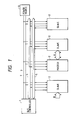
- FIG. 1 of the accompanying drawings shows a schematic block diagram of such an arrangement, which a plurality of circuit devices 2 are interconnected to a bus controller via a bus. That bus comprises an address and/or data bus (communication bus) 5, a control bus 4, and power buses 3,7 connected to a power source 6.
- One of the circuit devices 2 is a master, which controls the other circuit devices 2 which act as slaves.
- the master circuit device signals to that slave, and to the bus controller, via the control bus 4, and then data can be passed between master and slave along the address and data bus 5 as indicated by arrow A.
- the bus controller 1 ensures that the signalling is controlled in the desired way.
- US 4079440 proposes a system in which each circuit device is mounted on a printed circuit board, and the board has at least two connector plugs for connecting it to the power supply, with those plugs being of different lengths. Therefore, during insertion and removal, the time of contact with the power line of those two connector plugs is different, and this difference can be used to decrease fluctuations of the power source voltage during insertion and removal.
- this is only a limited solution to the problem, since it does not resolve all the causes of faulty signalling.
- US 4200865 discloses an arrangement in which the circuit devices are again mounted on a printed circuit board for insertion into a bus network, and the circuit board is designed so that the input to or the output from the board can be locked in response to the presence of two conditions, namely the application of a request for removal or insertion, and the fact that the circuit device is not signalling to any other device.
- the circuit components of the circuit device are connected to an address bus via an output driver, and the aim of the disclosure of US 4200865 is to lock that bus driver to prevent the bus line from being electrically disturbed.
- the present invention seeks to overcome, or at least ameliorate, the problems of the prior art by reducing or eliminating the risk of faults in signalling when a circuit device (which may be mounted on a printed circuit board) is inserted or removed into a bus network interconnecting a plurality of such devices.
- the present invention proposes that, on insertion, the first step is for the circuit device to generate a signal which prevents the other circuit devices (which are under power) from signalling on the communication bus of the bus network, and then powering the output driver of the circuit device. The signal is maintained until the output driver is stabilised, and it can then be removed. Similarly, on removal, a signal is supplied to the bus network to inhibit other circuit devices from transmitting, the power is removed from the output driver, the signal maintained until the output driver is stable, and only then is the circuit device removed. To express this in another way, the invention proposes that, on insertion or removal, the circuit device to be inserted or removed "occupies" the bus until insertion or removal is complete.
- the signalling described above will be controlled by a suitable control device in the circuit device. That control device controls the signalling to the bus network, and also controls the switching of power to the output driver in timed relationship with that signal.
- the act of physically inserting or removing the circuit device connects both the control circuit and the output driver physically to the bus network, but the device is arranged so that only the control device (and possibly other circuit components, but not including the output driver), be powered immediately on insertion. Then, the signal is generated to inhibit other devices from signalling on the communications bus, and then the output driver can be powered. Once the powering is stable, the circuit device may operate normally. On removal, the procedure is similar, with the powering of the control device remaining until the disconnection of the output driver is complete.
- the present invention has a number of aspects. It is concerned with the method and removal of a circuit device into a bus network having a plurality of powered circuit devices, to a circuit network having a plurality of such circuit devices interconnected by a bus network, to a method of maintaining such a circuit network, to the circuit device itself and to a computer system incorporating the network.
- the bus network and in particular the communication bus of that network, is not disturbed during insertion or removal of a circuit device, since the bus is effectively "occupied" by that device and other devices cannot be signalling on the bus. Occupation of the bus is released when the supply of power to the output driver is stabilised on disconnection and removal, and this enables the bus occupation time to be minimised.
- Figure 2 illustrates the connection of a circuit device to a bus network.
- the bus network shown in Figure 2 is the same as that in Figure 1, and furthermore further circuit devices 2 may also be connected to the bus network in a similar manner to that illustrated in Figure 1.
- the circuit device 2 comprises an electronic circuit 29 which contains the circuit components which define the operation to be carried out by the device 2. That electronic circuit 29 is connected via an interface circuit 28 to an output driver (bus driver) 21, which in turn is connected to the data bus (communications bus) 5. Thus, the electronic circuit 29 can signal via the interface circuit 28 and the bus driver 21 to the address bus. Similarly, signals from other circuit devices transmitted on the address bus 5 may be received via an address data receiver 26, which is connected to the interface circuit 28 and so permits those signals to be transmitted to the circuit 29.
- an output driver bus driver
- the circuit device 2 is also connected to the control bus 4 via a bus access controller 27. Connected to that access controller 27 is a active line insertion/removal controller (control device) 20 which controls the operation of the circuit device 2 in a manner which will be described.
- a bus access controller 27 Connected to that access controller 27 is a active line insertion/removal controller (control device) 20 which controls the operation of the circuit device 2 in a manner which will be described.
- the circuit device 2 is connected to the power source 6 via power buses 3 and 7, and the signal from those power buses passes via a switch 23 to the control device 20, to the interface circuit 28, and to the circuit 29.
- that switch 23 passes to the output driver 21 and to the data receiver 26, but interposed therebetween is a relay 22 controlled by the control device 20.
- a switch 24 is also connected to the control device 20, as is an LED (display) 25.
- circuit device 2 is to be removed from the bus network.
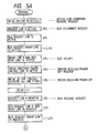
- the first stage is that switch 24 is opened, as shown in Figure 3, to generate a signal via line 16 to the control device 20.
- That control device then generates a signal via line 8 to the access controller 27, which in turn generates a signal (bus request) via line 12 to the control bus 4.
- That signal signals to the bus controller that the circuit device 2 to be removed is to "occupy" the bus, i.e. that other circuit devices connected to the bus network should not be permitted to transmit.
- the bus controller determines a time when no other circuit device is signalling, and transmits a signal (bus request grant) via the control bus 4 which is received on line 13 to the access controller 27. It is this signal that indicates that the circuit device 2 to be removed "occupies" the bus. The signal is passed via line 9 to the control device 20.
- the control device 20 On receipt of this signal, the control device 20 generates a signal on line 10 which opens the relay 22 and so cuts off the power from the output driver 21 and the data receiver 26. Effectively, line 11 is disconnected from the power supply whilst power to the other parts of the circuit device 2 remains.
- the control device 20 generate a signal (bus busy) which is fed via line 19, the access controller 27, and line 14 to the control bus 4.
- control device 20 simply to wait for a predetermined time t1, which is known to be longer than the unstable time of the output driver 21 before operating further.
- means may be provided to detect the state of the output driver 21 and signal to the control device 20 when the output driver 21 is in a stable state (at zero power on removal).
- control device 20 After the output driver 21 becomes stably off, the control device 20 removes the signal via lines 12 and 14 to the bus controller, thereby indicating that the device 2 no longer needs to occupy the data bus.
- the control device 20 generates a signal on line 17 to the LED 25, which is illuminated to show that the circuit device 2 is ready for removal.
- the switch 23 is opened to disconnect the control device 20, and the other parts of the circuit device 2 from the power supply, and then the circuit device 2 may be physically removed from the bus network.
- a signal is sent from the bus controller 1 and is received on line 13, and an appropriate signal sent via line 9 to the controller, generating a bus occupancy signal on line 19 and via the access controller 27 and line 14 to indicate to the other circuit devices that the bus network is occupied.
- the processing must then halt until the power to the output driver is stable, and again this may be for a predetermined time t1 or by some suitable detection.
- the control device 20 sends a signal via line 8, which is transmitted via the access controller 27 and line 12 to the control bus 4, and hence to the bus controller 1, to signal that the newly inserted circuit device 2 no longer needs to occupy the network.
- the signals are removed from lines 12 and 14, and the return signal from the bus controller 1 received on line 13 signals to the control device 20 to activate the LED 25.
- switch 24 is closed, and the control device 20 then cuts off the power to the LED 25. Insertion is then complete.
- Figs. 3 and 4 illustrate how, during the unstable period of the output driver 21 and data receiver 26, a bus occupy signal is supplied.
- Figure 7 corresponds to Figure 2, but shows the control device 20 in more detail.
- the controller 20 comprises a sequence controller 25 which determines the timing of the operation of the controller 20, three flip-flops 206, 207, 208 connected to transistor switches 200, 201, 202 and also connected via a logic gate 214 and amplifier 215 to the LED 25.
- the relay 203 is activated and the transistors 200 to 202 are all turned on. Therefore, the contact point of the relay 204 is off and the contact point of the relay 22 is on.
- a closed circuit for holding the relay 22 is formed via Vcc ⁇ coil 203A ⁇ contact point A 203B ⁇ transistor 200 even when the switch 24 is turned off, and the relay 203 maintains itself.
- the relay 203 is not excited when the power supply Vcc is interrupted or when the transistor 200 is turned off.
- the switch 24 is turned off, first (step (a) in Fig. 8).
- the output driver 21 When the switch 24 is turned off, the output driver 21 generates a bus occupation request REQ which is sent to the bus controller 1 via bus 5 (step (b) in Fig. 8).
- the bus controller 1 sends a bus occupation permission (REQG) to the circuit device (step (c)).
- the circuit device 2 then sends a BUS BUSY signal to the bus 4 from the gate 210A that indicates the bus occupation (step (d)).
- the circuit device 2 is allowed to occupy the bus.
- the flip-flop 208 When the bus is occupied, the flip-flop 208 produces an output Q at the L level to turn the transistor 202 off (step (e)).
- the transistor 202 that is turned off causes the contact of the relay 22 to be turned off (step (f)) and the feed of power to the bus driver 21 is interrupted.
- the output driver 21 With the feed of power being interrupted, the output driver 21 is powered down, with a slight delay in time. This is due to delay in mechanical operation of the relay 205, since it is an electromagnetic switch. The time is slightly delayed even when a transistor switch is used instead of the relay 205, and the same idea holds true.
- the output driver 21 is unstable (step (g)). After this unstable period, the gate 210A produces a BUS BUSY signal at the L level (step (h)).
- the flip-flop 207 produces an output Q at the L level to turn the transistor 201 off (step (i)). Therefore, the contact of the relay 204 is turned on to lock the driver 210 and the output of the gate 210A. Further, the flip-flop 206 produces the output Q at the L level to turn the transistor 200 off (step (j)). Accordingly, the relay 203 is not activated, and all the contacts of the relay 203 including the contact 203A are turned off (step (k)). Thus, the electric power is not fed to the relays 204, 205, nor to driver 210, or gate 210A of the access controller 27. The power feed switch 23 is then turned off. The feed of power to the circuit device 2 is now completely cut off; i.e., the circuit device 2 can be removed under the condition where the feed of power is completely stopped.
- the circuit device 2 is inserted after the switch 24 is turned off. After insertion, the power feed switch 23 is turned on (step (a)). Then, the flip-flops 206 to 208 produce outputs Q at the L level to turn the switch 209 on (step (b)). At this moment, since the flip-flop 206 produces an output Q at the L level, the transistor 200 is turned off and the relay 203 is not excited.
- the flip-flop 206 then produces an output Q at the H level, and the relay 203 is excited to turn the contact points on (step (c)). Therefore, power Vcc is fed to the relays 204, 205, driver 210 for bus control signal, and to gate 210A.
- Flip-flop 207 then produces an output Q at the H level (step (d)) to turn the transistor 201 on, to turn the contact B of the relay 204 off (step (e)), and to release the driver 210 for bus control signal and the gate 210A from the locked condition. Since the driver 210 and 210A are released from the locked condition, the circuit device 2 sends a bus occupation request REQ (step (h)) to the bus via driver 27. As for the case of removal, the circuit device 2 occupies the bus (generates BUSY signal, step (j)) under the condition where the bus is not occupied by any other circuit device.
- the flip-flop 208 produces an output Q at the H level (step (f)), whereby the transistor 202 is turned on, power is fed to the output driver 21 (step (k)), when the output driver 21 is stable (step (c)) the BUSY signal that indicates the condition of bus occupation is not produced (step (j)), and the insertion is completed.
- relays 203, 204 and 205 are used. However, it is also allowable to use electronic switches such as transistors in their place. This can be adapted to a system having a bus occupation monitoring time shorter than that of the relays.
- FIG. 10 the assembly of a plurality of output devices into a network corresponding to Figure 1, and their mounting in a computer will now be described.
- a plurality of circuit boards 300,301 are mounted in a frame 302.
- One of those circuit boards 300 may house the bus controller, and circuit board 301 illustrates a circuit board on which an output device 2 corresponding to the present invention is inserted, connected via suitable physical sockets 303,304 to the bus network shown at 4 and 5.
- the frame 302 is mounted in a housing 305, which also contains the power supply 6.
- Figure 10 also illustrates the two visible external switches 23,24 of the circuit device 2, and the LED 25. Those switches 23,24 form the user operated controls during removal and insertion as has been described above.
- circuit devices can be inserted or removed from a powered network without affecting other circuit devices connected to th at network. Maintenance of the system is rendered more simple, since a faulty board can be removed easily and a new board inserted. Poewr need not be interrupted during removal of a faulty board, so that the operation of a computer system incorporating such output devices need not be stopped, which also improves reliability.
- the circuit devices are normally mounted on a printed circuit board, for ease of handling.
Abstract
A circuit device 2 (e.g. mounted on a printed circuit board) is connected to data network, to which network are also connected a plurality of other circuit devices 2 under power. On removal of such a circuit device 2, the output driver 21 connecting the circuit components 28,29 of the output device 2 to the communications bus 5 of the bus network is first disconnected from power, and only when its disconnection is stable is the circuit device 2 withdrawn. A control device device 20 of the circuit device 2 is connected to the control bus 4 of the data network, and before power is disconnected from the output driver 21, the control device 20 signals to the network so as to prevent other circuit devices 2 connected to the network from signalling on the network. Effectively, the circuit device 2 to be removed "occupies" the bus. This occupation is maintained until the disconnection of the ouput driver 21 is stable, and then the circuit device 2 can be removed from the network. Similarly, on insertion, the network is first occupied before power is connected to the output driver 21. In this way, it becomes possible to prevent faults due to mis-signalling between the other circuit devices connected to the network when one circuit device is inserted or removed.
Description
- The present invention relates to the insertion and removal of a circuit device into a bus network. It is particularly, but not exclusively, concerned with the case where that circuit device is a printed circuit board.
- It is well known to interconnect the circuit devices by a bus network which enables the devices to signal one to the other. Fig. 1 of the accompanying drawings shows a schematic block diagram of such an arrangement, which a plurality of
circuit devices 2 are interconnected to a bus controller via a bus. That bus comprises an address and/or data bus (communication bus) 5, acontrol bus 4, andpower buses power source 6. One of thecircuit devices 2 is a master, which controls theother circuit devices 2 which act as slaves. When themaster circuit device 2 wishes to signal to one of theslave circuit devices 2, the master circuit device signals to that slave, and to the bus controller, via thecontrol bus 4, and then data can be passed between master and slave along the address anddata bus 5 as indicated by arrow A. Thebus controller 1 ensures that the signalling is controlled in the desired way. - However, it sometimes occurs that there is a failure in one of the components of the circuit, and then the
appropriate circuit device 2 must be removed and replaced. Where it is the master circuit device that is removed, there is normally no problem since the removal of that device effectively stops the network operating. However, when a slave circuit device is to be removed the position is more complicated. It is normally not desired completely to shut-down the network before removal of any particular circuit device, and therefore the faulty circuit device must be removed whilst the system remains under power. If one of thecircuit devices 2, e.g that indicated by arrow B is removed, then it is found that there is a risk that transient signals generated when it is removed affect data which may be being transmitted between the master and another of the slave devices. The present invention, therefore, is concerned with trying to overcome this problem, and permit insertion or withdrawal of a circuit device when the system is on-line (i.e. without disconnecting the power source) rather than by complete shut-down of the network. - US 4079440 proposes a system in which each circuit device is mounted on a printed circuit board, and the board has at least two connector plugs for connecting it to the power supply, with those plugs being of different lengths. Therefore, during insertion and removal, the time of contact with the power line of those two connector plugs is different, and this difference can be used to decrease fluctuations of the power source voltage during insertion and removal. However, this is only a limited solution to the problem, since it does not resolve all the causes of faulty signalling.
- US 4200865 discloses an arrangement in which the circuit devices are again mounted on a printed circuit board for insertion into a bus network, and the circuit board is designed so that the input to or the output from the board can be locked in response to the presence of two conditions, namely the application of a request for removal or insertion, and the fact that the circuit device is not signalling to any other device. In this system, the circuit components of the circuit device are connected to an address bus via an output driver, and the aim of the disclosure of US 4200865 is to lock that bus driver to prevent the bus line from being electrically disturbed.
- However, it has been discovered that the arrangement of US 4200865 has a problem. At the time the circuit device is inserted or removed, the power connection to the output driver is disconnected, and therefore its locking is no longer stable. As a result, during transient conditions at insertion or removal, the output driver may become unlocked and, depending on the electronic conditions present elsewhere in the circuit device, the circuit device may again be free to transmit to the bus network, thereby causing faults within the signalling in that network.
- The present invention seeks to overcome, or at least ameliorate, the problems of the prior art by reducing or eliminating the risk of faults in signalling when a circuit device (which may be mounted on a printed circuit board) is inserted or removed into a bus network interconnecting a plurality of such devices.
- At its most general, the present invention proposes that, on insertion, the first step is for the circuit device to generate a signal which prevents the other circuit devices (which are under power) from signalling on the communication bus of the bus network, and then powering the output driver of the circuit device. The signal is maintained until the output driver is stabilised, and it can then be removed. Similarly, on removal, a signal is supplied to the bus network to inhibit other circuit devices from transmitting, the power is removed from the output driver, the signal maintained until the output driver is stable, and only then is the circuit device removed. To express this in another way, the invention proposes that, on insertion or removal, the circuit device to be inserted or removed "occupies" the bus until insertion or removal is complete.
- Normally, the signalling described above will be controlled by a suitable control device in the circuit device. That control device controls the signalling to the bus network, and also controls the switching of power to the output driver in timed relationship with that signal.
- It is normal for the power supply to the circuit devices to come from power buses of the bus network. In this case, the act of physically inserting or removing the circuit device connects both the control circuit and the output driver physically to the bus network, but the device is arranged so that only the control device (and possibly other circuit components, but not including the output driver), be powered immediately on insertion. Then, the signal is generated to inhibit other devices from signalling on the communications bus, and then the output driver can be powered. Once the powering is stable, the circuit device may operate normally. On removal, the procedure is similar, with the powering of the control device remaining until the disconnection of the output driver is complete.
- The present invention has a number of aspects. It is concerned with the method and removal of a circuit device into a bus network having a plurality of powered circuit devices, to a circuit network having a plurality of such circuit devices interconnected by a bus network, to a method of maintaining such a circuit network, to the circuit device itself and to a computer system incorporating the network.
- With the present invention the bus network, and in particular the communication bus of that network, is not disturbed during insertion or removal of a circuit device, since the bus is effectively "occupied" by that device and other devices cannot be signalling on the bus. Occupation of the bus is released when the supply of power to the output driver is stabilised on disconnection and removal, and this enables the bus occupation time to be minimised.
- An embodiment of the invention will now be described in detail, by way of example, with reference to the accompanying drawings in which:
- Figure 1 shows a plurality of circuit components interconnected by a bus network, and has already been described;
- Figure 2 shows a general schematic view of a circuit device according to the present invention connected to a bus network;
- Figure 3 shows the operation of the device of Figure 2 during removal of that device from the network;
- Figure 4 shows the operation of that device during insertion;
- Figure 5 is a flow chart showing the steps during removal of the device of Figure 2 from the bus network;
- Figure 6 is a flow chart of the insertion of the circuit device of Figure 2 into the bus network;
- Figure 7 is a more detailed circuit diagram of the device shown in Figure 2;
- Figure 8 shows in more detail the operation of the circuit device of Figure 7, during removal of that device;
- Figure 9 shows in more detail the operation of the circuit device of Figure 7 during insertion of that device; and
- Figure 10 shows a computer system incorporating a plurality of circuit devices each corresponding to that shown in Figure 2.
- In the drawings corresponding parts are indicated by the same reference numerals.
- Figure 2 illustrates the connection of a circuit device to a bus network. The bus network shown in Figure 2 is the same as that in Figure 1, and furthermore
further circuit devices 2 may also be connected to the bus network in a similar manner to that illustrated in Figure 1. - The
circuit device 2 comprises anelectronic circuit 29 which contains the circuit components which define the operation to be carried out by thedevice 2. Thatelectronic circuit 29 is connected via aninterface circuit 28 to an output driver (bus driver) 21, which in turn is connected to the data bus (communications bus) 5. Thus, theelectronic circuit 29 can signal via theinterface circuit 28 and thebus driver 21 to the address bus. Similarly, signals from other circuit devices transmitted on theaddress bus 5 may be received via anaddress data receiver 26, which is connected to theinterface circuit 28 and so permits those signals to be transmitted to thecircuit 29. - The
circuit device 2 is also connected to thecontrol bus 4 via abus access controller 27. Connected to thataccess controller 27 is a active line insertion/removal controller (control device) 20 which controls the operation of thecircuit device 2 in a manner which will be described. - The
circuit device 2 is connected to thepower source 6 viapower buses switch 23 to thecontrol device 20, to theinterface circuit 28, and to thecircuit 29. In addition, thatswitch 23 passes to theoutput driver 21 and to thedata receiver 26, but interposed therebetween is arelay 22 controlled by thecontrol device 20. Aswitch 24 is also connected to thecontrol device 20, as is an LED (display) 25. - The operation of the circuit device of Figure 2 will now be described, referring also to Figs. 3 and 4, and the flowchart of Figs. 5 and 6. Consider first the case where the
circuit device 2 is to be removed from the bus network. The first stage is thatswitch 24 is opened, as shown in Figure 3, to generate a signal vialine 16 to thecontrol device 20. That control device then generates a signal vialine 8 to theaccess controller 27, which in turn generates a signal (bus request) vialine 12 to thecontrol bus 4. That signal signals to the bus controller that thecircuit device 2 to be removed is to "occupy" the bus, i.e. that other circuit devices connected to the bus network should not be permitted to transmit. - On receipt of that signal, the bus controller determines a time when no other circuit device is signalling, and transmits a signal (bus request grant) via the
control bus 4 which is received on line 13 to theaccess controller 27. It is this signal that indicates that thecircuit device 2 to be removed "occupies" the bus. The signal is passed vialine 9 to thecontrol device 20. On receipt of this signal, thecontrol device 20 generates a signal online 10 which opens therelay 22 and so cuts off the power from theoutput driver 21 and thedata receiver 26. Effectively,line 11 is disconnected from the power supply whilst power to the other parts of thecircuit device 2 remains. At the same time, thecontrol device 20 generate a signal (bus busy) which is fed vialine 19, theaccess controller 27, and line 14 to thecontrol bus 4. - Once the power has been removed from the output driver 21 (and the data receiver 26) there is a short time of the order of 1µS to 100µS when the operation of the
output driver 21 is unstable. This time must elapse before any other change can be made. - It is possible for the
control device 20 simply to wait for a predetermined time t₁, which is known to be longer than the unstable time of theoutput driver 21 before operating further. Alternatively, means (not shown) may be provided to detect the state of theoutput driver 21 and signal to thecontrol device 20 when theoutput driver 21 is in a stable state (at zero power on removal). - After the
output driver 21 becomes stably off, thecontrol device 20 removes the signal vialines 12 and 14 to the bus controller, thereby indicating that thedevice 2 no longer needs to occupy the data bus. - Once the
circuit device 2 no longer occupies the line, thecontrol device 20 generates a signal online 17 to theLED 25, which is illuminated to show that thecircuit device 2 is ready for removal. At that time, theswitch 23 is opened to disconnect thecontrol device 20, and the other parts of thecircuit device 2 from the power supply, and then thecircuit device 2 may be physically removed from the bus network. - The above steps are shown in Figs. 5a and 5b, in which the numerals indicate the component affected at any particular time.
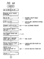
- On insertion of a new circuit component to the procedure is similar. The
circuit device 2 is inserted with theswitch 24 closed, and theswitch 23 open. This physically connects the circuit board to the data bus. Thus theswitch 23 is closed. This powers all parts of thecircuit device 2 except theoutput driver 21 anddata receiver 26. Once this happens, a signal is supplied vialine 16 to thecontrol device 20, causing thatcontrol device 20 to start the insertion activation procedure. The first stage is that a signal is sent vialine 8, theaccess controller 27 and theline 12 to thecontrol bus 4 and hence to the bus controller, to request that the newly insertedcircuit device 2 occupies the bus. On confirmation of this, a signal is sent from thebus controller 1 and is received on line 13, and an appropriate signal sent vialine 9 to the controller, generating a bus occupancy signal online 19 and via theaccess controller 27 and line 14 to indicate to the other circuit devices that the bus network is occupied. - Once this has been completed, a signal is sent from the
control device 20 vialine 10 to close therelay 22 and hence power theoutput driver 21 anddata receiver 26. - As before, the processing must then halt until the power to the output driver is stable, and again this may be for a predetermined time t₁ or by some suitable detection. Once that time has elapsed, the
control device 20 sends a signal vialine 8, which is transmitted via theaccess controller 27 andline 12 to thecontrol bus 4, and hence to thebus controller 1, to signal that the newly insertedcircuit device 2 no longer needs to occupy the network. At that time, the signals are removed fromlines 12 and 14, and the return signal from thebus controller 1 received on line 13 signals to thecontrol device 20 to activate theLED 25. On illumination of that LED, the insertion procedure is complete, switch 24 is closed, and thecontrol device 20 then cuts off the power to theLED 25. Insertion is then complete. - Also illustrated in Figure 2 is a
reset input 18 from thecontrol bus 4, which is used to reset all the components on insertion. - Figs. 3 and 4 illustrate how, during the unstable period of the
output driver 21 anddata receiver 26, a bus occupy signal is supplied. - Figure 7, corresponds to Figure 2, but shows the
control device 20 in more detail. The parts of the circuit are the same as shown in Figure 2. As shown in Figure 7, thecontroller 20 comprises asequence controller 25 which determines the timing of the operation of thecontroller 20, three flip-flops transistor switches amplifier 215 to theLED 25. - The operation of the device of Figure 7 will now be described, also referring to Figs 8 and 9 in which the various steps are shown.
- Again, the removal operation will be described first. Some of the steps will, of course, correspond to the earlier description of the operation of Figure 2, but for convenience will be duplicated where appropriate.
- Before the circuit device is removed, the
relay 203 is activated and the transistors 200 to 202 are all turned on. Therefore, the contact point of therelay 204 is off and the contact point of therelay 22 is on. When therelay 203 is activated, a closed circuit for holding therelay 22 is formed via Vcc →coil 203A → contact point A 203B → transistor 200 even when theswitch 24 is turned off, and therelay 203 maintains itself. Therelay 203 is not excited when the power supply Vcc is interrupted or when the transistor 200 is turned off. - At the time of removal, the
switch 24 is turned off, first (step (a) in Fig. 8). When theswitch 24 is turned off, theoutput driver 21 generates a bus occupation request REQ which is sent to thebus controller 1 via bus 5 (step (b) in Fig. 8). When no other printed circuit board is producing a bus occupation request, thebus controller 1 sends a bus occupation permission (REQG) to the circuit device (step (c)). Thecircuit device 2 then sends a BUS BUSY signal to thebus 4 from the gate 210A that indicates the bus occupation (step (d)). Thus, thecircuit device 2 is allowed to occupy the bus. - When the bus is occupied, the flip-
flop 208 produces an output Q at the L level to turn thetransistor 202 off (step (e)). Thetransistor 202 that is turned off causes the contact of therelay 22 to be turned off (step (f)) and the feed of power to thebus driver 21 is interrupted. With the feed of power being interrupted, theoutput driver 21 is powered down, with a slight delay in time. This is due to delay in mechanical operation of the relay 205, since it is an electromagnetic switch. The time is slightly delayed even when a transistor switch is used instead of the relay 205, and the same idea holds true. During this powering down, theoutput driver 21 is unstable (step (g)). After this unstable period, the gate 210A produces a BUS BUSY signal at the L level (step (h)). - Next, the flip-
flop 207 produces an output Q at the L level to turn thetransistor 201 off (step (i)). Therefore, the contact of therelay 204 is turned on to lock thedriver 210 and the output of the gate 210A. Further, the flip-flop 206 produces the output Q at the L level to turn the transistor 200 off (step (j)). Accordingly, therelay 203 is not activated, and all the contacts of therelay 203 including thecontact 203A are turned off (step (k)). Thus, the electric power is not fed to therelays 204, 205, nor todriver 210, or gate 210A of theaccess controller 27. Thepower feed switch 23 is then turned off. The feed of power to thecircuit device 2 is now completely cut off; i.e., thecircuit device 2 can be removed under the condition where the feed of power is completely stopped. - Insertion will now be described in conjunction with Fig. 9. The
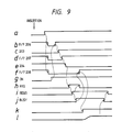
circuit device 2 is inserted after theswitch 24 is turned off. After insertion, thepower feed switch 23 is turned on (step (a)). Then, the flip-flops 206 to 208 produce outputs Q at the L level to turn the switch 209 on (step (b)). At this moment, since the flip-flop 206 produces an output Q at the L level, the transistor 200 is turned off and therelay 203 is not excited. - The flip-
flop 206 then produces an output Q at the H level, and therelay 203 is excited to turn the contact points on (step (c)). Therefore, power Vcc is fed to therelays 204, 205,driver 210 for bus control signal, and to gate 210A. - Flip-
flop 207 then produces an output Q at the H level (step (d)) to turn thetransistor 201 on, to turn the contact B of therelay 204 off (step (e)), and to release thedriver 210 for bus control signal and the gate 210A from the locked condition. Since thedriver 210 and 210A are released from the locked condition, thecircuit device 2 sends a bus occupation request REQ (step (h)) to the bus viadriver 27. As for the case of removal, thecircuit device 2 occupies the bus (generates BUSY signal, step (j)) under the condition where the bus is not occupied by any other circuit device. - After the bus is occupied, the flip-
flop 208 produces an output Q at the H level (step (f)), whereby thetransistor 202 is turned on, power is fed to the output driver 21 (step (k)), when theoutput driver 21 is stable (step (c)) the BUSY signal that indicates the condition of bus occupation is not produced (step (j)), and the insertion is completed. - According to the arrangement shown in Fig. 7, relays 203, 204 and 205 are used. However, it is also allowable to use electronic switches such as transistors in their place. This can be adapted to a system having a bus occupation monitoring time shorter than that of the relays.
- Referring now to Figure 10, the assembly of a plurality of output devices into a network corresponding to Figure 1, and their mounting in a computer will now be described. Referring to Figure 10, a plurality of circuit boards 300,301 are mounted in a
frame 302. One of thosecircuit boards 300 may house the bus controller, andcircuit board 301 illustrates a circuit board on which anoutput device 2 corresponding to the present invention is inserted, connected via suitable physical sockets 303,304 to the bus network shown at 4 and 5. Theframe 302 is mounted in ahousing 305, which also contains thepower supply 6. Figure 10 also illustrates the two visibleexternal switches circuit device 2, and theLED 25. Those switches 23,24 form the user operated controls during removal and insertion as has been described above. - Thus, as has been described above, circuit devices can be inserted or removed from a powered network without affecting other circuit devices connected to th at network. Maintenance of the system is rendered more simple, since a faulty board can be removed easily and a new board inserted. Poewr need not be interrupted during removal of a faulty board, so that the operation of a computer system incorporating such output devices need not be stopped, which also improves reliability. The circuit devices are normally mounted on a printed circuit board, for ease of handling.
Claims (25)
1. A method of inserting a circuit device into a bus network having a plurality of powered circuit devices (2) interconnected by a communication bus (5) of said network, said method comprising:
connecting an output driver of said circuit device (2) to said communication bus (5), said output driver being unpowered; and
powering said output driver (21) from a power supply;
characterised in that
prior to powering of said output driver (21), a signal is generated from said circuit device (2) to prevent said powered circuit devices (2) from signalling to said communication bus (5); and
the signal is removed subsequent to the powering of said output driver (21).
2. A method according to claim 1, wherein said circuit device (2) includes a control circuit (20) for generating said signal, and said control circuit (20)is connected to said network simultaneously with the connecting of said output driver (21).
3. A method according to claim 1 or claim 2, wherein said circuit device (2) includes a control circuit (20) for generating said signal, and said control circuit (20) is connected to said power supply (6,7) prior to the generation of said signal.
4. A method according to claim 3 wherein said circuit device (2) further includes a plurality of circuit components (21,24) for connection to said communication bus (5) via said output driver (21), and said plurality of circuit components (28,29) are connected to said power supply (6,7) simultaneously with said control circuit (20).
5. A method of removing a circuit device from a bus network having a plurality of powered circuit devices (2) and said circuit device (2) interconnected by a communication bus (5) of said network, said method comprising:
removing the power supply from an output driver (21) of said circuit device, which output driver (21) is connected to said communication bus (5); and
disconnecting said output driver from said communication bus (5).
characterised in that:
prior to removal of the power from the output driver (21), a signal is generated from said circuit device (2) to prevent said powered circuit devices (2) from signalling to said communication bus (5);
6. A method according to claim 5, wherein said circuit device (2) includes a control circuit (20) for generating said signal, and said control circuit (20) is disconnected from said network simultaneously with the disconnecting of said output driver (21).
7. A method according to claim 5 or claim 6, wherein said circuit device includes a control circuit (20) for generating said control signal, and said control circuit (20) is disconnected from said power supply (6,7) subsequent to the removing of said signal.
8. A method according to claim 7, wherein said circuit device further includes a plurality of circuit components (28,29) connected to said communication bus (5) via said output driver (21), and said plurality of circuit components (28,29) are disconnected from said power supply (6,7) simultaneously with said disconnecting of said control circuit (20).
9. A method of inserting a circuit device (2) into a bus network having a plurality of powered circuit devices (2) interconnected by a communication bus (5) of said network, said method comprising:
connecting said circuit device (2) to said network;
characterised in that: during said connecting, a signal is generated for a predetermined period to prevent said powered circuit devices (2) from signalling to said communication bus (5), and an output driver (21) of said circuit device is powered during said predetermined period.
10. A method of removing a circuit device from a bus network having a plurality of powered circuit devices (2) and said circuit device (2) interconnected by a communication bus (5) of said network, said method comprising:
disconnecting said circuit device (2) from said network;
characterised in that: during said disconnecting, a signal is generated for a predetermined period to prevent said powered circuit devices (2) from signalling to said communication bus, and an output driver (21) of said circuit device (2) is disconnected from power during said predetermined period.
11. A method of inserting a circuit device into a bus network having a plurality of powered circuit devices (2) interconnected by a communication bus (5) of said network, said method comprising:
connecting said circuit device (2) to said network;
characterised in that: during said connecting, a signal is generated to prevent said powered circuit devices (2) from signalling to said communciation bus (5), and an output driver (21) of said circuit device is powered, said signal being maintained at least until the powering of said output driver (21) is stabilized.
12. A method of removing a circuit device from a bus network having a plurality of powered circuit devices (2) and said circuit device (2) interconnected by a communication bus (5) of said network, said method comprising:
disconnecting said circuit device (2) from said network;
wherein, during said disconnecting, a signal is generated to prevent said powered circuit devices (2) from signalling to said communication bus (5), and an output driver (21) of said circuit device is disconnected from power, said signal being maintained until the disconnection of said output driver (21) is stabilized.
13. A method according to any one of the preceding claims, wherein said bus network includes a signal bus (4) interconnecting said powered circuit devices (2) and said signal is applied to said signal bus (4).
14. A circuit network having a plurality of first circuit devices (2), a bus network including a communication bus (5) interconnecting said first circuit devices, and a second circuit device (2) for connection to said bus network,
said second circuit device comprising:
an output driver (21) for connection to said communication bus (5); and
a connection means (22) for connecting said output driver (21) to a power source (6,7);
characterized in that:
the second circuit device (2) further includes a control circuit (20) for connection to said bus network and for controlling said connection means (22), said control circuit (20) being arranged to generate a first signal to said network for preventing said first circuit devices (2) from signalling to said communication bus (5), and subsequently to generate a second signal for causing said connection means (22) to connect said output driver (21) to said power source (6,7).
15. A circuit network having a plurality of circuit devices (2) and a bus network including a communication bus (5) interconnecting said circuit devices (2), wherein at least one of said circuit devices is arranged to be removed from said network;
said at least one circuit device comprising:
an output driver connected to said communication bus; and
a connection means (22) connecting said output driver (21) to a power source (6,7);
characterized in that:
said at least one circuit device further comprises
a control circuit (20) connected to said network for controlling said connecting means (22), said control circuit (20) being arranged to generate a first signal to said network for preventing said circuit devices other than said at least one circuit device from signalling to said communication bus (5), and subsequently to generate a second signal for causing said connection means (22) to disconnect said output driver (21) from said power source (6,7).
16. A circuit network having a plurality of first circuit devices (2), a bus network including a communication bus (5) interconnecting said first circuit devices, and a second circuit device (2) for connection to said bus network,
said second circuit device comprising:
an output driver (21) for connection to said communication bus (5); and
a connection means (22) for connecting said output driver (21) to a power source (6,7);
characterised in that:
said connection means is arranged to connect said output driver to said power source only when said first circuit devices are prevented from signalling to said communication bus.
17. A circuit network having a plurality of circuit devices (2) and a bus network including a communication bus (5) interconnecting said circuit devices (2), wherein at least one of said circuit devices is arranged to be removed from said network;
said at least one circuit dfevice comprising:
an output driver connected to said communication bus; and
a connection means (22) connecting said output driver (21) to a power source (6,7);
characterised in that:
said connection means is arranged to disconnect said output driver from said power source only when said circuit devices other than said at least one circuit device are prevented from signalling to said communication bus.
18. A circuit network according to ny one of claims 13 to 16, wherein said network includes a control bus (4) interconnecting said circuit devices (2), and said control circuit (20) is connected to said control bus (4).
19. A circuit network according to any one of claims 13 to 17, wherein said at least one circuit device further includes a plurality of circuit components (28,29) connected to said communication bus (5) via said output driver (21), and a further connection means (23) connecting said control circuit (20) and said plurality of circuit components to said power supply (6,7).
20. A circuit network according to any one of claims 13 to 18, wherein said at least one circuit device is a printed circuit board.
21. A method of maintaining a circuit network having a plurality of powered circuit devices (2), including a faulty circuit device, and a bus network including a communication bus (5) interconnecting said circuit devices (2), said method comprising:
removing said faulty circuit device;
connecting a new circuit device to said bus network to replace said faulty device; and
powering said new circuit device;
characterised in that:
preventing prior to removal of the faulty circuit device said powered circuit devices other than said faulty circuit device are prevented from signalling on said communication bus (5) whilst maintaining the power there to; and
subsequent to the powering of the new circuit device said powered circuit devices, other than said faulty circuit device, and said new circuit device are permitted to signal on said communication bus (5).
22. A method according to claim 20, wherein, after said removing of said faulty circuit device, said powered circuits other than said faulty circuit device are permitted to signal on said communication bus (5) and, prior to said connecting of said new circuit device, said powered circuits other than said faulty circuit are again prevented from signalling on said communication bus (5).
23. A circuit device for connection to a bus network, comprising:
an output driver (21);
a plurality of circuit components (28,29) for connection to said bus network via said output driver (21);
characterised in that:
the circuit device further includes:
a control circuit (20);
first switching means (23) for connecting said plurality of circuit components (28,29) and said control circuit (20) to a power supply (6,7); and
second switching means (22) controllable by said control circuit (20) for connecting said output driver (21) to said power supply (6,7);
wherein activation of said first switching means (23) is arranged to activate said control means (20), and said control means (20) is arranged subsequently to activate said second switching means (22) thereby to activate said output driver (21).
24. A circuit device for connection to and removal from a bus network comprising:
a plurality of circuit components (28,29);
an output driver (21) for connecting said circuit components (28,29) to said network;
a first user operable switch (24) for generating a removal signal;
characterized in that:
the device further includes a control circuit (20) for receiving said removal signal and for disconnecting said output driver (21) from a power supply (6,7);
a display (25) for indicating the completion of said disconnectlng of said output driver (21); and
a second user operable switch (23) for disconnecting said control circuit (20) and said plurality of circuit components (28,29) from said power supply (6,7).
25. A computer system comprising:
a bus network including a communication bus (5);
a bus controller (1) connected to said bus network; and
a plurality of circuit devices (2) connected to said network and arranged to signal on said communication bus (5) under control of said bus controller (1), each of said circuit devices (2) including an output driver (21) and a plurality of other components (28,29);
characterized in that:
at least some of said plurality of circuit devices (2) are each arranged to generate a first signal to said bus controller (1), each of said first signals being arranged to prevent any other circuit device other than the one circuit device generating one said first signal from signalling to said communication bus (5), and said bus controller (1) is arranged to generate a second signal in response to said first signal for causing the output driver of said one circuit device to be disconnected from a power supply (6,7) without disconnection of the other components (28,29) of said one circuit device.
Applications Claiming Priority (2)
| Application Number | Priority Date | Filing Date | Title |
|---|---|---|---|
| JP171779/88 | 1988-07-12 | ||
| JP17177988 | 1988-07-12 |
Publications (2)
| Publication Number | Publication Date |
|---|---|
| EP0352934A2 true EP0352934A2 (en) | 1990-01-31 |
| EP0352934A3 EP0352934A3 (en) | 1990-04-25 |
Family
ID=15929524
Family Applications (1)
| Application Number | Title | Priority Date | Filing Date |
|---|---|---|---|
| EP89307046A Withdrawn EP0352934A3 (en) | 1988-07-12 | 1989-07-11 | Insertion and removal of a circuit device into a bus network |
Country Status (3)
| Country | Link |
|---|---|
| US (1) | US5247619A (en) |
| EP (1) | EP0352934A3 (en) |
| JP (1) | JPH02125314A (en) |
Cited By (3)
| Publication number | Priority date | Publication date | Assignee | Title |
|---|---|---|---|---|
| FR2671887A1 (en) * | 1991-01-21 | 1992-07-24 | Systolic Sarl | Electronic device allowing the connection and disconnection of a bus line of a computer system |
| EP0548382A1 (en) * | 1991-12-20 | 1993-06-30 | Siemens Nixdorf Informationssysteme Aktiengesellschaft | Method and device for on-line exchanging of circuit modules in a bus system |
| EP0559454A1 (en) * | 1992-03-06 | 1993-09-08 | Data General Corporation | On-line module replacement in a multiple module data processing system |
Families Citing this family (25)
| Publication number | Priority date | Publication date | Assignee | Title |
|---|---|---|---|---|
| JP2752247B2 (en) * | 1990-11-29 | 1998-05-18 | 富士通株式会社 | Information storage device |
| JPH05204785A (en) * | 1992-01-29 | 1993-08-13 | Fujitsu Ltd | System, method, and device for protecting monitor bus |
| US5678197A (en) * | 1993-02-26 | 1997-10-14 | Motorola, Inc. | Method for reprogramming a communication unit's access to a wireless communication system |
| JP2636141B2 (en) * | 1993-07-09 | 1997-07-30 | 日本電気株式会社 | Hot swapping method |
| US5579491A (en) * | 1994-07-07 | 1996-11-26 | Dell U.S.A., L.P. | Local proactive hot swap request/acknowledge system |
| US5555510A (en) * | 1994-08-02 | 1996-09-10 | Intel Corporation | Automatic computer card insertion and removal algorithm |
| JPH0895687A (en) * | 1994-09-26 | 1996-04-12 | Fujitsu Ltd | I/o card, connecting cable to be connected with the i/o card and power saving method for i/o card |
| US5586271A (en) * | 1994-09-27 | 1996-12-17 | Macrolink Inc. | In-line SCSI bus circuit for providing isolation and bi-directional communication between two portions of a SCSI bus |
| KR970010634B1 (en) * | 1994-10-25 | 1997-06-28 | 삼성전자 주식회사 | Metwork hibernation system |
| US5581712A (en) * | 1994-11-17 | 1996-12-03 | Intel Corporation | Method and apparatus for managing live insertion of CPU and I/O boards into a computer system |
| JP2682503B2 (en) * | 1995-03-24 | 1997-11-26 | 日本電気株式会社 | Hot-swap system |
| KR0151663B1 (en) * | 1995-05-17 | 1998-10-15 | 김광호 | Docking station for portable pc |
| US5740378A (en) * | 1995-08-17 | 1998-04-14 | Videoserver, Inc. | Hot swap bus architecture |
| KR0156802B1 (en) * | 1995-11-07 | 1998-11-16 | 김광호 | Network hybernation system |
| US5974552A (en) * | 1995-12-29 | 1999-10-26 | Samsung Electronics Co., Ltd. | Method and apparatus for executing a scheduled operation after wake up from power off state |
| US5812798A (en) * | 1996-01-26 | 1998-09-22 | Motorola, Inc. | Data processing system for accessing an external device and method therefore |
| US5922060A (en) * | 1996-12-31 | 1999-07-13 | Compaq Computer Corporation | Expansion card insertion and removal |
| US5822196A (en) * | 1996-06-05 | 1998-10-13 | Compaq Computer Corporation | Securing a card in an electronic device |
| US6101322A (en) * | 1996-06-05 | 2000-08-08 | Compaq Computer Corporation | Removal and insertion of expansion cards in a computer system |
| US6098132A (en) * | 1996-06-05 | 2000-08-01 | Compaq Computer Corporation | Installation and removal of components of a computer |
| US6073196A (en) * | 1996-06-05 | 2000-06-06 | Compaq Computer Corporation | Using communication cycles for connecting and disconnecting devices in a computer system |
| US5943482A (en) * | 1996-06-05 | 1999-08-24 | Compaq Computer Corporation | Expansion card insertion and removal |
| KR100244778B1 (en) | 1997-07-19 | 2000-02-15 | 윤종용 | Hot insertion apparatus of board for state operation in system on-line state |
| US6032209A (en) * | 1998-07-24 | 2000-02-29 | Storage Technology Corporation | Hot-swappable high speed point-to-point interface |
| US6594721B1 (en) * | 2000-02-29 | 2003-07-15 | Hewlett-Packard Development Company, L.P. | Surprise hot bay swapping of IDE/ATAPI devices |
Citations (5)
| Publication number | Priority date | Publication date | Assignee | Title |
|---|---|---|---|---|
| US4200865A (en) * | 1977-02-02 | 1980-04-29 | Hitachi, Ltd. | Printed circuit board capable of being inserted and withdrawn on on-line status |
| US4510553A (en) * | 1983-01-24 | 1985-04-09 | Burroughs Corporation | Electromechanical assembly for aligning, discharging, and sequentially engaging conductors of a P.C. board with a backplane |
| DE3504560A1 (en) * | 1985-02-11 | 1986-08-14 | Siemens AG, 1000 Berlin und 8000 München | Arrangement for the connection of assemblies which can be pushed into mounting racks |
| EP0241905A2 (en) * | 1986-04-14 | 1987-10-21 | Siemens Nixdorf Informationssysteme Aktiengesellschaft | Circuit board for on-line insertion in computer system |
| EP0254456A2 (en) * | 1986-07-21 | 1988-01-27 | AT&T Corp. | Apparatus for controlled removal and insertion of circuit modules |
Family Cites Families (4)
| Publication number | Priority date | Publication date | Assignee | Title |
|---|---|---|---|---|
| US4562535A (en) * | 1982-04-05 | 1985-12-31 | Texas Instruments Incorporated | Self-configuring digital processor system with global system |
| US4635192A (en) * | 1983-12-06 | 1987-01-06 | Tri Sigma Corporation | Self configuring bus structure for computer network |
| US4704599A (en) * | 1984-06-20 | 1987-11-03 | Kimmel Arthur T | Auxiliary power connector and communication channel control circuit |
| US4609829A (en) * | 1984-08-23 | 1986-09-02 | Ncr Corporation | Apparatus for assisting in the connection and disconnection of a board with an energized circuit |
-
1989
- 1989-07-05 US US07/375,826 patent/US5247619A/en not_active Expired - Fee Related
- 1989-07-11 EP EP89307046A patent/EP0352934A3/en not_active Withdrawn
- 1989-07-12 JP JP1178114A patent/JPH02125314A/en active Pending
Patent Citations (5)
| Publication number | Priority date | Publication date | Assignee | Title |
|---|---|---|---|---|
| US4200865A (en) * | 1977-02-02 | 1980-04-29 | Hitachi, Ltd. | Printed circuit board capable of being inserted and withdrawn on on-line status |
| US4510553A (en) * | 1983-01-24 | 1985-04-09 | Burroughs Corporation | Electromechanical assembly for aligning, discharging, and sequentially engaging conductors of a P.C. board with a backplane |
| DE3504560A1 (en) * | 1985-02-11 | 1986-08-14 | Siemens AG, 1000 Berlin und 8000 München | Arrangement for the connection of assemblies which can be pushed into mounting racks |
| EP0241905A2 (en) * | 1986-04-14 | 1987-10-21 | Siemens Nixdorf Informationssysteme Aktiengesellschaft | Circuit board for on-line insertion in computer system |
| EP0254456A2 (en) * | 1986-07-21 | 1988-01-27 | AT&T Corp. | Apparatus for controlled removal and insertion of circuit modules |
Cited By (5)
| Publication number | Priority date | Publication date | Assignee | Title |
|---|---|---|---|---|
| FR2671887A1 (en) * | 1991-01-21 | 1992-07-24 | Systolic Sarl | Electronic device allowing the connection and disconnection of a bus line of a computer system |
| EP0548382A1 (en) * | 1991-12-20 | 1993-06-30 | Siemens Nixdorf Informationssysteme Aktiengesellschaft | Method and device for on-line exchanging of circuit modules in a bus system |
| US5378930A (en) * | 1991-12-20 | 1995-01-03 | Siemens Nixdorf Informationssysteme Ag | Method and arrangement for accomplishing assembly substitution actions during ongoing operation of a bus system |
| EP0559454A1 (en) * | 1992-03-06 | 1993-09-08 | Data General Corporation | On-line module replacement in a multiple module data processing system |
| US5371743A (en) * | 1992-03-06 | 1994-12-06 | Data General Corporation | On-line module replacement in a multiple module data processing system |
Also Published As
| Publication number | Publication date |
|---|---|
| JPH02125314A (en) | 1990-05-14 |
| US5247619A (en) | 1993-09-21 |
| EP0352934A3 (en) | 1990-04-25 |
Similar Documents
| Publication | Publication Date | Title |
|---|---|---|
| EP0352934A2 (en) | Insertion and removal of a circuit device into a bus network | |
| CA1283484C (en) | Method and apparatus for controlled removal and insertion of circuit modules | |
| US5051606A (en) | Method of connecting and disconnecting a board in a hot state | |
| EP1311958B1 (en) | Method and apparatus for removing and installing a computer system bus agent without powering down the computer system | |
| JP2669855B2 (en) | COMMUNICATION DEVICE, STAR CIRCUIT USED IN THE COMMUNICATION DEVICE, AND DEVICE COMPRISING THE STAR CIRCUIT | |
| US5293589A (en) | Circuit with predetermined delay for selectively relaying interrupt signals through a daisy-chain of linked modules upon removal of a module from a slot | |
| US5463663A (en) | Controlling synchronization in a system having a plurality of units when a unit is disconnected from or connected to the system that is active | |
| US6801973B2 (en) | Hot swap circuit module | |
| US6988157B2 (en) | Hot insertion of a service processor card in a system | |
| KR0122456B1 (en) | Mode detection method for hot back-up apparatus | |
| KR100369685B1 (en) | A method and a device of synchronization reference clock for exchanger | |
| KR100263510B1 (en) | Signal line interface for hot docking | |
| JPH0741619U (en) | Module connection mechanism for monitoring and control equipment | |
| JP3438431B2 (en) | Forced control unit for remote monitoring and control system | |
| JPH04336361A (en) | Data bus extension device | |
| KR0125889Y1 (en) | Double mode controller of plc | |
| KR0143971B1 (en) | Dual system | |
| JPH05265594A (en) | Uninterruptive computer | |
| KR100499501B1 (en) | duplexing apparatus and method | |
| JP3042522B1 (en) | Printed board difference detection mechanism | |
| JPH01112415A (en) | On-line repairing system | |
| JPH07182074A (en) | Hot-line insertion and pull-out device for hot standby type duplex system | |
| JPH059996B2 (en) | ||
| JPH08139712A (en) | Clock switching circuit | |
| JPS5972257A (en) | Communication controller |
Legal Events
| Date | Code | Title | Description |
|---|---|---|---|
| PUAI | Public reference made under article 153(3) epc to a published international application that has entered the european phase |
Free format text: ORIGINAL CODE: 0009012 |
|
| 17P | Request for examination filed |
Effective date: 19890828 |
|
| AK | Designated contracting states |
Kind code of ref document: A2 Designated state(s): DE GB |
|
| PUAL | Search report despatched |
Free format text: ORIGINAL CODE: 0009013 |
|
| AK | Designated contracting states |
Kind code of ref document: A3 Designated state(s): DE GB |
|
| 17Q | First examination report despatched |
Effective date: 19930303 |
|
| STAA | Information on the status of an ep patent application or granted ep patent |
Free format text: STATUS: THE APPLICATION IS DEEMED TO BE WITHDRAWN |
|
| 18D | Application deemed to be withdrawn |
Effective date: 19950201 |