EP0353633B1 - Supersonic flaw detecting system - Google Patents
Supersonic flaw detecting system Download PDFInfo
- Publication number
- EP0353633B1 EP0353633B1 EP89113876A EP89113876A EP0353633B1 EP 0353633 B1 EP0353633 B1 EP 0353633B1 EP 89113876 A EP89113876 A EP 89113876A EP 89113876 A EP89113876 A EP 89113876A EP 0353633 B1 EP0353633 B1 EP 0353633B1
- Authority
- EP
- European Patent Office
- Prior art keywords
- cursor
- supersonic
- scope image
- array elements
- signal
- Prior art date
- Legal status (The legal status is an assumption and is not a legal conclusion. Google has not performed a legal analysis and makes no representation as to the accuracy of the status listed.)
- Expired - Lifetime
Links
Images


Classifications
-
- G—PHYSICS
- G01—MEASURING; TESTING
- G01S—RADIO DIRECTION-FINDING; RADIO NAVIGATION; DETERMINING DISTANCE OR VELOCITY BY USE OF RADIO WAVES; LOCATING OR PRESENCE-DETECTING BY USE OF THE REFLECTION OR RERADIATION OF RADIO WAVES; ANALOGOUS ARRANGEMENTS USING OTHER WAVES
- G01S7/00—Details of systems according to groups G01S13/00, G01S15/00, G01S17/00
- G01S7/52—Details of systems according to groups G01S13/00, G01S15/00, G01S17/00 of systems according to group G01S15/00
- G01S7/52017—Details of systems according to groups G01S13/00, G01S15/00, G01S17/00 of systems according to group G01S15/00 particularly adapted to short-range imaging
- G01S7/52053—Display arrangements
- G01S7/52057—Cathode ray tube displays
- G01S7/52074—Composite displays, e.g. split-screen displays; Combination of multiple images or of images and alphanumeric tabular information
-
- G—PHYSICS
- G01—MEASURING; TESTING
- G01N—INVESTIGATING OR ANALYSING MATERIALS BY DETERMINING THEIR CHEMICAL OR PHYSICAL PROPERTIES
- G01N29/00—Investigating or analysing materials by the use of ultrasonic, sonic or infrasonic waves; Visualisation of the interior of objects by transmitting ultrasonic or sonic waves through the object
- G01N29/04—Analysing solids
- G01N29/06—Visualisation of the interior, e.g. acoustic microscopy
- G01N29/0609—Display arrangements, e.g. colour displays
- G01N29/0618—Display arrangements, e.g. colour displays synchronised with scanning, e.g. in real-time
- G01N29/0627—Cathode-ray tube displays
-
- G—PHYSICS
- G01—MEASURING; TESTING
- G01N—INVESTIGATING OR ANALYSING MATERIALS BY DETERMINING THEIR CHEMICAL OR PHYSICAL PROPERTIES
- G01N29/00—Investigating or analysing materials by the use of ultrasonic, sonic or infrasonic waves; Visualisation of the interior of objects by transmitting ultrasonic or sonic waves through the object
- G01N29/04—Analysing solids
- G01N29/06—Visualisation of the interior, e.g. acoustic microscopy
- G01N29/0609—Display arrangements, e.g. colour displays
- G01N29/0645—Display representation or displayed parameters, e.g. A-, B- or C-Scan
-
- G—PHYSICS
- G01—MEASURING; TESTING
- G01N—INVESTIGATING OR ANALYSING MATERIALS BY DETERMINING THEIR CHEMICAL OR PHYSICAL PROPERTIES
- G01N29/00—Investigating or analysing materials by the use of ultrasonic, sonic or infrasonic waves; Visualisation of the interior of objects by transmitting ultrasonic or sonic waves through the object
- G01N29/44—Processing the detected response signal, e.g. electronic circuits specially adapted therefor
- G01N29/4454—Signal recognition, e.g. specific values or portions, signal events, signatures
-
- G—PHYSICS
- G01—MEASURING; TESTING
- G01S—RADIO DIRECTION-FINDING; RADIO NAVIGATION; DETERMINING DISTANCE OR VELOCITY BY USE OF RADIO WAVES; LOCATING OR PRESENCE-DETECTING BY USE OF THE REFLECTION OR RERADIATION OF RADIO WAVES; ANALOGOUS ARRANGEMENTS USING OTHER WAVES
- G01S7/00—Details of systems according to groups G01S13/00, G01S15/00, G01S17/00
- G01S7/52—Details of systems according to groups G01S13/00, G01S15/00, G01S17/00 of systems according to group G01S15/00
- G01S7/52017—Details of systems according to groups G01S13/00, G01S15/00, G01S17/00 of systems according to group G01S15/00 particularly adapted to short-range imaging
- G01S7/52053—Display arrangements
- G01S7/52057—Cathode ray tube displays
- G01S7/52073—Production of cursor lines, markers or indicia by electronic means
Definitions
- the present invention relates to a supersonic flaw detecting system for detecting flaws in an object to be inspected by use of a supersonic wave, and, more particularly, relates to a supersonic flaw detecting system which is suitable for detecting, in detail and quickly, internal flaw conditions of an object to be examined.
- a supersonic flaw detecting system has been used in various fields for the purpose of detecting internal flaws of an object to be inspected without destruction. In most cases, existence of internal flaws of an object to be inspected is checked within a predetermined range of the object. In such cases, the aforementioned range of the surface of the object is scanned by a probe to conduct flaw detection.
- a probe As the probe, an array probe constituted by a large number of piezoelectric elements arranged linearly has been put into practical use, for example, as described in the paper by J. Kubota et al., entitled "High Speed Ultrasonic Image of IC Package". A supersonic flaw detecting system using such an array probe will be described hereunder.
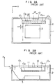
- Fig. 1 is a perspective view of a scanner portion of the supersonic flaw detecting system
- Figs. 2A and 2B are a plan view and aside view of the array probe, respectively.
- the reference numeral 1 designates a flaw-detection water tank, 2 water put into the water tank 1, and 3 an object to be inspected mounted on the bottom surface of the water tank 1.
- the reference numeral 4 generally designates a scanner portion constituted by a scanner base 5 for mounting the water tank 1 thereon, a pair of frames 6 fixed to the scanner base 5, an arm 7 disposed between the frames 6, a holder 8 disposed on the arm 7, a pole 9 attached to the holder 8, and an array probe 10.
- the pair of frames 6 can drive the arm 7 in the Y-axis direction by a mechanism not shown.
- the arm 7 can drive the holder 8 in the X-axis direction by a mechanism not shown.
- the holder 8 and the pole 9 can cooperate to drive the array probe in the Z-axis direction (the direction orthogonal to the X- and Y-axes) by a mechanism not shown.
- the array probe 10 has a configuration in which a large number of piezoelectric elements (hereinafter referred to as "array elements”) are arranged linearly in the X-axis direction. When a pulse is given to each array element, the array element emits a supersonic wave and converts the reflected supersonic wave into an electric signal proportional thereto.
- the array elements are designated by numerals 10 1 to 10 n , respectively.
- black spots represent sampling points
- YP represents a Y-axis direction sampling pitch
- XP represents an X-axis direction sampling pitch
- AP represents an array element pitch in the array elements 10 1 to 10 n .
- the reference numeral 11 designates a package for packing the array probe 10 and the like therein.
- T 1 to T 9 represent array elements arranged linearly
- D 1 to D 9 represent delay elements connected to the array elements 10 1 to 10 9
- p represents an excitation pulse received by each of the array elements T 1 to T 9 .
- Two delay elements D 1 and D 9 are established to have an equal delay period (t 19 ).
- two delay elements D 2 and D 6 , two delay elements D 3 and D 7 , and two delay elements D 4 and D 6 are established to have equal delay periods (t 28 ), (t 37 ), and (t 46 ), respectively.
- the delay period of the delay element D 5 is represented by t 5
- the delay periods thus established satisfy the following relation. t 19 ⁇ t 28 ⁇ t 37 ⁇ t 46 ⁇ t 5
- the delay periods of the delay elements D 1 to D 9 are set to predetermined values according to the relation (1) and are supplied with excitation pulses p , then supersonic waves are emitted from the array elements T 1 to T 9 corresponding to the set delay periods. Accordingly, the supersonic waves emitted from the two array elements T 1 and T 9 are earliest and the supersonic wave emitted from the array element T 5 is last. The supersonic waves thus emitted from the array elements are propagated radially, so that there occurs a point where the maximum values of amplitude of the supersonic waves coincide with each other. This point is represented by the symbol B in Fig. 3A.
- this point B is referred to as a "focal point".
- the focal point B is shifted to a focal point B' which is further off the array probe 10, as shown in the dot-and-dash line. Accordingly, the position of the focal point can be selected by adjusting the delay periods of the delay elements D 1 to D 9 as described above. In the case where this way is adapted to detection of a flaw in the object 3, the depth of flaw detection can be selected.
- Fig. 3B is a view for explaining the function of the array probe 10 as shown in Figs. 2A and 2B.
- the reference numerals 10 1 to 10 n designate array elements which are the same as in Fig. 2A.
- Delay elements not shown are connected to the array elements 10 1 to 10 n , respectively.
- a number, m , of array elements 10 1 to 10 m are selected so that supersonic waves emitted therefrom are apparently converged into a focal point B 1 in the same manner as described above by setting the delay periods suitably.
- This focal point B 1 is represented by the symbol B 1 in the Fig. 3B.
- the array elements are shifted by one so that delay periods having the same pattern as the delay periods given to the array elements 10 1 to 10 m are given to newly selected array elements 10 2 to 10 m+1 .
- the focal point thus obtained is represented by the symbol B 2 .
- the array elements are shifted one by one and, lastly, array elements 10 n-m+1 to 10 n are selected so that delay periods having the same pattern are given to the array elements, thus to obtain a focal point B n-m+1 .
- AP represents an element pitch of the probe
- SP represents a sampling pitch.
- delay periods by reference to Figs. 3A and 3B has been applied to the case where supersonic waves are transmitted from the array elements, it is a matter of course that similar delay periods are required to be given to the array elements in the case where the supersonic waves reflected from the object are received by the array elements.
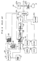
- Fig. 4 is a block diagram of the control circuit.
- the reference numeral 10 designates an array probe as described above, 7M a motor for driving the arm 7 in the Y-axis direction, 8M a motor for driving the holder 8 in the X-axis direction, 7E an encoder for generating a driving signal to be given to the motor 7M and for detecting the amount of rotations of the motor 7M, and 8E an encoder for generating a driving signal to be given to the motor 8M and for detecting the amount of rotations of the motor 8M.
- the reference numeral 20 designates a signal processor comprising a CPU (central processing unit) 20a, an image memory 20b for image processing, an interface 20c for input-output between the signal processor 20 and a certain external circuit, and a keyboard 20d.
- the signal processor 20 further has other elements such as RAM and ROM, the other elements being not shown.
- the reference numeral 21 designates a display unit.
- the reference numeral 22 designates a delay period control circuit for controlling, under orders of the CPU 20a, delay periods which have been described with reference to Figs. 3A and 3B.
- the reference numeral 23 designates pulsers for generating the excitation pulses p . In this example, a plurality of pulsers 23 are provided corresponding to the array elements.
- the reference numeral 24 designates a pulser-amplifier switching circuit for selectively switching the pulsers 23 in accordance with the instructions from the CPU 20a. The details of the pulser-amplifier switching circuit 24 will be described later.
- the reference numeral 25 designates AND circuits, and 26 amplifiers for reception and amplification of reflected wave signals of the supersonic waves emitted from the array elements.
- the AND circuits 25 and the amplifiers 26 are similarly provided corresponding to the array elements.
- the reference numeral 27 designates a delay period control circuit, and 28 a waveform adder.
- the waveform adder 28 serves to add up all reception signals obtained simultaneously as the result of delaying in the delay period control circuit 27.
- the reference numeral 29 designates a peak detector having a gate function for picking up signals in a predetermined range of depth from the surface of the object 3 and a function for storing only a peak value within the range and sending out the peak value.
- the reference numeral 30 designates an A/D converter for converting the peak value stored in the peak detector 29, into a digital value.
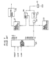
- Fig. 5 is a block diagram of the pulser-amplifier switching circuit
- Fig. 6 is a timing chart of the pulser-amplifier switching circuit.
- Figs. 5 to 6 show the case where the number of array elements to be excited at once is four. As shown in Fig.
- the pulser-amplifier switching circuit 24 is constituted by a shift register formed by series connection of R-S master-slave flip-flop circuits (hereinafter referred to merely as "flip-flop") F 1 to F n+3 in the number corresponding to the number of the array elements.
- Q 1 to Q n+3 represent output signals of the flip-flops F 1 to F n+3 .
- the pulser-amplifier switching circuit 24 operates as follows.
- the levels of the output signals Q 1 to Q 4 of the flip-flops F 1 to F 4 each in a preset state become high as shown in the diagrams (G) to (J) of Fig. 6 immediately after the preset pulses PR 1 to PR 4 are received.
- These four high-level output signals Q 1 to Q 4 serve as excitation signals for four array elements of from the first-order element to the fourth-order element.
- the excitation signals are fed to the four array elements in a first time E 1 .
- the clock pulse C 1 is received, the level of the output signal Q 1 becomes low as shown in Fig. 6(G) because the level of the S terminal of the flip-flop F 1 is low.
- Fig. 7 is a simplified block diagram of an array element excitation circuit. Like numerals in each of Figs. 4 and 7 refer to like parts. For simplification of illustration, a circuit corresponding to one array element 10 1 is shown in Fig. 7. As described above, the number of the pulsers 23, the number ((n+3) in Fig. 3) of the AND circuits 25 and the number of the amplifiers 26 are, in practice, respectively equal to the number, n , of the array elements. When instructions from the CPU 20 are given to the pulser-amplifier switching circuit 24, the level of the output signal Q 1 of the flip-flop F 1 becomes high as described above.
- the output signal Q 1 is fed to the AND circuit 25 and then taken out from the AND circuit 25 after a predetermined delay period given by the delay period control circuit 22.
- the pulser 23 On the basis of the output signal, the pulser 23 generates an excitation pulse to excite the array element 10 1 to thereby emit a supersonic wave.
- the output signal Q 1 is connected also to the amplifier 26.
- This signal serves as a trigger signal for the amplifier 26, so that the amplifier 26 operates when the level of the output signal Q 1 is high but the operation of the amplifier 26 stops when the level is low.
- the fact that the operation stops means the fact that the input signal of the amplifier 26 is not transmitted to the output side thereof.
- the reflected supersonic wave is received by the same array element 10 1 and converted into an electric signal.
- the electric signal is amplified by the amplifier 26 and delayed for a time determined by the reception delay period control circuit 27 and equal to the time determined by the transmission delay period control circuit 22. Then, the signal is fed to the waveform adder 28.
- the waveform adder 28 serves to add up (four) reception signals of simultaneously excited array elements to feed an adder signal to the image memory 20b of the signal processor 20 via the peak detector 29 and the A/D converter 30.
- the aforementioned procedure is repeated n times while array elements are successively shifted by one, so that the adder signals thus successively obtained are stored in the image memory 20b.
- one-line supersonic wave scanning in the X-axis direction by use of the array probe 10 is performed.
- the CPU 20a drives the motor 7M to move the array probe 10 by a predetermined sampling pitch (YP) in the Y-axis direction. Then, the aforementioned procedure started by application of clear pulses is repeated again to carry out supersonic scanning in the X-axis direction by use of respective array elements. As described above, X-axis direction supersonic scanning and Y-axis direction sampling pitch movement are repeated to thereby carry out flaw detection in a predetermined range of coordinates (X, Y) in a plane in the object 3. The time required for scanning one line in the X-axis direction is very short because of the electronic scanning, so that the motor in the Y-axis direction can be driven continuously.
- flaw detection data at intersections determined by the X-axis direction sampling pitch XP (for example, the distance between adjacent array elements) and the Y-axis direction sampling pitch YP are stored in the image memory 20b.
- the signal processor 20 processes the data stored in the image memory 20b so that the resulting data are displayed on the display unit 21.
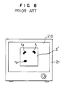
- Fig. 8 shows an example of display in the display unit.
- the reference numeral 21D designates a display surface of the display unit 21
- the reference numeral 3′ designates a supersonic image of the object 3 displayed on the display surface
- f 1 to f 3 designate flaw images in the supersonic image 3′.
- the concept "flaw” herein used includes internal separation of an IC package, corrosion of a plating layer of a steel pipe, and gross porosity of a casting.
- the display surface 21D has a large number of picture elements arranged in the form of a matrix.
- the picture elements in the display surface 21D are numbered corresponding to the addresses in the image memory 20b, so that the signal processor 20 can carry out display of the data stored in the image memory 20b.
- U.S. Patent 4,768,155 discloses a supersonic flaw detecting system in which a probe of single type, not array type, is mechanically moved both in the X-axis direction and in the Y-axis direction for the purpose of scanning.
- this supersonic flaw detecting system conducts mechanical scanning in the X-axis direction as well as in the Y-axis direction, the time required for obtaining one scene is of the order of tens of seconds.
- the first prior art type supersonic flaw detecting system as described above with reference to Figs. 1 to 8 conducts supersonic flaw detection in an X-Y plane (C- scope) in a predetermined depth from the surface of the object 3 to obtain a supersonic image in the plane, so that existence of flaws can be found.
- the second prior art type supersonic flaw detecting system is configured so that a C-scope image (horizontal sectional image) is displayed and then an A-scope image can be obtained in a desired position of the C-scope image.
- the system is so slow that the time of from the order of tens of seconds to the order of minutes is required for obtaining the C-scope image, because the scanning both in the X-direction and in the Y-direction is mechanical.
- the first prior art type system is so speedy that the time required for obtaining the C-scope image is about one second or of the order of seconds, but the system is not suitable for detailed inspection though the detailed inspection is necessary.
- a supersonic flaw detecting system comprises: an array probe constituted by a large number of array elements arranged in a direction of a first axis for serving transmission and reception of supersonic waves; switching means for switching the array elements so as to successively select a predetermined number of ones of the array elements on the basis of a clock signal; moving means for moving the array probe in a direction of a second axis orthogonal to the first axis; delay control means provided both in the transmission side and in the reception side for the double purpose of converging supersonic waves at a predetermined point and receiving reflection waves from the point; a display portion for displaying a supersonic image in a plane formed by the first and second axes on the basis of signals received by the array elements; cursor display means for displaying a cursor in the display portion; computing means for computing the amount of movement of the cursor; clock signal output control means for generating the clock signal having a number of pulses corresponding to
- the supersonic flaw detecting system comprises: an array probe constituted by a large number of array elements arranged both in a direction of a first axis and in a direction of a second axis orthogonal thereto for serving transmission and reception of supersonic waves; switching means for switching the array elements so as to successively select a predetermined number of ones of the array elements on the basis of a clock signal; delay control means provided both in the transmission side and in the reception side for the double purpose of converging supersonic wave at a predetermined point and receiving reflection waves from the point; a display portion for displaying a supersonic image in a plane formed by the first and second axes on the basis of signals received by the array elements; cursor display means for displaying a cursor in the display portion; computing means for computing the amounts of movement of the cursor in the first and second axial directions; clock signal output control means for generating the clock signal having a number of pulses corresponding to the amount of movement
- a cursor can be displayed in the display portion and can be quickly moved to the desired position.
- the distances of the movement in the first and second-axis directions which form the plane are computed by the computing means.
- the array probe is constituted by array elements arranged in the first-axis direction
- a number of clock pulses corresponding to the distance of the first-axis direction movement of the cursor are generated and, at the same time, the array probe is moved in the second-axis direction by a distance corresponding to the distance of the second-axis direction movement of the cursor.
- the array probe is constituted by array elements arranged in the form of a matrix in the first and second-axis directions
- a number of clock pulses corresponding to the distance of the first-axis direction movement of the cursor and a number of clock pulses corresponding to the distance of the second-axis direction movement of the cursor are given to the first and second-axis directions of the array elements.
- a supersonic image in a direction of an axis orthogonal to the first and second axes can be obtained in the desired position of the object corresponding to the position of the cursor, so that more detailed analysis can be made on the basis of the supersonic image.
- a detecting system is known from US-A-4 664 122.
- This medical diagnostic system generates a B-scope image of a patient's body and allows the user to select a point in this B-scope image, at which a tissue velocity or a blood flow rate is measured and is displayed simultaneously with the B-scope image.
- This system does not convey an idea of the three-dimensional nature of an inspected object, either.
- FIGs. 1 to 8 A prior art type supersonic flaw detecting system is shown in Figs. 1 to 8, in which:
- Figs. 9 to 12 show a supersonic flaw detecting system according to the third example.
- Fig. 9 is a block diagram of a control circuit in a supersonic flaw detecting system.
- items the same as or equivalent to those in Fig. 4 are referenced correspondingly.
- the reference numeral 20a' designates a CPU similar to the CPU 20a but different from the latter in processing contents.
- the reference numeral 20d' designates a keyboard similar to the keyboard 20d but different from the latter in that the keyboard 20d' includes cursor operation keys.
- the cursor operation keys include seven keys, that is, a cursor up key ( ⁇ ), a cursor down key ( ⁇ ), a cursor left key ( ⁇ ), a cursor right key ( ⁇ ), a cursor stop key (S), a key (B) used when the cursor is moved from the current position, and a cursor function program stop key (R).
- the reference numeral 20' designates a signal processor constituted by a CPU 20a', an image memory 20b, an interface 20c and a keyboard 20d'.
- the reference numeral 21′ designates a display unit similar to the display unit 21.
- the display unit 21′ will be described later.
- the reference numeral 31 designates an oscilloscope for displaying an output signal of the waveform adder 28.
- the arrangement of parts in Fig. 9 is the same as that of parts in Fig. 4, except the signal processor 20′, the display unit 21′ and the oscilloscope 31.
- Fig. 10 is a view showing the display surface of the display unit shown in Fig. 9.
- the reference numeral 21′ designates a display unit, and 21D′ a display surface thereof.
- C represents a cursor displayed on the display surface 21D′.
- the display unit 21′ is different from the display unit 21 in that the display unit 21′ has means for displaying the cursor C.
- cursor display control is carried out by the CPU 20a′, the display unit 21′ can be replaced by the display unit 21.
- the cursor C is displayed in a supersonic scanning start point (X 1 , Y 1 ).
- the cursor C can be moved vertically and horizontally on the basis of cursor operation keys (not shown) in the keyboard 20d′.
- address setting is carried out so that addresses X a and Y a in the movement start time are X aa and Y aa , respectively (the step S 2 ).
- a cursor C is displayed in a postion (X a , Y a ) of the display surface 21D′ corresponding to the addresses X a and Y a (the step S 3 ).
- the cursor C is moved to a desired position, for example, position (X v , Y w ) in Fig.
- the movement is made by shifting the cursor C by one picture element (one address) according to the movement instruction direction of the operation key, judging which of four cursor operation keys instructing to move the cursor up, down, left and right is operated in the keyboard 20d′.
- the cursor C is moved by (V-1) in the X-axis direction and by (W-1) in the Y-axis direction.
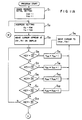
- a judgment is made as to whether the cursor stop key S is operated or not. when the position of the cursor C is decided, the procedure is shifted to the step S 14 in Fig. 11B.
- step S 14 how much the array probe 10 must be moved in the Y-axis direction is computed.
- Y m is calculated by multiplying the Y-axis direction sampling pitch YP by a value obtained by subtracting the movement start-time address Y a from the current Y-axis direction address Y aa .
- the CPU 20a′ drives the motor 7M to move the array probe 10 by Y m in the Y-axis direction (the step S 15 ).
- the aforementioned procedure is a procedure for moving a supersonic beam to the Y-axis direction position Y w .
- the procedure for moving a supersonic beam to the X-axis direction position X v is described.
- the supersonic beam can be moved in the X-axis direction by one array element pitch (sampling pitch XP) whenever one clock pulse is given to the shift register (composed of flip-flops) forming the pulser-amplifier switching circuit 24.
- clear pulses are given to the shift register as described above (the step S 16 ) and then preset pulses are given to simultaneously excited array elements (the step S 16 ).
- clock pulses are given, the supersonic beam is successively shifted in the X-axis direction for every clock pulse.
- the clock pulse is given at (X aa -1) times (the step S 18 ).
- the output state of the shift register and the X-axis direction position of the supersonic beam when the clock pulse is given at (X aa -1) times are explained by reference to Table.
- the number of simultaneously excited array elements is four as shown in Fig. 5 and the position of X-axis direction movement of the cursor C is position X y as shown in Fig. 10.
- the levels of the output signals Q 1 to Q 4 become high to excite the first four array elements.
- the X-direction convergent position of the supersonic beam is made to coincide with the position X 1 .
- the levels of the output signals Q 2 to Q 5 of the shift register become high, so that simultaneously excited array elements are shifted by one in the X-axis direction and, accordingly, the convergent position of the supersonic beam is shifted by one array element pitch, that is, one sampling pitch XP. Accordingly, the convergent position of the supersonic beam becomes the position X 2 .
- This operation is repeated.
- the levels of the output signals Q v to Q v+3 become high and, accordingly, the convergent position of the supersonic beam becomes the position X v .
- the supersonic beam is radiated to the position (X v , Y w ).
- the reflected wave of the supersonic beam is received by excited array elements and then sent out from the waveform adder 28 as described above.
- the oscilloscope 31 is operated on the basis of the output signal of the waveform adder 28 to display the waveform of the signal.
- the waveform (A-scope image) is a Z-axis direction supersonic flaw detection waveform in the position (X v , Y w ), by which more detailed flaw detection in the position is carried out.
- the CPU 20a′ judges the state of the cursor operation key B in the keyboard 20d′ (the step S 20 ).
- the state of the cursor operation key R is judged (the step S 21 ).
- the procedure is returned to the step S 19 so that a supersonic beam is repeatedly radiated to the position (X v , Y w ) and then the reflected waveform is displayed on the oscilloscope 31.
- the cursor operation key B is judged to be operative, the procedure is returned to the step S 2 so that the movement of the cursor C is carried out again.
- the addresses X aa and Y aa correspond to the movement start position.
- a cursor is displayed and moved to a desired position of the supersonic image obtained by supersonic scanning of a plane of the object by use of a probe array and is moved to a desired position of the supersonic image, so that a supersonic wave is emitted to a position of the object corresponding to the position and then the reflected signal is observed by the oscilloscope. Accordingly, not only supersonic flaw detection on a plane of the object can be conducted but also supersonic flaw detection in the depth in the desired position of the object can be conducted. Consequently, more detailed analysis of a flaw portion can be made.
- the same principle of operation can be applied to the case where the probe has also the probe array in the Y-axis direction, that is, the probe has array elements arranged in the form of a matrix.
- the focal position of the supersonic beam in the cursor position is constant but when more detailed information in the direction of depth is required, the focal depth can be changed by changing the delay period variously.
- FIG. 13-16 An embodiment of the invention is now described referring to Figs 13-16. It is capable of displaying a plane image (C-scope) and a sectional image (B-scope) at once.
- a plane image (C-scope image) 40 is displayed on a monitor TV 37 as a display unit in the same manner as in the prior art. Then, a line cursor 41 is presented in parallel to the X-axis direction and moved in the Y-direction by operation of the keyboard 20D.
- B-scope image a detailed sectional image (B-scope image) 42 in a portion (shown by the line cursor 41) crossing two flaws F1 and F2 as shown in Fig. 13
- the B-scope image 42 in the line cursor position can be observed under the plane image (C-scope image) 41 as shown in Fig. 13 by pushing a keyboard input key such as return key "RET" while setting the line cursor 41 in the shown position.
- the array probe 10 is mechanically moved to the position of the line cursor 41 by the motor.
- electronic scanning in this case, linear scanning
- B-scope display B-scope display
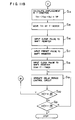
- a block diagram of the system in this embodiment is shown in Fig. 14. Double-framed blocks are newly provided.
- a switching circuit 35 following the waveform adder 28 serves to switch between B-scope display and C-scope display.
- the switching circuit 35 serves to switch electronically alternately therebetween in a time of the order of msec.
- B-scope display is selected.
- C-scope display is selected.
- the output signal thereof passes through a detector circuit 38.
- the waveform of the input signal of the detector circuit 38 is Rf waveform Rf as shown in the diagram (A) of Fig. 15.
- the signal is full-wave rectified by the detector circuit 38 to obtain a full-wave rectified waveform FR as shown in the diagram (B) of Fig. 15 and then obtain an envelope waveform EW as shown in the diagram (C) of Fig. 15.
- the output waveform (in the diagram (C) of Fig. 15) of the detector circuit is digitalized at a predetermined sampling interval as shown in the view (D) of Fig. 15.
- sampling may be applied to the Rf waveform in the diagram (A) of Fig. 15.
- the A/D conversion is, in practice, not speedy enough to trace the up and down movement of the Rf waveform. Accordingly, the frequency of the waveform is reduced by the detector circuit.
- the next subject is how to feed, as a B-scope image 42, the A/D converted data to the monitor TV 37.
- a method which has been developed and has been put into practical use for supersonic diagnosing apparatus and the like in a medical field is used herein.
- the method is called digital scan converter (hereinafter abbreviated to "DSC").
- the function of the DSC is to convert a supersonic image according to any one of various scanning methods into an image according to a standard TV scanning method to thereby display the image on a TV monitor.
- This function is attained by the steps of: digitalizing supersonic echo by use of the A/D converter 45; writing the digital signal in a frame memory 36 in accordance with a supersonic scanning method (In this embodiment, the method is called "linear scan”. Other scanning methods include "sector scan” and the like.); and reading the data from the frame memory 36 in accordance with a TV scanning method. (The data are converted into analog data by D/A conversion when the data are read out.)
- a C-scope image can be obtained by applying a gate signal G from the gate circuit 50 to the Rf waveform RF as shown in the Diagrams (A) and (B) of Fig. 16.
- the gate circuit 50 has polarity switching-over means for selecting one from the two of positive (+) and negative (-).
- positive (+) an analog (direct-current) voltage proportional to the maximum value (V p ) of the positive side of the waveform in the gate is generated.
- negative (-) an analog (direct-current) voltage proportional to the maximum value (V N ) of the negative side thereof is generated.
- the analog output is converted into a digital signal at every sampling pitch to thereby be transmitted to a predetermined address in the frame memory 36.
- switching means such as a switching circuit is provided so that a B-scope image can be formed in a desired position after a C-scope image is formed. Because the C-scope image (horizontal sectional image) and the B-scope image (vertical sectional image) can be displayed at once, more detailed inspection can be made. Further, because the position of B-scope display is very exact, the real position of the flaw in the object can be found exactly.
- a cursor can be displayed on a screen of display of a supersonic image obtained by scanning the surface of an object to be inspected by use of a probe formed by arrangement of array elements and, further, the cursor can be moved to a desired position of the supersonic image so that supersonic waves are emitted to a position of the surface of the object corresponding to the aforementioned position and the reflected wave signals are displayed in another display portion.
- C-scope supersonic flaw detection
- A-scope and B-scope supersonic flaw detection in the direction of depth in a desired position of the object can be conducted. Consequently, detailed analysis of the flaw portion can be made.
Description
- The present invention relates to a supersonic flaw detecting system for detecting flaws in an object to be inspected by use of a supersonic wave, and, more particularly, relates to a supersonic flaw detecting system which is suitable for detecting, in detail and quickly, internal flaw conditions of an object to be examined.
- A supersonic flaw detecting system has been used in various fields for the purpose of detecting internal flaws of an object to be inspected without destruction. In most cases, existence of internal flaws of an object to be inspected is checked within a predetermined range of the object. In such cases, the aforementioned range of the surface of the object is scanned by a probe to conduct flaw detection. As the probe, an array probe constituted by a large number of piezoelectric elements arranged linearly has been put into practical use, for example, as described in the paper by J. Kubota et al., entitled "High Speed Ultrasonic Image of IC Package". A supersonic flaw detecting system using such an array probe will be described hereunder.
- Fig. 1 is a perspective view of a scanner portion of the supersonic flaw detecting system, and Figs. 2A and 2B are a plan view and aside view of the array probe, respectively. In the drawings, the
reference numeral 1 designates a flaw-detection water tank, 2 water put into thewater tank water tank 1. Thereference numeral 4 generally designates a scanner portion constituted by ascanner base 5 for mounting thewater tank 1 thereon, a pair offrames 6 fixed to thescanner base 5, anarm 7 disposed between theframes 6, aholder 8 disposed on thearm 7, apole 9 attached to theholder 8, and anarray probe 10. The pair offrames 6 can drive thearm 7 in the Y-axis direction by a mechanism not shown. Thearm 7 can drive theholder 8 in the X-axis direction by a mechanism not shown. Theholder 8 and thepole 9 can cooperate to drive the array probe in the Z-axis direction (the direction orthogonal to the X- and Y-axes) by a mechanism not shown. - The
array probe 10 has a configuration in which a large number of piezoelectric elements (hereinafter referred to as "array elements") are arranged linearly in the X-axis direction. When a pulse is given to each array element, the array element emits a supersonic wave and converts the reflected supersonic wave into an electric signal proportional thereto. In Figs. 2A and 2B, the array elements are designated bynumerals 101 to 10n, respectively. In the drawings, black spots represent sampling points, YP represents a Y-axis direction sampling pitch, XP represents an X-axis direction sampling pitch, and AP represents an array element pitch in thearray elements 101 to 10n. The reference numeral 11 designates a package for packing thearray probe 10 and the like therein. - The outline of the function of the
array probe 10 will be described with reference to Figs. 3A and 3B. In Fig. 3A, T1 to T9 represent array elements arranged linearly, D1 to D9 represent delay elements connected to thearray elements 101 to 109, and p represents an excitation pulse received by each of the array elements T1 to T9. Two delay elements D1 and D9 are established to have an equal delay period (t19). Similarly, two delay elements D2 and D6, two delay elements D3 and D7, and two delay elements D4 and D6 are established to have equal delay periods (t28), (t37), and (t46), respectively. When the delay period of the delay element D5 is represented by t5, the delay periods thus established satisfy the following relation.
- Assuming now that the delay periods of the delay elements D1 to D9 are set to predetermined values according to the relation (1) and are supplied with excitation pulses p, then supersonic waves are emitted from the array elements T1 to T9 corresponding to the set delay periods. Accordingly, the supersonic waves emitted from the two array elements T1 and T9 are earliest and the supersonic wave emitted from the array element T5 is last. The supersonic waves thus emitted from the array elements are propagated radially, so that there occurs a point where the maximum values of amplitude of the supersonic waves coincide with each other. This point is represented by the symbol B in Fig. 3A. Because the magnitude of the supersonic wave at this point B is far larger than the magnitude of the supersonic wave at another point, the supersonic waves emitted from the array elements T1 to T9 are in such a state that they are converged into the point B as shown in the broken line. In other words, if suitable delay periods are given to the supersonic waves emitted from the array elements arranged linearly, an effect that the supersonic waves are converged into the point B can be attained. Hereinafter, this point B is referred to as a "focal point". If the delay periods are set to be respectively smaller than the aforementioned delay periods while the relation (1) is satisfied, the focal point B is shifted to a focal point B' which is further off the
array probe 10, as shown in the dot-and-dash line. Accordingly, the position of the focal point can be selected by adjusting the delay periods of the delay elements D1 to D9 as described above. In the case where this way is adapted to detection of a flaw in theobject 3, the depth of flaw detection can be selected. - Fig. 3B is a view for explaining the function of the
array probe 10 as shown in Figs. 2A and 2B. In the drawing, thereference numerals 101 to 10n designate array elements which are the same as in Fig. 2A. Delay elements not shown are connected to thearray elements 101 to 10n, respectively. In the example of Fig. 3B, a number, m, ofarray elements 101 to 10m are selected so that supersonic waves emitted therefrom are apparently converged into a focal point B1 in the same manner as described above by setting the delay periods suitably. This focal point B1 is represented by the symbol B1 in the Fig. 3B. Then, the array elements are shifted by one so that delay periods having the same pattern as the delay periods given to thearray elements 101 to 10m are given to newly selectedarray elements 102 to 10m+1. The focal point thus obtained is represented by the symbol B2. Similarly, the array elements are shifted one by one and, lastly,array elements 10n-m+1 to 10n are selected so that delay periods having the same pattern are given to the array elements, thus to obtain a focal point Bn-m+1. By the aforementioned procedure, flaw-detection scanning from the focal point B1 to the focal point Bn-m+1 by thearray probe 10 can be conducted consequently. In Fig. 3B, AP represents an element pitch of the probe, and SP represents a sampling pitch. Although Fig. 3B shows the case where AP is equal to SP, the values of AP and SP may be established by use of known electronic control means to satisfy the equation SP=(1/2)AP or SP=(1/4)AP. - Although the description of delay periods by reference to Figs. 3A and 3B has been applied to the case where supersonic waves are transmitted from the array elements, it is a matter of course that similar delay periods are required to be given to the array elements in the case where the supersonic waves reflected from the object are received by the array elements.
- In the following, a control circuit in the supersonic flaw detecting system using the array probe is described. Fig. 4 is a block diagram of the control circuit. In Fig. 4 the
reference numeral 10 designates an array probe as described above, 7M a motor for driving thearm 7 in the Y-axis direction, 8M a motor for driving theholder 8 in the X-axis direction, 7E an encoder for generating a driving signal to be given to themotor 7M and for detecting the amount of rotations of themotor motor 8M and for detecting the amount of rotations of themotor 8M. Thereference numeral 20 designates a signal processor comprising a CPU (central processing unit) 20a, animage memory 20b for image processing, aninterface 20c for input-output between thesignal processor 20 and a certain external circuit, and akeyboard 20d. Thesignal processor 20 further has other elements such as RAM and ROM, the other elements being not shown. Thereference numeral 21 designates a display unit. - The
reference numeral 22 designates a delay period control circuit for controlling, under orders of theCPU 20a, delay periods which have been described with reference to Figs. 3A and 3B. Thereference numeral 23 designates pulsers for generating the excitation pulses p. In this example, a plurality ofpulsers 23 are provided corresponding to the array elements. Thereference numeral 24 designates a pulser-amplifier switching circuit for selectively switching thepulsers 23 in accordance with the instructions from theCPU 20a. The details of the pulser-amplifier switching circuit 24 will be described later. Thereference numeral 25 designates AND circuits, and 26 amplifiers for reception and amplification of reflected wave signals of the supersonic waves emitted from the array elements. The ANDcircuits 25 and theamplifiers 26 are similarly provided corresponding to the array elements. Thereference numeral 27 designates a delay period control circuit, and 28 a waveform adder. Thewaveform adder 28 serves to add up all reception signals obtained simultaneously as the result of delaying in the delayperiod control circuit 27. Thereference numeral 29 designates a peak detector having a gate function for picking up signals in a predetermined range of depth from the surface of theobject 3 and a function for storing only a peak value within the range and sending out the peak value. Thereference numeral 30 designates an A/D converter for converting the peak value stored in thepeak detector 29, into a digital value. - The configuration and operation of the pulser-
amplifier switching circuit 24 will be now described with reference to Fig. 5 and Fig. 6 (diagrams (A) through (O)). Fig. 5 is a block diagram of the pulser-amplifier switching circuit, and Fig. 6 (diagrams (A) through (O)) is a timing chart of the pulser-amplifier switching circuit. For simplification of illustration, Figs. 5 to 6 show the case where the number of array elements to be excited at once is four. As shown in Fig. 5, the pulser-amplifier switching circuit 24 is constituted by a shift register formed by series connection of R-S master-slave flip-flop circuits (hereinafter referred to merely as "flip-flop") F1 to Fn+3 in the number corresponding to the number of the array elements. In the drawing, Q1 to Qn+3 represent output signals of the flip-flops F1 to Fn+3. The pulser-amplifier switching circuit 24 operates as follows. - As shown in the diagram (B) of Fig. 6, clear pulses are fed to the CLR terminals of the flip-flops F1 to Fn+3, so that the levels of all the output signals Q1 to Qn+3 become low. Then, as shown in the diagrams (C) to (F) of Fig. 6, preset pulses PR1 to PR4 are fed to the PR terminals of first four flip-flops F1 to F4. In this condition, clock pulses C1, C2, ... as shown in the diagram (A) of Fig. 6A are fed from a clock generator (not shown) to the CK terminals of the flip-flops F1 to Fn+3, successively.
- Then, the levels of the output signals Q1 to Q4 of the flip-flops F1 to F4 each in a preset state become high as shown in the diagrams (G) to (J) of Fig. 6 immediately after the preset pulses PR1 to PR4 are received. These four high-level output signals Q1 to Q4 serve as excitation signals for four array elements of from the first-order element to the fourth-order element. The excitation signals are fed to the four array elements in a first time E1. Then, when the clock pulse C1 is received, the level of the output signal Q1 becomes low as shown in Fig. 6(G) because the level of the S terminal of the flip-flop F1 is low. At the same time, the level of the S terminal of the flip-flop F5 becomes high on the basis of the output signal Q4, so that the level of the output signal Q5 thereof becomes high as shown in the diagram (K) of Fig. 6. Accordingly, excitation signals are fed to four array elements of from the second-order array element to the fifth-order array element in a next time E2. When the next clock pulse C3 is received, the levels of the output signals Q3 to Q6 become high in a time E3 in the same manner as described above. Thus, high-level output signals are successively shifted one by one, so that the array elements are successively selected by fours.
- In the following, the operation of the pulser-
amplifier switching circuit 24 shown in Fig. 4 is described with reference to Fig. 7. Fig. 7 is a simplified block diagram of an array element excitation circuit. Like numerals in each of Figs. 4 and 7 refer to like parts. For simplification of illustration, a circuit corresponding to onearray element 101 is shown in Fig. 7. As described above, the number of thepulsers 23, the number ((n+3) in Fig. 3) of the ANDcircuits 25 and the number of theamplifiers 26 are, in practice, respectively equal to the number, n, of the array elements. When instructions from theCPU 20 are given to the pulser-amplifier switching circuit 24, the level of the output signal Q1 of the flip-flop F1 becomes high as described above. The output signal Q1 is fed to the ANDcircuit 25 and then taken out from the ANDcircuit 25 after a predetermined delay period given by the delayperiod control circuit 22. On the basis of the output signal, thepulser 23 generates an excitation pulse to excite thearray element 101 to thereby emit a supersonic wave. Further, the output signal Q1 is connected also to theamplifier 26. This signal serves as a trigger signal for theamplifier 26, so that theamplifier 26 operates when the level of the output signal Q1 is high but the operation of theamplifier 26 stops when the level is low. The fact that the operation stops means the fact that the input signal of theamplifier 26 is not transmitted to the output side thereof. The reflected supersonic wave is received by thesame array element 101 and converted into an electric signal. The electric signal is amplified by theamplifier 26 and delayed for a time determined by the reception delayperiod control circuit 27 and equal to the time determined by the transmission delayperiod control circuit 22. Then, the signal is fed to thewaveform adder 28. Thewaveform adder 28 serves to add up (four) reception signals of simultaneously excited array elements to feed an adder signal to theimage memory 20b of thesignal processor 20 via thepeak detector 29 and the A/D converter 30. The aforementioned procedure is repeated n times while array elements are successively shifted by one, so that the adder signals thus successively obtained are stored in theimage memory 20b. By the n times procedures, one-line supersonic wave scanning in the X-axis direction by use of thearray probe 10 is performed. Then, theCPU 20a drives themotor 7M to move thearray probe 10 by a predetermined sampling pitch (YP) in the Y-axis direction. Then, the aforementioned procedure started by application of clear pulses is repeated again to carry out supersonic scanning in the X-axis direction by use of respective array elements. As described above, X-axis direction supersonic scanning and Y-axis direction sampling pitch movement are repeated to thereby carry out flaw detection in a predetermined range of coordinates (X, Y) in a plane in theobject 3. The time required for scanning one line in the X-axis direction is very short because of the electronic scanning, so that the motor in the Y-axis direction can be driven continuously. - Through the aforementioned operation, flaw detection data at intersections determined by the X-axis direction sampling pitch XP (for example, the distance between adjacent array elements) and the Y-axis direction sampling pitch YP are stored in the
image memory 20b. Thesignal processor 20 processes the data stored in theimage memory 20b so that the resulting data are displayed on thedisplay unit 21. Fig. 8 shows an example of display in the display unit. In the drawing, the reference numeral 21D designates a display surface of thedisplay unit 21, thereference numeral 3′ designates a supersonic image of theobject 3 displayed on the display surface, and f1 to f3 designate flaw images in thesupersonic image 3′. The concept "flaw" herein used includes internal separation of an IC package, corrosion of a plating layer of a steel pipe, and gross porosity of a casting. The display surface 21D has a large number of picture elements arranged in the form of a matrix. The picture elements in the display surface 21D are numbered corresponding to the addresses in theimage memory 20b, so that thesignal processor 20 can carry out display of the data stored in theimage memory 20b. - On the other hand, U.S. Patent 4,768,155, a prior art reference, discloses a supersonic flaw detecting system in which a probe of single type, not array type, is mechanically moved both in the X-axis direction and in the Y-axis direction for the purpose of scanning.
- Because this supersonic flaw detecting system conducts mechanical scanning in the X-axis direction as well as in the Y-axis direction, the time required for obtaining one scene is of the order of tens of seconds.
- The first prior art type supersonic flaw detecting system as described above with reference to Figs. 1 to 8 conducts supersonic flaw detection in an X-Y plane (C- scope) in a predetermined depth from the surface of the
object 3 to obtain a supersonic image in the plane, so that existence of flaws can be found. - To perform more excellent production control and quality control, detailed data of flaw such as position of a flaw depth, a flaw shape and the like are required. To obtain the information, both an A-scope image (waveform) and a B-scope image (vertical sectional image) in the position of a flaw are required. The second prior art type supersonic flaw detecting system is configured so that a C-scope image (horizontal sectional image) is displayed and then an A-scope image can be obtained in a desired position of the C-scope image. However, the system is so slow that the time of from the order of tens of seconds to the order of minutes is required for obtaining the C-scope image, because the scanning both in the X-direction and in the Y-direction is mechanical. On the contrary, the first prior art type system is so speedy that the time required for obtaining the C-scope image is about one second or of the order of seconds, but the system is not suitable for detailed inspection though the detailed inspection is necessary.
- According to a third example, which does not fall within the scope of the claims, a supersonic flaw detecting system comprises: an array probe constituted by a large number of array elements arranged in a direction of a first axis for serving transmission and reception of supersonic waves; switching means for switching the array elements so as to successively select a predetermined number of ones of the array elements on the basis of a clock signal; moving means for moving the array probe in a direction of a second axis orthogonal to the first axis; delay control means provided both in the transmission side and in the reception side for the double purpose of converging supersonic waves at a predetermined point and receiving reflection waves from the point; a display portion for displaying a supersonic image in a plane formed by the first and second axes on the basis of signals received by the array elements; cursor display means for displaying a cursor in the display portion; computing means for computing the amount of movement of the cursor; clock signal output control means for generating the clock signal having a number of pulses corresponding to the amount of movement of the cursor in the first axial direction; driving means for driving the moving means corresponding to the amount of movement of the cursor in the second axial direction; and a second display portion for displaying a supersonic image in a direction of a third axis orthogonal to the first and second axes, so that the system is capable of simultaneously conducting plane-image display (C-scope display) and waveform display (A-scope display).
- According a fourth example, which does not fall within the scope of the claims, the supersonic flaw detecting system comprises: an array probe constituted by a large number of array elements arranged both in a direction of a first axis and in a direction of a second axis orthogonal thereto for serving transmission and reception of supersonic waves; switching means for switching the array elements so as to successively select a predetermined number of ones of the array elements on the basis of a clock signal; delay control means provided both in the transmission side and in the reception side for the double purpose of converging supersonic wave at a predetermined point and receiving reflection waves from the point; a display portion for displaying a supersonic image in a plane formed by the first and second axes on the basis of signals received by the array elements; cursor display means for displaying a cursor in the display portion; computing means for computing the amounts of movement of the cursor in the first and second axial directions; clock signal output control means for generating the clock signal having a number of pulses corresponding to the amount of movement of the cursor in the first axial direction and for generating the clock signal having a number of pulses corresponding to the amount of movement of the cursor in the second axial direction; and a second display portion for displaying a supersonic image in a direction of a third axis orthogonal to the first and second axes, so that the system is capable of simultaneously conducting plane-image display (C-scope display) and waveform display (A-scope display).
- When a plane supersonic image is obtained in the display portion and then more detailed analysis in a desired position of the supersonic image is required, a cursor can be displayed in the display portion and can be quickly moved to the desired position. With the movement of the cursor, the distances of the movement in the first and second-axis directions which form the plane are computed by the computing means. In the case where the array probe is constituted by array elements arranged in the first-axis direction, a number of clock pulses corresponding to the distance of the first-axis direction movement of the cursor are generated and, at the same time, the array probe is moved in the second-axis direction by a distance corresponding to the distance of the second-axis direction movement of the cursor. In the case where the array probe is constituted by array elements arranged in the form of a matrix in the first and second-axis directions, a number of clock pulses corresponding to the distance of the first-axis direction movement of the cursor and a number of clock pulses corresponding to the distance of the second-axis direction movement of the cursor are given to the first and second-axis directions of the array elements. Accordingly, in any case, supersonic waves converged into the desired position in the plane, of the object corresponding to the position of the cursor is emitted. Reflected wave of the supersonic wave is received and displayed in the other display portion having a time axis. Accordingly, a supersonic image in a direction of an axis orthogonal to the first and second axes can be obtained in the desired position of the object corresponding to the position of the cursor, so that more detailed analysis can be made on the basis of the supersonic image.
- However, it is still difficult for a user to obtain an idea of the three-dimensional shape and type of a flaw from C- and A-scope images alone.
- A detecting system according to the preamble of
claim 1 is known from US-A-4 664 122. This medical diagnostic system generates a B-scope image of a patient's body and allows the user to select a point in this B-scope image, at which a tissue velocity or a blood flow rate is measured and is displayed simultaneously with the B-scope image. This system does not convey an idea of the three-dimensional nature of an inspected object, either. - It is therefore the object of the present invention to provide a supersonic flaw detecting system by which a flaw can be readily and quickly detected and inspected in three dimensions.
- This object is achieved by a supersonic flaw detecting system according to
claim 1. Dependent claims relate to advantageous embodiments of the invention. - A prior art type supersonic flaw detecting system is shown in Figs. 1 to 8, in which:
- Fig. 1 is a perspective view of a scanner portion of the supersonic flaw detecting system;
- Figs. 2A and 2B are a plan view and a side view of an array probe;
- Figs. 3A and 3B are views for explaining the focusing function of the array probe;
- Fig. 4 is a block diagram showing an example of electric circuit configuration of the prior art type supersonic flaw detecting system;
- Fig. 5 is a block diagram showing in detail the pulser-amplifier switching circuit depicted in Fig. 4;
- Fig. 6 (including diagrams (A) to (O)) is a timing chart for explaining the operation of the pulser-amplifier switching circuit;
- Fig. 7 is a block diagram showing in detail a part of the circuit depicted in Fig. 4; and
- Fig. 8 is a front view showing the display plane of the display unit depicted in Fig. 4.
- Fig. 9 is an electric circuit block diagram of a supersonic flaw detecting system according to the third example;
- Fig. 10 is a front view showing the display plane of the display unit depicted in Fig. 9;
- Figs. 11A and 11B are flow charts for explaining the operation of the system depicted in Fig. 9; and
- Fig. 12 (including diagrams (A) to (L)) is a timing chart for explaining the operation of the system depicted in Fig. 9.
- An embodiment of the invention is shown in Figs. 13 to 16, in which:
- Fig. 13 is a front view showing the display plane of a TV monitor;
- Fig. 14 is an electric circuit block diagram similar to Fig. 4;
- Fig. 15 shows signal-processed waveforms (A) to (D) for forming a sectional-image (B-scope image) of an object to be inspected; and
- Fig. 16 shows signal-processed waveforms (A) and (B) for forming a plane image (C-scope image) of the object.
- Figs. 9 to 12 show a supersonic flaw detecting system according to the third example.
- Fig. 9 is a block diagram of a control circuit in a supersonic flaw detecting system. In Fig. 9, items the same as or equivalent to those in Fig. 4 are referenced correspondingly. In Fig. 9, the
reference numeral 20a' designates a CPU similar to theCPU 20a but different from the latter in processing contents. Thereference numeral 20d' designates a keyboard similar to thekeyboard 20d but different from the latter in that thekeyboard 20d' includes cursor operation keys. The cursor operation keys include seven keys, that is, a cursor up key (↑), a cursor down key (↓), a cursor left key (←), a cursor right key (→), a cursor stop key (S), a key (B) used when the cursor is moved from the current position, and a cursor function program stop key (R). The reference numeral 20' designates a signal processor constituted by aCPU 20a', animage memory 20b, aninterface 20c and akeyboard 20d'. Thereference numeral 21′ designates a display unit similar to thedisplay unit 21. Thedisplay unit 21′ will be described later. Thereference numeral 31 designates an oscilloscope for displaying an output signal of thewaveform adder 28. The arrangement of parts in Fig. 9 is the same as that of parts in Fig. 4, except thesignal processor 20′, thedisplay unit 21′ and theoscilloscope 31. - Fig. 10 is a view showing the display surface of the display unit shown in Fig. 9. In Fig. 10, items the same as or equivalent to those in Fig. 8 are referenced correspondingly. In Fig. 10, the
reference numeral 21′ designates a display unit, and 21D′ a display surface thereof. In Fig. 10, C represents a cursor displayed on the display surface 21D′. Thedisplay unit 21′ is different from thedisplay unit 21 in that thedisplay unit 21′ has means for displaying the cursor C. In the case where cursor display control is carried out by theCPU 20a′, thedisplay unit 21′ can be replaced by thedisplay unit 21. The cursor C is displayed in a supersonic scanning start point (X1, Y1). The cursor C can be moved vertically and horizontally on the basis of cursor operation keys (not shown) in thekeyboard 20d′. - In the following, the operation of this embodiment is described with reference to the flow charts of Figs. 11A and 11B and the timing charts of Fig. 12 including the diagrams (A) to (L). First, the
CPU 20a′ initializes theimage memory 20b (the step S1 in Fig. 11A). In other words, addresses Xaa and Yaa corresponding to the supersonic flaw detection start point in the X-axis direction address Xa and the Y-axis direction address Ya in theimage memory 20b are initialized. In this case, Xaa=1 and Yaa=1. Then, address setting is carried out so that addresses Xa and Ya in the movement start time are Xaa and Yaa, respectively (the step S2). Then, a cursor C is displayed in a postion (Xa, Ya) of the display surface 21D′ corresponding to the addresses Xa and Ya (the step S3). In this case, Xaa=1 and Yaa=1, so that the cursor C is displayed in the supersonic flaw detection start position (X1, Y1) as shown in Fig. 10. Thereafter, the cursor C is moved to a desired position, for example, position (Xv, Yw) in Fig. 2, by the steps S4 to S13. The movement is made by shifting the cursor C by one picture element (one address) according to the movement instruction direction of the operation key, judging which of four cursor operation keys instructing to move the cursor up, down, left and right is operated in thekeyboard 20d′. In the case of Fig. 10, the cursor C is moved by (V-1) in the X-axis direction and by (W-1) in the Y-axis direction. In the step S13, a judgment is made as to whether the cursor stop key S is operated or not. when the position of the cursor C is decided, the procedure is shifted to the step S14 in Fig. 11B. - In the step S14, how much the
array probe 10 must be moved in the Y-axis direction is computed. When the distance of movement is represented by Ym, Ym is calculated by multiplying the Y-axis direction sampling pitch YP by a value obtained by subtracting the movement start-time address Ya from the current Y-axis direction address Yaa. In the case of Fig. 10, Yaa=W and Ya=1. Accordingly, the distance Ym of the Y-axis direction movement of the cursor C is represented by the equation Ym=(W-1)·YP. TheCPU 20a′ drives themotor 7M to move thearray probe 10 by Ym in the Y-axis direction (the step S15). In short, the aforementioned procedure is a procedure for moving a supersonic beam to the Y-axis direction position Yw. - In the following, the procedure for moving a supersonic beam to the X-axis direction position Xv is described. As described above, the supersonic beam can be moved in the X-axis direction by one array element pitch (sampling pitch XP) whenever one clock pulse is given to the shift register (composed of flip-flops) forming the pulser-
amplifier switching circuit 24. Now, clear pulses are given to the shift register as described above (the step S16) and then preset pulses are given to simultaneously excited array elements (the step S16). When, in this condition, clock pulses are given, the supersonic beam is successively shifted in the X-axis direction for every clock pulse. The clock pulse is given at (Xaa-1) times (the step S18). In the following, the output state of the shift register and the X-axis direction position of the supersonic beam when the clock pulse is given at (Xaa-1) times are explained by reference to Table. In this case, it is assumed that the number of simultaneously excited array elements is four as shown in Fig. 5 and the position of X-axis direction movement of the cursor C is position Xy as shown in Fig. 10.Clock pulse Position in X-direction (pixel number) Shift register output to become high level - X1 Q1 ∿ Q4 C1 X2 Q2 ∿ Q5 C2 X3 Q3 ∿ Q6 C3 X4 Q4 ∿ Q7 C4 X5 Q5 ∿ Q8 . . . . . . . . . . . . . . . . . . Cv-1 Xv Qv ∿ Qv+3 . . . . . . . . . . . . . . . . . . Cn-2 Xn-1 Qn-1 ∿ Qn+2 Cn-1 Xn Qn ∿ Qn+3 - As shown in the above Table, before the first-order clock pulse C1 is given, the levels of the output signals Q1 to Q4 become high to excite the first four array elements. In this case, the X-direction convergent position of the supersonic beam is made to coincide with the position X1. Then, after the first-order clock pulse C1 is given, the levels of the output signals Q2 to Q5 of the shift register become high, so that simultaneously excited array elements are shifted by one in the X-axis direction and, accordingly, the convergent position of the supersonic beam is shifted by one array element pitch, that is, one sampling pitch XP. Accordingly, the convergent position of the supersonic beam becomes the position X2. This operation is repeated. When the (V-1)th-order clock pulse Cv-1 is given, the levels of the output signals Qv to Qv+3 become high and, accordingly, the convergent position of the supersonic beam becomes the position Xv.
- This is explained by reference to the timing chart of Fig. 12 including the diagrams (A) to (L). When the clock pulse Cv-1 is given, the high-level output signals of the shift register are the output signals Qv to Qv+3. When generation of the clock pulse stops thereafter, the aforementioned state is kept during a period represented by time Ev. Accordingly, a state to radiate the supersonic beam in the position Xv at time Ev is adjusted. When the delay
period control circuit 22 is operated from this state (the step S19), predetermined delay periods are given to the output signals Qv to Qv+3 in the ANDcircuit 25 to move thepulser 23. Because thearray probe 10 has been moved to the Y-axis direction position Yw, the supersonic beam is radiated to the position (Xv, Yw). The reflected wave of the supersonic beam is received by excited array elements and then sent out from thewaveform adder 28 as described above. Theoscilloscope 31 is operated on the basis of the output signal of thewaveform adder 28 to display the waveform of the signal. In this case, the waveform (A-scope image) is a Z-axis direction supersonic flaw detection waveform in the position (Xv, Yw), by which more detailed flaw detection in the position is carried out. - Then, the
CPU 20a′ judges the state of the cursor operation key B in thekeyboard 20d′ (the step S20). When the cursor operation key B is judged to be inoperative, the state of the cursor operation key R is judged (the step S21). When the cursor operation key R is judged to be inoperative, the procedure is returned to the step S19 so that a supersonic beam is repeatedly radiated to the position (Xv, Yw) and then the reflected waveform is displayed on theoscilloscope 31. When, in the step S20, the cursor operation key B is judged to be operative, the procedure is returned to the step S2 so that the movement of the cursor C is carried out again. In this case, the addresses Xaa and Yaa correspond to the movement start position. When, in the step S21, the cursor is judged to be operative, the operation of emitting supersonic waves to the position stops. - As described above, in this flaw detecting system, a cursor is displayed and moved to a desired position of the supersonic image obtained by supersonic scanning of a plane of the object by use of a probe array and is moved to a desired position of the supersonic image, so that a supersonic wave is emitted to a position of the object corresponding to the position and then the reflected signal is observed by the oscilloscope. Accordingly, not only supersonic flaw detection on a plane of the object can be conducted but also supersonic flaw detection in the depth in the desired position of the object can be conducted. Consequently, more detailed analysis of a flaw portion can be made.
- Although the above explanation related to the case where the probe array is mechanically moved in the Y-axis direction, it is apparent that the same principle of operation can be applied to the case where the probe has also the probe array in the Y-axis direction, that is, the probe has array elements arranged in the form of a matrix. Further, the focal position of the supersonic beam in the cursor position is constant but when more detailed information in the direction of depth is required, the focal depth can be changed by changing the delay period variously.
- An embodiment of the invention is now described referring to Figs 13-16. It is capable of displaying a plane image (C-scope) and a sectional image (B-scope) at once.
- Same or similar parts as in Fig. 9 are referenced correspondingly.
- First, a plane image (C-scope image) 40 is displayed on a
monitor TV 37 as a display unit in the same manner as in the prior art. Then, aline cursor 41 is presented in parallel to the X-axis direction and moved in the Y-direction by operation of thekeyboard 20D. - If observation of a detailed sectional image (B-scope image) 42 in a portion (shown by the line cursor 41) crossing two flaws F1 and F2 as shown in Fig. 13 is required, the B-
scope image 42 in the line cursor position can be observed under the plane image (C-scope image) 41 as shown in Fig. 13 by pushing a keyboard input key such as return key "RET" while setting theline cursor 41 in the shown position. - At this time, in the Y-direction, the
array probe 10 is mechanically moved to the position of theline cursor 41 by the motor. In the X-direction, electronic scanning (in this case, linear scanning) as described above is carried out for B-scope display. - A block diagram of the system in this embodiment is shown in Fig. 14. Double-framed blocks are newly provided. A switching
circuit 35 following thewaveform adder 28 serves to switch between B-scope display and C-scope display. For example, the switchingcircuit 35 serves to switch electronically alternately therebetween in a time of the order of msec. When an upper contact of the switching circuit is closed, B-scope display is selected. When a lower contact of the switching circuit is closed, on the contrary, C-scope display is selected. - When the switching
circuit 35 is in a state of B-scope display, the output signal thereof passes through adetector circuit 38. The waveform of the input signal of thedetector circuit 38 is Rf waveform Rf as shown in the diagram (A) of Fig. 15. The signal is full-wave rectified by thedetector circuit 38 to obtain a full-wave rectified waveform FR as shown in the diagram (B) of Fig. 15 and then obtain an envelope waveform EW as shown in the diagram (C) of Fig. 15. In a next-stage A/D converter 39, the output waveform (in the diagram (C) of Fig. 15) of the detector circuit is digitalized at a predetermined sampling interval as shown in the view (D) of Fig. 15. If the sampling interval in the A/D conversion is sufficiently small, sampling may be applied to the Rf waveform in the diagram (A) of Fig. 15. However, the A/D conversion is, in practice, not speedy enough to trace the up and down movement of the Rf waveform. Accordingly, the frequency of the waveform is reduced by the detector circuit. - The next subject is how to feed, as a B-
scope image 42, the A/D converted data to themonitor TV 37. A method which has been developed and has been put into practical use for supersonic diagnosing apparatus and the like in a medical field is used herein. The method is called digital scan converter (hereinafter abbreviated to "DSC"). - The function of the DSC is to convert a supersonic image according to any one of various scanning methods into an image according to a standard TV scanning method to thereby display the image on a TV monitor. This function is attained by the steps of: digitalizing supersonic echo by use of the A/
D converter 45; writing the digital signal in a frame memory 36 in accordance with a supersonic scanning method (In this embodiment, the method is called "linear scan". Other scanning methods include "sector scan" and the like.); and reading the data from the frame memory 36 in accordance with a TV scanning method. (The data are converted into analog data by D/A conversion when the data are read out.) - On the other hand, when the switching
circuit 35 is in a state of C-scope display, the output signal is connected to the gate circuit 50. A C-scope image can be obtained by applying a gate signal G from the gate circuit 50 to the Rf waveform RF as shown in the Diagrams (A) and (B) of Fig. 16. - The gate circuit 50 has polarity switching-over means for selecting one from the two of positive (+) and negative (-). When positive (+) is selected, an analog (direct-current) voltage proportional to the maximum value (Vp) of the positive side of the waveform in the gate is generated. When negative (-) is selected, an analog (direct-current) voltage proportional to the maximum value (VN) of the negative side thereof is generated. The analog output is converted into a digital signal at every sampling pitch to thereby be transmitted to a predetermined address in the frame memory 36.
- As described above, according to the embodiment shown in Figs. 14 to 16, switching means such as a switching circuit is provided so that a B-scope image can be formed in a desired position after a C-scope image is formed. Because the C-scope image (horizontal sectional image) and the B-scope image (vertical sectional image) can be displayed at once, more detailed inspection can be made. Further, because the position of B-scope display is very exact, the real position of the flaw in the object can be found exactly.
- As described above, according to the present invention, a cursor can be displayed on a screen of display of a supersonic image obtained by scanning the surface of an object to be inspected by use of a probe formed by arrangement of array elements and, further, the cursor can be moved to a desired position of the supersonic image so that supersonic waves are emitted to a position of the surface of the object corresponding to the aforementioned position and the reflected wave signals are displayed in another display portion. Accordingly, not only supersonic flaw detection (C-scope) on a plane of the object can be conducted, but also supersonic flaw detection (A-scope and B-scope) in the direction of depth in a desired position of the object can be conducted. Consequently, detailed analysis of the flaw portion can be made.
Claims (4)
- A supersonic flaw detecting system comprising:an array probe (10) constituted by a large number of array elements arranged in a direction of a first axis (X) for serving transmission and reception of supersonic waves;switching means (24) for switching said array elements so as to successively select a predetermined number of ones of said array elements on the basis of a clock signal;delay control means (22, 27) provided both in the transmission side and in the reception side for the double purpose of converging supersonic waves at a predetermined point and receiving reflection waves from said point,signal processing means adapted to generate a B-scope image from the signal received from the array elements;a B-scope display portion (42) wherein said B-scope image is displayed;cursor display means (20) for displaying a cursor in a display portion (21, 21');cursor control means (20d, 20d') for controlling the position of said cursor in said display portion (21, 21') ;computing means (20a, 20a') for computing the amount of movement of said cursor;characterized in that the system comprisesmoving means for moving said array probe in a direction of a second axis (Y) orthogonal to said first axis (X) ;driving means (8M, 8E) for driving said moving means corresponding to the amount of movement of said cursor in the second axial direction; andsignal processing means adapted to generate a C-scope image from the signals received from said array elements;that said display portion (21, 21') is for displaying said C-scope image;and that the B-scope image corresponding to the position of said cursor in said C-scope image display portion (21, 21', 40) is displayed simultaneously with the C-scope image on a single TV-monitor.
- A supersonic flaw detecting system according to claim 1, wherein said cursor is a line cursor (41).
- A supersonic flaw detecting system according to claim 1, further comprising clock signal output control means for generating said clock signal having a number of pulses corresponding to the amount of movement of said cursor in said first axial direction, and a further display portion (31A) adapted to display the waveform of the signal received by the array elements, thus producing an A-scope image of a third axis perpendicular to said first and second axis.
- A supersonic flaw detecting system according to any of the preceding claims, wherein a switching circuit (35) activates electronically and alternatively said signal processing means adapted to generate a C-scope image and said signal processing means adapted to generate a B-scope image, and said signal processing means adapted to generate a B-scope image includes said switching circuit (35) for switching signals received from said array probe (10), a detection circuit (38) for detecting the signal thus selected by said switching circuit, and a frame memory (36) for storing the thus processed signal therein, and said signal processing means adapted to generate a C-scope image includes said switching circuit (35) for switching signals received from said array probe (10), a gate circuit (50) for gating the signal thus selected by said switching circuit, and said frame memory (36) for storing the output of said gate circuit therein.
Applications Claiming Priority (2)
| Application Number | Priority Date | Filing Date | Title |
|---|---|---|---|
| JP189581/88 | 1988-07-30 | ||
| JP63189581A JP2719152B2 (en) | 1988-07-30 | 1988-07-30 | Ultrasonic flaw detector |
Publications (3)
| Publication Number | Publication Date |
|---|---|
| EP0353633A2 EP0353633A2 (en) | 1990-02-07 |
| EP0353633A3 EP0353633A3 (en) | 1990-08-16 |
| EP0353633B1 true EP0353633B1 (en) | 1996-06-05 |
Family
ID=16243725
Family Applications (1)
| Application Number | Title | Priority Date | Filing Date |
|---|---|---|---|
| EP89113876A Expired - Lifetime EP0353633B1 (en) | 1988-07-30 | 1989-07-27 | Supersonic flaw detecting system |
Country Status (4)
| Country | Link |
|---|---|
| US (1) | US5042305A (en) |
| EP (1) | EP0353633B1 (en) |
| JP (1) | JP2719152B2 (en) |
| DE (1) | DE68926594T2 (en) |
Families Citing this family (17)
| Publication number | Priority date | Publication date | Assignee | Title |
|---|---|---|---|---|
| KR0171605B1 (en) * | 1990-05-30 | 1999-05-01 | 오까다 모도 | Ultrasonic inspection and imaging instrument |
| JP2588050B2 (en) * | 1990-06-29 | 1997-03-05 | 日立建機株式会社 | Ultrasound imaging equipment |
| US5275052A (en) * | 1992-03-06 | 1994-01-04 | New York Institute Of Technology | Tenon inspection systems and methods |
| JP3664826B2 (en) * | 1996-11-08 | 2005-06-29 | 三菱電機株式会社 | Ultrasonic flaw detector |
| US6549820B1 (en) | 1998-07-31 | 2003-04-15 | The Boeing Company | Method and system for providing feedback from a non-destructive inspection of a composite part |
| US7454973B2 (en) * | 2005-04-01 | 2008-11-25 | Hitachi, Ltd. | Ultrasonic inspection method and ultrasonic inspection equipment |
| RU2008145097A (en) * | 2006-04-17 | 2010-05-27 | Бейкер Хьюз Инкорпорейтед (Us) | ROTARY DRILLING CHISEL, METHOD AND SYSTEM FOR ITS CONTROL |
| DE102008002450B4 (en) * | 2008-04-11 | 2022-06-23 | Waygate Technologies Usa, Lp | Method for the non-destructive testing of a test object using ultrasound and device for this |
| US8108168B2 (en) | 2009-03-12 | 2012-01-31 | Etegent Technologies, Ltd. | Managing non-destructive evaluation data |
| US8521480B2 (en) * | 2009-03-12 | 2013-08-27 | Etegent Technologies, Ltd. | Managing non-destructive evaluation data |
| JP4686648B1 (en) * | 2010-09-02 | 2011-05-25 | 株式会社日立製作所 | Ultrasonic inspection method |
| US9864366B2 (en) | 2013-03-15 | 2018-01-09 | Etegent Technologies Ltd. | Manufacture modeling and monitoring |
| US11543811B2 (en) | 2013-03-15 | 2023-01-03 | Etegent Technologies Ltd. | Manufacture modeling and monitoring |
| US9651525B2 (en) * | 2013-06-27 | 2017-05-16 | TecScan Systems Inc. | Method and apparatus for scanning an object |
| CA2901438C (en) * | 2015-08-20 | 2022-11-01 | Shawn DURETTE | Method for inspecting an infrastructure, compton scattering inspection device and method of operating thereof |
| CA3138634C (en) | 2021-03-04 | 2023-09-19 | TecScan Systems Inc. | System and method for scanning an object using an array of ultrasonic transducers |
| CN115728389B (en) * | 2023-01-12 | 2023-05-16 | 南京地铁运营咨询科技发展有限公司 | Rail transit vehicle component quality detection device and method |
Family Cites Families (12)
| Publication number | Priority date | Publication date | Assignee | Title |
|---|---|---|---|---|
| US3575042A (en) * | 1968-08-28 | 1971-04-13 | Gen Dynamics Corp | Automatic digital recording weld defect detector |
| US4213183A (en) * | 1979-03-22 | 1980-07-15 | Adaptronics, Inc. | System for nondestructive evaluation of material flaw characteristics |
| US4381787A (en) * | 1980-08-15 | 1983-05-03 | Technicare Corporation | Ultrasound imaging system combining static B-scan and real-time sector scanning capability |
| JPS5956159A (en) * | 1982-09-25 | 1984-03-31 | Toshiba Corp | Ultrasonic flaw detector |
| US4481822A (en) * | 1982-10-18 | 1984-11-13 | Hitachi, Ltd. | Synthetic aperture ultrasonic testing apparatus with shear and longitudinal wave modes |
| DE3301967A1 (en) * | 1983-01-21 | 1984-07-26 | Siemens AG, 1000 Berlin und 8000 München | ULTRASONIC IMAGING SYSTEM |
| JPS6010166A (en) * | 1983-06-30 | 1985-01-19 | Canon Inc | Ultrasonic imaging method and apparatus |
| JPS6131135A (en) * | 1984-07-25 | 1986-02-13 | 株式会社東芝 | Ultrasonic diagnostic apparatus |
| JPS62240856A (en) * | 1985-01-19 | 1987-10-21 | Hitachi Constr Mach Co Ltd | Ultrasonic flaw detector |
| JPS61235747A (en) * | 1985-04-12 | 1986-10-21 | Hitachi Ltd | Ultrasonic microscope |
| JPS62179664A (en) * | 1986-02-01 | 1987-08-06 | Canon Inc | Method for correcting ultrasonic flaw detection image |
| JPH0614033B2 (en) * | 1987-01-19 | 1994-02-23 | 日立建機株式会社 | Ultrasonic inspection method |
-
1988
- 1988-07-30 JP JP63189581A patent/JP2719152B2/en not_active Expired - Fee Related
-
1989
- 1989-07-26 US US07/385,458 patent/US5042305A/en not_active Expired - Lifetime
- 1989-07-27 EP EP89113876A patent/EP0353633B1/en not_active Expired - Lifetime
- 1989-07-27 DE DE68926594T patent/DE68926594T2/en not_active Expired - Fee Related
Also Published As
| Publication number | Publication date |
|---|---|
| DE68926594T2 (en) | 1996-11-14 |
| DE68926594D1 (en) | 1996-07-11 |
| EP0353633A3 (en) | 1990-08-16 |
| US5042305A (en) | 1991-08-27 |
| JP2719152B2 (en) | 1998-02-25 |
| EP0353633A2 (en) | 1990-02-07 |
| JPH0240553A (en) | 1990-02-09 |
Similar Documents
| Publication | Publication Date | Title |
|---|---|---|
| EP0353633B1 (en) | Supersonic flaw detecting system | |
| CA1238405A (en) | Curvilinear array ultrasonic scanner | |
| US4240295A (en) | Ultrasonic diagnosing apparatus | |
| EP0087318B1 (en) | Ultrasonic diagnostic apparatus | |
| EP0189137B1 (en) | Ultrasonic flaw detecting system | |
| EP1235080B1 (en) | Ultrasonic imaging method and ultrasonic imaging apparatus | |
| US4258574A (en) | Method and apparatus for ultrasonic imaging using a line source and a linear receiver array | |
| JPH01500294A (en) | Ultrasonic imaging device and imaging method | |
| JPH0664023B2 (en) | Ultrasonic inspection system | |
| US4135406A (en) | Method for ultrasonic examination | |
| JPH0242355A (en) | Ultrasonic inspecting device | |
| JPS6157017B2 (en) | ||
| KR0171605B1 (en) | Ultrasonic inspection and imaging instrument | |
| JP2000005173A (en) | Ultrasonic photographing and device therefor | |
| JPH0614033B2 (en) | Ultrasonic inspection method | |
| JPS6336465B2 (en) | ||
| JPH04200539A (en) | Ultrasonic wave probe and blood flow measuring instrument | |
| JP2583939B2 (en) | Ultrasonic flaw detector | |
| JP2612351B2 (en) | Ultrasonic inspection equipment | |
| CN111812205B (en) | Full-focusing and phased array double-scanning imaging method | |
| JPS5937940A (en) | Ultrasonic diagnostic apparatus | |
| JPS6314626B2 (en) | ||
| JP2619409B2 (en) | Ultrasound diagnostic equipment | |
| JP2640878B2 (en) | Ultrasound imaging equipment | |
| JP2619142B2 (en) | Ultrasonic inspection equipment |
Legal Events
| Date | Code | Title | Description |
|---|---|---|---|
| PUAI | Public reference made under article 153(3) epc to a published international application that has entered the european phase |
Free format text: ORIGINAL CODE: 0009012 |
|
| AK | Designated contracting states |
Kind code of ref document: A2 Designated state(s): DE FR GB |
|
| PUAL | Search report despatched |
Free format text: ORIGINAL CODE: 0009013 |
|
| AK | Designated contracting states |
Kind code of ref document: A3 Designated state(s): DE FR GB |
|
| 17P | Request for examination filed |
Effective date: 19901220 |
|
| 17Q | First examination report despatched |
Effective date: 19920706 |
|
| GRAH | Despatch of communication of intention to grant a patent |
Free format text: ORIGINAL CODE: EPIDOS IGRA |
|
| RBV | Designated contracting states (corrected) |
Designated state(s): DE FR |
|
| GRAA | (expected) grant |
Free format text: ORIGINAL CODE: 0009210 |
|
| STAA | Information on the status of an ep patent application or granted ep patent |
Free format text: STATUS: THE PATENT HAS BEEN GRANTED |
|
| AK | Designated contracting states |
Kind code of ref document: B1 Designated state(s): DE FR |
|
| ET | Fr: translation filed | ||
| REF | Corresponds to: |
Ref document number: 68926594 Country of ref document: DE Date of ref document: 19960711 |
|
| PLBI | Opposition filed |
Free format text: ORIGINAL CODE: 0009260 |
|
| PLAV | Examination of admissibility of opposition |
Free format text: ORIGINAL CODE: EPIDOS OPEX |
|
| 26 | Opposition filed |
Opponent name: BAM BUNDESANSTALT FUER MATERIALFORSCHUNG UND -PRU Effective date: 19961105 |
|
| PLBG | Opposition deemed not to have been filed |
Free format text: ORIGINAL CODE: 0009274 |
|
| 26D | Opposition deemed not to have been filed | ||
| PGFP | Annual fee paid to national office [announced via postgrant information from national office to epo] |
Ref country code: DE Payment date: 20070719 Year of fee payment: 19 |
|
| PGFP | Annual fee paid to national office [announced via postgrant information from national office to epo] |
Ref country code: FR Payment date: 20070710 Year of fee payment: 19 |
|
| PG25 | Lapsed in a contracting state [announced via postgrant information from national office to epo] |
Ref country code: DE Free format text: LAPSE BECAUSE OF NON-PAYMENT OF DUE FEES Effective date: 20090203 |
|
| REG | Reference to a national code |
Ref country code: FR Ref legal event code: ST Effective date: 20090331 |
|
| PG25 | Lapsed in a contracting state [announced via postgrant information from national office to epo] |
Ref country code: FR Free format text: LAPSE BECAUSE OF NON-PAYMENT OF DUE FEES Effective date: 20080731 |